WO2024257731A1 - 半導体装置の製造方法及び仮固定用積層体 - Google Patents
半導体装置の製造方法及び仮固定用積層体 Download PDFInfo
- Publication number
- WO2024257731A1 WO2024257731A1 PCT/JP2024/021074 JP2024021074W WO2024257731A1 WO 2024257731 A1 WO2024257731 A1 WO 2024257731A1 JP 2024021074 W JP2024021074 W JP 2024021074W WO 2024257731 A1 WO2024257731 A1 WO 2024257731A1
- Authority
- WO
- WIPO (PCT)
- Prior art keywords
- temporary fixing
- thermosetting resin
- support member
- semiconductor
- material layer
- Prior art date
- Legal status (The legal status is an assumption and is not a legal conclusion. Google has not performed a legal analysis and makes no representation as to the accuracy of the status listed.)
- Ceased
Links
Images

Classifications
-
- H—ELECTRICITY
- H10—SEMICONDUCTOR DEVICES; ELECTRIC SOLID-STATE DEVICES NOT OTHERWISE PROVIDED FOR
- H10P—GENERIC PROCESSES OR APPARATUS FOR THE MANUFACTURE OR TREATMENT OF DEVICES COVERED BY CLASS H10
- H10P54/00—Cutting or separating of wafers, substrates or parts of devices
- H10P54/90—Auxiliary processes or arrangements
- H10P54/92—Auxiliary processes or arrangements for protecting or reinforcing the surface of wafers or substrates during cutting or separating, e.g. using adhesive tapes
-
- B—PERFORMING OPERATIONS; TRANSPORTING
- B32—LAYERED PRODUCTS
- B32B—LAYERED PRODUCTS, i.e. PRODUCTS BUILT-UP OF STRATA OF FLAT OR NON-FLAT, e.g. CELLULAR OR HONEYCOMB, FORM
- B32B27/00—Layered products comprising a layer of synthetic resin
- B32B27/06—Layered products comprising a layer of synthetic resin as the main or only constituent of a layer, which is next to another layer of the same or of a different material
-
- B—PERFORMING OPERATIONS; TRANSPORTING
- B32—LAYERED PRODUCTS
- B32B—LAYERED PRODUCTS, i.e. PRODUCTS BUILT-UP OF STRATA OF FLAT OR NON-FLAT, e.g. CELLULAR OR HONEYCOMB, FORM
- B32B37/00—Methods or apparatus for laminating, e.g. by curing or by ultrasonic bonding
- B32B37/12—Methods or apparatus for laminating, e.g. by curing or by ultrasonic bonding characterised by using adhesives
-
- B—PERFORMING OPERATIONS; TRANSPORTING
- B32—LAYERED PRODUCTS
- B32B—LAYERED PRODUCTS, i.e. PRODUCTS BUILT-UP OF STRATA OF FLAT OR NON-FLAT, e.g. CELLULAR OR HONEYCOMB, FORM
- B32B7/00—Layered products characterised by the relation between layers; Layered products characterised by the relative orientation of features between layers, or by the relative values of a measurable parameter between layers, i.e. products comprising layers having different physical, chemical or physicochemical properties; Layered products characterised by the interconnection of layers
- B32B7/02—Physical, chemical or physicochemical properties
- B32B7/022—Mechanical properties
-
- C—CHEMISTRY; METALLURGY
- C08—ORGANIC MACROMOLECULAR COMPOUNDS; THEIR PREPARATION OR CHEMICAL WORKING-UP; COMPOSITIONS BASED THEREON
- C08L—COMPOSITIONS OF MACROMOLECULAR COMPOUNDS
- C08L63/00—Compositions of epoxy resins; Compositions of derivatives of epoxy resins
-
- C—CHEMISTRY; METALLURGY
- C08—ORGANIC MACROMOLECULAR COMPOUNDS; THEIR PREPARATION OR CHEMICAL WORKING-UP; COMPOSITIONS BASED THEREON
- C08L—COMPOSITIONS OF MACROMOLECULAR COMPOUNDS
- C08L71/00—Compositions of polyethers obtained by reactions forming an ether link in the main chain; Compositions of derivatives of such polymers
-
- C—CHEMISTRY; METALLURGY
- C09—DYES; PAINTS; POLISHES; NATURAL RESINS; ADHESIVES; COMPOSITIONS NOT OTHERWISE PROVIDED FOR; APPLICATIONS OF MATERIALS NOT OTHERWISE PROVIDED FOR
- C09J—ADHESIVES; NON-MECHANICAL ASPECTS OF ADHESIVE PROCESSES IN GENERAL; ADHESIVE PROCESSES NOT PROVIDED FOR ELSEWHERE; USE OF MATERIALS AS ADHESIVES
- C09J11/00—Features of adhesives not provided for in group C09J9/00, e.g. additives
- C09J11/02—Non-macromolecular additives
- C09J11/06—Non-macromolecular additives organic
-
- C—CHEMISTRY; METALLURGY
- C09—DYES; PAINTS; POLISHES; NATURAL RESINS; ADHESIVES; COMPOSITIONS NOT OTHERWISE PROVIDED FOR; APPLICATIONS OF MATERIALS NOT OTHERWISE PROVIDED FOR
- C09J—ADHESIVES; NON-MECHANICAL ASPECTS OF ADHESIVE PROCESSES IN GENERAL; ADHESIVE PROCESSES NOT PROVIDED FOR ELSEWHERE; USE OF MATERIALS AS ADHESIVES
- C09J11/00—Features of adhesives not provided for in group C09J9/00, e.g. additives
- C09J11/08—Macromolecular additives
-
- C—CHEMISTRY; METALLURGY
- C09—DYES; PAINTS; POLISHES; NATURAL RESINS; ADHESIVES; COMPOSITIONS NOT OTHERWISE PROVIDED FOR; APPLICATIONS OF MATERIALS NOT OTHERWISE PROVIDED FOR
- C09J—ADHESIVES; NON-MECHANICAL ASPECTS OF ADHESIVE PROCESSES IN GENERAL; ADHESIVE PROCESSES NOT PROVIDED FOR ELSEWHERE; USE OF MATERIALS AS ADHESIVES
- C09J153/00—Adhesives based on block copolymers containing at least one sequence of a polymer obtained by reactions only involving carbon-to-carbon unsaturated bonds; Adhesives based on derivatives of such polymers
- C09J153/02—Vinyl aromatic monomers and conjugated dienes
-
- C—CHEMISTRY; METALLURGY
- C09—DYES; PAINTS; POLISHES; NATURAL RESINS; ADHESIVES; COMPOSITIONS NOT OTHERWISE PROVIDED FOR; APPLICATIONS OF MATERIALS NOT OTHERWISE PROVIDED FOR
- C09J—ADHESIVES; NON-MECHANICAL ASPECTS OF ADHESIVE PROCESSES IN GENERAL; ADHESIVE PROCESSES NOT PROVIDED FOR ELSEWHERE; USE OF MATERIALS AS ADHESIVES
- C09J7/00—Adhesives in the form of films or foils
- C09J7/20—Adhesives in the form of films or foils characterised by their carriers
-
- C—CHEMISTRY; METALLURGY
- C09—DYES; PAINTS; POLISHES; NATURAL RESINS; ADHESIVES; COMPOSITIONS NOT OTHERWISE PROVIDED FOR; APPLICATIONS OF MATERIALS NOT OTHERWISE PROVIDED FOR
- C09J—ADHESIVES; NON-MECHANICAL ASPECTS OF ADHESIVE PROCESSES IN GENERAL; ADHESIVE PROCESSES NOT PROVIDED FOR ELSEWHERE; USE OF MATERIALS AS ADHESIVES
- C09J7/00—Adhesives in the form of films or foils
- C09J7/30—Adhesives in the form of films or foils characterised by the adhesive composition
-
- H—ELECTRICITY
- H10—SEMICONDUCTOR DEVICES; ELECTRIC SOLID-STATE DEVICES NOT OTHERWISE PROVIDED FOR
- H10P—GENERIC PROCESSES OR APPARATUS FOR THE MANUFACTURE OR TREATMENT OF DEVICES COVERED BY CLASS H10
- H10P52/00—Grinding, lapping or polishing of wafers, substrates or parts of devices
-
- H—ELECTRICITY
- H10—SEMICONDUCTOR DEVICES; ELECTRIC SOLID-STATE DEVICES NOT OTHERWISE PROVIDED FOR
- H10P—GENERIC PROCESSES OR APPARATUS FOR THE MANUFACTURE OR TREATMENT OF DEVICES COVERED BY CLASS H10
- H10P52/00—Grinding, lapping or polishing of wafers, substrates or parts of devices
- H10P52/40—Chemomechanical polishing [CMP]
- H10P52/402—Chemomechanical polishing [CMP] of semiconductor materials
-
- H—ELECTRICITY
- H10—SEMICONDUCTOR DEVICES; ELECTRIC SOLID-STATE DEVICES NOT OTHERWISE PROVIDED FOR
- H10P—GENERIC PROCESSES OR APPARATUS FOR THE MANUFACTURE OR TREATMENT OF DEVICES COVERED BY CLASS H10
- H10P54/00—Cutting or separating of wafers, substrates or parts of devices
- H10P54/90—Auxiliary processes or arrangements
- H10P54/94—After-treatments, e.g. removal of adhesive tapes or supports
-
- H—ELECTRICITY
- H10—SEMICONDUCTOR DEVICES; ELECTRIC SOLID-STATE DEVICES NOT OTHERWISE PROVIDED FOR
- H10P—GENERIC PROCESSES OR APPARATUS FOR THE MANUFACTURE OR TREATMENT OF DEVICES COVERED BY CLASS H10
- H10P72/00—Handling or holding of wafers, substrates or devices during manufacture or treatment thereof
- H10P72/70—Handling or holding of wafers, substrates or devices during manufacture or treatment thereof for supporting or gripping
-
- H—ELECTRICITY
- H10—SEMICONDUCTOR DEVICES; ELECTRIC SOLID-STATE DEVICES NOT OTHERWISE PROVIDED FOR
- H10P—GENERIC PROCESSES OR APPARATUS FOR THE MANUFACTURE OR TREATMENT OF DEVICES COVERED BY CLASS H10
- H10P72/00—Handling or holding of wafers, substrates or devices during manufacture or treatment thereof
- H10P72/70—Handling or holding of wafers, substrates or devices during manufacture or treatment thereof for supporting or gripping
- H10P72/74—Handling or holding of wafers, substrates or devices during manufacture or treatment thereof for supporting or gripping using temporarily an auxiliary support
- H10P72/7412—Handling or holding of wafers, substrates or devices during manufacture or treatment thereof for supporting or gripping using temporarily an auxiliary support the auxiliary support including means facilitating the separation of a device or wafer from the auxiliary support
-
- H—ELECTRICITY
- H10—SEMICONDUCTOR DEVICES; ELECTRIC SOLID-STATE DEVICES NOT OTHERWISE PROVIDED FOR
- H10P—GENERIC PROCESSES OR APPARATUS FOR THE MANUFACTURE OR TREATMENT OF DEVICES COVERED BY CLASS H10
- H10P72/00—Handling or holding of wafers, substrates or devices during manufacture or treatment thereof
- H10P72/70—Handling or holding of wafers, substrates or devices during manufacture or treatment thereof for supporting or gripping
- H10P72/74—Handling or holding of wafers, substrates or devices during manufacture or treatment thereof for supporting or gripping using temporarily an auxiliary support
- H10P72/7416—Handling or holding of wafers, substrates or devices during manufacture or treatment thereof for supporting or gripping using temporarily an auxiliary support used during dicing or grinding
-
- H—ELECTRICITY
- H10—SEMICONDUCTOR DEVICES; ELECTRIC SOLID-STATE DEVICES NOT OTHERWISE PROVIDED FOR
- H10P—GENERIC PROCESSES OR APPARATUS FOR THE MANUFACTURE OR TREATMENT OF DEVICES COVERED BY CLASS H10
- H10P72/00—Handling or holding of wafers, substrates or devices during manufacture or treatment thereof
- H10P72/70—Handling or holding of wafers, substrates or devices during manufacture or treatment thereof for supporting or gripping
- H10P72/74—Handling or holding of wafers, substrates or devices during manufacture or treatment thereof for supporting or gripping using temporarily an auxiliary support
- H10P72/7438—Handling or holding of wafers, substrates or devices during manufacture or treatment thereof for supporting or gripping using temporarily an auxiliary support with parts of the auxiliary support remaining in the finished device
-
- H—ELECTRICITY
- H10—SEMICONDUCTOR DEVICES; ELECTRIC SOLID-STATE DEVICES NOT OTHERWISE PROVIDED FOR
- H10P—GENERIC PROCESSES OR APPARATUS FOR THE MANUFACTURE OR TREATMENT OF DEVICES COVERED BY CLASS H10
- H10P95/00—Generic processes or apparatus for manufacture or treatments not covered by the other groups of this subclass
-
- H—ELECTRICITY
- H10—SEMICONDUCTOR DEVICES; ELECTRIC SOLID-STATE DEVICES NOT OTHERWISE PROVIDED FOR
- H10W—GENERIC PACKAGES, INTERCONNECTIONS, CONNECTORS OR OTHER CONSTRUCTIONAL DETAILS OF DEVICES COVERED BY CLASS H10
- H10W74/00—Encapsulations, e.g. protective coatings
- H10W74/01—Manufacture or treatment
-
- H—ELECTRICITY
- H10—SEMICONDUCTOR DEVICES; ELECTRIC SOLID-STATE DEVICES NOT OTHERWISE PROVIDED FOR
- H10W—GENERIC PACKAGES, INTERCONNECTIONS, CONNECTORS OR OTHER CONSTRUCTIONAL DETAILS OF DEVICES COVERED BY CLASS H10
- H10W74/00—Encapsulations, e.g. protective coatings
- H10W74/01—Manufacture or treatment
- H10W74/019—Manufacture or treatment using temporary auxiliary substrates
Definitions
- This disclosure relates to a method for manufacturing a semiconductor device and a laminate for temporary fixing.
- Patent Documents 1 and 2 disclose a method of separating the semiconductor member from the support member by irradiating a temporary fixing material layer with light (laser light).
- the primary objective of the present disclosure is to provide a method for manufacturing a semiconductor device that includes a step of processing a semiconductor member that is temporarily fixed to a support member, and that is capable of sufficiently fixing the semiconductor member and the support member.
- the present disclosure provides a method for manufacturing a semiconductor device according to [1] to [5] and a temporary fixing laminate according to [6] to [10].
- the load is then reduced for 5 seconds at an unloading rate of 20 ⁇ N/sec to 0 mN, and the indentation depth is 600 nm or more.
- a method for manufacturing a semiconductor device [2] The surface roughness of the temporary fixing material layer on the side on which the semiconductor member is placed is 50 nm or less; A method for manufacturing the semiconductor device according to [1]. [3] The surface tack strength at 30° C. on the surface of the temporary fixing material layer on which the semiconductor member is placed is 9.8 ⁇ 10 ⁇ 3 N or more; A method for manufacturing a semiconductor device according to [1] or [2]. [4]
- the thermosetting resin component contains a thermoplastic resin and a thermosetting resin, The thermoplastic resin comprises a hydrocarbon resin.
- the hydrocarbon resin includes a hydrocarbon resin having a monomer unit derived from styrene.
- a temporary fixing laminate used for temporarily fixing a semiconductor member and a support member, A support member, a light absorbing layer, and a temporary fixing material layer including a cured product of a thermosetting resin component are provided in this order from the support member, On the surface of the temporary fixing material layer on which the semiconductor member is disposed, a nanoindentation method using a Berkovich indenter is performed under the condition of 25° C., a load is increased for 5 seconds at a loading rate of 20 ⁇ N/sec, the load reaches 100 ⁇ N, and then the load is held at 100 ⁇ N for 2 seconds.
- the load is then reduced for 5 seconds at an unloading rate of 20 ⁇ N/sec to 0 mN, and the indentation depth is 600 nm or more.
- Laminate for temporary fixing [7]
- the surface roughness of the temporary fixing material layer on the side on which the semiconductor member is placed is 50 nm or less.
- the surface tack strength at 30° C. on the surface of the temporary fixing material layer on which the semiconductor member is placed is 9.8 ⁇ 10 ⁇ 3 N or more;
- the thermosetting resin component contains a thermoplastic resin and a thermosetting resin,
- the thermoplastic resin comprises a hydrocarbon resin.
- the hydrocarbon resin includes a hydrocarbon resin having a monomer unit derived from styrene.
- a method for manufacturing a semiconductor device includes a step of processing a semiconductor member temporarily fixed to a support member, and that is capable of sufficiently fixing the semiconductor member and the support member.
- some forms of the method for manufacturing a semiconductor device tend to be able to sufficiently reduce peeling residues after the semiconductor member and the support member are separated.
- a laminate for temporary fixing that can be used in such a method for manufacturing a semiconductor device is provided.
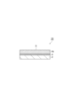
- FIG. 1 is a schematic cross-sectional view showing one embodiment of a temporary fixing laminate.
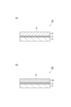
- 2(a) and 2(b) are schematic cross-sectional views showing one embodiment of a method for producing a temporary fixing laminate.
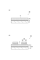
- 3A and 3B are schematic cross-sectional views showing an embodiment of a method for manufacturing a semiconductor device.
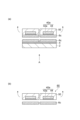
- 4A, 4B, and 4C are schematic cross-sectional views showing an embodiment of a method for manufacturing a semiconductor device.
- 5A and 5B are schematic cross-sectional views showing an embodiment of a method for manufacturing a semiconductor device.
- a numerical range indicated using " ⁇ " indicates a range that includes the numerical values before and after " ⁇ " as the minimum and maximum values, respectively.
- the upper or lower limit value described in one numerical range may be replaced with the upper or lower limit value of another numerical range described in stages.
- the upper or lower limit value of that numerical range may be replaced with the value shown in the examples (manufacturing examples).
- the term “layer” includes structures that are formed over the entire surface when viewed in a plan view, as well as structures that are formed on only a portion of the surface.
- the term “process” includes not only independent processes, but also processes that cannot be clearly distinguished from other processes as long as the intended effect of the process is achieved.
- (meth)acrylate means acrylate or the corresponding methacrylate.
- the materials exemplified below may be used alone or in combination of two or more types within the range that meets the conditions.
- the content of each component means the total amount of those multiple substances unless otherwise specified.
- the temporary fixing laminate of this embodiment is used to temporarily fix a semiconductor member and a support member.
- Fig. 1 is a schematic cross-sectional view showing one embodiment of the temporary fixing laminate.
- the temporary fixing laminate 20 shown in Fig. 1 has a support member 2, a light absorbing layer 4, and a temporary fixing material layer 6c containing a cured product of a thermosetting resin component, in this order from the support member 2.
- the temporary fixing material layer 6c has a surface S on the side of the temporary fixing material layer 6c on which the semiconductor member is arranged (the side opposite to the light absorbing layer 4).
- the support member 2 is a plate-like body that has high transmittance and can withstand the load applied during processing of the semiconductor member.
- Examples of the support member 2 include an inorganic glass substrate and a transparent resin substrate.
- the thickness of the support member 2 may be, for example, 0.1 to 2.0 mm. If the thickness of the support member 2 is 0.1 mm or more, handling tends to be easier. If the thickness of the support member 2 is 2.0 mm or less, material costs tend to be reduced.
- the light absorbing layer 4 is a layer that absorbs light and generates heat.
- the light absorbing layer 4 may be, for example, a conductor layer containing a conductor that absorbs light and generates heat.
- conductors that constitute the conductor layer include metals, metal oxides, and conductive carbon materials.
- the metals may be simple metals such as chromium, copper, titanium, silver, platinum, and gold, or alloys such as nickel-chromium, stainless steel, and copper-zinc.
- metal oxides include indium tin oxide (ITO), zinc oxide, and niobium oxide.
- the conductors may be chromium, titanium, or conductive carbon materials.
- the light absorbing layer 4 may be, for example, a conductor-containing resin layer that contains a conductor that absorbs light and generates heat, and a resin.
- the light absorbing layer 4 may be a metal layer consisting of a single layer or multiple layers, for example, a metal layer consisting of a copper layer and a titanium layer.
- the light absorbing layer 4 may contain at least one metal selected from the group consisting of tantalum (Ta), platinum (Pt), nickel (Ni), titanium (Ti), tungsten (W), chromium (Cr), copper (Cu), aluminum (Al), silver (Ag), and gold (Au).
- the light absorbing layer 4 may be composed of two layers, a first layer and a second layer, and may be laminated in this order from the support member 2 side.
- the first layer of the light absorbing layer 4 may contain at least one metal selected from the group consisting of tantalum (Ta), platinum (Pt), nickel (Ni), titanium (Ti), tungsten (W), and chromium (Cr)
- the second layer of the light absorbing layer 4 may contain at least one metal selected from the group consisting of copper (Cu), aluminum (Al), silver (Ag), and gold (Au).
- the thickness of the light absorbing layer 4 may be 1 to 5000 nm, 100 to 3000 nm, or 50 to 300 nm from the viewpoint of easy peelability.
- the thickness of the light absorbing layer 4 (or metal layer) may be 75 nm or more, 90 nm or more, or 100 nm or more from the viewpoint of good peelability, and may be 1000 nm or less, 800 nm or less, 500 nm or less, or 300 nm or less.
- the thickness of the light absorbing layer 4 may be 100 nm or more, 125 nm or more, 150 nm or more, or 200 nm or more, and may be 1000 nm or less, 800 nm or less, or 500 nm or less from the viewpoint of good peelability.
- the thickness of the light absorbing layer 4 may be 1 to 50 ⁇ m, may be 1 ⁇ m or more, 5 ⁇ m or more, or 10 ⁇ m or more, and may be 50 ⁇ m or less, 30 ⁇ m or less, or 20 ⁇ m or less.
- the surface S of the temporary fixing layer 6c is subjected to a nanoindentation method using a Berkovich indenter at 25°C, with the load increased at a loading rate of 20 ⁇ N/sec for 5 seconds, and after the load reaches 100 ⁇ N, the load is held at 100 ⁇ N for 2 seconds, and the load is reduced at an unloading rate of 20 ⁇ N/sec for 5 seconds until the load is unloaded to 0 mN.
- the indentation depth is 600 nm or more, the semiconductor member and the support member can be sufficiently fixed via the light absorbing layer and the temporary fixing layer, even after the thermosetting resin component is thermally cured.
- the indentation depth may be 650 nm or more, 700 nm or more, 750 nm or more, 800 nm or more, 850 nm or more, or 900 nm or more.
- the indentation depth may be, for example, 2000 nm or less, 1500 nm or less, or 1200 nm or less.
- the indentation depth can be measured by performing an indentation test using a nanoindenter and a Berkovich indenter in accordance with ISO 14577. More specifically, a thermosetting resin layer (thermosetting resin film) containing a thermosetting resin component with a thickness of 50 ⁇ m is first prepared on a support film (the preparation of the thermosetting resin film will be described later). Next, the thermosetting resin layer (thermosetting resin film) is attached to a slide glass using a roll laminator, the support film is peeled off, and a laminate containing a slide glass and a thermosetting resin layer provided on the slide glass is obtained.
- the surface of the thermosetting resin layer in contact with the support film is the surface S (the surface on the side where the semiconductor member is arranged) of the temporary fixing material layer 6c.
- the laminate may be a temporary fixing laminate described later.
- the prepared laminate is heated in a dryer at 200°C for 1 hour to cure the thermosetting resin component of the thermosetting resin layer, and a temporary fixing material layer containing a cured product of the thermosetting resin component is formed to obtain a test specimen.
- the obtained test specimen is fixed to the stage of a nanoindenter, and a Berkovich indenter is brought into contact with the surface of the temporary fixing material layer of the test specimen, and an indentation test is performed in which the load is increased for 5 seconds at a loading rate of 20 ⁇ N/s under the condition of 25°C, and after the load reaches 100 ⁇ N, it is held at 100 ⁇ N for 2 seconds, and the load is reduced for 5 seconds at an unloading rate of 20 ⁇ N/s to 0 mN, and the depth to which the Berkovich indenter is pressed into the temporary fixing material layer is measured using a nanoindenter.
- the indentation test is performed at any 5 points, and the median of the obtained depths is taken as the indentation depth.
- Indenter Berkovich indenter Loading speed: 20 ⁇ N/sec Loading time: 5 seconds (Maximum load: 100 ⁇ N) Holding time: 2 seconds Unloading speed: 20 ⁇ N/second
- the surface roughness (arithmetic mean roughness Ra (JIS B 0601-2001)) of the surface S may be 50 nm or less. If the surface roughness is 50 nm or less, the semiconductor member and the support member tend to be more sufficiently fixed via the light absorbing layer and the temporary fixing material layer, even after the thermosetting resin component is thermally cured.
- the surface roughness may be 40 nm or less, 30 nm or less, 25 nm or less, 20 nm or less, 15 nm or less, 10 nm or less, 8 nm or less, or 5 nm or less.
- the surface roughness may be, for example, 0.1 nm or more or 1 nm or more.
- the surface roughness can be determined by preparing a test specimen similar to that used in the indentation test, and measuring the surface of the temporary fixing material layer of the test specimen using a stylus-type step surface shape measuring device. There are no particular limitations on the measurement conditions, but examples include the conditions shown below.
- the surface tack strength at 30°C on the surface S may be 9.8 x 10⁻³ N (1.0 gf) or more. If the surface tack strength is 9.8 x 10⁻³ N (1.0 gf) or more, even after the thermosetting resin component is thermally cured, the semiconductor member and the support member tend to be more sufficiently fixed via the light absorbing layer and the temporary fixing material layer.
- the surface tack strength may be 2.0 x 10⁻² N (2.0 gf) or more, 2.9 x 10⁻² N (3.0 gf) or more, 3.4 x 10⁻² N (3.5 gf) or more, 3.9 x 10⁻² N (4.0 gf) or more, 4.4 x 10⁻² N (4.5 gf) or more, or 4.9 x 10⁻² N (5.0 gf) or more.
- the surface tack strength may be, for example, 2.0 ⁇ 10 ⁇ 1 N (20 gf) or less, 1.5 ⁇ 10 ⁇ 1 N (15 gf) or less, or 9.8 ⁇ 10 ⁇ 2 N (10 gf) or less.
- Probe Made of SUS (stainless steel), diameter 5 mm Push-in/peel-off speed: 600 mm/sec Push-in time: 1 sec
- the temporary fixing material layer 6c contains a cured product of a thermosetting resin component, and the thermosetting resin layer or the thermosetting resin film for forming the same contains a thermosetting resin component.
- the thermosetting resin component can be selected from any one that satisfies the prescribed conditions for the indentation depth of the temporary fixing material layer containing the cured product of the thermosetting resin component.
- the thermosetting resin component may contain, for example, a thermoplastic resin and a thermosetting resin, since the indentation depth, surface roughness, surface tackiness, etc. tend to easily satisfy the prescribed conditions.
- the thermoplastic resin may contain a hydrocarbon resin.
- Thermoplastic resin is a resin that has thermoplastic properties, or at least has thermoplastic properties in an uncured state and forms a crosslinked structure after heating.
- thermoplastic resins include hydrocarbon resins, polycarbonates, polyphenylene sulfides, polyethersulfones, polyetherimides, polyimides, petroleum resins, and novolac resins.
- the thermoplastic resin may contain a hydrocarbon resin or may be a hydrocarbon resin.
- Hydrocarbon resins are resins whose main skeleton is composed of hydrocarbons.
- hydrocarbon resins include ethylene-propylene copolymers, ethylene-1-butene copolymers, ethylene-propylene-1-butene copolymer elastomers, ethylene-1-hexene copolymers, ethylene-1-octene copolymers, ethylene-styrene copolymers, ethylene-norbornene copolymers, propylene-1-butene copolymers, ethylene-propylene-non-conjugated diene copolymers, ethylene-1-butene-non-conjugated diene copolymers, ethylene-propylene-1-butene-non-conjugated diene copolymers, polyisoprene, polybutadiene, styrene-butadiene-styrene block copolymers (SBS), styrene-
- hydrocarbon resins may be hydrogenated. These hydrocarbon resins may also be carboxy-modified with maleic anhydride or the like.
- the hydrocarbon resin may contain a hydrocarbon resin having a monomer unit derived from styrene (i.e., a styrene-based resin), or may be a styrene-based resin. More specifically, the hydrocarbon resin may contain a styrene-ethylene-butylene-styrene block copolymer (SEBS), or may be a styrene-ethylene-butylene-styrene block copolymer (SEBS).
- SEBS styrene-ethylene-butylene-styrene block copolymer
- SEBS styrene-ethylene-butylene-styrene block copolymer
- the content of the hydrocarbon resin (or styrene-based resin) may be 50% by mass or more, 70% by mass or more, or 90% by mass or more based on the total amount of the thermoplastic resin.
- the content of the hydrocarbon resin (or styrene-based resin) may be 100% by mass or less based on the total amount of the thermoplastic resin.
- the thermoplastic resin may be composed of a hydrocarbon resin (or a styrene-based resin).
- the content of the styrene-based resin (or SEBS) may be 50 mass% or more, 70 mass% or more, or 90 mass% or more based on the total amount of the hydrocarbon resin.
- the content of the styrene-based resin (or SEBS) may be 100 mass% or less based on the total amount of the hydrocarbon resin.
- the hydrocarbon resin may be composed of a styrene-based resin (or SEBS).
- the content of the monomer units derived from styrene may be 10 to 22.5% by mass based on the total amount of the hydrocarbon resin (or thermoplastic resin).
- the content of the monomer units derived from styrene is in this range, the storage modulus of the thermosetting resin film tends to be easily adjusted to a desired range, and the effects of the present disclosure tend to be significantly achieved.
- the content of the monomer units derived from styrene means the total content of the monomer units derived from styrene in the two or more types of styrene-based resins.
- the content of the monomer units derived from styrene may be 11% by mass or more, 12% by mass or more, or 13% by mass or more, based on the total amount of the hydrocarbon resin (or thermoplastic resin), and may be 22% by mass or less, or 21.5% by mass or less.
- thermosetting resin component contains a styrene-based resin as a thermoplastic resin (hydrocarbon resin)
- the content of the monomer units derived from styrene may be 7 to 16 mass% based on the total amount of the thermosetting resin component.
- the storage modulus of the thermosetting resin film tends to be easily adjusted to a desired range, and the effects of the present disclosure tend to be significantly achieved.
- the content of the monomer units derived from styrene means the total content of the monomer units derived from styrene in the two or more types of styrene-based resins.
- the content of the monomer units derived from styrene may be 7.5 mass% or more, 8 mass% or more, or 9 mass% or more, based on the total amount of the thermosetting resin component, and may be 15.5 mass% or less, or 15 mass% or less.
- the Tg of the thermoplastic resin may be -100 to 500°C, -50 to 300°C, or -50 to 50°C. If the Tg of the thermoplastic resin is 500°C or less, flexibility is easily ensured when a film-like temporary fixing material is formed, and low-temperature application properties tend to be improved. If the Tg of the thermoplastic resin is -100°C or more, deterioration in handleability and peelability caused by excessive flexibility when a film-like temporary fixing material is formed tends to be suppressed.
- the Tg of a thermoplastic resin is the midpoint glass transition temperature obtained by differential scanning calorimetry (DSC). Specifically, the Tg of a thermoplastic resin is the midpoint glass transition temperature calculated by a method in accordance with JIS K7121:2012, measuring the change in heat quantity under conditions of a heating rate of 10°C/min and a measurement temperature of -80 to 80°C.
- the weight average molecular weight (Mw) of the thermoplastic resin may be 10,000 to 5,000,000 or 100,000 to 2,000,000. If the weight average molecular weight is 10,000 or more, it tends to be easier to ensure the heat resistance of the temporary fixing material layer that is formed. If the weight average molecular weight is 5,000,000 or less, it tends to be easier to suppress a decrease in flow and adhesion when a thermosetting resin film is formed.
- the weight average molecular weight is a polystyrene-equivalent value obtained by using a calibration curve with standard polystyrene in gel permeation chromatography (GPC).
- the content of the thermoplastic resin may be, for example, 40 to 90 mass% based on the total amount of the thermosetting resin components.
- the content of the thermoplastic resin may be, for example, 50 mass% or more or 60 mass% or more based on the total amount of the thermosetting resin components, and may be 85 mass% or less or 80 mass% or less.
- the content of the thermoplastic resin is in such a range, the thin film formability and flatness of the temporary fixing material layer tend to be superior.
- Thermosetting resin is a resin that exhibits hardening properties due to heat, and is a concept that does not include the above-mentioned thermoplastic resins (hydrocarbon resins).
- thermosetting resins include epoxy resins, acrylic resins, silicone resins, phenolic resins, thermosetting polyimide resins, polyurethane resins, melamine resins, and urea resins.
- the thermosetting resin may be epoxy resin, as it has superior heat resistance, workability, and reliability.
- the epoxy resin is not particularly limited as long as it hardens and has heat resistance.
- epoxy resins include bifunctional epoxy resins such as bisphenol A type epoxy, novolac type epoxy resins such as phenol novolac type epoxy resins and cresol novolac type epoxy resins, and alicyclic epoxy resins such as dicyclopentadiene type epoxy resins.
- the epoxy resin may also be, for example, a multifunctional epoxy resin, a glycidylamine type epoxy resin, or a heterocycle-containing epoxy resin.
- the epoxy resin may contain an alicyclic epoxy resin from the viewpoint of heat resistance and weather resistance.
- the thermosetting resin may be a combination of an epoxy resin and an epoxy resin curing agent.
- the epoxy resin curing agent may be a commonly used known curing agent.
- Examples of epoxy resin curing agents include amines, polyamides, acid anhydrides, polysulfides, boron trifluoride, bisphenols (bisphenol A, bisphenol F, bisphenol S, etc.), phenolic resins (phenol novolac resin, bisphenol A type novolac resin, cresol novolac resin, phenol aralkyl resin, etc.), etc.
- the content of the thermosetting resin may be, for example, 10 to 60 mass% based on the total amount of the thermosetting resin components.
- the content of the thermosetting resin may be, for example, 15 mass% or more or 20 mass% or more based on the total amount of the thermosetting resin components, and may be 50 mass% or less or 40 mass% or less.
- the content of the thermosetting resin is in such a range, the thin film formability and flatness of the temporary fixing material layer tend to be superior.
- the thermosetting resin component may further contain a curing accelerator that accelerates the curing reaction of a thermosetting resin such as an epoxy resin.
- a curing accelerator such as imidazole derivatives, dicyandiamide derivatives, dicarboxylic acid dihydrazide, triphenylphosphine, tetraphenylphosphonium tetraphenylborate, 2-ethyl-4-methylimidazole-tetraphenylborate, and 1,8-diazabicyclo[5,4,0]undecene-7-tetraphenylborate.
- the content of the curing accelerator may be 0.01 to 5 mass% based on the total amount of the thermosetting resin. When the content of the curing accelerator is within this range, the curing of the thermosetting resin component and the heat resistance after curing tend to be better.
- the content of the curing accelerator may be 1.0 mass% or more, 1.2 mass% or more, or 1.5 mass% or more based on the total amount of the thermosetting resin, since it is easy to adjust the storage modulus at 270°C and the storage modulus at 25°C to a predetermined range, and may be 3.0 mass% or less, 2.5 mass% or less, or 2.0 mass% or less.
- the thermosetting resin component may further include a polymerizable monomer and a polymerization initiator.
- the polymerizable monomer is not particularly limited as long as it is polymerized by heating or irradiation with ultraviolet light or the like. From the viewpoint of material selectivity and ease of availability, the polymerizable monomer may be, for example, a compound having a polymerizable functional group such as an ethylenically unsaturated group. Examples of the polymerizable monomer include (meth)acrylate, vinylidene halide, vinyl ether, vinyl ester, vinyl pyridine, vinyl amide, and arylated vinyl. Of these, the polymerizable monomer may be a (meth)acrylate. The (meth)acrylate may be monofunctional (monofunctional), bifunctional, or trifunctional or higher, but from the viewpoint of obtaining sufficient curability, it may be a bifunctional or higher (meth)acrylate.
- the content of the polymerizable monomer may be 0 to 50 mass % based on the total amount of the thermosetting resin components.
- the polymerization initiator is not particularly limited as long as it initiates polymerization by heating or irradiation with ultraviolet light or the like.
- the polymerization initiator may be a thermal radical polymerization initiator or a photoradical polymerization initiator.
- the content of the polymerization initiator may be 0.01 to 5 mass% based on the total amount of polymerizable monomers.
- thermosetting resin component may be the main component of the thermosetting resin layer (thermosetting resin film).
- the content of the thermosetting resin component may be 70% by mass or more, 80% by mass or more, 90% by mass or more, 95% by mass or more, or 98% by mass or more based on the total amount of the thermosetting resin layer (thermosetting resin film).
- thermosetting resin layer may contain other components in addition to the thermosetting resin component.
- other components include insulating fillers, sensitizers, antioxidants, etc.
- the insulating filler may be added for the purpose of imparting low thermal expansion, low moisture absorption, etc. to the temporary fixing material layer.
- the insulating filler include non-metallic inorganic fillers such as silica, alumina, boron nitride, titania, glass, and ceramic.
- the insulating filler may be particles whose surfaces have been treated with a surface treatment agent.
- the surface treatment agent may be, for example, a silane coupling agent.
- the content of the insulating filler may be 0.1 to 20 mass % based on the total amount of the thermosetting resin components. When the content of the insulating filler is within this range, there is a tendency to be able to further improve heat resistance without impeding light transmission. In addition, when the content of the insulating filler is within this range, it may also contribute to easy peelability.
- Sensitizers include, for example, anthracene, phenanthrene, chrysene, benzopyrene, fluoranthene, rubrene, pyrene, xanthone, indanthrene, thioxanthene-9-one, 2-isopropyl-9H-thioxanthene-9-one, 4-isopropyl-9H-thioxanthene-9-one, 1-chloro-4-propoxythioxanthone, etc.
- the content of the sensitizer may be 0.01 to 10 mass% based on the total amount of the thermosetting resin component. If the content of the sensitizer is within this range, it tends to have less effect on the properties and thin film properties of the thermosetting resin component.
- antioxidants examples include quinone derivatives such as benzoquinone and hydroquinone, phenol derivatives (hindered phenol derivatives) such as 4-methoxyphenol and 4-t-butylcatechol, aminoxyl derivatives such as 2,2,6,6-tetramethylpiperidine-1-oxyl and 4-hydroxy-2,2,6,6-tetramethylpiperidine-1-oxyl, and hindered amine derivatives such as tetramethylpiperidyl methacrylate.
- quinone derivatives such as benzoquinone and hydroquinone
- phenol derivatives hindered amine derivatives
- hindered amine derivatives such as tetramethylpiperidyl methacrylate.
- the content of the antioxidant may be 0.1 to 10 mass% based on the total amount of the thermosetting resin components. If the content of the antioxidant is within this range, it tends to suppress the decomposition of the thermosetting resin components and prevent contamination.
- the temporary fixing laminate 20 can be obtained, for example, by a method including a step of preparing a laminate precursor 10 having a support member 2, a light absorbing layer 4, and a thermosetting resin layer 6 containing a thermosetting resin component, in that order, from the support member 2, and a step of heating the laminate precursor 10 to form a temporary fixing material layer 6c containing a cured product of the thermosetting resin component.
- the laminate precursor 10 can be obtained, for example, by a method including a step of providing a light absorbing layer 4 on a support member 2, and a step of attaching a thermosetting resin film containing a thermosetting resin component onto the light absorbing layer 4 to form a thermosetting resin layer 6.
- the light absorbing layer 4 can be provided on the support member 2 by performing physical vapor deposition (PVD) such as vacuum deposition or sputtering, or chemical vapor deposition (CVD) such as plasma-enhanced chemical vapor deposition.
- PVD physical vapor deposition
- CVD chemical vapor deposition
- the light absorbing layer 4 can also be provided on the support member 2 by performing electrolytic plating or electroless plating. With physical vapor deposition, the light absorbing layer 4 that covers the surface of the support member 2 can be efficiently formed even if the support member 2 has a large area.
- thermosetting resin film for forming the thermosetting resin layer 6 is prepared, for example, by first dissolving or dispersing the components constituting the thermosetting resin component described above in a solvent by stirring, mixing, kneading, etc., to prepare a varnish of the thermosetting resin component.
- the varnish of the thermosetting resin component is then applied to a support film that has been subjected to a release treatment using a knife coater, roll coater, applicator, comma coater, die coater, etc., and the solvent is then volatilized by heating to form a thermosetting resin film made of the thermosetting resin component on the support film.
- the thickness of the thermosetting resin film can be adjusted by adjusting the amount of varnish of the thermosetting resin component applied.
- the solvent used in preparing the varnish of the thermosetting resin component is not particularly limited as long as it has the property of being able to uniformly dissolve or disperse each component.
- solvents include aromatic hydrocarbons such as toluene, xylene, mesitylene, cumene, and p-cymene; aliphatic hydrocarbons such as hexane and heptane; cyclic alkanes such as methylcyclohexane; cyclic ethers such as tetrahydrofuran and 1,4-dioxane; ketones such as acetone, methyl ethyl ketone, methyl isobutyl ketone, cyclohexanone, and 4-hydroxy-4-methyl-2-pentanone; esters such as methyl acetate, ethyl acetate, butyl acetate, methyl lactate, ethyl lactate, and ⁇ -butyrolactone; carbonates such as ethylene carbonate
- the solvent may be toluene, xylene, heptane, or cyclohexanone from the standpoint of solubility and boiling point.
- the solid component concentration in the varnish may be 10 to 80% by mass based on the total mass of the varnish.
- the stirring, mixing or kneading of the thermosetting resin component when preparing the varnish can be carried out using, for example, a stirrer, a mixing machine, a triple roll mill, a ball mill, a bead mill, a homodisper, etc.
- the support film examples include polyesters such as polyethylene terephthalate (PET), polybutylene terephthalate, and polyethylene naphthalate; polyolefins such as polyethylene and polypropylene; polycarbonate, polyamide, polyimide, polyamideimide, polyetherimide, polyethersulfide, polyethersulfone, polyetherketone, polyphenylene ether, polyphenylene sulfide, poly(meth)acrylate, polysulfone, and liquid crystal polymer films.
- the thickness of the support film may be, for example, 1 to 250 ⁇ m.
- the heating conditions for volatilizing the solvent from the varnish of the thermosetting resin component applied to the support film can be set appropriately according to the solvent used, etc. Heating conditions may be, for example, 40 to 120°C for 0.1 to 30 minutes.
- Methods for attaching a thermosetting resin film onto the light absorbing layer 4 include, for example, roll lamination, vacuum lamination, and heat pressing. Lamination can be performed under temperature conditions of, for example, 0 to 120°C.
- the thickness of the thermosetting resin layer 6 may be, for example, 0.1 ⁇ m or more, 1 ⁇ m or more, or 5 ⁇ m or more, and may be 200 ⁇ m or less, 100 ⁇ m or less, or 70 ⁇ m or less.
- thermosetting resin component of the thermosetting resin layer 6 of the obtained laminate precursor 10 is thermally cured to form a temporary fixing material layer 6c containing a cured product of the thermosetting resin component.
- the thermal curing conditions may be, for example, 150 to 300°C or less or 180 to 250°C, and 1 to 180 minutes or 10 to 120 minutes.
- the thickness of the temporary fixing material layer 6c may be, for example, 0.1 ⁇ m or more, 1 ⁇ m or more, or 5 ⁇ m or more, and may be 200 ⁇ m or less, 100 ⁇ m or less, or 70 ⁇ m or less.
- the method for manufacturing a semiconductor device of this embodiment includes a step of preparing the temporary fixing laminate (preparation step), a step of temporarily fixing a semiconductor member to a support member via a light absorbing layer and a temporary fixing material layer (temporary fixing step), a step of processing the semiconductor member temporarily fixed to the support member (processing step), and a step of irradiating the light absorbing layer of the temporary fixing laminate from the support member side with light to separate the semiconductor member from the support member (separation step).
- the temporary fixing laminate since the temporary fixing laminate is used, the semiconductor member and the support member can be sufficiently fixed, and further, it becomes possible to easily separate the processed semiconductor member from the support member while suppressing the generation of residue.
- (Preparation process) 3(a) and 3(b) are schematic cross-sectional views showing one embodiment of a method for manufacturing a semiconductor device.
- the above-mentioned temporary fixing laminate 20 for temporarily fixing a semiconductor member to a support member during processing of the semiconductor member is prepared in order to manufacture a semiconductor device (see FIG. 3(a)).
- the semiconductor member 40 is temporarily fixed to the support member 2 via the light absorbing layer 4 and the temporary fixing material layer 6c.
- the temporary fixing material layer 6c has a surface S on the opposite side of the temporary fixing material layer 6c from the light absorbing layer 4.
- the semiconductor member 40 can be temporarily fixed to the support member 2 by pressing the semiconductor member 40 in a state in which the semiconductor member 40 is arranged on the temporary fixing material layer 6c (see FIG. 3B) (see FIG. 3B).
- the semiconductor member 40 can be temporarily bonded to the support member 2 via the light absorbing layer 4 and the temporary fixing material layer 6c containing a cured product of a thermosetting resin component. In this way, a laminate 30 including the temporary fixing laminate 20 and the semiconductor member 40 provided on the temporary fixing material layer 6c of the temporary fixing laminate 20 is formed.
- the semiconductor member 40 may, for example, have a semiconductor substrate 42 and a rewiring layer 44.
- the semiconductor member 40 is temporarily fixed to the support member 2 via the light absorbing layer 4 and the temporary fixing material layer 6c with the rewiring layer 44 facing the temporary fixing material layer 6c.
- the semiconductor member 40 may further have an external connection terminal.
- the semiconductor substrate 42 may be a semiconductor wafer or a semiconductor chip obtained by dividing a semiconductor wafer. In the example of FIG. 3(a), multiple semiconductor members 40 are arranged on the surface S of the temporary fixing material layer 6c, but the number of semiconductor members 40 may be one.
- the thickness of the semiconductor member 40 may be 1 to 1000 ⁇ m, 10 to 500 ⁇ m, or 20 to 200 ⁇ m from the viewpoint of miniaturization and thinning of the semiconductor device as well as suppression of cracks during transportation and processing.
- the semiconductor member 40 arranged on the temporary fixing material layer 6c is pressed against the temporary fixing material layer 6c using, for example, a vacuum press or a vacuum laminator.
- the pressing conditions may be an atmospheric pressure of 1 hPa or less, a pressing pressure of 1 MPa, a pressing temperature of 120 to 200°C, and a holding time of 100 to 300 seconds.
- the pressing conditions may be, for example, an atmospheric pressure of 1 hPa or less, a pressing temperature of 60 to 180°C or 80 to 150°C, a laminating pressure of 0.01 to 1.0 MPa or 0.1 to 0.7 MPa, and a holding time of 1 to 600 seconds or 30 to 300 seconds.
- FIG. 4(a) shows an example of processing including thinning of a semiconductor substrate, and a semiconductor member 40a after processing has a thinned semiconductor substrate 42a and a rewiring layer 44.
- the processing of the semiconductor member is not limited to this, and can include, for example, thinning of a semiconductor substrate, division (dicing) of a semiconductor member, formation of a through electrode (silicon through electrode), etching, plating reflow processing, sputtering, or a combination thereof.
- a sealing layer 50 is formed to seal the processed semiconductor member 40a, as shown in FIG. 4(b).
- the sealing layer 50 can be formed using a sealing material that is typically used for manufacturing semiconductor elements.
- the sealing layer 50 may be formed from a thermosetting resin composition.
- the thermosetting resin composition used in the sealing layer 50 include epoxy resins such as cresol novolac epoxy resin, phenol novolac epoxy resin, biphenyl diepoxy resin, and naphthol novolac epoxy resin.
- the sealing layer 50 and the thermosetting resin composition for forming the sealing layer 50 may contain additives such as a filler and/or a flame retardant.
- the sealing layer 50 is formed using, for example, a solid material, a liquid material, a fine-grained material, or a sealing film.
- a sealing film When a sealing film is used, a compression sealing molding machine, a vacuum laminating device, or the like is used.
- the sealing layer 50 can be formed by covering the processed semiconductor member 40a with a sealing film that has been thermally melted under conditions of 40 to 180°C (or 60 to 150°C), 0.1 to 10 MPa (or 0.5 to 8 MPa), and 0.5 to 10 minutes.
- the thickness of the sealing film is adjusted so that the sealing layer 50 is equal to or greater than the thickness of the processed semiconductor member 40a.
- the thickness of the sealing film may be 50 to 2000 ⁇ m, 70 to 1500 ⁇ m, or 100 to 1000 ⁇ m.
- the sealing layer 50 and the temporary fixing material layer 6c may be divided into a plurality of parts, each of which includes one processed semiconductor member 40a.
- (Separation process) 5(a) and 5(b) are schematic cross-sectional views showing an embodiment of a method for manufacturing a semiconductor device.
- the separation step the light absorbing layer of the temporary fixing laminate is irradiated with light from the support member side to separate the semiconductor member from the support member.
- the light absorbing layer 4 of the temporary fixing laminate 20 is irradiated with light A from the support member 2 side to separate the processed semiconductor member 40a from the support member 2.
- the light absorbing layer 4 absorbs the light and generates heat instantaneously.
- the generated heat may cause, for example, melting of the temporary fixing material layer 6c, thermal stress between the support member 2 and the processed semiconductor member 40a, and scattering of the light absorbing layer 4.
- One or more of these phenomena may be the main cause of cohesive peeling, interfacial peeling, etc., and the processed semiconductor member 40a may be easily separated from the support member 2.
- a slight stress may be applied to the processed semiconductor member 40a along with the irradiation with light A.
- Light A includes at least infrared light.
- the wavelength of infrared light is usually 700 nm to 1 mm.
- the light A in the separation process may be coherent light.
- Coherent light is an electromagnetic wave with properties such as high coherence, high directionality, and high monochromaticity. Coherent light tends to be high in intensity because light of the same wavelength and phase is reinforced and synthesized.
- Laser light is generally coherent light. Examples of laser light include YAG laser, fiber laser, semiconductor laser, helium-neon laser, argon laser, and excimer laser.
- the wavelength of the laser light may be 1300 nm or less. By having a wavelength of 1300 nm or less, the light absorption of the support member 2 is suppressed and the light absorption of the metal layer 12 is increased, making it possible to peel off with lower light irradiation energy.
- the coherent light may be pulsed light.
- the light A in the separation process may be incoherent light.
- Incoherent light is not coherent light, and is an electromagnetic wave with properties such as no interference fringes, low coherence, and low directivity. Incoherent light tends to attenuate as the optical path length increases. Light such as sunlight and fluorescent light is incoherent light. Incoherent light can also be said to be light other than laser light.
- the irradiation area of incoherent light is generally primarily larger than that of coherent light (i.e., laser light), so it is possible to reduce the number of irradiations. For example, a single irradiation can cause separation of multiple processed semiconductor members 40a.
- the incoherent light may include infrared light.
- the incoherent light may be pulsed light.
- the light source is not particularly limited, but may be a xenon lamp.
- a xenon lamp is a lamp that uses light emission caused by application and discharge in an arc tube filled with xenon gas.
- Xenon lamps discharge while repeatedly ionizing and exciting, so they have a stable continuous wavelength range from the ultraviolet to infrared regions. Xenon lamps require less time to start up than lamps such as metal halide lamps, so the time required for the process can be significantly reduced. Furthermore, since a high voltage must be applied to emit light, high heat is generated instantaneously, but xenon lamps are also advantageous in that they require less time to cool down and allow for continuous work.
- the irradiation conditions of the xenon lamp include the applied voltage, pulse width, irradiation time, irradiation distance (the distance between the light source and the temporary fixing material layer), irradiation energy, etc., and these can be set arbitrarily according to the number of irradiations, etc. From the viewpoint of reducing damage to the processed semiconductor member 40a, the irradiation conditions may be set so that the processed semiconductor member 40a can be separated with a single irradiation.
- a part of the temporary fixing material layer 6c may remain on the separated semiconductor member 40a after processing as residue.
- the remaining residue is removed as shown in FIG. 5(b).
- the remaining residue may be removed, for example, by washing with a solvent or by peeling.
- the solvent include, but are not limited to, ethanol, methanol, toluene, xylene, acetone, methyl ethyl ketone, methyl isobutyl ketone, and hexane. These may be used alone or in combination of two or more.
- the processed semiconductor member 40a may be immersed in a solvent or ultrasonically cleaned.
- the processed semiconductor member 40a may be heated at a low temperature of about 100° C. or less.
- the above-described exemplary method can provide a semiconductor element 60 including a processed semiconductor member 40a.
- the obtained semiconductor element 60 can be connected to another semiconductor chip or a semiconductor element mounting substrate to manufacture a semiconductor device.
- thermosetting resin film Preparation of Thermosetting Resin Film and Evaluation of Temporary Fixing Material Layer ⁇ Preparation of Thermosetting Resin Film> The following components were used in preparing the thermosetting resin film:
- A Thermoplastic resin
- A-1a Maleic anhydride-modified styrene-ethylene-butylene-styrene block copolymer (Tuftec M1913, manufactured by Asahi Kasei Corporation, styrene content: 30% by mass), used as a 25% by mass xylene solution
- A-2a Maleic anhydride-modified styrene-ethylene-butylene-styrene block copolymer (Tuftec M1943, manufactured by Asahi Kasei Corporation, styrene content: 20% by mass), used as a 25% by mass xylene solution
- a-1b Phenoxy resin (Phenototo ZX-1356-2, manufactured by Nippon Steel Chemical & Material Co., Ltd.), used as a 25% by mass cyclohexanone solution
- B Thermosetting resin
- B-1a Dicyclopentadiene-type ethylene-butylene-styren
- thermosetting resin component The materials shown in Table 1 were mixed in the ratios shown in Table 1 (unit: parts by mass, the values in Table 1 indicate the non-volatile content) to obtain a varnish of a thermosetting resin component.
- the obtained varnish of a thermosetting resin component was applied to the release-treated surface of a polyethylene terephthalate (PET) film (Purex A31, manufactured by Toyobo Film Solutions Co., Ltd., thickness: 38 ⁇ m) as a support film using a precision coater.
- PET polyethylene terephthalate
- the coating was dried by heating at 100°C for 10 minutes to obtain the thermosetting resin films of Production Examples 1 to 5 with a thickness of 50 ⁇ m.
- Indentation depth was measured by performing an indentation test using a nanoindenter (Hysitron TI980, Bruker Japan Co., Ltd.) using a Berkovich indenter in accordance with ISO14577.
- Each thermosetting resin film was attached to a slide glass using a roll laminator, the support film was peeled off, and a laminate including a slide glass and a thermosetting resin layer provided on the slide glass was obtained.
- the surface of the thermosetting resin layer in contact with the support film is the surface of the temporary fixing material layer on which the semiconductor member is arranged.
- the prepared laminate was heated in a dryer under conditions of 200 ° C. and 1 hour to harden the thermosetting resin component of the thermosetting resin layer, and a temporary fixing material layer including a cured product of the thermosetting resin component was formed, thereby obtaining test specimens having the temporary fixing material layers of Production Examples 1 to 5.
- the obtained test specimen was fixed on the stage of a nanoindenter, and a Berkovich indenter was brought into contact with the surface of the temporary fixing material layer of the test specimen.
- the load was increased for 5 seconds at a loading rate of 20 ⁇ N/sec. After the load reached 100 ⁇ N, it was held at 100 ⁇ N for 2 seconds, and then reduced to 0 mN at an unloading rate of 20 ⁇ N/sec for 5 seconds.
- An indentation test was then performed, and the depth to which the Berkovich indenter was pressed into the temporary fixing material layer was measured using a nanoindenter. The indentation test was performed at any 5 points, and the median of the obtained depths was taken as the indentation depth. The results are shown in Table 1.
- the surface roughness was determined by preparing a test specimen similar to that in "1. Indentation Depth" and measuring the surface of the temporary fixing material layer of Production Examples 1 to 5 using a stylus-type step surface profiler (XP-2, manufactured by Ambios Technology). The measurement was performed under the following conditions. The results are shown in Table 1.
- Probe Made of SUS (stainless steel), diameter 5 mm Push-in/peel-off speed: 600 mm/sec Push-in time: 1 sec
- thermosetting resin films of Production Examples 1 to 5 were heated in a dryer at 200°C for 1 hour to cure the thermosetting resin component of the thermosetting resin layer, and a temporary fixing material layer containing a cured product of the thermosetting resin component of Production Examples 1 to 5 was formed. Thereafter, the support film was peeled off, and the surface of the temporary fixing material layer that was in contact with the support film was pressure-bonded to a silicon wafer using a vacuum laminator under conditions of temperature 80°C/pressure 0.5 MPa/time 120 seconds. Next, the temporary fixing material layer was cut out together with the silicon wafer to a width of 1 cm to obtain a test specimen equipped with the temporary fixing material layer of Production Examples 1 to 5.
- thermosetting resin film of Production Examples 1 to 5 opposite to the support film was temporarily bonded to a 6-inch glass wafer using a vacuum laminator under conditions of temperature 80 ° C. / pressure 0.5 MPa / time 120 seconds, and heated in a dryer at 200 ° C. for 1 hour to obtain a plurality of laminates having the temporary fixing material layers of Production Examples 1 to 5.
- a silicon wafer was bonded to the temporary fixing material layer of the laminate under weak conditions (temperature 150 ° C. / pressure 0.5 MPa / time 120 seconds) or strong conditions (temperature 150 ° C. / pressure 0.7 MPa / time 120 seconds) to obtain test specimens having the temporary fixing material layers of Production Examples 1 to 5.
- a method for manufacturing a semiconductor device includes a step of processing a semiconductor member temporarily fixed to a support member, and that is capable of sufficiently fixing the semiconductor member and the support member.
- some forms of the method for manufacturing a semiconductor device tend to be able to sufficiently reduce peeling residues after the semiconductor member and the support member are separated.
- a laminate for temporary fixing that can be used in such a method for manufacturing a semiconductor device is provided.
- 2...support member 4...light absorbing layer, 6...thermosetting resin layer, 6c...temporary fixing material layer, 10...laminated precursor, 20...laminated body for temporary fixing, 30...laminated body, 40...semiconductor member, 40a...semiconductor member after processing, 42...semiconductor substrate, 42a...semiconductor substrate after thinning, 44...rewiring layer, 50...sealing layer, 60...semiconductor element.
Landscapes
- Chemical & Material Sciences (AREA)
- Organic Chemistry (AREA)
- Chemical Kinetics & Catalysis (AREA)
- Health & Medical Sciences (AREA)
- Medicinal Chemistry (AREA)
- Polymers & Plastics (AREA)
- Engineering & Computer Science (AREA)
- Mechanical Engineering (AREA)
- Laminated Bodies (AREA)
Abstract
半導体装置の製造方法が開示される。当該半導体装置の製造方法は、支持部材と、光吸収層と、熱硬化性樹脂成分の硬化物を含む仮固定材層とを支持部材からこの順序で有する仮固定用積層体を準備する工程と、半導体部材を、光吸収層及び仮固定材層を介して支持部材に対して仮固定する工程と、支持部材に対して仮固定された半導体部材を加工する工程と、仮固定用積層体の光吸収層に対して支持部材側から光を照射して、支持部材から半導体部材を分離する工程とを備える。仮固定材層の半導体部材が配置される側の表面において、バーコビッチ圧子を用いたナノインデンテーション法で、25℃の条件下、20μN/秒の負荷速度で5秒間負荷を増加させ、負荷が100μNまで達した後、100μNで2秒間保持し、20μN/秒の除荷速度で5秒間負荷を減少させて0mNまで除荷したときの押込み深さは、600nm以上である。
Description
本開示は、半導体装置の製造方法及び仮固定用積層体に関する。
半導体素子の製造において、半導体ウェハ、半導体チップ等の半導体基板に集積回路を組み入れた後で、半導体基板を有する半導体部材を加工することがある。半導体部材には、例えば、裏面の研削、ダイシングによる個片化等の加工処理が施される。半導体部材は、通常、支持部材に仮固定された状態で加工され、その後で半導体部材が支持部材から分離される。例えば、特許文献1、2は、仮固定材層に光(レーザー光)を照射することによって、半導体部材を支持部材から分離する方法を開示している。
本開示は、支持部材に対して仮固定された半導体部材を加工する工程を備える半導体装置の製造方法において、半導体部材と支持部材とを充分に固定することが可能な半導体装置の製造方法を提供することを主な目的とする。
本開示は、[1]~[5]の半導体装置の製造方法及び[6]~[10]の仮固定用積層体を提供する。
[1]支持部材と、光吸収層と、熱硬化性樹脂成分の硬化物を含む仮固定材層とを前記支持部材からこの順序で有する仮固定用積層体を準備する工程と、
半導体部材を、前記光吸収層及び前記仮固定材層を介して前記支持部材に対して仮固定する工程と、
前記支持部材に対して仮固定された前記半導体部材を加工する工程と、
前記仮固定用積層体の前記光吸収層に対して前記支持部材側から光を照射して、前記支持部材から前記半導体部材を分離する工程と、
を備え、
前記仮固定材層の前記半導体部材が配置される側の表面において、バーコビッチ圧子を用いたナノインデンテーション法で、25℃の条件下、20μN/秒の負荷速度で5秒間負荷を増加させ、負荷が100μNまで達した後、100μNで2秒間保持し、20μN/秒の除荷速度で5秒間負荷を減少させて0mNまで除荷したときの押込み深さが、600nm以上である、
半導体装置の製造方法。
[2]前記仮固定材層の前記半導体部材が配置される側の表面における表面粗さが、50nm以下である、
[1]に記載の半導体装置の製造方法。
[3]前記仮固定材層の前記半導体部材が配置される側の表面における30℃の表面タック力が、9.8×10⁻³N以上である、
[1]又は[2]に記載の半導体装置の製造方法。
[4]前記熱硬化性樹脂成分が、熱可塑性樹脂及び熱硬化性樹脂を含み、
前記熱可塑性樹脂が、炭化水素樹脂を含む、
[1]~[3]のいずれかに記載の半導体装置の製造方法。
[5]前記炭化水素樹脂が、スチレンに由来するモノマー単位を有する炭化水素樹脂を含む、
[4]に記載の半導体装置の製造方法。
[6]半導体部材と支持部材とを仮固定するために用いられる仮固定用積層体であって、
支持部材と、光吸収層と、熱硬化性樹脂成分の硬化物を含む仮固定材層とを前記支持部材からこの順序で有し、
前記仮固定材層の前記半導体部材が配置される側の表面において、バーコビッチ圧子を用いたナノインデンテーション法で、25℃の条件下、20μN/秒の負荷速度で5秒間負荷を増加させ、負荷が100μNまで達した後、100μNで2秒間保持し、20μN/秒の除荷速度で5秒間負荷を減少させて0mNまで除荷したときの押込み深さが、600nm以上である、
仮固定用積層体。
[7]前記仮固定材層の前記半導体部材が配置される側の表面における表面粗さが、50nm以下である、
[6]に記載の仮固定用積層体。
[8]前記仮固定材層の前記半導体部材が配置される側の表面における30℃の表面タック力が、9.8×10⁻³N以上である、
[6]又は[7]に記載の仮固定用積層体。
[9]前記熱硬化性樹脂成分が、熱可塑性樹脂及び熱硬化性樹脂を含み、
前記熱可塑性樹脂が、炭化水素樹脂を含む、
[6]~[8]のいずれかに記載の仮固定用積層体。
[10]前記炭化水素樹脂が、スチレンに由来するモノマー単位を有する炭化水素樹脂を含む、
[9]に記載の仮固定用積層体。
[1]支持部材と、光吸収層と、熱硬化性樹脂成分の硬化物を含む仮固定材層とを前記支持部材からこの順序で有する仮固定用積層体を準備する工程と、
半導体部材を、前記光吸収層及び前記仮固定材層を介して前記支持部材に対して仮固定する工程と、
前記支持部材に対して仮固定された前記半導体部材を加工する工程と、
前記仮固定用積層体の前記光吸収層に対して前記支持部材側から光を照射して、前記支持部材から前記半導体部材を分離する工程と、
を備え、
前記仮固定材層の前記半導体部材が配置される側の表面において、バーコビッチ圧子を用いたナノインデンテーション法で、25℃の条件下、20μN/秒の負荷速度で5秒間負荷を増加させ、負荷が100μNまで達した後、100μNで2秒間保持し、20μN/秒の除荷速度で5秒間負荷を減少させて0mNまで除荷したときの押込み深さが、600nm以上である、
半導体装置の製造方法。
[2]前記仮固定材層の前記半導体部材が配置される側の表面における表面粗さが、50nm以下である、
[1]に記載の半導体装置の製造方法。
[3]前記仮固定材層の前記半導体部材が配置される側の表面における30℃の表面タック力が、9.8×10⁻³N以上である、
[1]又は[2]に記載の半導体装置の製造方法。
[4]前記熱硬化性樹脂成分が、熱可塑性樹脂及び熱硬化性樹脂を含み、
前記熱可塑性樹脂が、炭化水素樹脂を含む、
[1]~[3]のいずれかに記載の半導体装置の製造方法。
[5]前記炭化水素樹脂が、スチレンに由来するモノマー単位を有する炭化水素樹脂を含む、
[4]に記載の半導体装置の製造方法。
[6]半導体部材と支持部材とを仮固定するために用いられる仮固定用積層体であって、
支持部材と、光吸収層と、熱硬化性樹脂成分の硬化物を含む仮固定材層とを前記支持部材からこの順序で有し、
前記仮固定材層の前記半導体部材が配置される側の表面において、バーコビッチ圧子を用いたナノインデンテーション法で、25℃の条件下、20μN/秒の負荷速度で5秒間負荷を増加させ、負荷が100μNまで達した後、100μNで2秒間保持し、20μN/秒の除荷速度で5秒間負荷を減少させて0mNまで除荷したときの押込み深さが、600nm以上である、
仮固定用積層体。
[7]前記仮固定材層の前記半導体部材が配置される側の表面における表面粗さが、50nm以下である、
[6]に記載の仮固定用積層体。
[8]前記仮固定材層の前記半導体部材が配置される側の表面における30℃の表面タック力が、9.8×10⁻³N以上である、
[6]又は[7]に記載の仮固定用積層体。
[9]前記熱硬化性樹脂成分が、熱可塑性樹脂及び熱硬化性樹脂を含み、
前記熱可塑性樹脂が、炭化水素樹脂を含む、
[6]~[8]のいずれかに記載の仮固定用積層体。
[10]前記炭化水素樹脂が、スチレンに由来するモノマー単位を有する炭化水素樹脂を含む、
[9]に記載の仮固定用積層体。
本開示によれば、支持部材に対して仮固定された半導体部材を加工する工程を備える半導体装置の製造方法において、半導体部材と支持部材とを充分に固定することが可能な半導体装置の製造方法が提供される。また、いくつかの形態の半導体装置の製造方法は、半導体部材と支持部材とを分離した後の剥離残渣を充分に低減できる傾向がある。また、本開示によれば、このような半導体装置の製造方法に用いられる仮固定用積層体が提供される。
以下、図面を適宜参照しながら、本開示の実施形態について説明する。ただし、本開示は以下の実施形態に限定されるものではない。以下の実施形態において、その構成要素(ステップ等も含む)は、特に明示した場合を除き、必須ではない。各図における構成要素の大きさは概念的なものであり、構成要素間の大きさの相対的な関係は各図に示されたものに限定されない。
本開示における数値及びその範囲についても同様であり、本開示を制限するものではない。本明細書において「~」を用いて示された数値範囲は、「~」の前後に記載される数値をそれぞれ最小値及び最大値として含む範囲を示す。本明細書中に段階的に記載されている数値範囲において、一つの数値範囲で記載された上限値又は下限値は、他の段階的な記載の数値範囲の上限値又は下限値に置き換えてもよい。また、本明細書中に記載されている数値範囲において、その数値範囲の上限値又は下限値は、実施例(製造例)に示されている値に置き換えてもよい。
本明細書において「層」との語は、平面図として観察したときに、全面に形成されている形状の構造に加え、一部に形成されている形状の構造も包含される。また、本明細書において「工程」との語は、独立した工程だけではなく、他の工程と明確に区別できない場合であってもその工程の所期の作用が達成されれば、本用語に含まれる。
本明細書において、(メタ)アクリレートは、アクリレート又はそれに対応するメタクリレートを意味する。(メタ)アクリロイル基、(メタ)アクリル共重合体等の他の類似表現についても同様である。
本明細書中、以下で例示する材料は、特に断らない限り、条件に該当する範囲で、1種単独で用いてもよく、2種以上を組み合わせて用いてもよい。各成分の含有量は、各成分に該当する物質が複数存在する場合、特に断らない限り、当該複数の物質の合計量を意味する。
[仮固定用積層体及びその製造方法]
本実施形態の仮固定用積層体は、半導体部材と支持部材とを仮固定するために用いられるものである。図1は、仮固定用積層体の一実施形態を示す模式断面図である。図1で示される仮固定用積層体20は、支持部材2と、光吸収層4と、熱硬化性樹脂成分の硬化物を含む仮固定材層6cとを支持部材2からこの順序で有する。仮固定材層6cは、仮固定材層6cの半導体部材が配置される側(光吸収層4とは反対側)の表面Sを有している。
本実施形態の仮固定用積層体は、半導体部材と支持部材とを仮固定するために用いられるものである。図1は、仮固定用積層体の一実施形態を示す模式断面図である。図1で示される仮固定用積層体20は、支持部材2と、光吸収層4と、熱硬化性樹脂成分の硬化物を含む仮固定材層6cとを支持部材2からこの順序で有する。仮固定材層6cは、仮固定材層6cの半導体部材が配置される側(光吸収層4とは反対側)の表面Sを有している。
支持部材2は、高い透過率を有し、半導体部材の加工時に受ける負荷に耐え得る板状体である。支持部材2としては、例えば、無機ガラス基板、透明樹脂基板等が挙げられる。
支持部材2の厚さは、例えば、0.1~2.0mmであってよい。支持部材2の厚さが0.1mm以上であると、ハンドリングが容易となる傾向がある。支持部材2の厚さが2.0mm以下であると、材料費を抑制することができる傾向がある。
光吸収層4は、光を吸収して熱を発生する層である。光吸収層4は、例えば、光を吸収して熱を発生する導電体を含む導電体層であってよい。導電体層を構成する導電体としては、例えば、金属、金属酸化物、導電性カーボン材料等が挙げられる。金属は、クロム、銅、チタン、銀、白金、金等の単体金属であってもよく、ニッケル-クロム、ステンレス鋼、銅-亜鉛等の合金などであってもよい。金属酸化物としては、例えば、酸化インジウムスズ(ITO)、酸化亜鉛、酸化ニオブ等が挙げられる。導電体は、クロム、チタン、又は導電性カーボン材料であってよい。光吸収層4は、例えば、光を吸収して熱を発生する導電体と、樹脂とを含む導電体含有樹脂層であってよい。
光吸収層4は、単層又は複数の層からなる金属層であってもよく、例えば、銅層及びチタン層からなる金属層であってもよい。
光吸収層4が単層の金属層である場合、光吸収層4は、タンタル(Ta)、白金(Pt)、ニッケル(Ni)、チタン(Ti)、タングステン(W)、クロム(Cr)、銅(Cu)、アルミニウム(Al)、銀(Ag)、及び金(Au)からなる群より選ばれる少なくとも1種の金属を含んでいてもよい。
光吸収層4は、第一層及び第二層の2層から構成され、支持部材2側から第一層及び第二層の順に積層されていてもよい。この場合、例えば、第一層が高い光吸収性を有し、第二層が高い熱膨張係数及び高い弾性率を有していると、良好な剥離性が得られ易い傾向がある。この観点から、光吸収層4の第一層は、タンタル(Ta)、白金(Pt)、ニッケル(Ni)、チタン(Ti)、タングステン(W)、及びクロム(Cr)からなる群より選ばれる少なくとも1種の金属を含んでいてもよく、光吸収層4の第二層は、銅(Cu)、アルミニウム(Al)、銀(Ag)、及び金(Au)からなる群より選ばれる少なくとも1種の金属を含んでいてもよい。
光吸収層4の厚さは、軽剥離性の観点から、1~5000nm、100~3000nm、又は50~300nmであってよい。光吸収層4が単層又は複数の層からなる金属層である場合、光吸収層4(又は金属層)の厚さは、良好な剥離性の観点から、75nm以上、90nm以上、又は100nm以上であってもよく、1000nm以下、800nm以下、500nm以下、又は300nm以下であってもよい。光吸収層4が単層の金属層である場合、光吸収層4(又は金属層)の厚さは、良好な剥離性の観点から、100nm以上、125nm以上、150nm以上、又は200nm以上であってもよく、1000nm以下、800nm以下、又は500nm以下であってもよい。光吸収層4が導電体含有樹脂層である場合、光吸収層4の厚さは、1~50μmであってよく、1μm以上、5μm以上、又は10μm以上であってよく、50μm以下、30μm以下、又は20μm以下であってよい。
仮固定材層6cの表面Sにおいて、バーコビッチ圧子を用いたナノインデンテーション法で、25℃の条件下、20μN/秒の負荷速度で5秒間負荷を増加させ、負荷が100μNまで達した後、100μNで2秒間保持し、20μN/秒の除荷速度で5秒間負荷を減少させて0mNまで除荷したときの押込み深さは、600nm以上である。押込み深さが600nm以上であると、熱硬化性樹脂成分を熱硬化させた後であっても、光吸収層及び仮固定材層を介して半導体部材と支持部材とを充分に固定すること可能となる。押込み深さは、650nm以上、700nm以上、750nm以上、800nm以上、850nm以上、又は900nm以上であってもよい。押込み深さは、例えば、2000nm以下、1500nm以下、又は1200nm以下であってよい。
押込み深さは、ISO14577に準拠し、ナノインデンターを用いて、バーコビッチ圧子を用いたナノインデンテーション法による押込み試験を実施することによって測定することができる。より具体的には、まず、支持フィルム上に厚さ50μmの熱硬化性樹脂成分を含む熱硬化性樹脂層(熱硬化性樹脂フィルム)を作製する(熱硬化性樹脂フィルムの作製については、後述する。)。次いで、熱硬化性樹脂層(熱硬化性樹脂フィルム)をスライドガラスにロールラミネーターを用いて貼り付け、支持フィルムを剥離し、スライドガラスと、スライドガラス上に設けられた熱硬化性樹脂層とを含む積層体を得る。このとき、熱硬化性樹脂層の支持フィルムと接している面が、仮固定材層6cの表面S(半導体部材が配置される側の表面)となる面である。積層体は、後述の仮固定用積層体を用いてもよい。次いで、作製した積層体を乾燥機内で200℃、1時間の条件で加熱し、熱硬化性樹脂層の熱硬化性樹脂成分を硬化させ、熱硬化性樹脂成分の硬化物を含む仮固定材層を形成することにより試験体を得る。続いて、得られた試験体をナノインデンターのステージに固定し、試験体の仮固定材層の表面にバーコビッチ圧子を接触させ、25℃の条件下、20μN/秒の負荷速度で5秒間負荷を増加させ、負荷が100μNまで達した後、100μNで2秒間保持し、20μN/秒の除荷速度で5秒間負荷を減少させて0mNまで除荷する押込み試験を実施し、バーコビッチ圧子が仮固定材層に押し込まれた深さを、ナノインデンターを用いて測定する。押込み試験は任意の5点で実施し、得られた深さのうち、中央値を押込み深さとする。
(押込み試験条件)
圧子:バーコビッチ圧子
負荷速度:20μN/秒
負荷時間:5秒(最大負荷荷重:100μN)
保持時間:2秒
除荷速度:20μN/秒
圧子:バーコビッチ圧子
負荷速度:20μN/秒
負荷時間:5秒(最大負荷荷重:100μN)
保持時間:2秒
除荷速度:20μN/秒
表面Sにおける表面粗さ(算術平均粗さRa(JIS B 0601-2001))は、50nm以下であってよい。表面粗さが50nm以下であると、熱硬化性樹脂成分を熱硬化させた後であっても、光吸収層及び仮固定材層を介して半導体部材と支持部材とをより充分に固定できる傾向がある。表面粗さは、40nm以下、30nm以下、25nm以下、20nm以下、15nm以下、10nm以下、8nm以下、又は5nm以下であってもよい。表面粗さは、例えば、0.1nm以上又は1nm以上であってもよい。
表面粗さは、押込み試験と同様の試験体を準備し、触針式段差表面形状測定装置を用いて、当該試験体の仮固定材層の表面を測定することによって求めることができる。測定条件は、特に制限されないが、例えば、以下に示す条件が挙げられる。
(測定条件)
荷重:4.9×10⁻⁶N(5mgf)
移動速度:0.3mm/秒
測定長:30mm
荷重:4.9×10⁻⁶N(5mgf)
移動速度:0.3mm/秒
測定長:30mm
表面Sにおけるにおける30℃の表面タック力は、9.8×10⁻³N(1.0gf)以上であってよい。表面タック力が9.8×10⁻³N(1.0gf)以上であると、熱硬化性樹脂成分を熱硬化させた後であっても、光吸収層及び仮固定材層を介して半導体部材と支持部材とをより充分に固定できる傾向がある。表面タック力は、2.0×10⁻²N(2.0gf)以上、2.9×10⁻²N(3.0gf)以上、3.4×10⁻²N(3.5gf)以上、3.9×10⁻²N(4.0gf)以上、4.4×10⁻²N(4.5gf)以上、又は4.9×10⁻²N(5.0gf)以上であってもよい。表面タック力は、例えば、2.0×10⁻¹N(20gf)以下、1.5×10⁻¹N(15gf)以下、又は9.8×10⁻²N(10gf)以下であってもよい。
表面タック力は、押込み試験と同様の試験体を準備し、試験体をプローブタッキング試験機の30℃のステージ上に1分間静置する。続いて、プローブタッキング試験機を用いて、下記の測定条件で表面タック力を求めることができる。
(測定条件)
プローブ:SUS(ステンレス鋼)製、直径5mm
押込み/引き剥がし速度:600mm/秒
押込み時間:1秒
プローブ:SUS(ステンレス鋼)製、直径5mm
押込み/引き剥がし速度:600mm/秒
押込み時間:1秒
仮固定材層6cは、熱硬化性樹脂成分の硬化物を含み、熱硬化性樹脂層又はこれを形成するための熱硬化性樹脂フィルムは、熱硬化性樹脂成分を含む。熱硬化性樹脂成分は、熱硬化性樹脂成分の硬化物を含む仮固定材層の押込み深さが所定の条件を満たすものを任意に選択して用いることができる。熱硬化性樹脂成分は、押込み深さ、表面粗さ、表面タック力等が所定の条件を満たし易い傾向があることから、例えば、熱可塑性樹脂及び熱硬化性樹脂を含んでいてもよい。このとき、熱可塑性樹脂は、炭化水素樹脂を含んでいてもよい。熱硬化性樹脂成分が熱可塑性樹脂及び熱硬化性樹脂を含むことにより、熱可塑性樹脂を単独で用いる場合よりも耐熱性がより向上する傾向があり、熱硬化性樹脂を単独で用いる場合よりも剥離残渣を充分に低減できる傾向がある。
熱可塑性樹脂は、熱可塑性を有する樹脂、又は、少なくとも未硬化状態において熱可塑性を有し、加熱後に架橋構造を形成する樹脂である。熱可塑性樹脂としては、例えば、炭化水素樹脂、ポリカーボネート、ポリフェニレンスルフィド、ポリエーテルスルホン、ポリエーテルイミド、ポリイミド、石油樹脂、ノボラック樹脂等が挙げられる。熱可塑性樹脂は、炭化水素樹脂を含んでいてもよく、炭化水素樹脂であってよい。
炭化水素樹脂は、主骨格が炭化水素で構成される樹脂である。このような炭化水素樹脂としては、例えば、エチレン・プロピレン共重合体、エチレン・1-ブテン共重合体、エチレン・プロピレン・1-ブテン共重合体エラストマー、エチレン・1-ヘキセン共重合体、エチレン・1-オクテン共重合体、エチレン・スチレン共重合体、エチレン・ノルボルネン共重合体、プロピレン・1-ブテン共重合体、エチレン・プロピレン・非共役ジエン共重合体、エチレン・1-ブテン・非共役ジエン共重合体、エチレン・プロピレン・1-ブテン・非共役ジエン共重合体、ポリイソプレン、ポリブタジエン、スチレン・ブタジエン・スチレンブロック共重合体(SBS)、スチレン・イソプレン・スチレンブロック共重合体(SIS)、スチレン・エチレン・ブチレン・スチレンブロック共重合体(SEBS)、スチレン・エチレン・プロピレン・スチレンブロック共重合体(SEPS)等が挙げられる。これらの炭化水素樹脂は、水添処理が施されていてもよい。また、これらの炭化水素樹脂は、無水マレイン酸等によってカルボキシ変性されていてもよい。これらのうち、炭化水素樹脂は、スチレンに由来するモノマー単位を有する炭化水素樹脂(すなわち、スチレン系樹脂)を含んでいてもよく、スチレン系樹脂であってよい。より具体的には、炭化水素樹脂は、スチレン・エチレン・ブチレン・スチレンブロック共重合体(SEBS)を含んでいてもよく、スチレン・エチレン・ブチレン・スチレンブロック共重合体(SEBS)であってよい。
炭化水素樹脂(又はスチレン系樹脂)の含有量は、熱可塑性樹脂の総量を基準として、50質量%以上、70質量%以上、又は90質量%以上であってよい。炭化水素樹脂(又はスチレン系樹脂)の含有量は、熱可塑性樹脂の総量を基準として、100質量%以下であってよい。炭化水素樹脂(又はスチレン系樹脂)の含有量がこのような範囲にあると、熱硬化性樹脂フィルムの貯蔵弾性率を所望の範囲に調整し易い傾向があり、本開示の効果が顕著に奏される傾向がある。熱可塑性樹脂は、炭化水素樹脂(又はスチレン系樹脂)から構成されるものであってよい。
スチレン系樹脂(又はSEBS)の含有量は、炭化水素樹脂の総量を基準として、50質量%以上、70質量%以上、又は90質量%以上であってよい。スチレン系樹脂(又はSEBS)の含有量は、炭化水素樹脂の総量を基準として、100質量%以下であってよい。スチレン系樹脂(又はSEBS)の含有量がこのような範囲にあると、熱硬化性樹脂フィルムの貯蔵弾性率を所望の範囲に調整し易い傾向があり、本開示の効果が顕著に奏される傾向がある。炭化水素樹脂は、スチレン系樹脂(又はSEBS)から構成されるものであってよい。
炭化水素樹脂がスチレン系樹脂を含む場合、スチレンに由来するモノマー単位の含有量は、炭化水素樹脂(又は熱可塑性樹脂)の総量を基準として、10~22.5質量%であってよい。スチレンに由来するモノマー単位の含有量がこのような範囲にあると、熱硬化性樹脂フィルムの貯蔵弾性率を所望の範囲に調整し易い傾向があり、本開示の効果が顕著に奏される傾向がある。なお、スチレン系樹脂を2種以上組み合わせて用いる場合、スチレンに由来するモノマー単位の含有量は、2種以上のスチレン系樹脂におけるスチレンに由来するモノマー単位の含有量の合計を意味する。スチレンに由来するモノマー単位の含有量は、炭化水素樹脂(又は熱可塑性樹脂)の総量を基準として、11質量%以上、12質量%以上、又は13質量%以上であってもよく、22質量%以下又は21.5質量%以下であってもよい。
熱硬化性樹脂成分が熱可塑性樹脂(炭化水素樹脂)としてスチレン系樹脂を含む場合、スチレンに由来するモノマー単位の含有量は、熱硬化性樹脂成分の総量を基準として、7~16質量%であってよい。スチレンに由来するモノマー単位の含有量がこのような範囲にあると、熱硬化性樹脂フィルムの貯蔵弾性率を所望の範囲に調整し易い傾向があり、本開示の効果が顕著に奏される傾向がある。なお、スチレン系樹脂を2種以上組み合わせて用いる場合、スチレンに由来するモノマー単位の含有量は、2種以上のスチレン系樹脂におけるスチレンに由来するモノマー単位の含有量の合計を意味する。スチレンに由来するモノマー単位の含有量は、熱硬化性樹脂成分の総量を基準として、7.5質量%以上、8質量%以上、又は9質量%以上であってもよく、15.5質量%以下又は15質量%以下であってもよい。
熱可塑性樹脂のTgは、-100~500℃、-50~300℃、又は-50~50℃であってよい。熱可塑性樹脂のTgが500℃以下であると、フィルム状の仮固定材を形成したときに、柔軟性を確保し易く、低温貼付性を向上させることができる傾向がある。熱可塑性樹脂のTgが-100℃以上であると、フィルム状の仮固定材を形成したときに、柔軟性が高くなり過ぎることによる取扱性及び剥離性の低下を抑制できる傾向がある。
熱可塑性樹脂のTgは、示差走査熱量測定(DSC)によって得られる中間点ガラス転移温度である。熱可塑性樹脂のTgは、具体的には、昇温速度10℃/分、測定温度-80~80℃の条件で熱量変化を測定し、JIS K7121:2012に準拠した方法によって算出される中間点ガラス転移温度である。
熱可塑性樹脂の重量平均分子量(Mw)は、1万~500万又は10万~200万であってよい。重量平均分子量が1万以上であると、形成される仮固定材層の耐熱性を確保し易くなる傾向がある。重量平均分子量が500万以下であると、熱硬化性樹脂フィルムを形成したときに、フローの低下及び貼付性の低下を抑制し易い傾向がある。なお、重量平均分子量は、ゲルパーミエーションクロマトグラフィー法(GPC)で標準ポリスチレンによる検量線を用いたポリスチレン換算値である。
熱可塑性樹脂の含有量は、例えば、熱硬化性樹脂成分の総量を基準として、40~90質量%であってよい。熱可塑性樹脂の含有量は、例えば、熱硬化性樹脂成分の総量を基準として、50質量%以上又は60質量%以上であってもよく、85質量%以下又は80質量%以下であってもよい。熱可塑性樹脂の含有量がこのような範囲にあると、仮固定材層の薄膜形成性及び平坦性により優れる傾向がある。
熱硬化性樹脂は、熱によって硬化性を示す樹脂であり、上記熱可塑性樹脂(炭化水素樹脂)を包含しない概念である。熱硬化性樹脂としては、例えば、エポキシ樹脂、アクリル樹脂、シリコーン樹脂、フェノール樹脂、熱硬化型ポリイミド樹脂、ポリウレタン樹脂、メラミン樹脂、ユリア樹脂等が挙げられる。これらのうち、熱硬化性樹脂は、耐熱性、作業性、及び信頼性により優れることから、エポキシ樹脂であってよい。
エポキシ樹脂は、硬化して耐熱作用を有するものであれば特に限定されない。エポキシ樹脂としては、例えば、ビスフェノールA型エポキシ等の二官能エポキシ樹脂、フェノールノボラック型エポキシ樹脂、クレゾールノボラック型エポキシ樹脂等のノボラック型エポキシ樹脂、ジシクロペンタジエン型エポキシ樹脂等の脂環式エポキシ樹脂などが挙げられる。また、エポキシ樹脂は、例えば、多官能エポキシ樹脂、グリシジルアミン型エポキシ樹脂、又は複素環含有エポキシ樹脂であってもよい。これらの中でも、エポキシ樹脂は、耐熱性及び耐候性の観点から、脂環式エポキシ樹脂を含んでいてもよい。
熱硬化性樹脂としてエポキシ樹脂を用いる場合、熱硬化性樹脂は、エポキシ樹脂とエポキシ樹脂硬化剤との組み合わせであってもよい。エポキシ樹脂硬化剤は、通常用いられている公知の硬化剤を使用することができる。エポキシ樹脂硬化剤としては、例えば、アミン、ポリアミド、酸無水物、ポリスルフィド、三フッ化ホウ素、ビスフェノール(ビスフェノールA、ビスフェノールF、ビスフェノールS等)、フェノール樹脂(フェノールノボラック樹脂、ビスフェノールA型ノボラック樹脂、クレゾールノボラック樹脂、フェノールアラルキル樹脂等)等が挙げられる。
熱硬化性樹脂の含有量は、例えば、熱硬化性樹脂成分の総量を基準として、10~60質量%であってよい。熱硬化性樹脂の含有量は、例えば、熱硬化性樹脂成分の総量を基準として、15質量%以上又は20質量%以上であってもよく、50質量%以下又は40質量%以下であってもよい。熱硬化性樹脂の含有量がこのような範囲にあると、仮固定材層の薄膜形成性及び平坦性により優れる傾向がある。
熱硬化性樹脂成分は、エポキシ樹脂等の熱硬化性樹脂の硬化反応を促進する硬化促進剤をさらに含んでいてもよい。硬化促進剤としては、例えば、イミダゾール誘導体、ジシアンジアミド誘導体、ジカルボン酸ジヒドラジド、トリフェニルホスフィン、テトラフェニルホスホニウムテトラフェニルボレート、2-エチル-4-メチルイミダゾール-テトラフェニルボレート、1,8-ジアザビシクロ[5,4,0]ウンデセン-7-テトラフェニルボレート等が挙げられる。
硬化促進剤の含有量は、熱硬化性樹脂の総量を基準として、0.01~5質量%であってよい。硬化促進剤の含有量がこのような範囲内にあると、熱硬化性樹脂成分の硬化性及び硬化後の耐熱性がより優れる傾向がある。硬化促進剤の含有量は、270℃の貯蔵弾性率及び25℃の貯蔵弾性率を所定の範囲に調整し易いことから、熱硬化性樹脂の総量を基準として、1.0質量%以上、1.2質量%以上、又は1.5質量%以上であってもよく、3.0質量%以下、2.5質量%以下、又は2.0質量%以下であってもよい。
熱硬化性樹脂成分は、重合性モノマー及び重合開始剤をさらに含んでいてもよい。重合性モノマーは、加熱又は紫外光等の照射によって重合するものであれば特に制限されない。重合性モノマーは、材料の選択性及び入手の容易さの観点から、例えば、エチレン性不飽和基等の重合性官能基を有する化合物であってよい。重合性モノマーとしては、例えば、(メタ)アクリレート、ハロゲン化ビニリデン、ビニルエーテル、ビニルエステル、ビニルピリジン、ビニルアミド、アリール化ビニル等が挙げられる。これらのうち、重合性モノマーは、(メタ)アクリレートであってもよい。(メタ)アクリレートは、単官能(1官能)、2官能、又は3官能以上のいずれであってもよいが、充分な硬化性を得る観点から、2官能以上の(メタ)アクリレートであってもよい。
重合性モノマーの含有量は、熱硬化性樹脂成分の総量を基準として、0~50質量%であってよい。
重合開始剤は、加熱又は紫外光等の照射によって重合を開始させるものであれば特に制限されない。例えば、重合性モノマーとして、エチレン性不飽和基を有する化合物を用いる場合、重合性開始剤は熱ラジカル重合開始剤又は光ラジカル重合開始剤であってよい。
重合開始剤の含有量は、重合性モノマーの総量を基準として、0.01~5質量%であってよい。
熱硬化性樹脂成分は、熱硬化性樹脂層(熱硬化性樹脂フィルム)の主成分であり得る。熱硬化性樹脂成分の含有量は、熱硬化性樹脂層(熱硬化性樹脂フィルム)の総量を基準として、70質量%以上、80質量%以上、90質量%以上、95質量%以上、又は98質量%以上であってよい。
熱硬化性樹脂層(熱硬化性樹脂フィルム)は、熱硬化性樹脂成分に加えて、その他の成分を含んでいてもよい。その他の成分としては、絶縁性フィラー、増感剤、酸化防止剤等が挙げられる。
絶縁性フィラーは、仮固定材層に低熱膨張性、低吸湿性等を付与する目的で添加され得る。絶縁性フィラーとしては、例えば、シリカ、アルミナ、窒化ホウ素、チタニア、ガラス、セラミック等の非金属無機フィラーなどが挙げられる。絶縁性フィラーは、溶剤との分散性の観点から、その表面が表面処理剤で処理された粒子であってもよい。表面処理剤は、例えば、シランカップリング剤であってよい。
絶縁性フィラーの含有量は、熱硬化性樹脂成分の総量を基準として、0.1~20質量%であってよい。絶縁性フィラーの含有量がこのような範囲内であると、光透過を妨げることなく耐熱性をより向上させることができる傾向がある。また、絶縁性フィラーの含有量がこのような範囲内であると、軽剥離性にも寄与する可能性がある。
増感剤としては、例えば、アントラセン、フェナントレン、クリセン、ベンゾピレン、フルオランテン、ルブレン、ピレン、キサントン、インダンスレン、チオキサンテン-9-オン、2-イソプロピル-9H-チオキサンテン-9-オン、4-イソプロピル-9H-チオキサンテン-9-オン、1-クロロ-4‐プロポキシチオキサントン等が挙げられる。
増感剤の含有量は、熱硬化性樹脂成分の総量を基準として、0.01~10質量%であってよい。増感剤の含有量がこのような範囲内であると、熱硬化性樹脂成分の特性及び薄膜性への影響が少ない傾向がある。
酸化防止剤としては、例えば、ベンゾキノン、ハイドロキノン等のキノン誘導体、4-メトキシフェノール、4-t-ブチルカテコール等のフェノール誘導体(ヒンダードフェノール誘導体)、2,2,6,6-テトラメチルピペリジン-1-オキシル、4-ヒドロキシ-2,2,6,6-テトラメチルピペリジン-1-オキシル等のアミノキシル誘導体、テトラメチルピペリジルメタクリレート等のヒンダードアミン誘導体などが挙げられる。
酸化防止剤の含有量は、熱硬化性樹脂成分の総量を基準として、0.1~10質量%であってよい。酸化防止剤の含有量がこのような範囲内であると、熱硬化性樹脂成分の分解を抑制し、汚染を防ぐことができる傾向がある。
図2(a)及び図2(b)は、仮固定用積層体の製造方法の一実施形態を示す模式断面図である。仮固定用積層体20は、例えば、支持部材2と、光吸収層4と、熱硬化性樹脂成分を含む熱硬化性樹脂層6とを支持部材2からこの順序で有する積層前駆体10を準備する工程と、積層前駆体10を加熱し、熱硬化性樹脂成分の硬化物を含む仮固定材層6cを形成する工程とを含む方法によって得ることができる。
積層前駆体10は、例えば、支持部材2上に光吸収層4を設ける工程と、光吸収層4上に、熱硬化性樹脂成分を含む熱硬化性樹脂フィルムを貼り付けて、熱硬化性樹脂層6を形成する工程とを含む方法によって得ることができる。
光吸収層4は、真空蒸着、スパッタリング等の物理気相成長(PVD)、プラズマ化学蒸着等の化学気相成長(CVD)などを実施することによって支持部材2上に設けることができる。また、光吸収層4は、支持部材2上に、電解めっき又は無電解めっきを実施することによって設けることができる。物理気相成長によれば、支持部材2が大きな面積を有していても、支持部材2の表面を覆う光吸収層4を効率的に形成することができる。
熱硬化性樹脂層6を形成するための熱硬化性樹脂フィルムは、例えば、まず、上記の熱硬化性樹脂成分を構成する成分を、溶剤中で撹拌混合、混錬等を行うことによって、溶解又は分散させ、熱硬化性樹脂成分のワニスを調製する。その後、離型処理を施した支持フィルム上に、熱硬化性樹脂成分のワニスをナイフコーター、ロールコーター、アプリケーター、コンマコーター、ダイコーター等を用いて塗工した後、加熱によって溶剤を揮発させて、支持フィルム上に熱硬化性樹脂成分からなる熱硬化性樹脂フィルムを形成する。このとき、熱硬化性樹脂成分のワニスの塗工量を調整することによって、熱硬化性樹脂フィルムの厚さを調整することができる。
熱硬化性樹脂成分のワニスの調製において使用される溶剤は、各成分を均一に溶解又は分散し得る特性を有するものであれば特に制限されない。このような溶剤としては、例えば、トルエン、キシレン、メシチレン、クメン、p-シメン等の芳香族炭化水素;ヘキサン、ヘプタン等の脂肪族炭化水素;メチルシクロヘキサンなどの環状アルカン;テトラヒドロフラン、1,4-ジオキサン等の環状エーテル;アセトン、メチルエチルケトン、メチルイソブチルケトン、シクロヘキサノン、4-ヒドロキシ-4-メチル-2-ペンタノン等のケトン;酢酸メチル、酢酸エチル、酢酸ブチル、乳酸メチル、乳酸エチル、γ-ブチロラクトン等のエステル;エチレンカーボネート、プロピレンカーボネート等の炭酸エステル;N,N-ジメチルホルムアミド、N,N-ジメチルアセトアミド、N-メチル-2-ピロリドン等のアミドなどが挙げられる。これらのうち、溶剤は、溶解性及び沸点の観点から、トルエン、キシレン、ヘプタン、又はシクロヘキサノンであってもよい。ワニス中の固形成分濃度は、ワニスの全質量を基準として、10~80質量%であってよい。
熱硬化性樹脂成分のワニスの調製の際の撹拌混合又は混錬は、例えば、撹拌機、らいかい機、三本ロールミル、ボールミル、ビーズミル、ホモディスパー等を用いて行うことができる。
支持フィルムとしては、例えば、ポリエチレンテレフタレート(PET)、ポリブチレンテレフタレート、ポリエチレンナフタレート等のポリエステル;ポリエチレン、ポリプロピレン等のポリオレフィン;ポリカーボネート、ポリアミド、ポリイミド、ポリアミドイミド、ポリエーテルイミド、ポリエーテルスルフィド、ポリエーテルスルホン、ポリエーテルケトン、ポリフェニレンエーテル、ポリフェニレンスルフィド、ポリ(メタ)アクリレート、ポリスルホン、液晶ポリマのフィルム等が挙げられる。支持フィルムの厚さは、例えば、1~250μmであってよい。
支持フィルムへ塗工した熱硬化性樹脂成分のワニスから溶剤を揮発させる際の加熱条件は、使用する溶剤等に合わせて適宜設定することができる。加熱条件は、例えば、40~120℃で0.1~30分間であってよい。
光吸収層4上に、熱硬化性樹脂フィルムを貼り付ける方法としては、例えば、ロールラミネート、真空ラミネート、加熱プレス等の方法が挙げられる。ラミネートは、例えば、0~120℃の温度条件下で行うことができる。
熱硬化性樹脂層6(熱硬化性樹脂フィルム)の厚さは、応力緩和の観点から、例えば、0.1μm以上、1μm以上、又は5μm以上であってよく、200μm以下、100μm以下、又は70μm以下であってよい。
続いて、得られた積層前駆体10の熱硬化性樹脂層6の熱硬化性樹脂成分を熱硬化させることによって、熱硬化性樹脂成分の硬化物を含む仮固定材層6cを形成する。熱硬化の条件は、例えば、150~300℃以下又は180~250℃で、1~180分間又は10~120分間であってよい。
仮固定材層6cの厚さは、応力緩和の観点から、例えば、0.1μm以上、1μm以上、又は5μm以上であってよく、200μm以下、100μm以下、又は70μm以下であってよい。
このようにして、積層前駆体10から仮固定用積層体20を得ることができる。
[半導体装置の製造方法]
本実施形態の半導体装置の製造方法は、上記の仮固定用積層体を準備する工程(準備工程)と、半導体部材を、光吸収層及び仮固定材層を介して支持部材に対して仮固定する工程(仮固定工程)と、支持部材に対して仮固定された半導体部材を加工する工程(加工工程)と、仮固定用積層体の光吸収層に対して支持部材側から光を照射して、支持部材から半導体部材を分離する工程(分離工程)とを備える。本実施形態の半導体装置の製造方法によれば、上記の仮固定用積層体を用いることから、半導体部材と支持部材とを充分に固定することができ、さらには、加工後の半導体部材を支持部材から残渣の発生を抑制しつつ、容易に分離することが可能となる。
本実施形態の半導体装置の製造方法は、上記の仮固定用積層体を準備する工程(準備工程)と、半導体部材を、光吸収層及び仮固定材層を介して支持部材に対して仮固定する工程(仮固定工程)と、支持部材に対して仮固定された半導体部材を加工する工程(加工工程)と、仮固定用積層体の光吸収層に対して支持部材側から光を照射して、支持部材から半導体部材を分離する工程(分離工程)とを備える。本実施形態の半導体装置の製造方法によれば、上記の仮固定用積層体を用いることから、半導体部材と支持部材とを充分に固定することができ、さらには、加工後の半導体部材を支持部材から残渣の発生を抑制しつつ、容易に分離することが可能となる。
(準備工程)
図3(a)及び図3(b)は、半導体装置の製造方法の一実施形態を示す模式断面図である。準備工程では、半導体装置を製造するために、半導体部材を加工する間、半導体部材を支持部材に対して仮固定するための上記の仮固定用積層体20が準備される(図3(a)参照)。
図3(a)及び図3(b)は、半導体装置の製造方法の一実施形態を示す模式断面図である。準備工程では、半導体装置を製造するために、半導体部材を加工する間、半導体部材を支持部材に対して仮固定するための上記の仮固定用積層体20が準備される(図3(a)参照)。
(仮固定工程)
仮固定工程では、半導体部材40が、光吸収層4及び仮固定材層6cを介して支持部材2に対して仮固定される。仮固定材層6cは、仮固定材層6cの光吸収層4とは反対側の表面Sを有している。仮固定工程では、例えば、仮固定材層6c上に半導体部材40が配置された状態(図3(b)参照)で半導体部材40を圧着することによって、半導体部材40を支持部材2に対して仮固定することができる(図3(b)参照)。言い換えると、半導体部材40が、光吸収層4、及び、熱硬化性樹脂成分の硬化物を含む仮固定材層6cを介して支持部材2に対して一時的に接着され得る。このようにして、仮固定用積層体20と、仮固定用積層体20の仮固定材層6c上に設けられた半導体部材40とを備える積層体30が形成される。
仮固定工程では、半導体部材40が、光吸収層4及び仮固定材層6cを介して支持部材2に対して仮固定される。仮固定材層6cは、仮固定材層6cの光吸収層4とは反対側の表面Sを有している。仮固定工程では、例えば、仮固定材層6c上に半導体部材40が配置された状態(図3(b)参照)で半導体部材40を圧着することによって、半導体部材40を支持部材2に対して仮固定することができる(図3(b)参照)。言い換えると、半導体部材40が、光吸収層4、及び、熱硬化性樹脂成分の硬化物を含む仮固定材層6cを介して支持部材2に対して一時的に接着され得る。このようにして、仮固定用積層体20と、仮固定用積層体20の仮固定材層6c上に設けられた半導体部材40とを備える積層体30が形成される。
半導体部材40としては、例えば、半導体基板42及び再配線層44を有するものが挙げられる。半導体部材40が半導体基板42及び再配線層44を有するものである場合、半導体部材40は、再配線層44が仮固定材層6c側に位置する向きで、光吸収層4及び仮固定材層6cを介して支持部材2に対して仮固定される。半導体部材40は、外部接続端子をさらに有するものであってもよい。半導体基板42は、半導体ウェハ、又は半導体ウェハを分割して得られた半導体チップであってよい。図3(a)の例では、複数の半導体部材40が仮固定材層6cの表面S上に配置されているが、半導体部材40の数は1個であってもよい。半導体部材40の厚さは、半導体装置の小型化、薄型化に加えて、搬送時、加工工程等の際の割れ抑制の観点から、1~1000μm、10~500μm、又は20~200μmであってもよい。
仮固定材層6c上に配置された半導体部材40は、例えば、真空プレス機又は真空ラミネータを用いて仮固定材層6cに対して圧着される。真空プレス機を用いる場合、圧着の条件は、気圧1hPa以下、圧着圧力1MPa、圧着温度120~200℃、及び保持時間100~300秒間であってよい。真空ラミネータを用いる場合、圧着の条件は、例えば、気圧1hPa以下、圧着温度60~180℃又は80~150℃、ラミネート圧力0.01~1.0MPa又は0.1~0.7MPa、保持時間1~600秒間又は30~300秒間であってよい。
(加工工程)
図4(a)、図4(b)及び図4(c)は、半導体装置の製造方法の一実施形態を示す模式断面図である。加工工程では、支持部材2に対して仮固定された半導体部材40が加工される。図4(a)は、半導体基板の薄化を含む加工の例を示し、加工後の半導体部材40aは、薄化後の半導体基板42a及び再配線層44を有するものである。半導体部材の加工は、これに限定されず、例えば、半導体基板の薄化、半導体部材の分割(ダイシング)、貫通電極(シリコン貫通電極)の形成、エッチング処理、めっきリフロー処理、スパッタリング処理、又はこれらの組み合わせを含むことができる。
図4(a)、図4(b)及び図4(c)は、半導体装置の製造方法の一実施形態を示す模式断面図である。加工工程では、支持部材2に対して仮固定された半導体部材40が加工される。図4(a)は、半導体基板の薄化を含む加工の例を示し、加工後の半導体部材40aは、薄化後の半導体基板42a及び再配線層44を有するものである。半導体部材の加工は、これに限定されず、例えば、半導体基板の薄化、半導体部材の分割(ダイシング)、貫通電極(シリコン貫通電極)の形成、エッチング処理、めっきリフロー処理、スパッタリング処理、又はこれらの組み合わせを含むことができる。
半導体部材40の加工の後、図4(b)に示されるように加工後の半導体部材40aを封止する封止層50が形成される。封止層50は、半導体素子の製造のために通常用いられる封止材を用いて形成することができる。例えば、封止層50を熱硬化性樹脂組成物によって形成してもよい。封止層50に用いられる熱硬化性樹脂組成物としては、例えば、クレゾールノボラックエポキシ樹脂、フェノールノボラックエポキシ樹脂、ビフェニルジエポキシ樹脂、ナフトールノボラックエポキシ樹脂等のエポキシ樹脂などが挙げられる。封止層50及び封止層50を形成するための熱硬化性樹脂組成物は、フィラー、及び/又は難燃剤等の添加剤を含んでもよい。
封止層50は、例えば、固形材、液状材、細粒材、又は封止フィルムを用いて形成される。封止フィルムを用いる場合、コンプレッション封止成形機、真空ラミネート装置等が用いられる。例えば、これら装置を用いて、40~180℃(又は60~150℃)、0.1~10MPa(又は0.5~8MPa)、かつ0.5~10分間の条件で熱溶融させた封止フィルムで加工後の半導体部材40aを被覆することによって、封止層50を形成することができる。封止フィルムの厚さは、封止層50が加工後の半導体部材40aの厚さ以上になるように調整される。封止フィルムの厚さは、50~2000μm、70~1500μm、又は100~1000μmであってよい。
封止層50を形成した後、図4(c)に示されるように、封止層50及び仮固定材層6cを、加工後の半導体部材40aを1個ずつ含む複数の部分に分割してもよい。
(分離工程)
図5(a)及び図5(b)は、半導体装置の製造方法の一実施形態を示す模式断面図である。分離工程では、仮固定用積層体の光吸収層に対して支持部材側から光を照射して、支持部材から半導体部材が分離される。
図5(a)及び図5(b)は、半導体装置の製造方法の一実施形態を示す模式断面図である。分離工程では、仮固定用積層体の光吸収層に対して支持部材側から光を照射して、支持部材から半導体部材が分離される。
図5(a)に示されるように、仮固定用積層体20の光吸収層4に対して支持部材2側から光Aを照射して、支持部材2から加工後の半導体部材40aを分離する。光Aの照射によって、光吸収層4が光を吸収して熱を瞬間的に発生する。発生した熱によって、例えば、仮固定材層6cの溶融、支持部材2と加工後の半導体部材40aとの間に生じる熱応力、及び光吸収層4の飛散が生じ得る。これらの現象のうち1つ又は2つ以上が主な原因となって、凝集剥離、界面剥離等が発生して、加工後の半導体部材40aが支持部材2から容易に分離し得る。加工後の半導体部材40aを支持部材2から分離するために、光Aの照射とともに、加工後の半導体部材40aに対して応力をわずかに加えてもよい。
光Aは、少なくとも赤外光を含む。赤外光の波長は、通常、700nm~1mmである。
分離工程における光Aは、コヒーレント光であってよい。コヒーレント光は、可干渉性が高い、指向性が高い、単色性が高いといった性質を有する電磁波である。コヒーレント光は、同一波長で同位相の光が互いに強め合って合成されるため、強度が高い傾向を有する。レーザー光は、一般にコヒーレント光である。レーザー光は、YAGレーザー、ファイバレーザー、半導体レーザー、ヘリウムーネオンレーザー、アルゴンレーザー、エキシマレーザー等が挙げられる。レーザー光の波長は、1300nm以下であってもよい。波長が1300nm以下であることにより、支持部材2の光吸収が抑制され、かつ、金属層12の光吸収が高くなるため、より低い光照射エネルギーで剥離することが可能である。コヒーレント光は、パルス光であってもよい。
分離工程における光Aは、インコヒーレント光であってよい。インコヒーレント光は、コヒーレントでない光であり、干渉縞が発生しない、可干渉性が低い、指向性が低いといった性質を有する電磁波である。インコヒーレント光は、光路長が長くなるほど、減衰する傾向を有する。太陽光、蛍光灯の光等の光は、インコヒーレント光である。インコヒーレント光は、レーザー光を除く光ということもできる。インコヒーレント光の照射面積は、一般にコヒーレント光(すなわち、レーザー光)よりも圧倒的に広いため、照射回数を少なくすることが可能である。例えば、1回の照射により、複数の加工後の半導体部材40aの分離を生じさせ得る。インコヒーレント光は、赤外線を含んでいてもよい。インコヒーレント光は、パルス光であってもよい。
光の光源は、特に制限されないが、キセノンランプであってよい。キセノンランプは、キセノンガスを封入した発光管での印加・放電による発光を利用したランプである。キセノンランプは、電離及び励起を繰り返しながら放電するため、紫外光領域から赤外光領域までの連続波長を安定的に有する。キセノンランプは、メタルハライドランプ等のランプと比較して始動に要する時間が短いため、工程に係る時間を大幅に短縮することができる。また、発光には、高電圧を印加する必要があるため、高熱が瞬間的に生じるが、冷却時間が短く、連続的な作業が可能な点でも、キセノンランプは有利である。
キセノンランプの照射条件は、印加電圧、パルス幅、照射時間、照射距離(光源と仮固定材層との距離)、照射エネルギー等を含み、照射回数等に応じてこれらを任意に設定することができる。加工後の半導体部材40aのダメージを低減する観点から、1回の照射で加工後の半導体部材40aを分離できる照射条件を設定してもよい。
分離した加工後の半導体部材40a上に、仮固定材層6cの一部が残さとして付着することがある。付着した残さは、図5(b)に示されるように除去される。付着した残さは、例えば、溶剤で洗浄することにより除去されてもよいし、ピールにより剥離されてもよい。溶剤としては、特に制限されないが、エタノール、メタノール、トルエン、キシレン、アセトン、メチルエチルケトン、メチルイソブチルケトン、ヘキサン等が挙げられる。これらは、1種を単独で、又は2種以上を組み合わせて用いてもよい。付着した残さの除去のために、加工後の半導体部材40aを溶剤に浸漬させてもよいし、超音波洗浄を行ってもよい。100℃以下程度の低温で加工後の半導体部材40aを加熱してもよい。
以上の例示された方法によって、加工後の半導体部材40aを備える半導体素子60を得ることができる。得られた半導体素子60を他の半導体チップ又は半導体素子搭載用基板に接続することによって半導体装置を製造することができる。
以下、本開示について実施例(製造例)を挙げてより具体的に説明する。ただし、本開示はこれら実施例(製造例)に限定されるものではない。
・製造例1~5:熱硬化性樹脂フィルムの作製及び仮固定材層の評価
<熱硬化性樹脂フィルムの作製>
熱硬化性樹脂フィルムの作製においては、以下の成分を用いた。
<熱硬化性樹脂フィルムの作製>
熱硬化性樹脂フィルムの作製においては、以下の成分を用いた。
(A)熱可塑性樹脂
(A-1a)無水マレイン酸変性スチレン・エチレン・ブチレン・スチレンブロック共重合体(タフテックM1913、旭化成株式会社製、スチレン含有量:30質量%)、25質量%濃度キシレン溶液として使用
(A-2a)無水マレイン酸変性スチレン・エチレン・ブチレン・スチレンブロック共重合体(タフテックM1943、旭化成株式会社製、スチレン含有量:20質量%)、25質量%濃度のキシレン溶液として使用
(a-1b)フェノキシ樹脂(フェノトートZX-1356-2、日鉄ケミカル&マテリアル株式会社製)、25質量%濃度のシクロヘキサノン溶液として使用
(B)熱硬化性樹脂
(B-1a)ジシクロペンタジエン型エポキシ樹脂(HP7200H、DIC株式会社製)、50質量%濃度のキシレン溶液として使用
(B-1b)ジシクロペンタジエン型エポキシ樹脂(HP7200H、DIC株式会社製)、50質量%濃度のシクロヘキサノン溶液として使用
(C)硬化促進剤
(C-1b)イミダゾール誘導体(2PZ-CN、四国化成工業株式会社製)、10質量%濃度のシクロヘキサノン溶液として使用
(D)酸化防止剤
(D-1a)ヒンダードフェノール誘導体(AO-60、株式会社ADEKA製)、10質量%濃度のキシレン溶液として使用
(D-1b)ヒンダードフェノール誘導体(AO-60、株式会社ADEKA製)、10質量%濃度のシクロヘキサノン溶液として使用
(A-1a)無水マレイン酸変性スチレン・エチレン・ブチレン・スチレンブロック共重合体(タフテックM1913、旭化成株式会社製、スチレン含有量:30質量%)、25質量%濃度キシレン溶液として使用
(A-2a)無水マレイン酸変性スチレン・エチレン・ブチレン・スチレンブロック共重合体(タフテックM1943、旭化成株式会社製、スチレン含有量:20質量%)、25質量%濃度のキシレン溶液として使用
(a-1b)フェノキシ樹脂(フェノトートZX-1356-2、日鉄ケミカル&マテリアル株式会社製)、25質量%濃度のシクロヘキサノン溶液として使用
(B)熱硬化性樹脂
(B-1a)ジシクロペンタジエン型エポキシ樹脂(HP7200H、DIC株式会社製)、50質量%濃度のキシレン溶液として使用
(B-1b)ジシクロペンタジエン型エポキシ樹脂(HP7200H、DIC株式会社製)、50質量%濃度のシクロヘキサノン溶液として使用
(C)硬化促進剤
(C-1b)イミダゾール誘導体(2PZ-CN、四国化成工業株式会社製)、10質量%濃度のシクロヘキサノン溶液として使用
(D)酸化防止剤
(D-1a)ヒンダードフェノール誘導体(AO-60、株式会社ADEKA製)、10質量%濃度のキシレン溶液として使用
(D-1b)ヒンダードフェノール誘導体(AO-60、株式会社ADEKA製)、10質量%濃度のシクロヘキサノン溶液として使用
表1に示す材料を表1に示す割合(単位:質量部、なお、表1の数値は不揮発分量を意味する。)で混合して、熱硬化性樹脂成分のワニスを得た。得られた熱硬化性樹脂成分のワニスを、精密塗工機を用いて、支持フィルムとしてのポリエチレンテレフタレート(PET)フィルム(ピューレックスA31、東洋紡フイルムソリューション株式会社製、厚さ:38μm)の離型処理面に塗工した。塗膜を100℃で10分間の加熱によって乾燥することにより、厚さ50μmの製造例1~5の熱硬化性樹脂フィルムを得た。
<仮固定材層の評価>
1.押込み深さ
押込み深さは、ISO14577に準拠し、ナノインデンター(ハイジトロン TI980、ブルカージャパン株式会社)を用いて、バーコビッチ圧子を用いたナノインデンテーション法による押込み試験を実施することによって測定した。各熱硬化性樹脂フィルムをスライドガラスにロールラミネーターを用いて貼り付け、支持フィルムを剥離し、スライドガラスと、スライドガラス上に設けられた熱硬化性樹脂層とを含む積層体を得た。このとき、熱硬化性樹脂層の支持フィルムと接している面が、仮固定材層の半導体部材が配置される側の表面となる面である。次いで、作製した積層体を乾燥機内で200℃、1時間の条件で加熱し、熱硬化性樹脂層の熱硬化性樹脂成分を硬化させ、熱硬化性樹脂成分の硬化物を含む仮固定材層を形成することにより、製造例1~5の仮固定材層を備える試験体を得た。
1.押込み深さ
押込み深さは、ISO14577に準拠し、ナノインデンター(ハイジトロン TI980、ブルカージャパン株式会社)を用いて、バーコビッチ圧子を用いたナノインデンテーション法による押込み試験を実施することによって測定した。各熱硬化性樹脂フィルムをスライドガラスにロールラミネーターを用いて貼り付け、支持フィルムを剥離し、スライドガラスと、スライドガラス上に設けられた熱硬化性樹脂層とを含む積層体を得た。このとき、熱硬化性樹脂層の支持フィルムと接している面が、仮固定材層の半導体部材が配置される側の表面となる面である。次いで、作製した積層体を乾燥機内で200℃、1時間の条件で加熱し、熱硬化性樹脂層の熱硬化性樹脂成分を硬化させ、熱硬化性樹脂成分の硬化物を含む仮固定材層を形成することにより、製造例1~5の仮固定材層を備える試験体を得た。
続いて、得られた試験体をナノインデンターのステージに固定し、試験体の仮固定材層の表面にバーコビッチ圧子を接触させ、25℃の条件下、20μN/秒の負荷速度で5秒間負荷を増加させ、負荷が100μNまで達した後、100μNで2秒間保持し、20μN/秒の除荷速度で5秒間負荷を減少させて0mNまで除荷する押込み試験を実施し、バーコビッチ圧子が仮固定材層に押し込まれた深さを、ナノインデンターを用いて測定した。押込み試験は任意の5点で実施し、得られた深さのうち、中央値を押込み深さとした。結果を表1に示す。
(押込み試験条件)
圧子:バーコビッチ圧子
負荷速度:20μN/秒
負荷時間:5秒(最大負荷荷重:100μN)
保持時間:2秒
除荷速度:20μN/秒
圧子:バーコビッチ圧子
負荷速度:20μN/秒
負荷時間:5秒(最大負荷荷重:100μN)
保持時間:2秒
除荷速度:20μN/秒
2.表面粗さ
表面粗さは、「1.押込み深さ」と同様の試験体を準備し、触針式段差表面形状測定装置(XP-2、Ambios Technology社製)を用いて、製造例1~5の仮固定材層の表面を測定することによって求めた。測定は、以下の条件で行った。結果を表1に示す。
表面粗さは、「1.押込み深さ」と同様の試験体を準備し、触針式段差表面形状測定装置(XP-2、Ambios Technology社製)を用いて、製造例1~5の仮固定材層の表面を測定することによって求めた。測定は、以下の条件で行った。結果を表1に示す。
(測定条件)
荷重:4.9×10⁻⁶N(5mgf)
移動速度:0.3mm/秒
測定長:30mm
荷重:4.9×10⁻⁶N(5mgf)
移動速度:0.3mm/秒
測定長:30mm
3.表面タック力
表面タック力は、「1.押込み深さ」と同様の試験体を準備し、試験体をプローブタッキング試験機(TAC-II、株式会社レスカ製)の30℃のステージ上に1分間静置した。続いて、プローブタッキング試験機を用いて、製造例1~5の仮固定材層について、下記の測定条件で表面タック力を求めた。結果を表1に示す。
表面タック力は、「1.押込み深さ」と同様の試験体を準備し、試験体をプローブタッキング試験機(TAC-II、株式会社レスカ製)の30℃のステージ上に1分間静置した。続いて、プローブタッキング試験機を用いて、製造例1~5の仮固定材層について、下記の測定条件で表面タック力を求めた。結果を表1に示す。
(測定条件)
プローブ:SUS(ステンレス鋼)製、直径5mm
押込み/引き剥がし速度:600mm/秒
押込み時間:1秒
プローブ:SUS(ステンレス鋼)製、直径5mm
押込み/引き剥がし速度:600mm/秒
押込み時間:1秒
4.90°ピール強度
製造例1~5の熱硬化性樹脂フィルムを乾燥機内で200℃、1時間の条件で加熱し、熱硬化性樹脂層の熱硬化性樹脂成分を硬化させ、製造例1~5の熱硬化性樹脂成分の硬化物を含む仮固定材層を形成した。その後、支持フィルムを剥離し、仮固定材層の支持フィルムと接していた側の面をシリコンウェハに、真空ラミネータを用いて、温度80℃/圧力0.5MPa/時間120秒間の条件で圧着した。続いて、仮固定材層をシリコンウェハとともに、1cm幅で切り出し、製造例1~5の仮固定材層を備える試験体を得た。続いて、試験体について、剥離角度が90°となるように設定した剥離試験機(EZ-S、株式会社島津製作所製)で50mm/分の速度で剥離試験を実施し、シリコンウェハに対する仮固定材層の90°ピール強度を測定した。結果を表1に示す。なお、製造例5の熱硬化性樹脂フィルムから作製した製造例5の仮固定材層は、仮固定材層がシリコンウェハから容易に剥がれてしまい、90°ピール強度を測定することができなかった。
製造例1~5の熱硬化性樹脂フィルムを乾燥機内で200℃、1時間の条件で加熱し、熱硬化性樹脂層の熱硬化性樹脂成分を硬化させ、製造例1~5の熱硬化性樹脂成分の硬化物を含む仮固定材層を形成した。その後、支持フィルムを剥離し、仮固定材層の支持フィルムと接していた側の面をシリコンウェハに、真空ラミネータを用いて、温度80℃/圧力0.5MPa/時間120秒間の条件で圧着した。続いて、仮固定材層をシリコンウェハとともに、1cm幅で切り出し、製造例1~5の仮固定材層を備える試験体を得た。続いて、試験体について、剥離角度が90°となるように設定した剥離試験機(EZ-S、株式会社島津製作所製)で50mm/分の速度で剥離試験を実施し、シリコンウェハに対する仮固定材層の90°ピール強度を測定した。結果を表1に示す。なお、製造例5の熱硬化性樹脂フィルムから作製した製造例5の仮固定材層は、仮固定材層がシリコンウェハから容易に剥がれてしまい、90°ピール強度を測定することができなかった。
5.外観評価
製造例1~5の熱硬化性樹脂フィルムの支持フィルムとは反対側の面を6インチのガラスウェハ上に、真空ラミネータを用いて、温度80℃/圧力0.5MPa/時間120秒間の条件で仮圧着し、乾燥機内で200℃、1時間の条件で加熱して、製造例1~5の仮固定材層を備える積層体を複数得た。その後、積層体の仮固定材層上に、シリコンウェハを弱条件(温度150℃/圧力0.5MPa/時間120秒間の条件)又は強条件(温度150℃/圧力0.7MPa/時間120秒間の条件)で圧着することによって製造例1~5の仮固定材層を備える試験体を得た。得られた試験体について、仮固定材層とシリコンウェハとの密着性の具合を目視にて観察し、以下の評価基準に基づいて評価した。結果を表1に示す。
S:弱条件での圧着後において、シリコンウェハの浮きの発生が全く観察されなかった。
A:強条件での圧着後において、シリコンウェハの浮きの発生が全く観察されなかった。
B:強条件での圧着後において、シリコンウェハの浮きの発生がわずかに観察された。
C:強条件での圧着後において、シリコンウェハが容易に剥離した。
製造例1~5の熱硬化性樹脂フィルムの支持フィルムとは反対側の面を6インチのガラスウェハ上に、真空ラミネータを用いて、温度80℃/圧力0.5MPa/時間120秒間の条件で仮圧着し、乾燥機内で200℃、1時間の条件で加熱して、製造例1~5の仮固定材層を備える積層体を複数得た。その後、積層体の仮固定材層上に、シリコンウェハを弱条件(温度150℃/圧力0.5MPa/時間120秒間の条件)又は強条件(温度150℃/圧力0.7MPa/時間120秒間の条件)で圧着することによって製造例1~5の仮固定材層を備える試験体を得た。得られた試験体について、仮固定材層とシリコンウェハとの密着性の具合を目視にて観察し、以下の評価基準に基づいて評価した。結果を表1に示す。
S:弱条件での圧着後において、シリコンウェハの浮きの発生が全く観察されなかった。
A:強条件での圧着後において、シリコンウェハの浮きの発生が全く観察されなかった。
B:強条件での圧着後において、シリコンウェハの浮きの発生がわずかに観察された。
C:強条件での圧着後において、シリコンウェハが容易に剥離した。

表1に示すとおり、所定の条件で測定される押込み深さが600nm以上である製造例1~4の熱硬化性樹脂フィルムから作製される製造例1~4の仮固定材層は、シリコンウェハに対する90°ピール強度の測定が可能であり、シリコンウェハとの間で充分な接着強度を有していた。一方、押込み深さがこの条件を満たさない製造例5の熱硬化性樹脂フィルムから作製される製造例5の仮固定材層は、シリコンウェハから容易に剥がれてしまい、90°ピール強度を測定することができなかった。これらの結果から、本開示の半導体装置の製造方法が、半導体部材と支持部材とを充分に固定することが可能であることが示唆された。
本開示によれば、支持部材に対して仮固定された半導体部材を加工する工程を備える半導体装置の製造方法において、半導体部材と支持部材とを充分に固定することが可能な半導体装置の製造方法が提供される。また、いくつかの形態の半導体装置の製造方法は、半導体部材と支持部材とを分離した後の剥離残渣を充分に低減できる傾向がある。また、本開示によれば、このような半導体装置の製造方法に用いられる仮固定用積層体が提供される。
2…支持部材、4…光吸収層、6…熱硬化性樹脂層、6c…仮固定材層、10…積層前駆体、20…仮固定用積層体、30…積層体、40…半導体部材、40a…加工後の半導体部材、42…半導体基板、42a…薄化後の半導体基板、44…再配線層、50…封止層、60…半導体素子。
Claims (10)
- 支持部材と、光吸収層と、熱硬化性樹脂成分の硬化物を含む仮固定材層とを前記支持部材からこの順序で有する仮固定用積層体を準備する工程と、
半導体部材を、前記光吸収層及び前記仮固定材層を介して前記支持部材に対して仮固定する工程と、
前記支持部材に対して仮固定された前記半導体部材を加工する工程と、
前記仮固定用積層体の前記光吸収層に対して前記支持部材側から光を照射して、前記支持部材から前記半導体部材を分離する工程と、
を備え、
前記仮固定材層の前記半導体部材が配置される側の表面において、バーコビッチ圧子を用いたナノインデンテーション法で、25℃の条件下、20μN/秒の負荷速度で5秒間負荷を増加させ、負荷が100μNまで達した後、100μNで2秒間保持し、20μN/秒の除荷速度で5秒間負荷を減少させて0mNまで除荷したときの押込み深さが、600nm以上である、
半導体装置の製造方法。 - 前記仮固定材層の前記半導体部材が配置される側の表面における表面粗さが、50nm以下である、
請求項1に記載の半導体装置の製造方法。 - 前記仮固定材層の前記半導体部材が配置される側の表面における30℃の表面タック力が、9.8×10⁻³N以上である、
請求項1に記載の半導体装置の製造方法。 - 前記熱硬化性樹脂成分が、熱可塑性樹脂及び熱硬化性樹脂を含み、
前記熱可塑性樹脂が、炭化水素樹脂を含む、
請求項1~3のいずれか一項に記載の半導体装置の製造方法。 - 前記炭化水素樹脂が、スチレンに由来するモノマー単位を有する炭化水素樹脂を含む、
請求項4に記載の半導体装置の製造方法。 - 半導体部材と支持部材とを仮固定するために用いられる仮固定用積層体であって、
支持部材と、光吸収層と、熱硬化性樹脂成分の硬化物を含む仮固定材層とを前記支持部材からこの順序で有し、
前記仮固定材層の前記半導体部材が配置される側の表面において、バーコビッチ圧子を用いたナノインデンテーション法で、25℃の条件下、20μN/秒の負荷速度で5秒間負荷を増加させ、負荷が100μNまで達した後、100μNで2秒間保持し、20μN/秒の除荷速度で5秒間負荷を減少させて0mNまで除荷したときの押込み深さが、600nm以上である、
仮固定用積層体。 - 前記仮固定材層の前記半導体部材が配置される側の表面における表面粗さが、50nm以下である、
請求項6に記載の仮固定用積層体。 - 前記仮固定材層の前記半導体部材が配置される側の表面における30℃の表面タック力が、9.8×10⁻³N以上である、
請求項6に記載の仮固定用積層体。 - 前記熱硬化性樹脂成分が、熱可塑性樹脂及び熱硬化性樹脂を含み、
前記熱可塑性樹脂が、炭化水素樹脂を含む、
請求項6~8のいずれか一項に記載の仮固定用積層体。 - 前記炭化水素樹脂が、スチレンに由来するモノマー単位を有する炭化水素樹脂を含む、
請求項9に記載の仮固定用積層体。
Priority Applications (3)
| Application Number | Priority Date | Filing Date | Title |
|---|---|---|---|
| CN202480002367.9A CN121312315A (zh) | 2023-06-15 | 2024-06-10 | 半导体装置的制造方法及暂时固定用层叠体 |
| KR1020247035229A KR20260024969A (ko) | 2023-06-15 | 2024-06-10 | 반도체 장치의 제조 방법 및 가고정용 적층체 |
| JP2025527919A JPWO2024257731A1 (ja) | 2023-06-15 | 2024-06-10 |
Applications Claiming Priority (2)
| Application Number | Priority Date | Filing Date | Title |
|---|---|---|---|
| JP2023098557 | 2023-06-15 | ||
| JP2023-098557 | 2023-06-15 |
Publications (1)
| Publication Number | Publication Date |
|---|---|
| WO2024257731A1 true WO2024257731A1 (ja) | 2024-12-19 |
Family
ID=93852010
Family Applications (1)
| Application Number | Title | Priority Date | Filing Date |
|---|---|---|---|
| PCT/JP2024/021074 Ceased WO2024257731A1 (ja) | 2023-06-15 | 2024-06-10 | 半導体装置の製造方法及び仮固定用積層体 |
Country Status (5)
| Country | Link |
|---|---|
| JP (1) | JPWO2024257731A1 (ja) |
| KR (1) | KR20260024969A (ja) |
| CN (1) | CN121312315A (ja) |
| TW (1) | TW202501547A (ja) |
| WO (1) | WO2024257731A1 (ja) |
Citations (5)
| Publication number | Priority date | Publication date | Assignee | Title |
|---|---|---|---|---|
| JP2014201672A (ja) * | 2013-04-05 | 2014-10-27 | 日東電工株式会社 | 粘着テープ |
| JP2021111645A (ja) * | 2020-01-07 | 2021-08-02 | 昭和電工マテリアルズ株式会社 | 仮固定用の樹脂組成物と樹脂フィルム及び半導体装置の製造方法 |
| JP2021182621A (ja) * | 2020-05-14 | 2021-11-25 | 三井化学株式会社 | 積層体、組成物及び積層体の製造方法 |
| WO2021241459A1 (ja) * | 2020-05-26 | 2021-12-02 | 昭和電工マテリアルズ株式会社 | 仮固定用積層フィルム及びその製造方法、仮固定用積層体、並びに半導体装置の製造方法 |
| WO2023032981A1 (ja) * | 2021-09-03 | 2023-03-09 | 株式会社レゾナック | 仮固定用フィルム、仮固定用積層体、及び半導体装置の製造方法 |
-
2024
- 2024-06-10 WO PCT/JP2024/021074 patent/WO2024257731A1/ja not_active Ceased
- 2024-06-10 JP JP2025527919A patent/JPWO2024257731A1/ja active Pending
- 2024-06-10 KR KR1020247035229A patent/KR20260024969A/ko active Pending
- 2024-06-10 CN CN202480002367.9A patent/CN121312315A/zh active Pending
- 2024-06-12 TW TW113121555A patent/TW202501547A/zh unknown
Patent Citations (5)
| Publication number | Priority date | Publication date | Assignee | Title |
|---|---|---|---|---|
| JP2014201672A (ja) * | 2013-04-05 | 2014-10-27 | 日東電工株式会社 | 粘着テープ |
| JP2021111645A (ja) * | 2020-01-07 | 2021-08-02 | 昭和電工マテリアルズ株式会社 | 仮固定用の樹脂組成物と樹脂フィルム及び半導体装置の製造方法 |
| JP2021182621A (ja) * | 2020-05-14 | 2021-11-25 | 三井化学株式会社 | 積層体、組成物及び積層体の製造方法 |
| WO2021241459A1 (ja) * | 2020-05-26 | 2021-12-02 | 昭和電工マテリアルズ株式会社 | 仮固定用積層フィルム及びその製造方法、仮固定用積層体、並びに半導体装置の製造方法 |
| WO2023032981A1 (ja) * | 2021-09-03 | 2023-03-09 | 株式会社レゾナック | 仮固定用フィルム、仮固定用積層体、及び半導体装置の製造方法 |
Also Published As
| Publication number | Publication date |
|---|---|
| KR20260024969A (ko) | 2026-02-23 |
| JPWO2024257731A1 (ja) | 2024-12-19 |
| TW202501547A (zh) | 2025-01-01 |
| CN121312315A (zh) | 2026-01-09 |
Similar Documents
| Publication | Publication Date | Title |
|---|---|---|
| TWI805655B (zh) | 半導體裝置的製造方法、暫時固定材用硬化性樹脂組成物、暫時固定材用膜及暫時固定材用積層膜 | |
| JP2023177095A (ja) | 仮固定用積層体、仮固定用積層フィルム、及び半導体装置の製造方法 | |
| JP7414005B2 (ja) | 半導体装置の製造方法及び仮固定材用積層フィルム | |
| JP7816143B2 (ja) | 仮固定用積層フィルム及びその製造方法、仮固定用積層体、並びに半導体装置の製造方法 | |
| JP7331351B2 (ja) | 半導体装置の製造方法及び仮固定材用積層フィルム | |
| JP7521426B2 (ja) | 半導体装置の製造方法及び仮固定材用積層フィルム | |
| US20250046626A1 (en) | Semiconductor device manufacturing method | |
| TWI893221B (zh) | 暫時固定用膜、暫時固定用積層體及半導體裝置的製造方法 | |
| JP2024133308A (ja) | 半導体装置を製造する方法、光吸収積層体、及び仮固定用積層体 | |
| JP7447493B2 (ja) | 仮固定用の樹脂組成物と樹脂フィルム及び半導体装置の製造方法 | |
| WO2023032981A1 (ja) | 仮固定用フィルム、仮固定用積層体、及び半導体装置の製造方法 | |
| JP7786386B2 (ja) | 半導体装置を製造する方法、仮固定用フィルム材を製造する方法、及び、仮固定用フィルム材 | |
| WO2024024566A1 (ja) | 仮固定用フィルム、仮固定用積層体、半導体装置の製造方法、及び仮固定用組成物 | |
| TW202501547A (zh) | 半導體裝置之製造方法及暫時固定用積層體 | |
| JP2025090329A (ja) | 半導体装置の製造方法及び仮固定用積層体 | |
| WO2023223778A1 (ja) | 配線形成用部材、配線形成用積層フィルム、及び半導体装置の製造方法 | |
| JP2026081312A (ja) | 仮固定用積層フィルム及びその製造方法、仮固定用積層体、並びに半導体装置の製造方法 |
Legal Events
| Date | Code | Title | Description |
|---|---|---|---|
| WWE | Wipo information: entry into national phase |
Ref document number: 18856054 Country of ref document: US |
|
| 121 | Ep: the epo has been informed by wipo that ep was designated in this application |
Ref document number: 24823347 Country of ref document: EP Kind code of ref document: A1 |
|
| ENP | Entry into the national phase |
Ref document number: 2025527919 Country of ref document: JP Kind code of ref document: A |
|
| NENP | Non-entry into the national phase |
Ref country code: DE |