WO2024257585A1 - センサ装置、データ構造、情報処理装置 - Google Patents
センサ装置、データ構造、情報処理装置 Download PDFInfo
- Publication number
- WO2024257585A1 WO2024257585A1 PCT/JP2024/019229 JP2024019229W WO2024257585A1 WO 2024257585 A1 WO2024257585 A1 WO 2024257585A1 JP 2024019229 W JP2024019229 W JP 2024019229W WO 2024257585 A1 WO2024257585 A1 WO 2024257585A1
- Authority
- WO
- WIPO (PCT)
- Prior art keywords
- data
- line data
- processing unit
- output
- additional information
- Prior art date
- Legal status (The legal status is an assumption and is not a legal conclusion. Google has not performed a legal analysis and makes no representation as to the accuracy of the status listed.)
- Ceased
Links
Images







Classifications
-
- G—PHYSICS
- G06—COMPUTING OR CALCULATING; COUNTING
- G06T—IMAGE DATA PROCESSING OR GENERATION, IN GENERAL
- G06T7/00—Image analysis
- G06T7/10—Segmentation; Edge detection
- G06T7/11—Region-based segmentation
-
- H—ELECTRICITY
- H04—ELECTRIC COMMUNICATION TECHNIQUE
- H04N—PICTORIAL COMMUNICATION, e.g. TELEVISION
- H04N1/00—Scanning, transmission or reproduction of documents or the like, e.g. facsimile transmission; Details thereof
- H04N1/04—Scanning arrangements, i.e. arrangements for the displacement of active reading or reproducing elements relative to the original or reproducing medium, or vice versa
- H04N1/19—Scanning arrangements, i.e. arrangements for the displacement of active reading or reproducing elements relative to the original or reproducing medium, or vice versa using multi-element arrays
- H04N1/195—Scanning arrangements, i.e. arrangements for the displacement of active reading or reproducing elements relative to the original or reproducing medium, or vice versa using multi-element arrays the array comprising a two-dimensional [2D] array
-
- H—ELECTRICITY
- H04—ELECTRIC COMMUNICATION TECHNIQUE
- H04N—PICTORIAL COMMUNICATION, e.g. TELEVISION
- H04N23/00—Cameras or camera modules comprising electronic image sensors; Control thereof
- H04N23/60—Control of cameras or camera modules
Definitions
- This technology relates to sensor devices, data structures, and information processing devices for data output from a pixel array for each line.
- Japanese Patent Application Laid-Open No. 2003-233693 discloses a technique for adding a flag indicating the shift direction of an image to image data.
- This technology was developed in consideration of these problems, and aims to reduce the processing burden of image processing on frame images.
- the sensor device includes a pixel array section in which pixels are arranged two-dimensionally, a judgment processing section which judges whether each line data output from the pixel array section is valid line data to be subjected to subsequent image processing, an additional information generation section which generates additional information based on a result of the judgment by the judgment processing section, an output data generation section which generates output data for each line using the line data and the additional information, and an output section which outputs the output data. This makes it possible to determine whether or not to perform image processing for each line data in a downstream information processing device.
- the data structure related to this technology is a data structure of output data output from a sensor device having a pixel array section in which pixels are arranged two-dimensionally, and is generated based on line data output from the pixel array section and additional information indicating the result of determining whether each piece of line data is valid line data to be processed in subsequent image processing.
- the information processing device includes a reception processing unit that receives output data from a sensor device, which is generated based on line data output from a pixel array unit in which pixels are arranged two-dimensionally and additional information indicating a determination result as to whether each piece of line data is valid line data to be processed in subsequent image processing, a determination processing unit that determines whether or not a predetermined image processing can be performed on the line data based on the additional information included in the output data received by the reception processing unit, and an image processing unit 15 (15A, 15B) that performs the predetermined image processing on the line data based on the determination result of the determination processing unit.
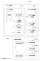
- FIG. 1 is a block diagram showing a configuration example of a detection system according to the present technology, and is a block diagram showing the configuration of a detection system according to first and second embodiments.
- FIG. 1 is a diagram showing an overview of a detection system.
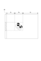
- 11A and 11B are diagrams illustrating an example of determining whether or not a target subject is captured for each pixel block region.
- 11 is a diagram for explaining a change in average luminance value between frames in a pixel block region in which a target subject is imaged;
- FIG. FIG. 13 is a diagram showing an example of additional information for each line.
- FIG. 11 is a diagram illustrating an example of a data structure of output data. A diagram showing the data structure of packet data that complies with the SLVS-EC standard.
- FIG. 11 is a diagram for explaining that multiple pixel data are stored in a payload area in packet data.
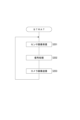
- FIG. 10 is a flowchart showing an example of processing executed by the detection system regarding detection of a target subject, generation of additional information, etc.; 13 is a flowchart illustrating an example of a process executed by a sensor outside processing unit.
- 10 is a flowchart illustrating an example of a process executed by the detection system for identifying a region to be processed and image processing.
- 13 is a diagram for explaining an example in which a valid range and an invalid range are further set in the valid line data.
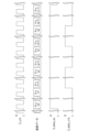
- FIG. FIG. 13 is a diagram showing an example of a signal that is output to distinguish between a valid range and an invalid range.
- 11A and 11B are diagrams for explaining a processing target area that is set as a range to be processed in subsequent image processing.
- FIG. 13 is a block diagram showing a configuration of a detection system according to a third embodiment.
- a sensor device 1 according to a first embodiment of the present technology will be described.
- the sensor device 1 is included in a camera device 2, and constitutes a detection system S together with a downstream information processing device 3.
- the detection system S detects a subject to be detected in an image obtained by imaging, determines an area to be processed in subsequent image processing, and performs image processing on a portion of the frame image FG based on the subject detection result and the determined area.
- the detection system S is applied to, for example, a system for detecting defects in a product, or a system for reading a one-dimensional code or a two-dimensional code affixed to a subject.
- the detection system S includes a camera device 2 and an information processing device 3 (see Figures 1 and 2).
- the camera device 2 is equipped with a sensor device 1 and a downstream external processing unit 4.
- the sensor device 1 is configured as, for example, a CCD (Charge Coupled Device) type or CMOS (Complementary Metal Oxide Semiconductor) type image sensor, and includes an imaging unit 5, a detection processing unit 6, an additional information generating unit 7, an output data generating unit 8, and an output unit 9.
- CCD Charge Coupled Device
- CMOS Complementary Metal Oxide Semiconductor
- the imaging unit 5 includes a pixel array section 5a in which pixels having photoelectric conversion elements such as photodiodes as light receiving sections are arranged two-dimensionally, and a readout circuit that reads out electrical signals obtained by photoelectric conversion from each pixel in the pixel array section 5a, and is capable of outputting the electrical signals as imaging data in the form of RAW data.
- a pixel array section 5a in which pixels having photoelectric conversion elements such as photodiodes as light receiving sections are arranged two-dimensionally, and a readout circuit that reads out electrical signals obtained by photoelectric conversion from each pixel in the pixel array section 5a, and is capable of outputting the electrical signals as imaging data in the form of RAW data.
- the imaging data output from the imaging unit 5 is, for example, data for each line that combines data for multiple pixels included in the same row (line). This data for each line is referred to as “line data LD.” Note that data for one pixel included in the line data LD may also be referred to as "pixel data.”
- the line data LD output from the pixel array unit 5a may be not only data such as color images or monochrome images, but also two-dimensional data having values for each pixel, such as distance images, EVS data, heat map images, spectral images, and polarized images.
- the image processing unit at the subsequent stage can perform image processing to inspect the quality of the product based on imaging data such as color images or monochrome images. Also, the image processing unit at the subsequent stage can perform image processing to detect defects in the shape of the product (holes, chips, etc.) based on imaging data as a distance image. Furthermore, the image processing unit at the subsequent stage can perform image processing to detect the degree of doneness of the food product based on imaging data as a heat map image.
- image processing in a downstream image processing unit based on imaging data such as spectral images and polarized images to detect defects in the color of the product.
- imaging data such as spectral images and polarized images
- the subsequent image processing unit is provided in an information processing device 3 provided outside the camera device 2.
- the readout circuit provided in the pixel array unit 5a performs, for example, CDS (Correlated Double Sampling) processing, AGC (Automatic Gain Control) processing, etc. on the electrical signal obtained by photoelectric conversion, and further performs A/D (Analog/Digital) conversion processing.
- CDS Correlated Double Sampling
- AGC Automatic Gain Control
- A/D Analog/Digital
- the imaging data after A/D conversion is output to the detection processing unit 6.
- the imaging data provided to the detection processing unit 6 is digital data (RAW data) that has been subjected to A/D conversion processing and is output from the imaging unit 5.
- RAW data digital data
- data that has been subjected to preprocessing or the like on the RAW data may be provided to the detection processing unit 6.
- Pre-processing involves clamping the R, G, and B black levels of the captured image data to a specified level, as well as correction between the R, G, and B color channels.
- the detection processing unit 6 performs processing to detect the target subject OB that is the subject of subsequent image processing for each line data LD.
- the detection processing unit 6 may divide data (frame image FG as RAW data) obtained by collecting each line data LD into one frame of image data into pixel block regions Ar, and detect the target subject OB for each pixel block region Ar.
- the additional information generating section 7 Based on the detection result of the detection processing section 6, the additional information generating section 7 generates additional information AD for each line data LD, which indicates whether or not the target subject OB is included.
- the determination result as the additional information AD can be expressed by 1-bit flag information.
- the output data generation unit 8 uses the line data LD and additional information AD to generate output data OD to be output to a downstream processing unit.
- the generated output data OD may be, for example, data that conforms to the SLVS (Scalable Low Voltage Signaling) standard (including SLVS-EC (SLVS with Embedded Clock)), data that conforms to the MIPI (Mobile Industry Processor Interface) standard, or data that has a different configuration.
- SLVS Scalable Low Voltage Signaling
- MIPI Mobile Industry Processor Interface
- the output unit 9 outputs the output data OD generated by the output data generation unit 8 to a subsequent processing unit, specifically, the sensor external processing unit 4.
- the output data OD output from the output unit 9 to the outside of the sensor device 1 is data that includes one line of line data LD and its additional information AD. In other words, the output unit 9 outputs the same number of output data OD as the number of line data LD for one frame of imaging.
- the sensor external processing unit 4 is configured with a sensor image receiving unit 10, a camera signal processing unit 11, and a camera image transmitting unit 12.
- the sensor image receiving unit 10 receives output data OD as a sensor image output from the sensor device 1 and supplies it to the downstream camera signal processing unit 11.
- the camera signal processing unit 11 performs development processing, including the pre-processing, synchronization processing, and YC generation processing, described above, on the sensor image output from the sensor device 1. Furthermore, the development processing may include resolution conversion processing, codec processing, and the like, as necessary.
- a color separation process is performed so that the image data for each pixel contains all the R, G, and B color components.
- a demosaic process is performed as the color separation process.
- YC generation process a luminance (Y) signal and a chrominance (C) signal are generated (separated) from the R, G, and B image data.
- C chrominance
- a resolution conversion process is performed on the image data that has been subjected to various signal processes.
- codec processing the imaging data that has been subjected to the various processes described above is encoded and files are generated for recording or communication, for example.
- codec processing it is possible to generate video file formats such as MPEG-2 (Moving Picture Experts Group) and H.264. It is also possible to generate still image file formats such as JPEG (Joint Photographic Experts Group), TIFF (Tagged Image File Format), and GIF (Graphics Interchange Format).
- the camera image transmission unit 12 performs processing to transmit the image data (camera image data) obtained by processing of the camera signal processing unit 11 to a device external to the camera device 2.
- the camera image transmission unit 12 transmits the camera image data to the information processing device 3 provided in the detection system S.
- the information processing device 3 performs a predetermined image processing on the camera image data received from the camera device 2. At this time, the information processing device 3 selects a part of the camera image data and performs the image processing.
- the information processing device 3 includes a reception processing unit 13, a determination processing unit 14, an image processing unit 15, a storage processing unit 16, and a display processing unit 17.
- the reception processing unit 13 receives camera image data from the camera device 2.
- the received camera image data is supplied to the storage processing unit 16 and stored in a storage unit (not shown).
- the received camera image data is also supplied to the determination processing unit 14.
- the determination processing unit 14 uses the additional information AD for each line data LD related to the supplied camera image data to determine the lines to be processed. In other words, the determination processing unit 14 determines whether or not image processing can be performed for each line data LD in the camera image data.
- the determination result is supplied to the image processing unit 15 together with the camera image data.
- the image processing unit 15 performs image processing on the processing target area (line) in the camera image data based on the determination result of the determination processing unit 14 .
- the image processing executed by the image processing unit 15 includes, as described above, the process of detecting the target subject OB and determining whether or not there is a defect or other problem, and the process of detecting and reading a two-dimensional code as the target subject OB.
- the image processing unit 15 performs image processing on the line data LD that is determined to be the subject of image processing based on the additional information AD. In other words, the image processing unit 15 does not perform image processing on the line data LD that is determined not to be the subject of image processing based on the additional information AD.
- the results of processing by the image processing unit 15 are supplied to the memory processing unit 16 and stored in a memory unit (not shown).
- the image processing unit 15 supplies the result of the image processing to the display processing unit 17. This makes it possible to present the result of the image processing to the user who is using the detection system S.
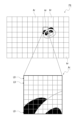
- FIG. 3 shows an image of a target subject OB traveling on a conveyor belt captured by the camera device 2 shown in FIG. 2, and shows a frame image FG generated from one frame of line data LD output from the imaging unit 5.
- the detection processing unit 6 divides the frame image FG into multiple pixel block regions Ar and detects the target subject OB for each pixel block region Ar.
- the detection processing unit 6 defines the pixel block regions Ar in which the target subject OB is captured as "valid blocks Bv" and the pixel block regions Ar in which the target subject OB is not captured as "invalid blocks Bi.”
- the detection processing unit 6 judges valid blocks Bv and invalid blocks Bi using the average luminance value calculated for each pixel block region Ar.
- One pixel block area Ar is, for example, an area of 64 pixels in total, consisting of 8 pixels vertically and horizontally.
- the detection processing unit 6 detects the target subject OB when one frame's worth of line data LD is received from the imaging unit 5, or when the amount of line data LD that can be processed for the pixel block area Ar is received from the imaging unit 5. That is, in the example shown in FIG. 3, the detection process may be executed every time all of the line data LD contained in the frame image FG is received, or every time eight pieces of line data LD are received.
- the detection processing unit 6 compares the average brightness value calculated for the pixel block region Ar with a threshold value, and if the deviation between the average brightness value and the reference value is greater than or equal to a predetermined value, it determines that the target subject OB has been detected and determines that the pixel block region Ar is a valid block Bv.
- the reference value used for comparison with the average brightness value may be the average brightness value of the pixel block area Ar in which only the conveyor belt is shown.
- the reference value may be different for each pixel block area Ar.
- a reference value may be set for each pixel block region Ar using a frame image FG captured when no goods or products are being conveyed on the belt conveyor.
- the line data LD including a part of one effective block Bv is eight line data LD. These eight line data LD are set as "effective line data LDv" which is the line data LD to be subjected to the subsequent image processing.
- the additional information generating unit 7 sets a validity flag Fv as additional information AD for each of these valid line data LDv.
- the detection processing unit 6 determines the valid blocks Bv and the invalid blocks Bi.
- the effective blocks Bv may be determined based on the change in average luminance value between the previous frame image FG and the current frame image FG.
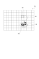
- Figure 4 shows the current frame image FG, and the position of the target subject OB in the previous frame image FG is indicated by a dashed line.
- Pixel block area Ar1 is one of the pixel block areas Ar in which part of the target subject OB was captured in the previous frame image.
- Pixel block area Ar2 is one of the pixel block areas Ar in which part of the target subject OB was captured in the current frame image FG.
- both pixel block regions Ar1 and Ar2 are pixel block regions Ar whose average luminance value has changed. Therefore, the detection processing unit 6 may determine that both pixel block regions Ar1 and Ar2 are valid blocks Bv.
- the detection processing unit 6 may determine the effective block Bv based on the direction of change of the average luminance value. For example, consider a case where the target subject OB is a subject with a luminance value greater than black. In this case, by changing the color of the conveyor belt to black, the pixel block area Ar2 in which the target subject OB is not reflected in the pixel block area Ar2 is changed to a state in which the target subject OB is reflected in the pixel block area Ar2, and the change in the average luminance value is determined to be in the positive direction.
- the change in the average luminance value is in the negative direction. Therefore, by determining the pixel block area Ar in which the average brightness value has changed in the positive direction as the effective block Bv, it is possible to determine only the line data LD in which the target subject OB is imaged as the effective line data LDv to be processed.
- the color of the conveyor belt is configured to be white, and the pixel block area Ar where the average brightness value has changed in the negative direction is determined to be the effective block Bv, making it possible to set appropriate additional information AD.
- the frame image FG used in the detection processing unit 6 is raw data before the synchronization process. Therefore, when the color of the target subject OB is red, it is possible to appropriately determine the effective block Bv by calculating the change in the average brightness value of red in the pixel block area Ar. In this case, it is desirable to set the color of the conveyor belt so that the brightness value of red when the conveyor belt is imaged is different from the brightness value of red when the target subject OB is imaged.
- the detection result of the target subject OB for each line data LD is added to the line data LD as additional information AD.
- the additional information AD is information indicating the presence or absence of detection and can be expressed by 1-bit flag information.
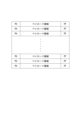
- the additional information AD is shown in Fig. 5.
- the hatched rows are rows in which "1", indicating that the row is valid line data LDv, is set as the additional information AD.
- the non-hatched rows are rows in which "0”, indicating invalid line data LDi, is set as the additional information AD.
- this additional information AD which is 1-bit flag information
- the packet data for transmitting the line data LD it is possible to communicate to a downstream processing unit whether or not the line data LD is to be subjected to image processing.
- each packet is provided with a packet header PH, a payload area, and a packet footer PF.
- the payload area in one packet contains, for example, one line data LD.
- the configuration of the packet header PH varies depending on the specifications.
- the packet header PH includes "Frame Start”, “Frame End”, “Line Valid”, “Line Number”, “EBD Line”, “Data ID”, “Header Info Type”, “Reserved”, “Line Length”, “Reserved”, and “ECC” (see Figure 7).
- the additional information AD may be stored in an area such as "Word Count". Since the information in "Word Count" is unnecessary information since the packet size when transmitting one piece of line data LD is also known if the size of the pixel array unit 5a is known, it is possible to store the additional information AD instead.
- the additional information AD which is 1-bit flag information, can be stored in an area in the packet data separate from the area in the line data LD.
- the additional information AD may be included in the line data LD.
- the line data LD contains n pieces of pixel data (see FIG. 8).
- pixel data (0) indicates that this is the first (first) pixel data
- pixel data (n-1) indicates that this is the nth (last) pixel data.
- the pixel data at both ends of the line data LD is replaced with the additional information AD. More preferably, the pixel data at the beginning of the line data LD is replaced with the additional information AD.
- the first pixel (the pixel at the left end horizontally) and the last pixel (the pixel at the right end horizontally) are pixels that are unlikely to contain the target subject if the angle of view of the camera device 2 is set appropriately. Therefore, by replacing the pixel data of such edge pixels among the pixel data contained in the line data LD with additional information AD, it is possible to transmit both the line data LD and the additional information AD without changing the packet size while maintaining the effectiveness of the image processing at the subsequent stage.
- one bit in the pixel data of the first pixel or the last pixel may be treated as the additional information AD.
- the LSB in the pixel data may be assigned to the additional information AD. This makes it possible to minimize the effect on the pixel data of the first pixel or the last pixel, and to treat the pixel data as the original pixel data.
- FIG. 9 shows an example of a process executed by the sensor device 1 in the camera device 2
- FIG. 10 shows an example of a process executed by the outside-sensor processing unit 4 in the camera device 2.
- FIG. 11 shows an example of processing executed by the information processing device 3, which is a device downstream of the camera device 2.
- FIG. 9 and FIG. 10 are executed for each capture of a frame image FG, which is repeated from when the detection system S starts to operate until it stops operating.
- FIG. 11 shows a process that is repeated from when the detection system S starts to operate until it stops operating, and is executed multiple times for each capture of a frame image FG, equal to the number of line data LD.
- the imaging unit 5 of the sensor device 1 of the camera device 2 performs imaging processing in step S101 of FIG. 9.
- the detection processing unit 6 of the sensor device 1 After completing the imaging process, the detection processing unit 6 of the sensor device 1 performs a target subject detection process in step S102.
- the process of detecting the target subject OB is performed for each pixel block region Ar based on the average luminance value, for example, as described above.
- the additional information generating unit 7 of the sensor device 1 performs a process to generate additional information AD in step S103.
- step S104 the output data generation unit 8 of the sensor device 1 generates output data (packet data, which is data of the sensor image) using the line data LD and the additional information AD.
- step S105 the output unit 9 of the sensor device 1 outputs the output data to the downstream external processing unit 4.
- the sensor image receiving unit 10 of the outside-sensor processing unit 4 of the camera device 2 receives the sensor image in step S201 of FIG. 10.
- the camera signal processing unit 11 of the sensor outside processing unit 4 performs signal processing in step S202.
- This signal processing may be the synchronization processing or YC generation processing described above.
- the camera image transmission unit 12 of the sensor external processing unit 4 transmits the camera image to the information processing device 3, which is the downstream device, in step S203.
- the reception processing unit 13 of the information processing device 3 performs a process of receiving this camera image in step S301 of FIG. 11. Specifically, data including one line data LD in the camera image is received.
- the determination processing unit 14 of the information processing device 3 extracts the additional information AD corresponding to the line data LD received in step S302, and determines whether the received line data LD is valid line data LDv.
- step S303 the information processing device 3 performs branching processing based on the determination result of the additional information AD. Specifically, if the additional information AD indicates valid line data LDv, the image processing unit 15 of the information processing device 3 performs image processing in step S304. As described above, this image processing includes processing to detect the target subject OB and determine whether or not there is a defect or other problem, and processing to detect and read a two-dimensional code as the target subject OB.
- step S304 may be executed, for example, after waiting until a series of pixel data is accumulated. 5 as an example, in the case where two target subjects OB are captured in the frame image FG, after a plurality of line data LD in which one target subject OB is captured is received, the image processing of step S304 is performed on the area represented by the plurality of line data LD. Then, after a plurality of line data LD in which the other subject OB is captured is received, the image processing of step S304 is performed again on the area represented by the plurality of line data LD.
- image processing in step S304 may be performed after all valid line data LDv in one frame image FG has been received.
- step S305 the storage processing unit 16 of the information processing device 3 performs processing to store the results of the image processing.
- step S306 the display processing unit 17 of the information processing device 3 performs display processing of the result of the image processing and the frame image FG.
- the information processing device 3 discards the line data LD received in step S307, or performs processing to use it as complementary information in the image processing of step S305 executed on the valid line data LDv.
- the process for using the received invalid line data LDi as complementary information is, for example, a process for storing the received invalid line data LDi in a storage unit.
- Second embodiment The configuration of a camera device 2A of a detection system SA in the second embodiment is similar to that of the camera device 2 shown in Fig. 1. Therefore, only the different parts will be described to avoid redundant description.
- the camera device 2A includes a sensor device 1A and an external processing unit 4A.
- the detection processing unit 6A of the sensor device 1A not only determines whether each line data LD contains pixel data of an image of a target subject OB that is to be subjected to subsequent image processing, but also determines the range of the line data LD that is to be subjected to image processing as a valid range Rv and the range that is not to be subjected to image processing as an invalid range Ri.
- the additional information AD for distinguishing between valid line data LDv and invalid line data LDi for each line data LD is generated by the additional information generating unit 7 . Furthermore, the detection processing unit 6A sets the pixel range in which the target subject OB in the effective line data LDv is imaged as the effective range Rv, and sets the pixel range in which the target subject OB is not imaged as the invalid range Ri.
- the valid range Rv and invalid range Ri are different for each line data LD. Also, the valid range Rv is not set for invalid line data LDi.
- valid range Rv and invalid range Ri may be set for each pixel block region Ar described above.
- the sensor device 1A outputs to the sensor outside processing unit 4A information for identifying the valid range Rv and the invalid range Ri together with the line data LD and the additional information AD.
- the information for identifying the valid range Rv and the invalid range Ri may be, for example, information for identifying the pixel at the boundary between the valid range Rv and the invalid range Ri, information indicating the pixel block area Ar that belongs to the valid range Rv (or the invalid range Ri), or information indicating the start pixel of the valid range Rv and the number of pixels included in the valid range Rv.
- a synchronization signal synchronized with the transmission of the line data LD is supplied from the sensor device 1A to the outside-sensor processing unit 4A.
- the sensor outside processing unit 4A is capable of determining the valid range Rv and the invalid range Ri in the line data LD based on the received synchronization signal.
- the output unit 9 of the sensor device 1A outputs a pixel clock signal S_clk, packet data, a pixel data enable signal S_data_en, and a valid data signal S_data_vld to the outside-sensor processing unit 4A.
- Fig. 13 is a timing chart showing a period during which pixel data of the packet data is being transmitted.
- the line data LD contains n pixel data. Each pixel data is shown in the figure as Pix(0) to Pix(n-1).
- the valid range Rv in the line data LD is the range from Pix(f+1) to Pix(g) and the range from Pix(h+1) to Pix(m). That is, the invalid ranges Ri are the range from Pix(0) to Pix(f), the range from Pix(g+1) to Pix(h), and the range from Pix(m+1) to Pix(n-1).
- the pixel data enable signal S_data_en is set to 1 (High), and the rest is set to 0 (Low).
- the valid data signal S_data_vld is set to 1 (High)
- the valid data signal S_data_vld is set to 0 (Low).
- the sensor image receiving unit 10 of the sensor outside processing unit 4A receives the pixel clock signal S_clk, pixel data enable signal S_data_en, and valid data signal S_data_vld along with the packet data, and obtains the line data LD and additional information AD.
- the line data LD and additional information AD obtained here are provided to the information processing device 3A via the camera image transmitting unit 12A.
- the receiving processing unit 13A of the information processing device 3A provides the received line data LD and additional information AD to the storage processing unit 16, and further provides information about the effective range Rv in the line data LD to the storage processing unit 16.
- reception processing unit 13A supplies the line data LD, additional information AD, and information specifying the valid range Rv to the determination processing unit 14A.
- the determination processing section 14A determines the lines to be subjected to image processing using the additional information AD for each line data LD related to the supplied camera image data. Furthermore, the determination processing section 14A determines the effective range Rv of the effective line data LDv. That is, the determination processing unit 14A performs processing to specify a rectangular processing target area ArT that is to be the target of subsequent image processing (see FIG. 14).
- the image processing unit 15A obtains the desired results by performing image processing on the processing target area ArT identified by the judgment processing unit 14A. In other words, the image processing unit 15A does not perform image processing on the invalid line data LDi or image processing on the invalid range Ri in the valid line data LDv.
- the results obtained by the image processing are provided to the storage processing unit 16 and the display processing unit 17, where they are stored and presented to the user.
- the image processing unit 15 that performs predetermined image processing is provided in the information processing device 3 (3A) downstream of the camera device 2 (2A).
- the camera device 2B includes an image processing unit 15B.
- a configuration example of the detection system SB is shown in Fig. 15. Note that the same components as those in the first and second embodiments are given the same reference numerals and the description thereof will be omitted as appropriate.
- the detection system SB includes a camera device 2B and an information processing device 3B.
- the information processing device 3B is a device for presenting the image processing results to the user.
- the camera device 2B includes a sensor device 1 and an external processing unit 4B.
- the sensor device 1 comprises an imaging section 5, a detection processing section 6, an additional information generating section 7, an output data generating section 8, and an output section 9.
- the configuration of each section is the same as in the first embodiment. That is, the sensor device 1 outputs output data OD (sensor image data) that conforms to a predetermined standard and includes line data LD and additional information AD.
- the sensor external processing unit 4B includes a sensor image receiving unit 10B, a judgment processing unit 14B, an image processing unit 15B, and an information transmission unit 18.
- the sensor image receiving unit 10B receives the output data OD output from the sensor device 1 and supplies it to the downstream determination processing unit 14B.
- the determination processing unit 14B determines the valid line data LDv that is to be subjected to image processing using the additional information AD for each line data LD related to the supplied sensor image.
- the determination processing section 14B supplies information on the valid line data LDv to the downstream image processing section 15B to prompt the image processing of the valid line data LDv.
- the image processing unit 15B obtains a desired result by performing image processing on the valid line data LDv specified by the determination processing unit 14B, and avoids image processing on the invalid line data LDi.
- the invalid line data LDi that is not the target of image processing may be discarded by the determination processing unit 14B or may be used as complementary data for the image processing of the valid line data LDv.
- the processing results by the image processing unit 15B and partial image data for the valid line data LDv that was the subject of processing are sent to the information sending unit 18.
- the information transmission unit 18 transmits the information received from the image processing unit 15B to the information processing device 3B. Note that the information transmission unit 18 may transmit the entire sensor image relating to the frame to the information processing device 3B.
- the information processing device 3B includes a reception processing unit 13, a storage processing unit 16, and a display processing unit 17.
- the reception processing unit 13 supplies partial image data and information on the results of image processing for the valid line data LDv received from the camera device 2B to the storage processing unit 16, thereby storing the information in the storage unit.
- the reception processing unit 13 also supplies the information received from the camera device 2B to the display processing unit 17, thereby realizing a process of presenting the information to the user.
- the process flow in the third embodiment will be described.
- the sensor device 1 of the camera device 2B executes the processes from step S101 to step S105 shown in FIG. 9 to detect the target subject OB, generate additional information AD, generate output data OD, etc.
- outside-sensor processing unit 4B of the camera device 2B performs image processing on a partial area of the frame image FG by performing the processes of steps S301, S302, S303, S304, and S307 shown in FIG. 11.
- the information processing device 3B executes the processes of steps S305 and S306 shown in FIG. 11, thereby performing the process of storing information and the process of presenting information to the user.
- the detection system S (SA, SB) in the above-mentioned example performs processing to determine the area to be processed inside the sensor device 1 (1A). Therefore, the data output from the sensor device 1 (1A) may be only pixel data of the range determined as the effective line data LDv or the effective range Rv of the frame image FG. This reduces the amount of communication traffic required for sending and receiving pixel data, thereby enabling a reduction in the processing load and effective use of communication bandwidth.
- the camera device 2 and the information processing device 3 are described as separate devices, but other configurations are also possible.
- the camera device 2 may be configured as a camera module equipped with a sensor device 1 and an extra-sensor processing unit 4
- the information processing device 3 may be configured as an extra-module processing unit provided outside the camera module, and the camera module and the extra-module processing unit may be provided within a single device.
- the sensor device 1 (1A) comprises a pixel array section 5a in which pixels are arranged two-dimensionally, a detection processing section 6 (6A) that determines whether each line data LD output from the pixel array section 5a is valid line data LDv to be processed in subsequent image processing, an additional information generation section 7 that generates additional information AD based on the result of the determination by the determination processing section (detection processing sections 6, 6A), an output data generation section 8 that generates output data OD for each line using the line data LD and the additional information AD, and an output section 9 that outputs the output data OD.
- a detection processing section 6 (6A) that determines whether each line data LD output from the pixel array section 5a is valid line data LDv to be processed in subsequent image processing
- an additional information generation section 7 that generates additional information AD based on the result of the determination by the determination processing section (detection processing sections 6, 6A)
- an output data generation section 8 that generates output data OD for each line using the line data LD and the
- the downstream image processing unit 15 15A, 15B. Therefore, image processing of the invalid line data LDi can be avoided, and the processing load can be reduced. Also, by performing image processing only on the valid line data LDv, it becomes easy to handle output at a high frame rate, and suitable image processing of a subject (target subject OB) moving at high speed can be realized.
- the camera device 2 (2A, 2B) including the above-mentioned sensor device 1 (1A) can also be considered as the sensor device of the present technology.
- the additional information AD may be flag information for each line data LD. This minimizes the amount of data in the additional information AD, thereby preventing an increase in the amount of data in the output data OD and reducing the processing load on the downstream image processor 15 (15A, 15B).
- the output data generation unit 8 in the sensor device 1 (1A) may generate output data OD by storing additional information AD in an area (e.g., a packet header area) other than the area (e.g., a payload area) in which the line data LD is stored.
- additional information AD in an area (e.g., a packet header area) other than the area (e.g., a payload area) in which the line data LD is stored.
- the output data generation unit 8 in the sensor device 1 (1A) may adopt a header area (header area of packet data) as the separate area in which additional information AD is stored. This makes it possible to transmit the additional information AD without increasing the size of the payload area in which the line data LD is stored. Furthermore, by storing the additional information AD in an unused area or an extension area in the header area, it is possible to suppress an increase in the data size of the packet data without the need to change the header size.
- the output data generating unit 8 in the sensor device 1 (1A) may generate the output data OD by including additional information AD in a part of the line data LD. This makes it possible to transmit both the line data LD and the additional information AD without changing the configuration of the header or the configuration of the payload area.
- the output data generating unit 8 in the sensor device 1 (1A) may include additional information AD in the pixel data of the leading pixel in the line data LD.
- the pixel data of the leading pixel is pixel data that is highly likely not an image of the target subject OB.
- the additional information AD may be included in the pixel data of the last pixel in the line data LD.
- additional information AD in the pixel data of the leading pixel, it is possible to determine whether or not the remaining data of the line data LD is unnecessary at the stage when the leading portion of the line data LD is read. Therefore, the processing load associated with the analysis of the line data LD can be reduced.
- additional information AD flag information consisting of one bit, only one bit of information in the pixel data is used as flag information, so that the influence on the image can be reduced.
- LSB Location Significant Bit
- the judgment processing unit (detection processing units 6, 6A) in the sensor device 1 (1A) judges the valid range Rv and invalid range Ri in the line data LD judged to be valid line data LDv, and the output unit 9 may output a first synchronization signal (pixel data enable signal S_data_en) synchronized with the line data LD in the output data OD, and a second synchronization signal (valid data signal S_data_vld) synchronized with the output timing of the data of the valid range Rv and invalid range Ri.
- a first synchronization signal pixel data enable signal S_data_en
- a second synchronization signal valid data signal S_data_vld
- the downstream image processing unit 15 (15A, 15B) can identify the valid range Rv and the invalid range Ri in the line data LD based on the input second synchronization signal (valid data signal S_data_vld). Therefore, image processing can be performed more efficiently.
- the judgment processing unit (detection processing unit 6, 6A) in the sensor device 1 (1A) may determine whether or not each pixel block area Ar consisting of a plurality of pixels in the row and column directions is an effective block Bv that will be subject to subsequent image processing, and may determine that line data LD containing a portion of the effective block Bv is effective line data LDv. This allows the determination of validity/invalidity to be performed with higher accuracy than if it were performed for each line, and therefore reduces the possibility of unnecessary image processing being performed in the downstream image processing unit 15 (15A, 15B), thereby reducing the processing load.
- the judgment processing unit (detection processing unit 6, 6A) in the sensor device 1 (1A) may calculate the average luminance value of the pixel block area Ar and make a judgment about the effective block Bv.
- the average brightness value for a pixel block area Ar in which the product is captured differs from the average brightness value for a pixel block area Ar in which only the conveyor belt is captured. Therefore, it is possible to distinguish the pixel block area Ar to be processed by simple processing, which makes it possible to perform efficient image processing in the downstream image processing unit 15 (15A, 15B) while suppressing an increase in the processing load on the sensor device.
- the judgment processing unit (detection processing unit 6, 6A) in the sensor device 1 (1A) may calculate the change in average luminance value between frames and make a judgment about the effective block Bv.
- the pixel block area Ar in which the average luminance value has changed is determined to be a valid block Bv. Therefore, it is possible to realize efficient detection of the valid block Bv.
- the judgment processing unit (detection processing unit 6, 6A) in the sensor device 1 (1A) may judge the pixel block area Ar to be an effective block Bv when the change in the calculated average luminance value between frames is a change in a predetermined direction.
- the direction of change can be a positive direction in which the luminance value increases, or a negative direction in which the luminance value decreases.
- the direction of change for a pixel block area Ar into which a product is newly captured is the positive direction in which the luminance value increases
- the direction of change for a pixel block area Ar which has changed to a state in which only the conveyor belt is captured after the product has passed is the negative direction in which the luminance value decreases.
- the effective block Bv that is the target of image processing by the downstream image processing unit 15 (15A, 15B) is the pixel block area Ar in which a positive change in luminance value increase is observed.
- the pixel block area Ar that is subject to subsequent image processing can be reduced, thereby making it possible to reduce the processing burden.
- the same effect can be obtained by setting the pixel block area Ar in which the direction of change in the average brightness value is negative as the effective area.
- the judgment processing unit (detection processing unit 6, 6A) in the sensor device 1 (1A) may determine the effective range Rv and the invalid range Ri in the line data LD that has been determined to be valid line data LDv, and may determine the range of the valid line data LDv that is included in the effective block Bv as the effective range Rv.
- the data structure of the present technology is a data structure of output data OD output from a sensor device 1 (1A) having a pixel array section 5a in which pixels are arranged two-dimensionally, and is generated based on line data LD output from the pixel array section 5a and additional information AD that indicates the determination result of whether or not each line data LD is valid line data LDv that will be processed in subsequent image processing.
- the information processing device 3 (3A) of the present technology or the sensor outside processing unit 4B as an information processing device includes a reception processing unit 13, 13A (or a sensor image receiving unit 10B) that receives output data OD generated based on line data LD output from a pixel array unit 5a in which pixels are arranged two-dimensionally and additional information AD indicating a judgment result as to whether or not each line data LD is valid line data LDv to be processed in subsequent image processing from the sensor device 1 (1A), a judgment processing unit 14 (14A, 14B) that determines whether or not a predetermined image processing can be performed on the line data LD based on the additional information AD included in the output data OD received by the reception processing unit 13, 13A (or the sensor image receiving unit 10B), and an execution processing unit (image processing unit 15, 15A, 15B) that executes a predetermined image processing on the line data LD based on the judgment result of the judgment processing unit 14 (14A, 14B).
- a reception processing unit 13, 13A or a sensor image
- the execution processing unit (image processing units 15, 15A, 15B) in the information processing device 3 (3A) of the present technology or the sensor-external processing unit 4B as an information processing device does not need to perform a predetermined image processing on the line data LD when it is determined that the line data LD is not valid line data LDv based on the additional information AD corresponding to the line data LD.
- This makes it possible to limit the data that is the subject of image processing to a portion, thereby reducing the processing load on the information processing device.
- by performing image processing only on the effective line data LDv it becomes easy to support output at a high frame rate, and suitable image processing for a subject that moves at high speed can be realized.
- the information processing device 3 (3A) of the present technology or the judgment processing unit 14 (14A, 14B) of the sensor outside processing unit 4B as an information processing device may discard the line data LD when it determines that the line data LD is not valid line data LDv based on the additional information AD corresponding to the line data LD. This allows only a portion of the line data LD to be stored, thereby enabling efficient use of the storage area.
- the present technology can also be configured as follows. (1) a pixel array section in which pixels are arranged two-dimensionally; a determination processing unit that determines whether each line data output from the pixel array unit is valid line data to be processed in a subsequent image processing stage; an additional information generating unit that generates additional information based on a result of the determination by the determination processing unit; an output data generation unit that generates output data for each line by using the line data and the additional information; and an output unit that outputs the output data. (2) The sensor device according to (1), wherein the additional information is flag information for each of the line data.
- the determination processing unit determines a valid range and an invalid range in the line data determined to be the valid line data, The sensor device described in any of (1) to (6) above, wherein the output unit outputs a first synchronization signal synchronized with the line data in the output data and a second synchronization signal synchronized with the output timing of the data of the valid range and the invalid range.
- the judgment processing unit judges whether each pixel block area consisting of a plurality of pixels in the row and column directions is an effective block to be processed in the subsequent image processing, and judges the line data including a portion of the effective block to be the effective line data.A sensor device described in any of (1) to (7) above.
- a reception processing unit that receives output data from a sensor device, the output data being generated based on line data output from a pixel array unit in which pixels are two-dimensionally arranged and additional information indicating a determination result as to whether each of the line data is valid line data to be processed in a subsequent image processing stage; a determination processing unit that determines whether or not a predetermined image processing can be performed on the line data based on the additional information included in the output data received by the reception processing unit; an image processing unit that executes the predetermined image processing on the line data based on a determination result of the determination processing unit.
Landscapes
- Engineering & Computer Science (AREA)
- Multimedia (AREA)
- Signal Processing (AREA)
- Computer Vision & Pattern Recognition (AREA)
- Physics & Mathematics (AREA)
- General Physics & Mathematics (AREA)
- Theoretical Computer Science (AREA)
- Studio Devices (AREA)
Abstract
センサ装置は、画素が2次元配列された画素アレイ部と、前記画素アレイ部から出力されるラインデータごとに後段の画像処理の処理対象とされる有効ラインデータであるか否かを判定する判定処理部と、前記判定処理部による前記判定の結果に基づいて付加情報を生成する付加情報生成部と、前記ラインデータと前記付加情報とを用いてラインごとの出力データを生成する出力データ生成部と、前記出力データを出力する出力部と、を備える。
Description
本技術は、画素アレイ部から出力されるラインごとのデータについてのセンサ装置、データ構造、情報処理装置の技術に関する。
画像データに対する画像処理を行うことにより被写体検出や欠陥検出などを行うシステムが知られている。このようなシステムでは、画像処理を効率よく行うことが必要とされる場合がある。
例えば、下記特許文献1においては、画像データに画像のシフト方向を示すフラグを付加する技術が開示されている。
例えば、下記特許文献1においては、画像データに画像のシフト方向を示すフラグを付加する技術が開示されている。
ところで、30fpsや60fpsを超える高速なイメージセンサが普及してきている。このような高速出力される画像データとしてのフレーム画像に対して画像処理を行う場合には、画像処理における演算量を減らすことが望ましい。
本技術はこのような問題に鑑みて為されたものであり、フレーム画像に対する画像処理の処理負担軽減を図ることを目的とする。
本技術に係るセンサ装置は、画素が2次元配列された画素アレイ部と、前記画素アレイ部から出力されるラインデータごとに後段の画像処理の処理対象とされる有効ラインデータであるか否かを判定する判定処理部と、前記判定処理部による前記判定の結果に基づいて付加情報を生成する付加情報生成部と、前記ラインデータと前記付加情報とを用いてラインごとの出力データを生成する出力データ生成部と、前記出力データを出力する出力部と、を備えたものである。
これにより、後段の情報処理装置においてラインデータごとに画像処理を行うか否かを決定することができる。
これにより、後段の情報処理装置においてラインデータごとに画像処理を行うか否かを決定することができる。
本技術に係るデータ構造は、画素が2次元配列された画素アレイ部を有するセンサ装置から出力される出力データのデータ構造であって、前記画素アレイ部から出力されるラインデータと、前記ラインデータごとに後段の画像処理の処理対象とされる有効ラインデータであるか否かの判定結果を示す付加情報と、に基づいて生成されるものである。
本技術に係る情報処理装置は、画素が2次元配列された画素アレイ部から出力されるラインデータと、前記ラインデータごとに後段の画像処理の処理対象とされる有効ラインデータであるか否かの判定結果を示す付加情報と、に基づいて生成される出力データをセンサ装置から受信する受信処理部と、前記受信処理部によって受信した前記出力データに含まれる前記付加情報に基づいて、前記ラインデータに対する所定の画像処理の実行可否を決定する判定処理部と、前記判定処理部の判定結果に基づいて前記ラインデータに対する前記所定の画像処理を実行する画像処理部15(15A、15B)と、を備えたものである。
以下、添付図面を参照し、本技術に係る実施の形態を次の順序で説明する。
<1.第1の実施の形態>
<1-1.システム構成>
<1-2.付加情報の生成過程>
<1-3.出力データについて>
<1-4.処理フロー>
<2.第2の実施の形態>
<3.第3の実施の形態>
<4.変形例>
<5.まとめ>
<6.本技術>
<1.第1の実施の形態>
<1-1.システム構成>
<1-2.付加情報の生成過程>
<1-3.出力データについて>
<1-4.処理フロー>
<2.第2の実施の形態>
<3.第3の実施の形態>
<4.変形例>
<5.まとめ>
<6.本技術>
<1.第1の実施の形態>
本技術のセンサ装置1についての第1の実施の形態について説明する。
センサ装置1はカメラ装置2に含まれ、後段の情報処理装置3と共に検出システムSを構成する。
本技術のセンサ装置1についての第1の実施の形態について説明する。
センサ装置1はカメラ装置2に含まれ、後段の情報処理装置3と共に検出システムSを構成する。
<1-1.システム構成>
検出システムSは、撮像により得られた撮像画像について検出対象の被写体を検出し、後段の画像処理の処理対象の領域を決定する処理と、被写体の検出結果と決定された領域に基づいてフレーム画像FGにおける一部の領域に対する画像処理を行うものである。
検出システムSは、例えば、製品の不具合を検出するシステムや、被写体に貼付された1次元コードや2次元コードなどを読み取るシステムなどに適用される。
検出システムSは、撮像により得られた撮像画像について検出対象の被写体を検出し、後段の画像処理の処理対象の領域を決定する処理と、被写体の検出結果と決定された領域に基づいてフレーム画像FGにおける一部の領域に対する画像処理を行うものである。
検出システムSは、例えば、製品の不具合を検出するシステムや、被写体に貼付された1次元コードや2次元コードなどを読み取るシステムなどに適用される。
第1の実施の形態における検出システムSの構成例を図1に示す。
検出システムSは、カメラ装置2と情報処理装置3とを備える(図1及び図2参照)。
カメラ装置2は、センサ装置1と後段のセンサ外処理部4とを備えている。
センサ装置1は、例えばCCD(Charge Coupled Device)型やCMOS(Complementary Metal Oxide Semiconductor)型のイメージセンサとして構成されており、撮像部5と、検出処理部6と、付加情報生成部7と、出力データ生成部8と、出力部9とを備えている。
撮像部5は、フォトダイオード等の受光部としての光電変換素子を有する画素が二次元に配列された画素アレイ部5aと、画素アレイ部5aが備えるそれぞれの画素から光電変換によって得られた電気信号を読み出す読み出し回路とを備えており、該電気信号をRAWデータとしての撮像データとして出力することが可能とされている。
撮像部5から出力される撮像データは、例えば、同一行(ライン)に含まれる複数の画素データをまとめたラインごとのデータとされる。このラインごとのデータを「ラインデータLD」と記載する。なお、ラインデータLDに含まれる一つの画素についてのデータを「画素データ」と記載することもある。
なお、画素アレイ部5aから出力されるラインデータLDは、カラー画像やモノクロ画像などのデータだけでなく、距離画像やEVSデータやヒートマップ画像や分光画像や偏光画像など画素ごとの値を有する二次元データであればよい。
例えば、カラー画像やモノクロ画像などの撮像データに基づいて後段の画像処理部では商品の品質を検査するための画像処理が可能とされる。また、距離画像としての撮像データに基づいて後段の画像処理部では商品の形状についての欠陥(穴や欠けなど)を検出するための画像処理が可能とされる。更に、ヒートマップ画像としての撮像データに基づいて後段の画像処理部では商品としての食品の火の通り具合などを検出するための画像処理を行うことが可能となる。
他にも、分光画像や偏光画像などの撮像データに基づいて後段の画像処理部では商品の色についての不具合を検出するための画像処理を行うことが可能となる。
これらはあくまで一例であり、それ以外にも種々の目的に応じた画像処理が可能とされる。
これらはあくまで一例であり、それ以外にも種々の目的に応じた画像処理が可能とされる。
なお、本実施の形態における後段の画像処理部は、カメラ装置2の外部に設けられた情報処理装置3が備えている。
画素アレイ部5aが備える読み出し回路では、光電変換により得られた電気信号について、例えばCDS(Correlated Double Sampling)処理、AGC(Automatic Gain Control)処理などを実行し、更にA/D(Analog/Digital)変換処理を行う。
A/D変換処理後の撮像データは、検出処理部6に出力される。
なお、検出処理部6に供される撮像データは、撮像部5から出力されるA/D変換処理後のデジタルデータ(RAWデータ)とされる。また、RAWデータに対して前処理等を施したデータが検出処理部6に供されてもよい。
前処理では、撮像データに対してR,G,Bの黒レベルを所定のレベルにクランプするクランプ処理や、R,G,Bの色チャンネル間の補正処理等を行う。
検出処理部6は、ラインデータLDごとに後段の画像処理の対象とされた対象被写体OBを検出する処理を行う。
検出処理部6による検出手法は種々考えられ、例えば、ラインデータLDごとに検出してもよい。或いは、後述するように、検出処理部6は、各ラインデータLDを集めて1フレーム分の画像としたデータ(RAWデータとしてのフレーム画像FG)を画素ブロック領域Arに分割し、画素ブロック領域Arごとに対象被写体OBを検出してもよい。
付加情報生成部7は、検出処理部6の検出結果に基づいて、対象被写体OBが含まれているか否かを示す付加情報ADをラインデータLDごとに生成する。
付加情報ADとしての判定結果は、1ビットのフラグ情報で表現することが可能である。
付加情報ADとしての判定結果は、1ビットのフラグ情報で表現することが可能である。
出力データ生成部8は、ラインデータLDと付加情報ADを用いて後段の処理部に出力する出力データODを生成する。生成される出力データODは、例えば、SLVS(Scalable Low Voltage Signaling)の規格(SLVS-EC(SLVS with Embedded Clock)も含む)に準拠したデータであってもよいし、MIPI(Mobile Industry Processor Interface)の規格に準じたデータであってもよいし、それ以外の構成を有するデータであってもよい。
出力部9は、出力データ生成部8によって生成された出力データODを後段の処理部、具体的には、センサ外処理部4に出力する。出力部9からセンサ装置1の外部に出力される出力データODは、1ライン分のラインデータLDとその付加情報ADが含まれたデータとされる。即ち、出力部9は、1フレームの撮像についてラインデータLDの数だけ出力データODを出力する。
センサ外処理部4は、センサ画像受信部10と、カメラ信号処理部11と、カメラ画像送信部12とを備えて構成されている。
センサ画像受信部10は、センサ装置1から出力されるセンサ画像としての出力データODを受信し、後段のカメラ信号処理部11に供給する。
カメラ信号処理部11は、センサ装置1から出力されるセンサ画像に対して、前述した前処理や同時化処理やYC生成処理などを含む現像処理を施す。また、必要に応じて現像処理に解像度変換処理やコーデック処理等が含まれていてもよい。
同時化処理では、各画素についての撮像データが、R,G,B全ての色成分を有するようにする色分離処理を施す。例えば、ベイヤー配列のカラーフィルタを用いた撮像素子の場合は、色分離処理としてデモザイク処理が行われる。YC生成処理では、R,G,Bの撮像データから、輝度(Y)信号及び色(C)信号を生成(分離)する。解像度変換処理では、各種の信号処理が施された撮像データに対して、解像度変換処理を実行する。
コーデック処理では、上記の各種処理が施された撮像データについて、例えば記録用や通信用の符号化処理、ファイル生成を行う。コーデック処理では、動画のファイル形式として、例えばMPEG-2(MPEG:Moving Picture Experts Group)やH.264などの形式によるファイル生成を行うことが可能とされる。また静止画ファイルとしてJPEG(Joint Photographic Experts Group)、TIFF(Tagged Image File Format)、GIF(Graphics Interchange Format)等の形式のファイル生成を行うことも考えられる。
カメラ画像送信部12は、カメラ信号処理部11の処理によって得られた画像データ(カメラ画像データ)をカメラ装置2の外部の装置へ送信する処理を行う。本例では、カメラ画像送信部12は、検出システムSが備える情報処理装置3に対してカメラ画像データを送信する。
続いて、情報処理装置3の構成例について図1を参照して説明する。
情報処理装置3は、カメラ装置2から受信したカメラ画像データに対して所定の画像処理を行う。このとき、情報処理装置3は、カメラ画像データの一部を選択して画像処理を行う。
情報処理装置3は、カメラ装置2から受信したカメラ画像データに対して所定の画像処理を行う。このとき、情報処理装置3は、カメラ画像データの一部を選択して画像処理を行う。
情報処理装置3は、受信処理部13と判定処理部14と画像処理部15と記憶処理部16と表示処理部17とを備えている。
受信処理部13は、カメラ装置2からカメラ画像データを受信する。受信したカメラ画像データは、記憶処理部16に供給されることにより図示しない記憶部に記憶される。
また、受信したカメラ画像データは、判定処理部14にも供給される。
判定処理部14は、供給されたカメラ画像データに関するラインデータLDごとの付加情報ADを用いて、画像処理対象のラインを判定する。即ち、判定処理部14は、カメラ画像データにおけるラインデータLDごとに画像処理の実行可否を判定する。
判定結果はカメラ画像データと共に画像処理部15に供給される。
画像処理部15は、判定処理部14の判定結果に基づいてカメラ画像データにおける処理対象の領域(ライン)に対する画像処理を行う。
画像処理部15が実行する画像処理は、上述したように、対象被写体OBを検出して欠陥等の不具合の有無を判定する処理や、対象被写体OBとしての二次元コードを検出して読み取る処理などである。
画像処理部15が実行する画像処理は、上述したように、対象被写体OBを検出して欠陥等の不具合の有無を判定する処理や、対象被写体OBとしての二次元コードを検出して読み取る処理などである。
より具体的には、画像処理部15は、付加情報ADに基づいて画像処理の対象とすべきと判定されたラインデータLDについての画像処理を行う。換言すれば、画像処理部15は、付加情報ADに基づいて画像処理の対象とすべきでないと判定されたラインデータLDについての画像処理は行わない。
画像処理部15による処理結果は、記憶処理部16に供給されることにより図示しない記憶部に記憶される。
また、画像処理部15は、画像処理の結果を表示処理部17に供給する。これにより、検出システムSを使用しているユーザに対して画像処理の結果を提示することが可能となる。
<1-2.付加情報の生成過程>
付加情報ADを生成するまでの過程について、図3等を参照して説明する。
付加情報ADを生成するまでの過程について、図3等を参照して説明する。
図3は、図2に示すカメラ装置2でベルトコンベア上を流れてくる対象被写体OBを撮像した画像であり、撮像部5から出力される1フレーム分のラインデータLDにより生成されたフレーム画像FGを示したものである。
検出処理部6は、フレーム画像FGを複数の画素ブロック領域Arに分割し、画素ブロック領域Arごとに対象被写体OBを検出する。検出処理部6は、対象被写体OBが撮像された画素ブロック領域Arを「有効ブロックBv」とし、対象被写体OBが撮像されていない画素ブロック領域Arを「無効ブロックBi」とする。
検出処理部6は、画素ブロック領域Arごとに算出した平均輝度値を用いて有効ブロックBvと無効ブロックBiを判定する。
一つの画素ブロック領域Arは、例えば、縦横それぞれ8画素から成る合計64画素の領域とされている。
一つの画素ブロック領域Arは、例えば、縦横それぞれ8画素から成る合計64画素の領域とされている。
検出処理部6では、1フレーム分のラインデータLDを撮像部5から受け取ったタイミングで、或いは、画素ブロック領域Arに対する処理が可能な分のラインデータLDを撮像部5から受け取ったタイミングで、対象被写体OBを検出する。即ち、図3に示す例では、フレーム画像FGに含まれる全てのラインデータLDを受信するたびに検出処理が実行されてもよいし、ラインデータLDを8個受信するたびに検出処理が実行されてもよい。
検出処理部6は、画素ブロック領域Arについて算出された平均輝度値と閾値を比較し、平均輝度値と基準値の乖離が所定以上とされた場合に、対象被写体OBを検出したものとして当該画素ブロック領域Arを有効ブロックBvとして決定する。
平均輝度値との比較に用いられる基準値は、例えば本例であれば、ベルトコンベアのみが写っている画素ブロック領域Arの平均輝度値を採用することが考えられる。また、基準値は、画素ブロック領域Arごとに異なっていてもよい。
例えば、ベルトコンベアに商品や製品を流していない状態で撮像したフレーム画像FGを用いて画素ブロック領域Arごとに基準値を設定してもよい。
例えば、ベルトコンベアに商品や製品を流していない状態で撮像したフレーム画像FGを用いて画素ブロック領域Arごとに基準値を設定してもよい。
一つの有効ブロックBvの一部が含まれるラインデータLDは、本例では8個のラインデータLDとされる。この8個のラインデータLDは後段の画像処理の対象となるラインデータLDとされる「有効ラインデータLDv」とされる。
付加情報生成部7は、これらの有効ラインデータLDvそれぞれの付加情報ADとして有効フラグFvを設定する。
付加情報生成部7は、これらの有効ラインデータLDvそれぞれの付加情報ADとして有効フラグFvを設定する。
なお、検出処理部6による有効ブロックBvと無効ブロックBiの決定方法は他にも考えられる。
例えば、前回のフレーム画像FGと今回のフレーム画像FGとの平均輝度値の変化に基づいて有効ブロックBvを決定してもよい。
例えば、前回のフレーム画像FGと今回のフレーム画像FGとの平均輝度値の変化に基づいて有効ブロックBvを決定してもよい。
一例を図4に示す。図4は今回のフレーム画像FGを示したものであり、一つ前のフレーム画像FGにおける対象被写体OBの位置を破線で示している。
二つの画素ブロック領域Ar1、Ar2に着目する。画素ブロック領域Ar1は、前回のフレーム画像において対象被写体OBの一部が撮像されていた画素ブロック領域Arのうちの一つとされている。また、画素ブロック領域Ar2は、今回のフレーム画像FGにおいて対象被写体OBの一部が撮像されていた画素ブロック領域Arのうちの一つとされている。
このとき、画素ブロック領域Ar1と画素ブロック領域Ar2は共に平均輝度値が変化した画素ブロック領域Arである。従って、検出処理部6は、画素ブロック領域Ar1、Ar2の双方を有効ブロックBvと決定してもよい。
或いは、検出処理部6は平均輝度値の変化の方向に基づいて有効ブロックBvを決定してもよい。
例えば、対象被写体OBが黒よりも輝度値が大きい被写体である場合について考える。このとき、ベルトコンベアの色を黒にすることで、対象被写体OBが写り込んでいない状態から写り込んだ状態へと変化した画素ブロック領域Ar2は、平均輝度値の変化がプラス方向とされる。
例えば、対象被写体OBが黒よりも輝度値が大きい被写体である場合について考える。このとき、ベルトコンベアの色を黒にすることで、対象被写体OBが写り込んでいない状態から写り込んだ状態へと変化した画素ブロック領域Ar2は、平均輝度値の変化がプラス方向とされる。
一方、対象被写体OBが写り込んだ状態から写り込んでいない状態へと変化した画素ブロック領域Ar1は、平均輝度値の変化がマイナス方向とされる。
従って、平均輝度値がプラス方向に変化した画素ブロック領域Arを有効ブロックBvとして判定することで、対象被写体OBが撮像されたラインデータLDのみを処理対象の有効ラインデータLDvとして決定することが可能となる。
従って、平均輝度値がプラス方向に変化した画素ブロック領域Arを有効ブロックBvとして判定することで、対象被写体OBが撮像されたラインデータLDのみを処理対象の有効ラインデータLDvとして決定することが可能となる。
一方、対象被写体OBが黒に近い色である場合には、ベルトコンベアの色を白で構成し、平均輝度値がマイナス方向に変化した画素ブロック領域Arを有効ブロックBvとして決定することで、適切な付加情報ADを設定することが可能となる。
また、検出処理部6に用いられるフレーム画像FGは同時化処理前のRAWデータである。従って、対象被写体OBの色が赤色である場合には、画素ブロック領域Arにおける赤色についての平均輝度値の変化を算出することで、有効ブロックBvを適切に決定することが可能である。このとき、ベルトコンベアを撮像した場合の赤色についての輝度値と対象被写体OBを撮像した場合の赤色の輝度値が異なるようにベルトコンベアの色を設定することが望ましい。
<1-3.出力データについて>
ラインデータLDごとの対象被写体OBの検出結果は付加情報ADとしてラインデータLDに付加される。付加情報ADは検出の有無を示す情報であり1ビットのフラグ情報で表現することが可能である。
ラインデータLDごとの対象被写体OBの検出結果は付加情報ADとしてラインデータLDに付加される。付加情報ADは検出の有無を示す情報であり1ビットのフラグ情報で表現することが可能である。
付加情報ADの一例を図5に示す。ハッチングされた行は有効ラインデータLDvであることを示す「1」が付加情報ADとして設定された行である。
また、ハッチングされていない行は無効ラインデータLDiであることを示す「0」が付加情報ADとして設定された行である。
また、ハッチングされていない行は無効ラインデータLDiであることを示す「0」が付加情報ADとして設定された行である。
このような1ビットのフラグ情報とされた付加情報ADは、ラインデータLDを送信するためのパケットデータに含ませることで、当該ラインデータLDを画像処理の対象とするか否かを後段の処理部に伝達することができる。
ラインデータLDと付加情報ADを用いて生成される出力データの一例について図6を参照して説明する。
各種のパケットデータのフォーマットでは、パケットごとにパケットヘッダPHとペイロード領域とパケットフッタPFが設けられている。
各種のパケットデータのフォーマットでは、パケットごとにパケットヘッダPHとペイロード領域とパケットフッタPFが設けられている。
一つのパケットにおけるペイロード領域には、例えば一つのラインデータLDが含まれている。
パケットヘッダPHの構成は仕様によって様々である。例えば、SLVS-ECの規格であれば、「Frame Start」、「Frame End」、「Line Valid」、「Line Number」、「EBD Line」、「Data ID」、「Header Info Type」、「Reserved」、「Line Length」、「Reserved」、「ECC」などがパケットヘッダPHに設けられている(図7参照)。
これらの各項目のうち、未使用領域や拡張領域、具体的には「Reserved」とされた領域等に付加情報ADを格納することで、パケットヘッダPHのサイズを変えずにラインデータLDと付加情報ADをパケットデータに含ませることができる。
また、MIPIの仕様であれば、パケットヘッダPHに設けられた「Data ID」、「Word Count」、「ECC」のうち、例えば、「Data ID」に格納されるチャンネル情報やデータタイプの情報に含めることが可能である。
また、例えば、「Word Count」などの領域に付加情報ADを格納してもよい。「Word Count」の情報は画素アレイ部5aのサイズが既知であれば一つのラインデータLDを送信する際のパケットサイズも既知であり不要な情報となるため、代わりに付加情報ADを格納することが可能である。
また、例えば、「Word Count」などの領域に付加情報ADを格納してもよい。「Word Count」の情報は画素アレイ部5aのサイズが既知であれば一つのラインデータLDを送信する際のパケットサイズも既知であり不要な情報となるため、代わりに付加情報ADを格納することが可能である。
以上のように、1ビットのフラグ情報とされた付加情報ADはパケットデータにおけるラインデータLDとは別の領域に格納することが可能である。
これ以外の方法として、付加情報ADをラインデータLDに含める方法も考えられる。
これ以外の方法として、付加情報ADをラインデータLDに含める方法も考えられる。
例えば、画素アレイ部5aにおける水平方向のサイズがn画素であれば、ラインデータLDにはn個の画素データが含まれている(図8参照)。図中の画素データ(0)は、1番目(先頭)の画素データであることを示しており、画素データ(n-1)は、n番目(最後尾)の画素データであることを示している。
ここで、ラインデータLDにおける両端の画素データを付加情報ADに置き換えることが考えられる。また、より好ましくは、ラインデータLDにおける先頭の画素データを付加情報ADに置き換える。
同一行に配置された画素のうち、先頭画素(水平方向左端の画素)や最後尾画素(水平方向右端の画素)は、カメラ装置2の画角が適切に設定されていれば対象被写体が写り込んでいる可能性が低い画素である。従って、ラインデータLDに含まれる画素データのうち、そのような端画素の画素データを付加情報ADに置き換えることで、後段の画像処理の有効性を保ちつつパケットサイズを変えずにラインデータLDと付加情報ADの双方を送信することが可能となる。
なお、先頭画素や最後尾画素の画素データにおける1ビットを付加情報ADとして扱ってもよい。その場合には、画素データにおけるLSBを付加情報ADに割り当ててもよい。これにより、先頭画素や最後尾画素の画素データへの影響を最小限に留めることができ、当該画素データを本来の画素データとして扱うことも可能となる。
<1-4.処理フロー>
カメラ装置2におけるセンサ装置1が実行する処理の一例を図9に、カメラ装置2におけるセンサ外処理部4が実行する処理の一例を図10に示す。
また、カメラ装置2の後段の装置である情報処理装置3が実行する処理の一例を図11に示す。
カメラ装置2におけるセンサ装置1が実行する処理の一例を図9に、カメラ装置2におけるセンサ外処理部4が実行する処理の一例を図10に示す。
また、カメラ装置2の後段の装置である情報処理装置3が実行する処理の一例を図11に示す。
なお、図9及び図10に示す各処理は検出システムSの可動開始から可動停止に亘って繰り返されるフレーム画像FGの撮像ごとに実行される処理である。また、図11は、検出システムSの稼働開始から可動停止に亘って繰り返される処理であり、フレーム画像FGの撮像に対してラインデータLDの数だけ複数回実行される処理である。
カメラ装置2のセンサ装置1の撮像部5は、図9のステップS101において、撮像処理を行う。
撮像処理を終えた後、センサ装置1の検出処理部6は、対象被写体検出処理をステップS102で行う。対象被写体OBを検出する処理は、例えば、上述したように平均輝度値に基づいて画素ブロック領域Arごとに行われる。
センサ装置1の付加情報生成部7は、ステップS103で付加情報ADを生成する処理を行う。
センサ装置1の出力データ生成部8はステップS104で、ラインデータLDと付加情報ADを用いて出力データ(パケットデータでありセンサ画像のデータ)を生成する。
センサ装置1の出力部9は、ステップS105で出力データを後段のセンサ外処理部4へ出力する。
続いて、カメラ装置2のセンサ外処理部4のセンサ画像受信部10は、図10のステップS201でセンサ画像を受信する。
センサ外処理部4のカメラ信号処理部11は、ステップS202で信号処理を行う。この信号処理は、上述した同時化処理やYC生成処理などとされる。
センサ外処理部4のカメラ画像送信部12は、ステップS203でカメラ画像を後段の装置とされた情報処理装置3へ送信する。
情報処理装置3の受信処理部13は、図11のステップS301でこのカメラ画像を受信する処理を行う。具体的には、カメラ画像における一つのラインデータLDを含むデータを受信する。
情報処理装置3の判定処理部14は、ステップS302で受信したラインデータLDに対応する付加情報ADを取り出し、受信したラインデータLDが有効ラインデータLDvであるか否かを判定する。
情報処理装置3は、ステップS303で付加情報ADの判定結果に基づいた分岐処理を行う。具体的に、付加情報ADが有効ラインデータLDvを示すものであった場合には、情報処理装置3の画像処理部15は、ステップS304で画像処理を行う。この画像処理は、上述したように、対象被写体OBを検出して欠陥等の不具合の有無を判定する処理や、対象被写体OBとしての二次元コードを検出して読み取る処理などである。
なお、ステップS304の処理は、例えば、一続きの画素データが溜まるまで待機した後に実行されてもよい。
例えば、図5に示すフレーム画像FGを例に挙げると、フレーム画像FGに二つの対象被写体OBが撮像されている場合には、一つの対象被写体OBが撮像された複数のラインデータLDを受信した後に当該複数のラインデータLDによる領域を対象としてステップS304の画像処理が行われる。そして、もう一方の被写体OBが撮像された複数のラインデータLDを受信した後に当該複数のラインデータLDによる領域を対象としたステップS304の画像処理が再度行われる。
例えば、図5に示すフレーム画像FGを例に挙げると、フレーム画像FGに二つの対象被写体OBが撮像されている場合には、一つの対象被写体OBが撮像された複数のラインデータLDを受信した後に当該複数のラインデータLDによる領域を対象としてステップS304の画像処理が行われる。そして、もう一方の被写体OBが撮像された複数のラインデータLDを受信した後に当該複数のラインデータLDによる領域を対象としたステップS304の画像処理が再度行われる。
また、1枚のフレーム画像FGにおける全ての有効ラインデータLDvを受信した後に、ステップS304の画像処理を行ってもよい。
続いて、情報処理装置3の記憶処理部16は、ステップS305で、画像処理の結果を記憶する処理を行う。
そして、情報処理装置3の表示処理部17は、ステップS306で画像処理の結果やフレーム画像FGの表示処理を行う。
そして、情報処理装置3の表示処理部17は、ステップS306で画像処理の結果やフレーム画像FGの表示処理を行う。
一方、ステップS303において付加情報ADが無効ラインデータLDiを示すものであった場合は、情報処理装置3は、ステップS307で受信したラインデータLDの破棄、或いは、有効ラインデータLDvに対して実行されるステップS305の画像処理において補完情報として利用するための処理を行う。
補完情報として利用するための処理とは、例えば、受信した無効ラインデータLDiを記憶部に記憶する処理などである。
補完情報として利用するための処理とは、例えば、受信した無効ラインデータLDiを記憶部に記憶する処理などである。
<2.第2の実施の形態>
第2の実施の形態における検出システムSAのカメラ装置2Aの構成は、図1に示すカメラ装置2と同様である。従って、相違部分だけ説明することにより重複説明を避ける。
第2の実施の形態における検出システムSAのカメラ装置2Aの構成は、図1に示すカメラ装置2と同様である。従って、相違部分だけ説明することにより重複説明を避ける。
カメラ装置2Aは、センサ装置1Aとセンサ外処理部4Aとを備えている。
センサ装置1Aの検出処理部6Aは、ラインデータLDごとに後段の画像処理の対象とされた対象被写体OBが撮像された画素データが含まれているか否かを特定するだけでなく、ラインデータLDにおいて画像処理の対象とされる範囲を有効範囲Rvとし画像処理の対象外とされる範囲を無効範囲Riとして特定する。
具体的には、例えば図12に示すように、ラインデータLDごとに有効ラインデータLDvと無効ラインデータLDiを区別するための付加情報ADが付加情報生成部7によって生成される。
また、検出処理部6Aによって、有効ラインデータLDvにおける対象被写体OBが撮像された画素範囲が有効範囲Rvとして、対象被写体OBが撮像されていない画素範囲が無効範囲Riとして設定される。
また、検出処理部6Aによって、有効ラインデータLDvにおける対象被写体OBが撮像された画素範囲が有効範囲Rvとして、対象被写体OBが撮像されていない画素範囲が無効範囲Riとして設定される。
有効範囲Rvと無効範囲Riは、ラインデータLDごとに異なる。また、無効ラインデータLDiについては有効範囲Rvが設定されない。
また、有効範囲Rvと無効範囲Riの設定は、上述した画素ブロック領域Arごとに行われてもよい。
センサ装置1Aからセンサ外処理部4Aに対しては、ラインデータLDと付加情報ADと共に有効範囲Rvと無効範囲Riを特定するための情報が出力される。有効範囲Rvと無効範囲Riを特定するための情報とは、例えば、有効範囲Rvと無効範囲Riの境目の画素を特定する情報であってもよいし、有効範囲Rv(或いは無効範囲Ri)に属する画素ブロック領域Arを示す情報であってもよいし、有効範囲Rvの開始画素と有効範囲Rvに含まれる画素数を示す情報であってもよい。
ここで一例を挙げる。
センサ装置1Aからセンサ外処理部4Aに対しては、ラインデータLDの送信に同期させた同期信号が供給される。
センサ装置1Aからセンサ外処理部4Aに対しては、ラインデータLDの送信に同期させた同期信号が供給される。
センサ外処理部4Aは、受信した同期信号に基づいてラインデータLDにおける有効範囲Rvと無効範囲Riを判定することが可能とされる。
具体的に図13を参照して説明する。
センサ装置1Aの出力部9は、センサ外処理部4Aに対して、ピクセルクロック信号S_clkと、パケットデータと、画素データイネーブル信号S_data_enと、有効データ信号S_data_vldを出力する。図13は、パケットデータのうちの画素データを送信している期間を示したタイミングチャートである。
センサ装置1Aの出力部9は、センサ外処理部4Aに対して、ピクセルクロック信号S_clkと、パケットデータと、画素データイネーブル信号S_data_enと、有効データ信号S_data_vldを出力する。図13は、パケットデータのうちの画素データを送信している期間を示したタイミングチャートである。
ラインデータLDに含まれる画素データはn個とされている。各画素データは図中においてPix(0)からPix(n-1)として示されている。
また、ラインデータLDにおける有効範囲Rvは、Pix(f+1)からPix(g)とされた範囲と、Pix(h+1)からPix(m)とされた範囲とされている。
即ち、無効範囲Riは、Pix(0)からPix(f)とされた範囲と、Pix(g+1)からPix(h)とされた範囲と、Pix(m+1)からPix(n-1)とされた範囲とされている。
即ち、無効範囲Riは、Pix(0)からPix(f)とされた範囲と、Pix(g+1)からPix(h)とされた範囲と、Pix(m+1)からPix(n-1)とされた範囲とされている。
パケットデータにおけるペイロード領域に格納されたラインデータLDの送信中において、画素データイネーブル信号S_data_enは1(High)とされ、それ以外は0(Low)とされている。
また、有効範囲Rvの画素データの送信中において、有効データ信号S_data_vldは1(High)とされ、無効範囲Riの画素データの送信中において、有効データ信号S_data_vldは0(Low)とされている。
センサ外処理部4Aのセンサ画像受信部10は、パケットデータと共にピクセルクロック信号S_clkと画素データイネーブル信号S_data_enと有効データ信号S_data_vldとを受信し、ラインデータLDと付加情報ADを得る。ここで得られたラインデータLDと付加情報ADは、カメラ画像送信部12Aを介して情報処理装置3Aに提供される。
情報処理装置3Aの受信処理部13Aは、受信したラインデータLDと付加情報ADを 記憶処理部16に提供し、更にラインデータLDの中の有効範囲Rvについての情報を記憶処理部16に提供する。
また、受信処理部13Aからは、ラインデータLDと付加情報ADと有効範囲Rvを特定する情報が判定処理部14Aに供給される。
判定処理部14Aは、供給されたカメラ画像データに関するラインデータLDごとの付加情報ADを用いて画像処理対象のラインを判定する。更に、判定処理部14Aは、有効ラインデータLDvのうち有効範囲Rvを判定する。
即ち、判定処理部14Aは、後段の画像処理の対象とされた矩形状の処理対象領域ArTを特定する処理を行う(図14参照)。
即ち、判定処理部14Aは、後段の画像処理の対象とされた矩形状の処理対象領域ArTを特定する処理を行う(図14参照)。
画像処理部15Aは、判定処理部14Aによって特定された処理対象領域ArTを対象とした画像処理を行うことにより所望の結果を得る。換言すれば、画像処理部15Aは、無効ラインデータLDiを対象とした画像処理や、有効ラインデータLDvにおける無効範囲Riを対象とした画像処理は行わない。
画像処理によって得られた結果は、記憶処理部16や表示処理部17に提供されることにより、記憶されたりユーザに提示されたりする。
<3.第3の実施の形態>
上述した例では、所定の画像処理を行う画像処理部15がカメラ装置2(2A)の後段の情報処理装置3(3A)に設けられていた。本実施の形態における検出システムSBでは、カメラ装置2Bが画像処理部15Bを備えている。
検出システムSBの構成例を図15に示す。なお、第1及び第2の実施の形態と同様の構成については同じ符号を付し適宜説明を省略する。
上述した例では、所定の画像処理を行う画像処理部15がカメラ装置2(2A)の後段の情報処理装置3(3A)に設けられていた。本実施の形態における検出システムSBでは、カメラ装置2Bが画像処理部15Bを備えている。
検出システムSBの構成例を図15に示す。なお、第1及び第2の実施の形態と同様の構成については同じ符号を付し適宜説明を省略する。
検出システムSBは、カメラ装置2Bと情報処理装置3Bとを備える。情報処理装置3Bは、画像処理結果をユーザに提示するための装置とされている。
カメラ装置2Bは、センサ装置1とセンサ外処理部4Bとを備えている。
センサ装置1は、撮像部5と検出処理部6と付加情報生成部7と出力データ生成部8と出力部9とを備えている。各部の態様は第1の実施の形態と同様である。即ち、センサ装置1からは、所定の規格に準拠したデータであってラインデータLDと付加情報ADが含まれた出力データOD(センサ画像のデータ)が出力される。
センサ外処理部4Bは、センサ画像受信部10Bと判定処理部14Bと画像処理部15Bと情報送信部18とを備える。
センサ画像受信部10Bは、センサ装置1から出力される出力データODを受信し、後段の判定処理部14Bに供給する。
判定処理部14Bは、供給されたセンサ画像に関するラインデータLDごとの付加情報ADを用いて画像処理対象とされた有効ラインデータLDvを判定する。
判定処理部14Bは、後段の画像処理部15Bに対して有効ラインデータLDvの情報を供給することにより有効ラインデータLDvに対する画像処理を促す。
判定処理部14Bは、後段の画像処理部15Bに対して有効ラインデータLDvの情報を供給することにより有効ラインデータLDvに対する画像処理を促す。
画像処理部15Bは、判定処理部14Bによって特定された有効ラインデータLDvを対象とした画像処理を行うことにより所望の結果を得る。また、画像処理部15Bは、無効ラインデータLDiを対象とした画像処理を回避する。
なお、画像処理の対象とされない無効ラインデータLDiについては、判定処理部14Bなどによって破棄されてもよいし、有効ラインデータLDvの画像処理の補完データとして利用されてもよい。
なお、画像処理の対象とされない無効ラインデータLDiについては、判定処理部14Bなどによって破棄されてもよいし、有効ラインデータLDvの画像処理の補完データとして利用されてもよい。
画像処理部15Bによる処理結果や処理対象とされた有効ラインデータLDvについての部分的な画像データは、情報送信部18に送信される。
情報送信部18は、画像処理部15Bから受信した情報を情報処理装置3Bに送信する。なお、情報送信部18は、当該フレームに関するセンサ画像全体を情報処理装置3Bに送信してもよい。
情報処理装置3Bは、受信処理部13と記憶処理部16と表示処理部17とを備えている。
受信処理部13は、カメラ装置2Bから受信した有効ラインデータLDvについての部分的な画像データや画像処理の結果の情報を記憶処理部16に供給することにより記憶部に記憶させる。また、受信処理部13は、カメラ装置2Bから受信した情報を表示処理部17に供給することにより、ユーザに対する提示処理を実現させる。
受信処理部13は、カメラ装置2Bから受信した有効ラインデータLDvについての部分的な画像データや画像処理の結果の情報を記憶処理部16に供給することにより記憶部に記憶させる。また、受信処理部13は、カメラ装置2Bから受信した情報を表示処理部17に供給することにより、ユーザに対する提示処理を実現させる。
第3の実施の形態における処理の流れについて説明する。カメラ装置2Bのセンサ装置1は、図9に示すステップS101からステップS105の各処理を実行することにより、対象被写体OBの検出や付加情報ADの生成や出力データODの生成などを行う。
また、カメラ装置2Bのセンサ外処理部4Bが図11に示すステップS301、S302、S303、S304、S307の各処理を行うことにより、フレーム画像FGにおける一部領域に対する画像処理を行う。
更に、情報処理装置3Bが図11に示すステップS305、S306の各処理を時刻することにより、情報の記憶処理やユーザへの提示処理を行う。
<4.変形例>
上述した例における検出システムS(SA、SB)は、センサ装置1(1A)の内部で処理対象の領域を決定する処理を行うものである。従って、センサ装置1(1A)から出力されるデータは、フレーム画像FGのうち有効ラインデータLDvや有効範囲Rvとして決定された範囲の画素データのみとされてもよい。
これにより、画素データの送受信に掛かる通信量が削減され、処理負担の軽減や通信帯域の有効利用を図ることができる。
上述した例における検出システムS(SA、SB)は、センサ装置1(1A)の内部で処理対象の領域を決定する処理を行うものである。従って、センサ装置1(1A)から出力されるデータは、フレーム画像FGのうち有効ラインデータLDvや有効範囲Rvとして決定された範囲の画素データのみとされてもよい。
これにより、画素データの送受信に掛かる通信量が削減され、処理負担の軽減や通信帯域の有効利用を図ることができる。
また、第1の実施の形態では、カメラ装置2と情報処理装置3を別体の装置として記載したがこれ以外の態様も考えられる。
例えば、カメラ装置2がセンサ装置1とセンサ外処理部4を備えたカメラモジュールとして構成され、情報処理装置3がカメラモジュールの外部に設けられたモジュール外処理部として構成され、カメラモジュールとモジュール外処理部が一つの装置内に設けられていてもよい。
例えば、カメラ装置2がセンサ装置1とセンサ外処理部4を備えたカメラモジュールとして構成され、情報処理装置3がカメラモジュールの外部に設けられたモジュール外処理部として構成され、カメラモジュールとモジュール外処理部が一つの装置内に設けられていてもよい。
<5.まとめ>
上述した各例で説明したように、センサ装置1(1A)は、画素が2次元配列された画素アレイ部5aと、画素アレイ部5aから出力されるラインデータLDごとに後段の画像処理の処理対象とされる有効ラインデータLDvであるか否かを判定する検出処理部6(6A)と、判定処理部(検出処理部6、6A)による判定の結果に基づいて付加情報ADを生成する付加情報生成部7と、ラインデータLDと付加情報ADとを用いてラインごとの出力データODを生成する出力データ生成部8と、出力データODを出力する出力部9と、を備えている。
これにより、後段の画像処理部15(15A、15B)においてラインデータLDごとに画像処理を行うか否かを決定することができる。
従って、無効ラインデータLDiについての画像処理を回避することができ、処理負担の軽減を図ることができる。また、有効ラインデータLDvについてのみ画像処理を行うことで高フレームレートの出力に対応することが容易となり、高速で動く被写体(対象被写体OB)についての好適な画像処理を実現することができる。
なお、上述したセンサ装置1(1A)を備えるカメラ装置2(2A、2B)を本技術のセンサ装置として見なすことも可能である。
上述した各例で説明したように、センサ装置1(1A)は、画素が2次元配列された画素アレイ部5aと、画素アレイ部5aから出力されるラインデータLDごとに後段の画像処理の処理対象とされる有効ラインデータLDvであるか否かを判定する検出処理部6(6A)と、判定処理部(検出処理部6、6A)による判定の結果に基づいて付加情報ADを生成する付加情報生成部7と、ラインデータLDと付加情報ADとを用いてラインごとの出力データODを生成する出力データ生成部8と、出力データODを出力する出力部9と、を備えている。
これにより、後段の画像処理部15(15A、15B)においてラインデータLDごとに画像処理を行うか否かを決定することができる。
従って、無効ラインデータLDiについての画像処理を回避することができ、処理負担の軽減を図ることができる。また、有効ラインデータLDvについてのみ画像処理を行うことで高フレームレートの出力に対応することが容易となり、高速で動く被写体(対象被写体OB)についての好適な画像処理を実現することができる。
なお、上述したセンサ装置1(1A)を備えるカメラ装置2(2A、2B)を本技術のセンサ装置として見なすことも可能である。
図5から図8の各図を参照して説明したように、センサ装置1(1A)において、付加情報ADは、ラインデータLDごとのフラグ情報とされてもよい。
これにより、付加情報ADのデータ量が最小限とされる。従って、出力データODのデータ量の増大を抑制することができ、後段の画像処理部15(15A、15B)における処理負担の軽減を図ることができる。
これにより、付加情報ADのデータ量が最小限とされる。従って、出力データODのデータ量の増大を抑制することができ、後段の画像処理部15(15A、15B)における処理負担の軽減を図ることができる。
図5から図7の各図を参照して説明したように、センサ装置1(1A)における出力データ生成部8は、ラインデータLDが格納される領域(例えばペイロード領域)とは別の領域(例えばパケットヘッダ領域)に付加情報ADを格納して出力データODを生成してもよい。
これにより、ラインデータLDと付加情報ADを分けて送信することができる。従って、ラインデータLDの一部を欠くことなく後段の画像処理で用いることができる。
これにより、ラインデータLDと付加情報ADを分けて送信することができる。従って、ラインデータLDの一部を欠くことなく後段の画像処理で用いることができる。
図5から図7の各図を参照して説明したように、センサ装置1(1A)における出力データ生成部8は、付加情報ADが格納される前記別の領域としてヘッダ領域(パケットデータのヘッダ領域)を採用してもよい。
これにより、ラインデータLDが格納されるペイロード領域のサイズを増やすことなく付加情報ADを送信することができる。
また、付加情報ADをヘッダ領域における未使用領域や拡張領域に格納することで、ヘッダサイズも変える必要がなくパケットデータのデータサイズの増加を抑制することができる。
これにより、ラインデータLDが格納されるペイロード領域のサイズを増やすことなく付加情報ADを送信することができる。
また、付加情報ADをヘッダ領域における未使用領域や拡張領域に格納することで、ヘッダサイズも変える必要がなくパケットデータのデータサイズの増加を抑制することができる。
図8等を参照して説明したように、センサ装置1(1A)における出力データ生成部8は、ラインデータLDの一部に付加情報ADを含ませて出力データODを生成してもよい。
これにより、ヘッダの構成やペイロード領域の構成を変更せずにラインデータLDと付加情報ADの双方を送信することができる。
これにより、ヘッダの構成やペイロード領域の構成を変更せずにラインデータLDと付加情報ADの双方を送信することができる。
図8等を参照して説明したように、センサ装置1(1A)における出力データ生成部8は、ラインデータLDにおける先頭画素の画素データに付加情報ADを含ませてもよい。
ラインデータLDに含まれる各画素データのうち、先頭画素の画素データは、対象被写体OBが撮像されていない可能性が高い画素データである。このような画素データに付加情報ADを含ませることで、後段の画像処理に対する影響を最小限にしつつ、付加情報ADをパケットデータに含めることが可能となる。
また、付加情報ADを含ませることによるパケットデータのサイズの大型化を防止することができる。
なお、ラインデータLDにおける最後尾画素の画素データに付加情報ADを含めてもよい。
但し、先頭画素の画素データに付加情報ADを含めることにより、ラインデータLDの先頭部分を読んだ段階で当該ラインデータLDの残りのデータが不要であるか否かを判定することができる。
従って、ラインデータLDの解析処理に係る処理負担の軽減を図ることができる。
また、特に付加情報ADが1ビットから成るフラグ情報とされることにより画素データのうち1ビットの情報のみがフラグ情報として利用されるため、画像に対する影響を低減させることができる。そして、先頭画素におけるLSB(Least Significant Bit)に付加情報ADを埋め込むことにより、画像情報の欠落を最小限にとどめることができる。
ラインデータLDに含まれる各画素データのうち、先頭画素の画素データは、対象被写体OBが撮像されていない可能性が高い画素データである。このような画素データに付加情報ADを含ませることで、後段の画像処理に対する影響を最小限にしつつ、付加情報ADをパケットデータに含めることが可能となる。
また、付加情報ADを含ませることによるパケットデータのサイズの大型化を防止することができる。
なお、ラインデータLDにおける最後尾画素の画素データに付加情報ADを含めてもよい。
但し、先頭画素の画素データに付加情報ADを含めることにより、ラインデータLDの先頭部分を読んだ段階で当該ラインデータLDの残りのデータが不要であるか否かを判定することができる。
従って、ラインデータLDの解析処理に係る処理負担の軽減を図ることができる。
また、特に付加情報ADが1ビットから成るフラグ情報とされることにより画素データのうち1ビットの情報のみがフラグ情報として利用されるため、画像に対する影響を低減させることができる。そして、先頭画素におけるLSB(Least Significant Bit)に付加情報ADを埋め込むことにより、画像情報の欠落を最小限にとどめることができる。
図12から図14等を参照して説明したように、センサ装置1(1A)における判定処理部(検出処理部6、6A)は、有効ラインデータLDvと判定されたラインデータLDにおける有効範囲Rvと無効範囲Riを判定し、出力部9は、出力データODにおけるラインデータLDと同期した第1同期信号(画素データイネーブル信号S_data_en)と、有効範囲Rvと無効範囲Riのデータの出力タイミングに同期した第2同期信号(有効データ信号S_data_vld)と、を出力してもよい。
これにより、後段の画像処理部15(15A、15B)においては、入力された第2同期信号(有効データ信号S_data_vld)に基づいてラインデータLDにおける有効範囲Rvと無効範囲Riを特定することができる。
従って、より効率的に画像処理を行うことができる。
これにより、後段の画像処理部15(15A、15B)においては、入力された第2同期信号(有効データ信号S_data_vld)に基づいてラインデータLDにおける有効範囲Rvと無効範囲Riを特定することができる。
従って、より効率的に画像処理を行うことができる。
図3及び図4等を参照して説明したように、センサ装置1(1A)における判定処理部(検出処理部6、6A)は、行方向及び列方向それぞれ複数の画素から成る画素ブロック領域Arごとに後段の画像処理の処理対象とされる有効ブロックBvであるか否かを判定し、有効ブロックBvの一部が含まれるラインデータLDを有効ラインデータLDvとして判定してもよい。
これにより、有効と無効の判定について、ラインごとに行うよりも高精度で行うことが可能となる。従って、後段の画像処理部15(15A、15B)で不要な画像処理を行ってしまう可能性を低減させることが可能となり、処理負担の軽減を図ることができる。
これにより、有効と無効の判定について、ラインごとに行うよりも高精度で行うことが可能となる。従って、後段の画像処理部15(15A、15B)で不要な画像処理を行ってしまう可能性を低減させることが可能となり、処理負担の軽減を図ることができる。
図3及び図4等を参照して説明したように、センサ装置1(1A)における判定処理部(検出処理部6、6A)は、画素ブロック領域Arの平均輝度値を算出して有効ブロックBvについての判定を行ってもよい。
例えば、ベルトコンベア上を製品が流れてくるような状況において欠陥品を検出するようなシステムを考えた場合に、製品が写り込んだ画素ブロック領域Arについての平均輝度値は、ベルトコンベアのみが写された画素ブロック領域Arについての平均輝度値と異なる。
従って、処理対象の画素ブロック領域Arを簡易な処理で判定しわけることが可能となる。これにより、センサ装置における処理負担の増大を抑制しつつ後段の画像処理部15(15A、15B)での効率的な画像処理を行うことが可能となる。
例えば、ベルトコンベア上を製品が流れてくるような状況において欠陥品を検出するようなシステムを考えた場合に、製品が写り込んだ画素ブロック領域Arについての平均輝度値は、ベルトコンベアのみが写された画素ブロック領域Arについての平均輝度値と異なる。
従って、処理対象の画素ブロック領域Arを簡易な処理で判定しわけることが可能となる。これにより、センサ装置における処理負担の増大を抑制しつつ後段の画像処理部15(15A、15B)での効率的な画像処理を行うことが可能となる。
図3及び図4等を参照して説明したように、センサ装置1(1A)における判定処理部(検出処理部6、6A)は、平均輝度値のフレーム間の変化を算出して有効ブロックBvについての判定を行ってもよい。
これにより、平均輝度値が変化した画素ブロック領域Arについて有効ブロックBvと判定される。
従って、有効ブロックBvの効率的な検出を実現することができる。
これにより、平均輝度値が変化した画素ブロック領域Arについて有効ブロックBvと判定される。
従って、有効ブロックBvの効率的な検出を実現することができる。
図3及び図4等を参照して説明したように、センサ装置1(1A)における判定処理部(検出処理部6、6A)は、算出したフレーム間の平均輝度値の変化が所定方向の変化であった場合に画素ブロック領域Arを有効ブロックBvとして判定してもよい。
変化の方向とは、輝度値が増加するプラス方向と減少するマイナス方向とが考えられる。例えば、黒色とされたベルトコンベア上を黒以外の製品が流れてくる状況を考えると、製品が新たに写り込んだ画素ブロック領域Arについての変化方向は輝度値が増加するプラス方向とされ、製品が通り過ぎてベルトコンベアのみを写す状態へと変化した画素ブロック領域Arについての変換方向は輝度値が減少するマイナス方向とされる。
このような場合に、後段の画像処理部15(15A、15B)の画像処理の対象となる有効ブロックBvは輝度値が増加するプラス方向の変化が観測された画素ブロック領域Arである。
従って、フレーム間の変化が所定方向の変化であった場合に有効ブロックBvとして判定することで、後段の画像処理の対象とされた画素ブロック領域Arを少なくすることができ、処理負担の軽減を図ることが可能となる。
なお、白色とされたベルトコンベア上を黒っぽい製品が流れてくる場合には、平均輝度値の変化方向がマイナス方向とされた画素ブロック領域Arを有効領域とすることで同様の効果を得ることができる。
変化の方向とは、輝度値が増加するプラス方向と減少するマイナス方向とが考えられる。例えば、黒色とされたベルトコンベア上を黒以外の製品が流れてくる状況を考えると、製品が新たに写り込んだ画素ブロック領域Arについての変化方向は輝度値が増加するプラス方向とされ、製品が通り過ぎてベルトコンベアのみを写す状態へと変化した画素ブロック領域Arについての変換方向は輝度値が減少するマイナス方向とされる。
このような場合に、後段の画像処理部15(15A、15B)の画像処理の対象となる有効ブロックBvは輝度値が増加するプラス方向の変化が観測された画素ブロック領域Arである。
従って、フレーム間の変化が所定方向の変化であった場合に有効ブロックBvとして判定することで、後段の画像処理の対象とされた画素ブロック領域Arを少なくすることができ、処理負担の軽減を図ることが可能となる。
なお、白色とされたベルトコンベア上を黒っぽい製品が流れてくる場合には、平均輝度値の変化方向がマイナス方向とされた画素ブロック領域Arを有効領域とすることで同様の効果を得ることができる。
図12から図14等を参照して説明したように、センサ装置1(1A)における判定処理部(検出処理部6、6A)は、有効ラインデータLDvと判定されたラインデータLDにおける有効範囲Rvと無効範囲Riを判定し、有効ラインデータLDvのうち、有効ブロックBvに含まれる範囲を有効範囲Rvとして判定してもよい。
これにより、有効とされる画素範囲や無効とされる画素範囲についての判定の粒度をラインごとに行うよりも細かくしつつ、後段の画像処理部15(15A、15B)においてラインデータLDにおける処理対象とすべき有効範囲Rvとそれ以外の範囲を識別することが可能とされる。従って、後段の画像処理の対処とされた範囲を狭くすることができ、処理負担の軽減を図ることができる。
これにより、有効とされる画素範囲や無効とされる画素範囲についての判定の粒度をラインごとに行うよりも細かくしつつ、後段の画像処理部15(15A、15B)においてラインデータLDにおける処理対象とすべき有効範囲Rvとそれ以外の範囲を識別することが可能とされる。従って、後段の画像処理の対処とされた範囲を狭くすることができ、処理負担の軽減を図ることができる。
本技術のデータ構造は、画素が2次元配列された画素アレイ部5aを有するセンサ装置1(1A)から出力される出力データODのデータ構造であって、画素アレイ部5aから出力されるラインデータLDと、ラインデータLDごとに後段の画像処理の処理対象とされる有効ラインデータLDvであるか否かの判定結果を示す付加情報ADと、に基づいて生成される。
このようなデータ構造を用いることにより、受信した情報処理装置において処理対象とすべきラインデータLDとそうでないラインデータLDを区別することが可能となる。
従って、後段の画像処理の負担軽減を図ることが可能となると共に、処理時間の短縮化を図ることができる。
このようなデータ構造を用いることにより、受信した情報処理装置において処理対象とすべきラインデータLDとそうでないラインデータLDを区別することが可能となる。
従って、後段の画像処理の負担軽減を図ることが可能となると共に、処理時間の短縮化を図ることができる。
図1、図15等を参照して説明したように、本技術の情報処理装置3(3A)或いは情報処理装置としてのセンサ外処理部4Bは、画素が2次元配列された画素アレイ部5aから出力されるラインデータLDと、ラインデータLDごとに後段の画像処理の処理対象とされる有効ラインデータLDvであるか否かの判定結果を示す付加情報ADと、に基づいて生成される出力データODをセンサ装置1(1A)から受信する受信処理部13、13A(或いはセンサ画像受信部10B)と、受信処理部13、13A(或いはセンサ画像受信部10B)によって受信した出力データODに含まれる付加情報ADに基づいて、ラインデータLDに対する所定の画像処理の実行可否を決定する判定処理部14(14A、14B)と、判定処理部14(14A、14B)の判定結果に基づいてラインデータLDに対する所定の画像処理を実行する実行処理部(画像処理部15、15A、15B)と、を備えている。
これにより、情報処理装置3(3A)或いは情報処理装置としてのセンサ外処理部4Bにおいて画像処理対象のラインデータLDを見分けることが可能となる。
従って、必要な画像処理を確実に実行することが可能となる。
これにより、情報処理装置3(3A)或いは情報処理装置としてのセンサ外処理部4Bにおいて画像処理対象のラインデータLDを見分けることが可能となる。
従って、必要な画像処理を確実に実行することが可能となる。
図1、図15等を参照して説明したように、本技術の情報処理装置3(3A)或いは情報処理装置としてのセンサ外処理部4Bにおける実行処理部(画像処理部15、15A、15B)は、ラインデータLDに対応する付加情報ADに基づいてラインデータLDが有効ラインデータLDvでないと判定された場合にラインデータLDに対する所定の画像処理を実行しなくてもよい。
これにより、画像処理の対象とされたデータを一部に限定することができるため、情報処理装置の処理負担軽減を図ることが可能となる。
また、有効ラインデータLDvについてのみ画像処理を行うことで高フレームレートの出力に対応することが容易となり、高速で動く被写体についての好適な画像処理を実現することができる。
これにより、画像処理の対象とされたデータを一部に限定することができるため、情報処理装置の処理負担軽減を図ることが可能となる。
また、有効ラインデータLDvについてのみ画像処理を行うことで高フレームレートの出力に対応することが容易となり、高速で動く被写体についての好適な画像処理を実現することができる。
図11、図15等を参照して説明したように、本技術の情報処理装置3(3A)或いは情報処理装置としてのセンサ外処理部4Bの判定処理部14(14A、14B)は、ラインデータLDに対応する付加情報ADに基づいてラインデータLDが有効ラインデータLDvでないと判定した場合にラインデータLDを破棄させてもよい。
これにより、ラインデータLDのうちの一部のみを記憶すればよいため、記憶領域の有効利用を図ることができる。
これにより、ラインデータLDのうちの一部のみを記憶すればよいため、記憶領域の有効利用を図ることができる。
なお、本明細書に記載された効果はあくまでも例示であって限定されるものではなく、また他の効果があってもよい。
また、上述した各例はいかように組み合わせてもよく、各種の組み合わせを用いた場合であっても上述した種々の作用効果を得ることが可能である。
<6.本技術>
本技術は以下のような構成を採ることも可能である。
(1)
画素が2次元配列された画素アレイ部と、
前記画素アレイ部から出力されるラインデータごとに後段の画像処理の処理対象とされる有効ラインデータであるか否かを判定する判定処理部と、
前記判定処理部による前記判定の結果に基づいて付加情報を生成する付加情報生成部と、
前記ラインデータと前記付加情報とを用いてラインごとの出力データを生成する出力データ生成部と、
前記出力データを出力する出力部と、を備えた
センサ装置。
(2)
前記付加情報は、前記ラインデータごとのフラグ情報とされた
上記(1)に記載のセンサ装置。
(3)
前記出力データ生成部は、前記ラインデータが格納される領域とは別の領域に前記付加情報を格納して前記出力データを生成する
上記(1)から上記(2)の何れかに記載のセンサ装置。
(4)
前記出力データ生成部は、前記別の領域はヘッダ領域とされた
上記(3)に記載のセンサ装置。
(5)
前記出力データ生成部は、前記ラインデータの一部に前記付加情報を含ませて前記出力データを生成する
上記(1)から上記(2)の何れかに記載のセンサ装置。
(6)
前記出力データ生成部は、前記ラインデータにおける先頭画素の画素データに前記付加情報を含ませる
上記(5)に記載のセンサ装置。
(7)
前記判定処理部は、前記有効ラインデータと判定された前記ラインデータにおける有効範囲と無効範囲を判定し、
前記出力部は、前記出力データにおける前記ラインデータと同期した第1同期信号と、前記有効範囲と前記無効範囲のデータの出力タイミングに同期した第2同期信号と、を出力する
上記(1)から上記(6)の何れかに記載のセンサ装置。
(8)
前記判定処理部は、行方向及び列方向それぞれ複数の画素から成る画素ブロック領域ごとに前記後段の画像処理の処理対象とされる有効ブロックであるか否かを判定し、前記有効ブロックの一部が含まれる前記ラインデータを前記有効ラインデータとして判定する
上記(1)から上記(7)の何れかに記載のセンサ装置。
(9)
前記判定処理部は、前記画素ブロック領域の平均輝度値を算出して前記有効ブロックについての判定を行う
上記(8)に記載のセンサ装置。
(10)
前記判定処理部は、前記平均輝度値のフレーム間の変化を算出して前記有効ブロックについての判定を行う
上記(9)に記載のセンサ装置。
(11)
前記判定処理部は、算出した前記フレーム間の変化が所定方向の変化であった場合に前記画素ブロック領域を前記有効ブロックとして判定する
上記(10)に記載のセンサ装置。
(12)
前記判定処理部は、
前記有効ラインデータと判定された前記ラインデータにおける有効範囲と無効範囲を判定し、
前記有効ラインデータのうち、前記有効ブロックに含まれる範囲を前記有効範囲として判定する
上記(11)に記載のセンサ装置。
(13)
画素が2次元配列された画素アレイ部を有するセンサ装置から出力される出力データのデータ構造であって、
前記画素アレイ部から出力されるラインデータと、前記ラインデータごとに後段の画像処理の処理対象とされる有効ラインデータであるか否かの判定結果を示す付加情報と、に基づいて生成される
データ構造。
(14)
画素が2次元配列された画素アレイ部から出力されるラインデータと、前記ラインデータごとに後段の画像処理の処理対象とされる有効ラインデータであるか否かの判定結果を示す付加情報と、に基づいて生成される出力データをセンサ装置から受信する受信処理部と、
前記受信処理部によって受信した前記出力データに含まれる前記付加情報に基づいて、前記ラインデータに対する所定の画像処理の実行可否を決定する判定処理部と、
前記判定処理部の判定結果に基づいて前記ラインデータに対する前記所定の画像処理を実行する画像処理部と、を備えた
情報処理装置。
(15)
前記画像処理部は、前記ラインデータに対応する前記付加情報に基づいて前記ラインデータが有効ラインデータでないと判定された場合に前記ラインデータに対する前記所定の画像処理を実行しない
上記(14)に記載の情報処理装置。
(16)
前記判定処理部は、前記ラインデータに対応する前記付加情報に基づいて前記ラインデータが有効ラインデータでないと判定した場合に前記ラインデータを破棄させる
上記(14)から上記(15)の何れかに記載の情報処理装置。
本技術は以下のような構成を採ることも可能である。
(1)
画素が2次元配列された画素アレイ部と、
前記画素アレイ部から出力されるラインデータごとに後段の画像処理の処理対象とされる有効ラインデータであるか否かを判定する判定処理部と、
前記判定処理部による前記判定の結果に基づいて付加情報を生成する付加情報生成部と、
前記ラインデータと前記付加情報とを用いてラインごとの出力データを生成する出力データ生成部と、
前記出力データを出力する出力部と、を備えた
センサ装置。
(2)
前記付加情報は、前記ラインデータごとのフラグ情報とされた
上記(1)に記載のセンサ装置。
(3)
前記出力データ生成部は、前記ラインデータが格納される領域とは別の領域に前記付加情報を格納して前記出力データを生成する
上記(1)から上記(2)の何れかに記載のセンサ装置。
(4)
前記出力データ生成部は、前記別の領域はヘッダ領域とされた
上記(3)に記載のセンサ装置。
(5)
前記出力データ生成部は、前記ラインデータの一部に前記付加情報を含ませて前記出力データを生成する
上記(1)から上記(2)の何れかに記載のセンサ装置。
(6)
前記出力データ生成部は、前記ラインデータにおける先頭画素の画素データに前記付加情報を含ませる
上記(5)に記載のセンサ装置。
(7)
前記判定処理部は、前記有効ラインデータと判定された前記ラインデータにおける有効範囲と無効範囲を判定し、
前記出力部は、前記出力データにおける前記ラインデータと同期した第1同期信号と、前記有効範囲と前記無効範囲のデータの出力タイミングに同期した第2同期信号と、を出力する
上記(1)から上記(6)の何れかに記載のセンサ装置。
(8)
前記判定処理部は、行方向及び列方向それぞれ複数の画素から成る画素ブロック領域ごとに前記後段の画像処理の処理対象とされる有効ブロックであるか否かを判定し、前記有効ブロックの一部が含まれる前記ラインデータを前記有効ラインデータとして判定する
上記(1)から上記(7)の何れかに記載のセンサ装置。
(9)
前記判定処理部は、前記画素ブロック領域の平均輝度値を算出して前記有効ブロックについての判定を行う
上記(8)に記載のセンサ装置。
(10)
前記判定処理部は、前記平均輝度値のフレーム間の変化を算出して前記有効ブロックについての判定を行う
上記(9)に記載のセンサ装置。
(11)
前記判定処理部は、算出した前記フレーム間の変化が所定方向の変化であった場合に前記画素ブロック領域を前記有効ブロックとして判定する
上記(10)に記載のセンサ装置。
(12)
前記判定処理部は、
前記有効ラインデータと判定された前記ラインデータにおける有効範囲と無効範囲を判定し、
前記有効ラインデータのうち、前記有効ブロックに含まれる範囲を前記有効範囲として判定する
上記(11)に記載のセンサ装置。
(13)
画素が2次元配列された画素アレイ部を有するセンサ装置から出力される出力データのデータ構造であって、
前記画素アレイ部から出力されるラインデータと、前記ラインデータごとに後段の画像処理の処理対象とされる有効ラインデータであるか否かの判定結果を示す付加情報と、に基づいて生成される
データ構造。
(14)
画素が2次元配列された画素アレイ部から出力されるラインデータと、前記ラインデータごとに後段の画像処理の処理対象とされる有効ラインデータであるか否かの判定結果を示す付加情報と、に基づいて生成される出力データをセンサ装置から受信する受信処理部と、
前記受信処理部によって受信した前記出力データに含まれる前記付加情報に基づいて、前記ラインデータに対する所定の画像処理の実行可否を決定する判定処理部と、
前記判定処理部の判定結果に基づいて前記ラインデータに対する前記所定の画像処理を実行する画像処理部と、を備えた
情報処理装置。
(15)
前記画像処理部は、前記ラインデータに対応する前記付加情報に基づいて前記ラインデータが有効ラインデータでないと判定された場合に前記ラインデータに対する前記所定の画像処理を実行しない
上記(14)に記載の情報処理装置。
(16)
前記判定処理部は、前記ラインデータに対応する前記付加情報に基づいて前記ラインデータが有効ラインデータでないと判定した場合に前記ラインデータを破棄させる
上記(14)から上記(15)の何れかに記載の情報処理装置。
1、1A センサ装置
3、3A 情報処理装置
4B センサ外処理部(情報処理装置)
5a 画素アレイ部
6、6A 検出処理部
7 付加情報生成部
8 出力データ生成部
9 出力部
10B センサ画像受信部(受信処理部)
13、13A 受信処理部
14、14A、14B 判定処理部
15、15A、15B 画像処理部(実行処理部)
LD ラインデータ
LDv 有効ラインデータ
Ar、Ar1、Ar2 画素ブロック領域
AD 付加情報
OD 出力データ
Bv 有効ブロック
Rv 有効範囲
Ri 無効範囲
3、3A 情報処理装置
4B センサ外処理部(情報処理装置)
5a 画素アレイ部
6、6A 検出処理部
7 付加情報生成部
8 出力データ生成部
9 出力部
10B センサ画像受信部(受信処理部)
13、13A 受信処理部
14、14A、14B 判定処理部
15、15A、15B 画像処理部(実行処理部)
LD ラインデータ
LDv 有効ラインデータ
Ar、Ar1、Ar2 画素ブロック領域
AD 付加情報
OD 出力データ
Bv 有効ブロック
Rv 有効範囲
Ri 無効範囲
Claims (16)
- 画素が2次元配列された画素アレイ部と、
前記画素アレイ部から出力されるラインデータごとに後段の画像処理の処理対象とされる有効ラインデータであるか否かを判定する判定処理部と、
前記判定処理部による前記判定の結果に基づいて付加情報を生成する付加情報生成部と、
前記ラインデータと前記付加情報とを用いてラインごとの出力データを生成する出力データ生成部と、
前記出力データを出力する出力部と、を備えた
センサ装置。 - 前記付加情報は、前記ラインデータごとのフラグ情報とされた
請求項1に記載のセンサ装置。 - 前記出力データ生成部は、前記ラインデータが格納される領域とは別の領域に前記付加情報を格納して前記出力データを生成する
請求項1に記載のセンサ装置。 - 前記出力データ生成部は、前記別の領域はヘッダ領域とされた
請求項3に記載のセンサ装置。 - 前記出力データ生成部は、前記ラインデータの一部に前記付加情報を含ませて前記出力データを生成する
請求項1に記載のセンサ装置。 - 前記出力データ生成部は、前記ラインデータにおける先頭画素の画素データに前記付加情報を含ませる
請求項5に記載のセンサ装置。 - 前記判定処理部は、前記有効ラインデータと判定された前記ラインデータにおける有効範囲と無効範囲を判定し、
前記出力部は、前記出力データにおける前記ラインデータと同期した第1同期信号と、前記有効範囲と前記無効範囲のデータの出力タイミングに同期した第2同期信号と、を出力する
請求項1に記載のセンサ装置。 - 前記判定処理部は、行方向及び列方向それぞれ複数の画素から成る画素ブロック領域ごとに前記後段の画像処理の処理対象とされる有効ブロックであるか否かを判定し、前記有効ブロックの一部が含まれる前記ラインデータを前記有効ラインデータとして判定する
請求項1に記載のセンサ装置。 - 前記判定処理部は、前記画素ブロック領域の平均輝度値を算出して前記有効ブロックについての判定を行う
請求項8に記載のセンサ装置。 - 前記判定処理部は、前記平均輝度値のフレーム間の変化を算出して前記有効ブロックについての判定を行う
請求項9に記載のセンサ装置。 - 前記判定処理部は、算出した前記フレーム間の変化が所定方向の変化であった場合に前記画素ブロック領域を前記有効ブロックとして判定する
請求項10に記載のセンサ装置。 - 前記判定処理部は、
前記有効ラインデータと判定された前記ラインデータにおける有効範囲と無効範囲を判定し、
前記有効ラインデータのうち、前記有効ブロックに含まれる範囲を前記有効範囲として判定する
請求項11に記載のセンサ装置。 - 画素が2次元配列された画素アレイ部を有するセンサ装置から出力される出力データのデータ構造であって、
前記画素アレイ部から出力されるラインデータと、前記ラインデータごとに後段の画像処理の処理対象とされる有効ラインデータであるか否かの判定結果を示す付加情報と、に基づいて生成される
データ構造。 - 画素が2次元配列された画素アレイ部から出力されるラインデータと、前記ラインデータごとに後段の画像処理の処理対象とされる有効ラインデータであるか否かの判定結果を示す付加情報と、に基づいて生成される出力データをセンサ装置から受信する受信処理部と、
前記受信処理部によって受信した前記出力データに含まれる前記付加情報に基づいて、前記ラインデータに対する所定の画像処理の実行可否を決定する判定処理部と、
前記判定処理部の判定結果に基づいて前記ラインデータに対する前記所定の画像処理を実行する画像処理部と、を備えた
情報処理装置。 - 前記画像処理部は、前記ラインデータに対応する前記付加情報に基づいて前記ラインデータが前記有効ラインデータでないと判定された場合に前記ラインデータに対する前記所定の画像処理を実行しない
請求項14に記載の情報処理装置。 - 前記判定処理部は、前記ラインデータに対応する前記付加情報に基づいて前記ラインデータが前記有効ラインデータでないと判定した場合に前記ラインデータを破棄させる
請求項14に記載の情報処理装置。
Applications Claiming Priority (2)
| Application Number | Priority Date | Filing Date | Title |
|---|---|---|---|
| JP2023097461 | 2023-06-14 | ||
| JP2023-097461 | 2023-06-14 |
Publications (1)
| Publication Number | Publication Date |
|---|---|
| WO2024257585A1 true WO2024257585A1 (ja) | 2024-12-19 |
Family
ID=93851782
Family Applications (1)
| Application Number | Title | Priority Date | Filing Date |
|---|---|---|---|
| PCT/JP2024/019229 Ceased WO2024257585A1 (ja) | 2023-06-14 | 2024-05-24 | センサ装置、データ構造、情報処理装置 |
Country Status (1)
| Country | Link |
|---|---|
| WO (1) | WO2024257585A1 (ja) |
Citations (5)
| Publication number | Priority date | Publication date | Assignee | Title |
|---|---|---|---|---|
| JP2002511718A (ja) * | 1998-04-10 | 2002-04-16 | リンクス システム デベロッパーズ インコーポレイテッド | 対象物認識機能及びデータ出力を有するカメラ |
| JP2017200129A (ja) * | 2016-04-28 | 2017-11-02 | オリンパス株式会社 | 撮像装置 |
| WO2020255799A1 (ja) * | 2019-06-18 | 2020-12-24 | ソニーセミコンダクタソリューションズ株式会社 | 送信装置、受信装置、および通信システム |
| WO2021181868A1 (ja) * | 2020-03-09 | 2021-09-16 | ソニーセミコンダクタソリューションズ株式会社 | 測距センサ及び距離測定方法 |
| WO2023058671A1 (ja) * | 2021-10-08 | 2023-04-13 | ソニーセミコンダクタソリューションズ株式会社 | 画像センサ、データ処理装置、および画像センサシステム |
-
2024
- 2024-05-24 WO PCT/JP2024/019229 patent/WO2024257585A1/ja not_active Ceased
Patent Citations (5)
| Publication number | Priority date | Publication date | Assignee | Title |
|---|---|---|---|---|
| JP2002511718A (ja) * | 1998-04-10 | 2002-04-16 | リンクス システム デベロッパーズ インコーポレイテッド | 対象物認識機能及びデータ出力を有するカメラ |
| JP2017200129A (ja) * | 2016-04-28 | 2017-11-02 | オリンパス株式会社 | 撮像装置 |
| WO2020255799A1 (ja) * | 2019-06-18 | 2020-12-24 | ソニーセミコンダクタソリューションズ株式会社 | 送信装置、受信装置、および通信システム |
| WO2021181868A1 (ja) * | 2020-03-09 | 2021-09-16 | ソニーセミコンダクタソリューションズ株式会社 | 測距センサ及び距離測定方法 |
| WO2023058671A1 (ja) * | 2021-10-08 | 2023-04-13 | ソニーセミコンダクタソリューションズ株式会社 | 画像センサ、データ処理装置、および画像センサシステム |
Similar Documents
| Publication | Publication Date | Title |
|---|---|---|
| US8576293B2 (en) | Multi-channel imager | |
| JP7163285B2 (ja) | 映像送信装置および映像受信装置 | |
| US8416303B2 (en) | Imaging apparatus and imaging method | |
| JP4769039B2 (ja) | デジタル信号符号化および復号化装置ならびにその方法 | |
| CN105245772B (zh) | 摄像元件、摄像元件的控制方法和摄像设备 | |
| TWI812609B (zh) | 視訊傳輸裝置及視訊接收裝置 | |
| US10681266B2 (en) | Method, apparatus, and system for processing digital images | |
| US8149285B2 (en) | Video camera which executes a first process and a second process on image data | |
| US20230362307A1 (en) | Transmitting apparatus, receiving apparatus, and transmission system | |
| JP2018198406A (ja) | 監視カメラシステムおよび画像処理装置 | |
| US11431941B2 (en) | Method, apparatus, and system for processing digital images | |
| JP7414733B2 (ja) | 受信装置および送信装置 | |
| KR101364050B1 (ko) | 이미지 처리 방법 및 장치 | |
| US12159434B2 (en) | Image processing apparatus and method | |
| US7236194B2 (en) | Image signal processing apparatus | |
| JP4320657B2 (ja) | 信号処理装置 | |
| JP4724400B2 (ja) | 撮像装置 | |
| KR101524464B1 (ko) | 촬상 장치, 촬상 방법 및 이를 수행하는 컴퓨터 프로그램을기록한 저장 매체 | |
| JPH09163210A (ja) | 撮像システム | |
| TWI493445B (zh) | 視訊處理裝置以及其處理方法 | |
| JP2624522B2 (ja) | 動き検出回路 | |
| CN120075578A (zh) | 图像传感器和摄像设备 | |
| US20190379826A1 (en) | Image capturing apparatus and method of controlling the same | |
| JP2005142699A (ja) | 画像圧縮伸張装置 | |
| KR20150063614A (ko) | 이미지 시그널 프로세서의 이미지 데이터 출력 장치 |
Legal Events
| Date | Code | Title | Description |
|---|---|---|---|
| 121 | Ep: the epo has been informed by wipo that ep was designated in this application |
Ref document number: 24823206 Country of ref document: EP Kind code of ref document: A1 |
|
| NENP | Non-entry into the national phase |
Ref country code: DE |