WO2024257584A1 - 汎用制御基板 - Google Patents
汎用制御基板 Download PDFInfo
- Publication number
- WO2024257584A1 WO2024257584A1 PCT/JP2024/019225 JP2024019225W WO2024257584A1 WO 2024257584 A1 WO2024257584 A1 WO 2024257584A1 JP 2024019225 W JP2024019225 W JP 2024019225W WO 2024257584 A1 WO2024257584 A1 WO 2024257584A1
- Authority
- WO
- WIPO (PCT)
- Prior art keywords
- fpga
- connector
- core module
- general
- base substrate
- Prior art date
- Legal status (The legal status is an assumption and is not a legal conclusion. Google has not performed a legal analysis and makes no representation as to the accuracy of the status listed.)
- Ceased
Links
Images





Classifications
-
- G—PHYSICS
- G06—COMPUTING OR CALCULATING; COUNTING
- G06F—ELECTRIC DIGITAL DATA PROCESSING
- G06F15/00—Digital computers in general; Data processing equipment in general
- G06F15/76—Architectures of general purpose stored program computers
- G06F15/78—Architectures of general purpose stored program computers comprising a single central processing unit
- G06F15/7867—Architectures of general purpose stored program computers comprising a single central processing unit with reconfigurable architecture
- G06F15/7871—Reconfiguration support, e.g. configuration loading, configuration switching, or hardware OS
-
- G—PHYSICS
- G06—COMPUTING OR CALCULATING; COUNTING
- G06F—ELECTRIC DIGITAL DATA PROCESSING
- G06F15/00—Digital computers in general; Data processing equipment in general
- G06F15/76—Architectures of general purpose stored program computers
- G06F15/78—Architectures of general purpose stored program computers comprising a single central processing unit
-
- G—PHYSICS
- G06—COMPUTING OR CALCULATING; COUNTING
- G06F—ELECTRIC DIGITAL DATA PROCESSING
- G06F15/00—Digital computers in general; Data processing equipment in general
- G06F15/76—Architectures of general purpose stored program computers
- G06F15/78—Architectures of general purpose stored program computers comprising a single central processing unit
- G06F15/7803—System on board, i.e. computer system on one or more PCB, e.g. motherboards, daughterboards or blades
-
- H—ELECTRICITY
- H05—ELECTRIC TECHNIQUES NOT OTHERWISE PROVIDED FOR
- H05K—PRINTED CIRCUITS; CASINGS OR CONSTRUCTIONAL DETAILS OF ELECTRIC APPARATUS; MANUFACTURE OF ASSEMBLAGES OF ELECTRICAL COMPONENTS
- H05K3/00—Apparatus or processes for manufacturing printed circuits
Definitions
- This disclosure relates to a general-purpose control board that can accommodate changes to components mounted on a product-specific printed circuit board.
- Patent Document 1 discloses a conversion adapter equipped with programmable elements such as a field programmable gate array (FPGA) that allows users to freely build circuits as compatible parts.
- the programmable elements have functional logic corresponding to multiple types of electronic parts written in advance. If the electronic parts on the existing board become unavailable due to discontinuation of production, etc., a replacement part for the discontinued part can be realized by emulating the function of the discontinued part using the programmable elements.
- Patent Document 1 is a technology that enables the creation of substitute components for printed circuit boards equipped with electronic components such as ICs and memory when the production of those electronic components is discontinued.
- electronic components such as ICs and memory
- products also have processors that control the entire product and programmable elements that control the ICs, etc., and there is a problem in that it is not possible to respond if these processors and programmable elements become unavailable.
- This disclosure has been made in consideration of the problems with the conventional technology described above, and one of its objectives is to provide a general-purpose control board that allows efficient product manufacturing even when components mounted on a product-specific printed circuit board are replaced with alternative components.
- the general-purpose control board is a general-purpose control board that can be mounted on either a first unique board incorporated in a first device or a second unique board incorporated in a second device, and includes a processor that controls the device by executing a first application that controls the user interface of the device and realizes the functions of the device, and a programmable element that implements a second application that operates the unique board based on the first application executed by the processor.
- the above configuration may include a first substrate including the processor and the first programmable element, and a second substrate including a second programmable element connected to the first programmable element.
- the first board and the second board may be connected using a serial I/O interface.
- the first board and the second board may encrypt data and communicate with each other.
- the first application may be changeable only from the first control device, and the second application may be changeable from both the first control device and the second control device.
- the device may be a valuable media processing device that processes valuable media.
- the valuable medium processing device may include a plurality of sensors and/or a plurality of motors used to process the valuable medium, and the plurality of sensors and/or the plurality of motors may be electrically connected to the programmable element.
- the plurality of sensors and/or the plurality of motors may be electrically connected to the processor via the programmable element.
- the valuable medium processing device may further include a safe, and the specific board on which the general-purpose control board is mounted may be stored within the safe.
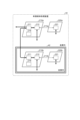
- FIG. 1 is a diagram for explaining an overview of a general-purpose control board according to an embodiment.
- FIG. 2 is a diagram for explaining an example of a valuable medium processing device on which the base substrate shown in FIG. 1 is mounted.
- FIG. 3 is a diagram showing an outline of a mounting form of a general-purpose control board and a base board in a valuable medium processing device.
- FIG. 4 is a diagram showing another example of the configuration of the core module.
- FIG. 5 is a diagram showing an example of the configuration of a program implemented in a core module and an example of the configuration of an FPGA function implementation.
- FIG. 6 is a diagram illustrating an example of the configuration of an extension module.
- FIG. 7 is a diagram showing an example of mounting a base board using only a core module.
- FIG. 8 is a diagram showing an example of implementation of a core module and an extension module.
- FIG. 9 is a diagram showing another implementation example of the core module and the extension module.
- FIG. 10 is a diagram for explaining an outline of an implementation example that ensures security in a valuable medium processing device.
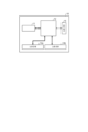
- Fig. 1 is a diagram for explaining the overview of the general-purpose control board according to the present embodiment.
- a core module 10 shown in Fig. 1 is the general-purpose control board according to the present embodiment.
- the general-purpose control board may include an extension module 20.
- the core module 10 has a CPU 11 that controls the entire device in which the general-purpose control board is implemented, and an FPGA 12 that controls multiple sensor circuits 32 and multiple motor circuits 33.
- the expansion module 20 has an FPGA 21 for increasing the number of sensor circuits 32 and motor circuits 33 mounted and expanding the functions.
- the core module 10 and the expansion module 20 are mounted on a base substrate 30 developed for each product.
- the core module 10 and the expansion module 20 are connected via a connection cable 13 or wiring formed on the base substrate 30.
- the core module 10 and the expansion module 20 are connected using a serial I/O interface.
- As the serial I/O interface for example, an unbalanced transmission method such as RS-232C, a differential transmission method such as RS-422 or LVDS (Low Voltage Differential Signaling) is used.
- control signals from the CPU 11 and sensor data from the FPGA 21 are transmitted between the core module 10 and the expansion module 20.
- the CPU 11 and FPGA 12 are connected using the external bus interface of the CPU 11.
- the CPU 11 and FPGA 12 are connected using a parallel I/O interface.
- the FPGA 12 and FPGA 21 are also connected to the external sensor circuit 32 and motor circuit 33 using a parallel I/O interface.
- the base board 30, which is developed for each product, has a core module 10, an expansion module 20, a communication circuit 31, multiple sensor circuits 32, multiple motor circuits 33, and multiple connectors 34a, 34b, 34c, 34d, and 34e (hereinafter, sometimes collectively referred to as "connectors 34").
- the connectors 34 are used to connect to devices such as sensors and motors.
- the communication circuit 31 is a circuit for communicating with a management device that manages the products.
- the sensor circuit 32 is connected to the connector 34 via wiring formed on the base substrate 30.
- the sensor circuit 32 is a circuit for receiving signals from a sensor connected to the connector 34.
- the motor circuit 33 is connected to the connector 34 via wiring formed on the base substrate 30.
- the motor circuit 33 is a circuit for driving a motor connected to the connector 34.
- the core module 10 and the expansion module 20 are mounted on the base substrate 30 using connectors.
- the core module 10 and the expansion module 20 may be surface-mounted on the base substrate 30 by providing surface-mount terminals (e.g., BGA (Ball Grid Array)) on the back of the core module 10 and the expansion module 20.
- surface-mount terminals e.g., BGA (Ball Grid Array)
- the control program of the CPU 11 implemented in the core module 10 includes a program that controls the user interface and the like that is used in common among multiple products, and a program that realizes the cumulative specifications required to control multiple types of products that are assumed in advance. Details of the control program will be described later.
- the FPGA 12 implemented in the core module 10 and the FPGA 21 implemented in the expansion module 20 are implemented with multiple functional logics for controlling the sensor circuits 32 and motor circuits 33 of multiple manufacturers, which are implemented on a base board 30 developed for each device. That is, when a device is developed, a base board 30 is prepared for this device on which a CPU 11 and at least one FPGA 12, 21 are detachably mounted, and the FPGAs 12, 21 are pre-implemented with functional logic corresponding to each of multiple types of external devices such as sensors and motors that may be used with this device.
- the CPU 11 automatically determines which manufacturer's sensor circuit 32 and/or motor circuit 33 has been implemented.
- the CPU 11 notifies the FPGAs 12 and 21 of the determination result, and one of the multiple functional logics implemented in the FPGAs 12 and 21 is selected.
- the determination of which manufacturer's sensor circuit 32 and/or motor circuit 33 is implemented may be performed by implementing functional logic that performs automatic determination in FPGA 12 and FPGA 21 and using that functional logic.
- the general-purpose control board has a core module 10 and an expansion module 20.
- the CPU 11 of the core module 10 can execute a program that controls a user interface and the like that is used in common among a plurality of products, and a program that realizes cumulative specifications necessary for controlling a plurality of products that are assumed in advance.
- the FPGA 12 implemented in the core module 10 and the FPGA 21 implemented in the expansion module 20 are implemented with a plurality of functional logics that control a plurality of types of sensor circuits 32 and motor circuits 33 implemented on a base substrate 30 developed for each device.
- the CPU 11 automatically determines the type of the implemented sensor circuit 32 and/or motor circuit 33, and notifies the FPGA 12 and FPGA 21 of the determination result, so that one of the plurality of functional logics implemented in the FPGA 12 and FPGA 21 is selected. Therefore, by using a general-purpose control board, products can be manufactured efficiently even if the parts implemented on the product-specific printed circuit board are changed to alternative parts. Specifically, even if the type of sensor circuit 32 mounted on the base substrate 30 is changed due to, for example, changing the sensor to an alternative, the core module 10 and extension module 20 that were previously in use can be mounted on the changed base substrate 30 to achieve control of the alternative sensor.
- the general-purpose control board can be used by multiple devices. Therefore, by having a large inventory of general-purpose control boards, the impact on product manufacturing can be reduced even if it becomes difficult to obtain the CPU 11, FPGA 12, and FPGA 21 that are implemented on the general-purpose control board.
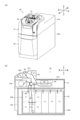
- FIG. 2 is a perspective view of the exterior of the valuable medium processing device 40 on which the base substrate 30 shown in Fig. 1 is mounted, and a schematic diagram of the configuration.
- the directions (front, back, left, right, up, down) used in the following explanation correspond to the directions when the valuable medium processing device 40 installed on a horizontal surface is viewed from the front.
- the front side of the valuable medium processing device 40 is the side where the deposit unit 51 and withdrawal unit 52 are formed.
- the rear side of the valuable medium processing device 40 is the side opposite to the side where the deposit unit 51 and withdrawal unit 52 are formed.
- the valuable medium processing device 40 comprises a processing unit 41 and a safe unit 42.
- the processing unit 41 is provided above the safe unit 42.
- the processing unit 41 has a processing housing 41a and a processing movable part 41b.
- the processing housing 41a is formed in a rectangular box shape that extends in the front-rear direction and opens to the front.
- the processing housing 41a houses the processing movable part 41b.
- the processing movable part 41b can be pulled out to the front from the processing housing 41a.
- the processing movable part 41b has a deposit section 51, a withdrawal section 52, an identification section 53, and a processing side transport section 60.
- the deposit unit 51 is an insertion unit into which banknotes are inserted.
- the deposit unit 51 is provided in front of the processing movable unit 41b.
- the deposit unit 51 has an upwardly opening deposit port 51a.
- An operator manually inserts banknotes into the deposit unit 51 through the deposit port 51a.
- the deposit unit 51 can hold multiple banknotes in a stacked state.
- the deposit unit 51 is provided with a payout mechanism that pays out the banknotes inserted into the deposit unit 51 one by one to the processing side transport unit 60.
- the withdrawal unit 52 is a dispensing unit from which banknotes are dispensed.
- the withdrawal unit 52 is provided in front of the deposit unit 51, in the front part of the movable processing unit 41b.
- the withdrawal unit 52 can hold multiple banknotes in a stacked state. An operator can manually remove banknotes accumulated in the withdrawal unit 52 through the withdrawal port 52a.
- the withdrawal unit 52 may be provided with a shutter for opening and closing the withdrawal port 52a.
- the recognition unit 53 recognizes banknotes.
- the recognition unit 53 is provided in the processing side transport unit 60, and performs recognition processing on banknotes transported by the processing side transport unit 60. In the recognition processing, the recognition unit 53 recognizes the denomination of the banknote.
- the recognition unit 53 may also recognize the fitness, newness, authenticity, transport status, serial number affixed to the banknote, etc.
- the base substrate 30 is used by the recognition unit 53.
- the processing side transport unit 60 transports banknotes within the processing unit 41.
- the processing side transport unit 60 transports the banknotes so that multiple banknotes are consecutively spaced apart in the transport direction.
- the processing side transport unit 60 transports the banknotes so that the edge of the long side of the banknote is at the front in the transport direction.
- the processing side transport unit 60 may also transport the banknotes so that the edge of the short side of the banknote is at the front in the transport direction.
- the processing side transport unit 60 has a transport path.
- the transport path is composed of a transport mechanism for transporting banknotes, such as a transport roller and a transport belt, a guide member for guiding the transported banknotes, and a branching mechanism for switching the transport direction of the banknotes, such as a branching claw.
- the processing side transport unit 60 has a drive mechanism, such as a motor and gears. The drive mechanism drives the transport mechanism and branching mechanism of the transport path.
- the transport path of the processing side transport unit 60 is connected to the deposit unit 51, the withdrawal unit 52, and the safe side transport unit 90, which will be described later.
- the safe section 42 has a safe housing 42a and a safe movable section 42b.
- the safe housing 42a is formed in the shape of a rectangular parallelepiped box extending in the front-rear direction.
- An openable and closable door 130 is provided at the front end of the safe housing 42a.
- the door 130 can be locked.
- the door 130 is provided with an electronic lock.
- the safe housing 42a houses the safe movable section 42b.
- the protection level of the safe housing 42a is higher than the protection level of the processing housing 41a.
- the safe housing 42a is made of a metal plate having a predetermined thickness or more.
- the safe movable section 42b can be pulled out to the front. When the door 130 of the safe housing 42a is opened, the operator can pull the safe movable section 42b out to the front from the safe housing 42a.
- the safe movable section 42b has a plurality of storage devices 71 and a safe-side transport section 90. Each of the plurality of storage devices 71 stores banknotes. Each of the plurality of storage devices 71 dispenses the stored banknotes.
- the safe-side transport unit 90 transports banknotes within the safe unit 42.
- the safe-side transport unit 90 transports the banknotes so that multiple banknotes are consecutively spaced apart in the transport direction.
- the safe-side transport unit 90 transports the banknotes so that the edge of the long side of the banknote is at the front in the transport direction.
- the safe-side transport unit 90 may also transport the banknotes so that the edge of the short side of the banknote is at the front in the transport direction.
- the safe-side transport unit 90 has a transport path.
- the transport path is composed of, for example, a transport mechanism for transporting banknotes, such as a transport roller and a transport belt, a guide member for guiding the transported banknotes, and a branching mechanism for switching the transport direction of the banknotes, such as a branching claw.
- the safe-side transport unit 90 has a drive mechanism, such as a motor and gears. The drive mechanism drives the transport mechanism and branching mechanism of the transport path.
- the transport path of the safe-side transport unit 90 is connected to the processing-side transport unit 60 via a through passage provided in the upper wall of the safe housing 42a.
- the transport path of the safe-side transport unit 90 is connected to multiple storage devices 71.
- the valuable medium processing device 40 having the above-mentioned configuration can perform various banknote processes, including banknote deposit and withdrawal processes, but the content of each banknote process and the operation of each part during each banknote process are well known, so a description will be omitted.
- FIG. 3 is a diagram showing an outline of the implementation form of the general-purpose control board and base board 30 in the valuable medium processing device 40.
- the core module 10 and the expansion module 20 are provided on the base board 30, but as shown in FIG. 3, the core module 10 may be provided away from the base board 30, i.e., separately from the base board 30.
- the valuable medium processing device 40 is equipped with a core module 10, which is a general-purpose control board, a base board 30 developed for each device, and a mechanical mechanism M.
- the core module 10 has a CPU 11, an FPGA 12, and a connector 15 for transmitting serial I/O signals, which are provided on a printed circuit board.
- the CPU 11 and FPGA 12 of the core module 10 are connected using an external bus interface of the CPU 11 via wiring formed on a printed circuit board.
- the external bus interface of the CPU 11 transmits parallel I/O signals.
- the FPGA 12 is connected to the connector 15 via wiring formed on the printed circuit board.
- the FPGA 12 is connected to the connector 15 using a serial I/O interface.
- the core module 10 may be provided with connectors for connecting to the sensor circuit 32 and the motor circuit 33.
- the base substrate 30 has an expansion module 20, a communication circuit 31, a plurality of sensor circuits 32, a plurality of motor circuits 33, and a plurality of connectors 34a, 34b, 35.
- the expansion module 20 and the connector 35 are connected using a serial I/O interface via wiring formed on the base substrate 30.
- the expansion module 20, the communication circuit 31, the plurality of sensor circuits 32, and the plurality of motor circuits 33 are connected using a parallel I/O interface via wiring formed on the base substrate 30.
- the core module 10 and the base substrate 30 are connected using a serial I/O interface via a connector 15, a connection cable 13, and a connector 35.
- the multiple sensor circuits 32 and the connector 34 are connected using a parallel I/O interface via wiring formed on the base substrate 30.
- the sensor circuit 32 is connected to two connectors 34a.
- the multiple motor circuits 33 and the connector 34 are connected using a parallel I/O interface via wiring formed on the base substrate 30.
- the motor circuit 33 is connected to two connectors 34b.
- the mechanical mechanism M includes a plurality of sensors 200 and a plurality of motors 201.
- the plurality of sensors 200 include line sensors, magnetic sensors, image sensors, etc., which acquire data for identifying banknotes in the identification unit 53 of the valuable medium processing device 40.
- the sensor 200 and the connector 34 of the base substrate 30 are connected using a parallel I/O interface via a connection cable 36. In the example shown in FIG. 3, the sensor 200 is connected to the connector 34a.
- the multiple motors 201 include a motor that drives the transport mechanism of the transport paths of the processing side transport section 60 and the safe side transport section 90 of the valuable medium processing device 40, and a motor that drives the branching mechanism.
- the motors 201 and the connector 34 of the base substrate 30 are connected via a connection cable 36. In the example shown in FIG. 3, the motor 201 is connected to the connector 34b.
- FIG. 4 is a diagram showing another example of the configuration of the core module 10.
- the same parts as those in the core module 10 described in FIG. 3 are given the same reference numerals, and detailed descriptions thereof will be omitted.
- the core module 10 shown in FIG. 4 has a CPU 11, an FPGA 12, connectors 14a and 14b (hereinafter, sometimes collectively referred to as "connectors 14"), and a connector 15.
- the core module 10 shown in FIG. 4 is equipped with connectors 14a and 14b that can be directly connected to the sensor circuit 32 and motor circuit 33 provided on the base substrate 30. This makes it possible to connect the sensor circuit 32 and motor circuit 33 to the connector 14 and use the core module 10 alone.
- the FPGA 12 and the connectors 14a and 14b are connected using a parallel I/O interface via wiring formed in the core module 10.
- the FPGA 12 is connected to the connector 15 using a serial I/O interface via wiring formed in the core module 10 in order to connect to the expansion module 20.
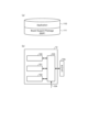
- FIG. 5 is a diagram showing an example of the configuration of a program implemented in the core module 10, and an example of the configuration of the functional implementation of the FPGAs 12 and 21.
- the programs for operating the CPU 11 of the core module 10 include an Application program 110 and a Board Support Package (BSP) program 111.
- the Application program 110 is a program that differs for each product.
- the Application program includes programs related to the user interface of the product.
- the Board Support Package program 111 is a program that is used in common for each product.
- the Board Support Package program 111 includes programs related to processes such as banknote identification processing that is commonly performed by multiple types of valuable medium processing devices 40 and monitoring the transport status of the processing side transport unit 60 and the safe side transport unit 90.
- the FPGA 12 implemented in the core module 10 and the FPGA 21 implemented in the expansion module 20 implement functional logic that controls the sensor circuit 32 and motor circuit 33 implemented on the base substrate 30. Below, the functional logic that controls the motor circuit 33 will be explained as an example.
- the motor 201 used in the mechanical mechanism M will be one of three motors 201 made by companies A, B, and C.
- the functional logic 100 that controls the motor 201 made by company A the functional logic 101 that controls the motor 201 made by company B, and the functional logic 102 that controls the motor 201 made by company C are implemented in advance in the FPGA 12.
- the CPU 11 of the core module 10 determines which company's motor circuit 33, A to C, is implemented on the base substrate 30.
- the CPU 11 sends a selection signal based on the determination result via a selection signal line 104 to a selector 103 implemented on the FPGA 12.
- a selector 103 implemented on the FPGA 12.
- an identification mechanism for identifying which company's motor 201 the motor circuit 33 corresponds to can be implemented on the base substrate 30 so that the CPU 11 can determine which company's motor circuit 33 is implemented.
- a 2-bit DIP (Dual In-line Package) switch is implemented on the base substrate 30, and when the DIP switch is set to "00", it selects a motor circuit from company A, when the DIP switch is set to "01”, it selects a motor circuit from company B, and when the DIP switch is set to "10", it selects a motor circuit from company C.
- the CPU 11 When the CPU 11 is powered on, it reads the setting of this DIP switch and sends a selection signal to a selector 103 implemented in the FPGA 12 via a selection signal line 104. Note that although the use of a DIP switch has been described here, a circuit that sends an identification signal may be implemented in advance in the motor circuit 33.
- the FPGA 12 sends a signal of the functional logic selected by the selector 103 to the connector 14a. For example, when the functional logic 100 is selected by the selector 103, the FPGA 12 sends a control signal corresponding to the functional logic 100 to the connector 14a. Note that the same function is also implemented in the FPGA 21 of the expansion module 20.
- FIG. 6 is a diagram showing an example of the configuration of the expansion module 20.
- the expansion module 20 has an FPGA 21, connectors 22a, 22b, 22c, and 22d (hereinafter sometimes collectively referred to as "connectors 22"), and connectors 23a and 23b.
- the FPGA 21 and the connector 22 are connected using a parallel I/O interface via wiring formed on a printed circuit board.
- the FPGA 21 and the connector 23a for connecting to the core module 10 are connected using a serial I/O interface via wiring formed on the printed circuit board.
- the FPGA 21 and the connector 23b for connecting to another expansion module 20 are connected using a serial I/O interface via wiring formed on the printed circuit board.
- the program for operating the CPU 11 and the functional logic of the FPGA 12 and FPGA 21 can be modified from an external device, and access control related to the modifications can also be executed.
- the program for operating the CPU 11 of the core module 10 is access-controlled so that it can be modified only from a first management device used by the manufacturer of the valuable medium processing device 40.
- the functional logic of the FPGA 12 implemented in the core module 10 and the FPGA 21 implemented in the expansion module 20 may be access-controlled so that it can be modified not only from the first management device used by the manufacturer, but also from a second management device used by a company other than the manufacturer.
- access control may be performed based on the IP addresses and/or MAC addresses of the first management device and the second management device.
- FIG. 3 an example is shown in which both the core module 10 and the extension module 20 are used, but only the core module 10 may also be used.
- a valuable medium processing device 40 that uses only the core module 10 is described. Note that parts that are the same as those in the implementation form of the valuable medium processing device 40 shown in FIG. 3 are given the same reference numerals, and detailed descriptions thereof will be omitted.
- FIG. 7 is a diagram showing an implementation form of a base substrate 30 that uses only the core module 10.
- the mechanical mechanism M of the valuable medium processing device 40 shown in FIG. 7 has a base substrate 30 on which a core module 10 is mounted, a plurality of sensors 200, and a plurality of motors 201.
- the base substrate 30 does not include an expansion module 20, and only the core module 10 is mounted thereon.
- the core module 10 is mounted on the base substrate 30 using connectors 14a, 14b, and 15.
- the FPGA 12, the communication circuit 31, the multiple sensor circuits 32, and the multiple motor circuits 33 are connected using a parallel I/O interface via connectors 14a and 14b and wiring formed on the base substrate 30.
- the signal from the sensor 200 is transmitted to the CPU 11 of the core module 10 via the connection cable 36, the connector 34a, the sensor circuit 32, the connector 14a or the connector 14b, and the FPGA 12.
- the CPU 11 uses the transmitted signal to execute the bill recognition process.
- the CPU 11 also controls the motor 201 via the FPGA 12, the connector 14a or the connector 14b, the motor circuit 33, the connector 34b, and the connection cable 36.
- FIG. 8 is a diagram showing the mounting form of the core module 10 and the expansion module 20.
- the valuable medium processing device 40 shown in FIG. 8 has three mechanical mechanisms M1 to M3.
- the first mechanical mechanism M1 has a base substrate 30a on which the core module 10 and the expansion module 20 are mounted, a plurality of sensors 200, and a plurality of motors 201.
- the second mechanical mechanism M2 and the third mechanical mechanism M3 each have a plurality of sensors 200 and a plurality of motors 201.
- the base substrate 30a has a core module 10, an expansion module 20, a communication circuit 31, a plurality of sensor circuits 32, a plurality of motor circuits 33, and connectors 34c, 34d, 34e, 34f, 34g, and 34h.
- the core module 10 and the expansion module 20 are connected using a serial I/O interface via the connector 15, the connector 23a, and wiring formed on the base substrate 30a.
- the core module 10 and some of the multiple sensor circuits 32 are connected using a parallel I/O interface via the connector 14 and wiring formed on the base substrate 30a.
- the core module 10 and some of the multiple motor circuits 33 are connected using a parallel I/O interface via the connector 14 and wiring formed on the base substrate 30a.
- the expansion module 20 and some of the multiple sensor circuits 32 are connected using a parallel I/O interface via the connector 22 and wiring formed on the base substrate 30a.
- the expansion module 20 and some of the multiple motor circuits 33 are connected using a parallel I/O interface via the connector 22bb and wiring formed on the base substrate 30a.
- the multiple sensor circuits 32 are connected to connectors 34c, 34e, or 34g using a parallel I/O interface according to the corresponding sensors 200.
- the multiple motor circuits 33 are connected to connectors 34d, 34f, or 34h using a parallel I/O interface according to the corresponding motors 201.
- the base substrate 30a and the multiple sensors 200 are connected using a parallel I/O interface via the connector 34c and the connection cable 36.
- the base substrate 30a and the multiple motors 201 are connected using a parallel I/O interface via the connector 34d and the connection cable 36.
- the base substrate 30a and the multiple sensors 200 of the second mechanical mechanism M2 are connected using a parallel I/O interface via the connector 34e and the connection cable 36.
- the base substrate 30a and the multiple motors 201 of the second mechanical mechanism M2 are connected using a serial I/O interface via the connector 34f and the connection cable 36.
- the base substrate 30a and the multiple sensors 200 of the third mechanical mechanism M3 are connected using a parallel I/O interface via connector 34g and connection cable 36.
- the base substrate 30a and the multiple motors 201 of the third mechanical mechanism M3 are connected using a parallel I/O interface via connector 34h and connection cable 36.
- signals from the multiple sensors 200 of the first mechanical mechanism M1 are transmitted to the CPU 11 via the connection cable 36, the connector 34c, the sensor circuit 32, the connector 14, and the FPGA 12.
- Signals from the multiple sensors 200 of the second mechanical mechanism M2 are transmitted to the CPU 11 via the connection cable 36, connector 34e, sensor circuit 32, connector 14, and FPGA 12.
- Signals from the multiple sensors 200 of the third mechanical mechanism M3 are transmitted to the CPU 11 via the connection cable 36, connector 34g, sensor circuit 32, connector 22, FPGA 21, connector 23a, connector 15, and FPGA 12. This allows the CPU 11 of the core module 10 to perform banknote recognition processing.
- Control signals to the multiple motors 201 of the first mechanical mechanism M1 are transmitted from the CPU 11 to the motors 201 via the FPGA 12, connector 14, motor circuit 33, connector 34d, and connection cable 36.
- Control signals to the multiple motors 201 of the second mechanical mechanism M2 are transmitted to the motors 201 from the CPU 11 via the FPGA 12, connector 14, motor circuit 33, connector 34f, and connection cable 36.
- Control signals to the multiple motors 201 of the third mechanical mechanism M3 are transmitted to the motors 201 from the CPU 11 via the FPGA 12, connector 15, connector 23a, FPGA 21, connector 22, motor circuit 33, connector 34h, and connection cable 36. This allows the CPU 11 of the core module 10 to control each of the multiple motors 201 of the first mechanical mechanism M1, the second mechanical mechanism M2, and the third mechanical mechanism M3.
- FIG. 9 is a diagram showing another implementation form of a core module 10 and an expansion module 20.
- the valuable medium processing device 40 shown in FIG. 9 has four mechanical mechanisms M11 to M14.
- the first mechanical mechanism M11 has a base substrate 30c on which the core module 10 is mounted, a plurality of sensors 200, and a plurality of motors 201.
- the second mechanical mechanism M12 has a base substrate 30d on which the first expansion module 20a and the second expansion module 20b are mounted, a plurality of sensors 200, and a plurality of motors 201.
- the third mechanical mechanism M13 has a plurality of sensors 200 and a plurality of motors 201.
- the fourth mechanical mechanism M14 has a plurality of sensors 200 and a plurality of motors 201.
- the base substrate 30c of the first mechanical mechanism M11 has a configuration in which a connector 35a is added to the base substrate 30 described in FIG. 7 in order to transmit control signals from the CPU 11 to another base substrate.
- the core module 10 and the connector 35a are connected using a serial I/O interface via the connector 15 and wiring formed on the base substrate 30c.
- the base substrate 30c and the base substrate 30d are connected using a serial I/O interface via the connector 35a mounted on the base substrate 30c and the connector 35b mounted on the base substrate 30d. This enables mutual transmission of control signals transmitted from the CPU 11 and acquired data from the multiple sensors 200 transmitted to the CPU 11 between the base substrate 30c and the base substrate 30d.
- the base substrate 30d of the second mechanical mechanism M12 has a first expansion module 20a, a second expansion module 20b, a communication circuit 31, a number of sensor circuits 32, a number of motor circuits 33, connectors 34c, 34d, 34e, 34f, 34g, 34h, and a connector 35b.
- the first expansion module 20a is mounted on the base substrate 30d using a plurality of connectors 22, connector 23a, and connector 23b.
- the first expansion module 20a and connector 35b are connected using a serial I/O interface via the connector 23a and wiring formed on the base substrate 30d.
- the first expansion module 20a and the second expansion module 20 are connected using a serial I/O interface via the connector 23b, wiring formed on the base substrate 30d, and connector 23c.
- the first expansion module 20a and some of the multiple sensor circuits 32 are connected using a parallel I/O interface via the connector 22 and wiring formed on the base substrate 30d.
- the first expansion module 20a and some of the multiple motor circuits 33 are connected using a parallel I/O interface via the connector 22 and wiring formed on the base substrate 30d.
- the second expansion module 20b and some of the multiple sensor circuits 32 are connected using a parallel I/O interface via the connector 22 and wiring formed on the base substrate 30d.
- the second expansion module 20b and some of the multiple motor circuits 33 are connected using a parallel I/O interface via the connector 22 and wiring formed on the base substrate 30d.
- the multiple sensor circuits 32 are connected to connectors 34c, 34e, or 34g using a parallel I/O interface according to the corresponding sensors 200.
- the multiple motor circuits 33 are connected to connectors 34d, 34f, or 34h using a parallel I/O interface according to the corresponding motors 201.
- the base substrate 30d and the multiple sensors 200 are connected using a parallel I/O interface via the connector 34c and the connection cable 36.
- the base substrate 30a and the multiple motors 201 are connected using a parallel I/O interface via the connector 34d and the connection cable 36.
- the base substrate 30d and the multiple sensors 200 of the third mechanical mechanism M13 are connected using a parallel I/O interface via the connector 34e and the connection cable 36.
- the base substrate 30d and the multiple motors 201 of the third mechanical mechanism M13 are connected using a parallel I/O interface via the connector 34f and the connection cable 36.
- the base substrate 30d and the multiple sensors 200 of the fourth mechanical mechanism M14 are connected using a parallel I/O interface via the connector 34g and the connection cable 36.
- the base substrate 30d and the multiple motors 201 of the fourth mechanical mechanism M14 are connected using a parallel I/O interface via the connector 34h and the connection cable 36.
- a serial I/O interface is used to connect between the sensors 200 and the multiple base substrates connected to them.
- the expansion module 20 By transmitting and receiving signals from the serial I/O interface via the expansion module 20, it becomes possible to transmit acquired data from the multiple sensors 200 connected to each base substrate to the CPU 11 of the core module 10. This allows the CPU 11 of the core module 10 to perform banknote recognition processing.
- a serial I/O interface is used to connect between the motors 201 and the multiple base boards connected to them.
- the expansion module 20 By sending and receiving signals of the serial I/O interface via the expansion module 20, it becomes possible to transmit control signals from the CPU 11 of the core module 10 to the multiple motors 201 connected to each base board. This allows the CPU 11 of the core module 10 to control the multiple motors 201 of the first mechanical mechanism M11, the second mechanical mechanism M12, the third mechanical mechanism M13, and the fourth mechanical mechanism M14.
- Figure 9 illustrates an example in which two base substrates are connected, three or more base substrates may be connected by mounting one or more expansion modules 20 and connectors on each base substrate and connecting them via a serial I/O interface.
- encrypted communication may be performed at the bus interface between the CPU 11 and FPGA 12 of the core module 10, and at the serial I/O interface between the core module 10 and the expansion module 20.
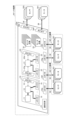
- FIG. 10 is a diagram for explaining an outline of an implementation form that ensures security in the valuable medium processing device 40. Note that FIG. 10 illustrates only a portion of the valuable medium processing device 40, and omits the illustration of the base board, showing only the core modules 210a, 210b and the extension modules 220a, 220b.
- the core module 210a has a CPU 211, an FPGA 212, and a TPM (Trusted Platform Module) 216.
- the CPU 211 controls the entire valuable medium processing device 40 on which the base substrate is mounted.
- the FPGA 212 is implemented with functional logic that controls multiple sensor circuits 32 and multiple motor circuits 33 used in the valuable medium processing device 40.
- the FPGA 212 is implemented with an encryption IP (Intellectual Property) core to encrypt the serial I/O interface.
- the type of encryption IP core is not particularly limited. For example, an IP core such as an AES (Advanced Encryption Standard) method or a SHA2 (Secure Hash Algorithm 2) method may be used.
- TPM216 generates and stores private keys and other data used to encrypt communications with a second management device other than the manufacturer.
- the core module 210a transmits and receives encrypted data using the TPM 216 via the system bus between the CPU 211 and FPGA 212. Between the core module 210a and the expansion module 220a, data is transmitted and received using encryption IP cores implemented in the FPGA 212 and FPGA 221. Similarly, data is transmitted and received between the core module 210b and the expansion module 220b using encryption IP cores.
- the interface between the core module 210a implemented inside the processing unit 41 of the valuable medium processing device 40 and the core module 210b implemented inside the safe unit 42 also transmits and receives data encrypted using a private key generated based on the TPM 216.
- the core module 210a may communicate with an external device, for example, a second management device other than the manufacturer of the valuable medium processing device 40, and even in such external communications, data encrypted using a private key generated based on the functions of the TPM 216 is transmitted and received.
- the TPM 216 is implemented in the core module 210a, and the private key etc. used for encryption is generated and stored by the TPM 216, and the private key is used to encrypt communication between the CPU 211 of the core module 210a and the CPU 211 of the core module 210b.
- an encryption IP core is implemented in the FPGA 212 implemented in the core module 210a and the FPGA 221 implemented in the expansion module 220a, and communication between the FPGA 212 and the FPGA 221 is encrypted. This makes it possible to strengthen security so that communication between modules and between the modules and external devices is not eavesdropped on.
- each of the FPGAs 21 from companies A, B, and C is implemented with multiple functional logics that control sensor circuits 32 and motor circuits 33 from multiple manufacturers that are implemented on a base substrate 30 developed for each device.
- the multiple functional logics implemented in the FPGA can be designed as a common program by using RTL (Register Transfer Level) design, which allows common design regardless of the FPGA manufacturer.
- the CPU 11 of the core module 10 is also equipped with a program that operates any of the FPGAs 21 made by companies A, B, and C, and is configured to determine which company's FPGA has been implemented and select the corresponding program to operate. In this way, even if it becomes difficult to obtain FPGAs made by company A, product manufacturing can continue by implementing FPGAs made by companies B and C in the expansion module 20.
- the FPGA 12 mounted on the core module 10 can be any FPGA from multiple pre-designated manufacturers. In this way, even if it becomes difficult to obtain FPGAs from company A, product manufacturing can continue by mounting FPGAs from companies B and C on the core module 10.
Landscapes
- Engineering & Computer Science (AREA)
- Computer Hardware Design (AREA)
- Theoretical Computer Science (AREA)
- General Engineering & Computer Science (AREA)
- Physics & Mathematics (AREA)
- General Physics & Mathematics (AREA)
- Computing Systems (AREA)
- Manufacturing & Machinery (AREA)
- Microelectronics & Electronic Packaging (AREA)
- Pinball Game Machines (AREA)
- Microcomputers (AREA)
Abstract
Description
本実施形態に係る汎用制御基板の概要について説明する。図1は、本実施形態に係る汎用制御基板の概要を説明するための図である。図1に示すコアモジュール10が本実施形態で言う汎用制御基板である。汎用制御基板に、拡張モジュール20が含まれていてもよい。
ベース基板30が実装される装置の一例として、有価媒体処理装置40の概要について説明する。図2は、図1に示したベース基板30が実装される有価媒体処理装置40の外観の斜視図及び構成の概略図である。
Claims (9)
- 第1の装置に組み込まれる第1の固有基板及び第2の装置に組み込まれる第2の固有基板のいずれにも実装可能な汎用制御基板であって、
装置のユーザインターフェースの制御及び前記装置の機能を実現する第1のアプリケーションを実行して前記装置を制御するプロセッサと、
前記プロセッサが実行する前記第1のアプリケーションに基づいて前記固有基板を動作させる第2のアプリケーションを実装するプログラマブル素子と
を備えることを特徴とする汎用制御基板。 - 前記プロセッサ及び第1の前記プログラマブル素子を含む第1の基板と、
第1の前記プログラマブル素子と接続される第2の前記プログラマブル素子を含む第2の基板と
を備えることを特徴とする請求項1に記載の汎用制御基板。 - 前記第1の基板と、前記第2の基板とは、シリアルI/Oインターフェースを用いて接続される
ことを特徴とする請求項2に記載の汎用制御基板。 - 前記第1の基板と、前記第2の基板とがデータを暗号化して通信を行うことを特徴とした請求項3に記載の汎用制御基板。
- 前記第1のアプリケーションは、第1の制御装置からのみ変更可能であり、
前記第2のアプリケーションは、前記第1の制御装置及び第2の制御装置から変更可能である
ことを特徴とした請求項1に記載の汎用制御基板。 - 前記装置は、有価媒体の処理を行う有価媒体処理装置であることを特徴とする請求項1~4のいずれか1項に記載の汎用制御基板。
- 前記有価媒体処理装置は、有価媒体の処理に供する複数のセンサ及び/又は複数のモータを含み、
前記複数のセンサ及び/又は前記複数のモータが前記プログラマブル素子と電気的に接続される
ことを特徴とする請求項6に記載の汎用制御基板。 - 前記複数のセンサ及び/又は前記複数のモータは、前記プログラマブル素子を介して前記プロセッサに電気的に接続される
ことを特徴とする請求項6に記載の汎用制御基板。 - 前記有価媒体処理装置は、金庫をさらに備え、
前記汎用制御基板を実装した前記固有基板が前記金庫内に収められている
ことを特徴とする請求項6に記載の汎用制御基板。
Priority Applications (2)
| Application Number | Priority Date | Filing Date | Title |
|---|---|---|---|
| EP24823205.0A EP4730146A1 (en) | 2023-06-16 | 2024-05-24 | General-purpose control board |
| US19/398,053 US20260079878A1 (en) | 2023-06-16 | 2025-11-24 | General-purpose control board |
Applications Claiming Priority (2)
| Application Number | Priority Date | Filing Date | Title |
|---|---|---|---|
| JP2023-099242 | 2023-06-16 | ||
| JP2023099242A JP2024179910A (ja) | 2023-06-16 | 2023-06-16 | 汎用制御基板 |
Related Child Applications (1)
| Application Number | Title | Priority Date | Filing Date |
|---|---|---|---|
| US19/398,053 Continuation US20260079878A1 (en) | 2023-06-16 | 2025-11-24 | General-purpose control board |
Publications (1)
| Publication Number | Publication Date |
|---|---|
| WO2024257584A1 true WO2024257584A1 (ja) | 2024-12-19 |
Family
ID=93851735
Family Applications (1)
| Application Number | Title | Priority Date | Filing Date |
|---|---|---|---|
| PCT/JP2024/019225 Ceased WO2024257584A1 (ja) | 2023-06-16 | 2024-05-24 | 汎用制御基板 |
Country Status (4)
| Country | Link |
|---|---|
| US (1) | US20260079878A1 (ja) |
| EP (1) | EP4730146A1 (ja) |
| JP (1) | JP2024179910A (ja) |
| WO (1) | WO2024257584A1 (ja) |
Citations (3)
| Publication number | Priority date | Publication date | Assignee | Title |
|---|---|---|---|---|
| JP4717554B2 (ja) | 2005-08-30 | 2011-07-06 | 東芝三菱電機産業システム株式会社 | 製造中止部品対応用変換アダプタ |
| CN205692166U (zh) * | 2016-06-12 | 2016-11-16 | 成都傅立叶电子科技有限公司 | 基于PowerPC架构中央处理器的核心板 |
| CN205692167U (zh) * | 2016-06-12 | 2016-11-16 | 成都傅立叶电子科技有限公司 | 基于PowerPC架构中央处理器的通用核心板 |
-
2023
- 2023-06-16 JP JP2023099242A patent/JP2024179910A/ja active Pending
-
2024
- 2024-05-24 WO PCT/JP2024/019225 patent/WO2024257584A1/ja not_active Ceased
- 2024-05-24 EP EP24823205.0A patent/EP4730146A1/en active Pending
-
2025
- 2025-11-24 US US19/398,053 patent/US20260079878A1/en active Pending
Patent Citations (3)
| Publication number | Priority date | Publication date | Assignee | Title |
|---|---|---|---|---|
| JP4717554B2 (ja) | 2005-08-30 | 2011-07-06 | 東芝三菱電機産業システム株式会社 | 製造中止部品対応用変換アダプタ |
| CN205692166U (zh) * | 2016-06-12 | 2016-11-16 | 成都傅立叶电子科技有限公司 | 基于PowerPC架构中央处理器的核心板 |
| CN205692167U (zh) * | 2016-06-12 | 2016-11-16 | 成都傅立叶电子科技有限公司 | 基于PowerPC架构中央处理器的通用核心板 |
Also Published As
| Publication number | Publication date |
|---|---|
| US20260079878A1 (en) | 2026-03-19 |
| EP4730146A1 (en) | 2026-04-22 |
| JP2024179910A (ja) | 2024-12-26 |
Similar Documents
| Publication | Publication Date | Title |
|---|---|---|
| AU2003204746B2 (en) | Bill Acceptor | |
| CN100392527C (zh) | 盒体、识别信息附件和成像装置 | |
| US6817890B1 (en) | System and method for providing indicators within a connector assembly | |
| US6556450B1 (en) | Methods and apparatus of docking a gaming control board to an interface board in a gaming machine | |
| US9379464B2 (en) | Device for handling value documents | |
| JP2024179910A (ja) | 汎用制御基板 | |
| US9861002B1 (en) | Single channel I/O in a modular sub-chassis | |
| CN201349392Y (zh) | 屏蔽装置及应用所述屏蔽装置的通信设备 | |
| AU2003203217B2 (en) | System and Method for Combining Low-power Signals and High-power Signals on a Single Circuit Board in a Gaming Machine | |
| WO2008135465A2 (en) | Modular connector comprising an ethernet-wlan bridge | |
| JP2002177481A (ja) | パチンコ遊技機の電源基板配設構造 | |
| CN109792412A (zh) | 被配置为使用光学接口或电气接口的网络交换机 | |
| CN113918491A (zh) | 母板 | |
| CN113918495A (zh) | 电源子板 | |
| JP2009195624A (ja) | 遊技機用制御基板アセンブリ | |
| CN101430754B (zh) | 可移动记忆卡桥 | |
| JP4303517B2 (ja) | 遊技機 | |
| US8514437B2 (en) | Image forming apparatus and control method thereof | |
| KR20080062610A (ko) | 통합된 통합된 유에스비 드라이버가 장착된 금융자동화기기 | |
| KR200290664Y1 (ko) | 무인정보단말기의 무선포선장치 | |
| CN114064538A (zh) | 开发平台 | |
| CN114036093A (zh) | 转接子板 | |
| CN114036094A (zh) | 子板 | |
| CN113918493A (zh) | 开发平台 | |
| JP6927075B2 (ja) | 紙幣処理ユニット、紙幣処理方法、及び紙幣処理プログラム |
Legal Events
| Date | Code | Title | Description |
|---|---|---|---|
| 121 | Ep: the epo has been informed by wipo that ep was designated in this application |
Ref document number: 24823205 Country of ref document: EP Kind code of ref document: A1 |
|
| WWE | Wipo information: entry into national phase |
Ref document number: 2024823205 Country of ref document: EP |
|
| NENP | Non-entry into the national phase |
Ref country code: DE |
|
| ENP | Entry into the national phase |
Ref document number: 2024823205 Country of ref document: EP Effective date: 20260116 |
|
| ENP | Entry into the national phase |
Ref document number: 2024823205 Country of ref document: EP Effective date: 20260116 |
|
| ENP | Entry into the national phase |
Ref document number: 2024823205 Country of ref document: EP Effective date: 20260116 |
|
| ENP | Entry into the national phase |
Ref document number: 2024823205 Country of ref document: EP Effective date: 20260116 |
|
| WWP | Wipo information: published in national office |
Ref document number: 2024823205 Country of ref document: EP |