WO2024257580A1 - 炭化珪素エピタキシャル基板、炭化珪素半導体装置の製造方法および炭化珪素エピタキシャル基板の製造方法 - Google Patents
炭化珪素エピタキシャル基板、炭化珪素半導体装置の製造方法および炭化珪素エピタキシャル基板の製造方法 Download PDFInfo
- Publication number
- WO2024257580A1 WO2024257580A1 PCT/JP2024/019082 JP2024019082W WO2024257580A1 WO 2024257580 A1 WO2024257580 A1 WO 2024257580A1 JP 2024019082 W JP2024019082 W JP 2024019082W WO 2024257580 A1 WO2024257580 A1 WO 2024257580A1
- Authority
- WO
- WIPO (PCT)
- Prior art keywords
- silicon carbide
- carbide epitaxial
- substrate
- epitaxial layer
- main surface
- Prior art date
- Legal status (The legal status is an assumption and is not a legal conclusion. Google has not performed a legal analysis and makes no representation as to the accuracy of the status listed.)
- Ceased
Links
Images






Classifications
-
- C—CHEMISTRY; METALLURGY
- C23—COATING METALLIC MATERIAL; COATING MATERIAL WITH METALLIC MATERIAL; CHEMICAL SURFACE TREATMENT; DIFFUSION TREATMENT OF METALLIC MATERIAL; COATING BY VACUUM EVAPORATION, BY SPUTTERING, BY ION IMPLANTATION OR BY CHEMICAL VAPOUR DEPOSITION, IN GENERAL; INHIBITING CORROSION OF METALLIC MATERIAL OR INCRUSTATION IN GENERAL
- C23C—COATING METALLIC MATERIAL; COATING MATERIAL WITH METALLIC MATERIAL; SURFACE TREATMENT OF METALLIC MATERIAL BY DIFFUSION INTO THE SURFACE, BY CHEMICAL CONVERSION OR SUBSTITUTION; COATING BY VACUUM EVAPORATION, BY SPUTTERING, BY ION IMPLANTATION OR BY CHEMICAL VAPOUR DEPOSITION, IN GENERAL
- C23C16/00—Chemical coating by decomposition of gaseous compounds, without leaving reaction products of surface material in the coating, i.e. chemical vapour deposition [CVD] processes
- C23C16/22—Chemical coating by decomposition of gaseous compounds, without leaving reaction products of surface material in the coating, i.e. chemical vapour deposition [CVD] processes characterised by the deposition of inorganic material, other than metallic material
- C23C16/30—Deposition of compounds, mixtures or solid solutions, e.g. borides, carbides, nitrides
- C23C16/42—Silicides
-
- C—CHEMISTRY; METALLURGY
- C23—COATING METALLIC MATERIAL; COATING MATERIAL WITH METALLIC MATERIAL; CHEMICAL SURFACE TREATMENT; DIFFUSION TREATMENT OF METALLIC MATERIAL; COATING BY VACUUM EVAPORATION, BY SPUTTERING, BY ION IMPLANTATION OR BY CHEMICAL VAPOUR DEPOSITION, IN GENERAL; INHIBITING CORROSION OF METALLIC MATERIAL OR INCRUSTATION IN GENERAL
- C23C—COATING METALLIC MATERIAL; COATING MATERIAL WITH METALLIC MATERIAL; SURFACE TREATMENT OF METALLIC MATERIAL BY DIFFUSION INTO THE SURFACE, BY CHEMICAL CONVERSION OR SUBSTITUTION; COATING BY VACUUM EVAPORATION, BY SPUTTERING, BY ION IMPLANTATION OR BY CHEMICAL VAPOUR DEPOSITION, IN GENERAL
- C23C16/00—Chemical coating by decomposition of gaseous compounds, without leaving reaction products of surface material in the coating, i.e. chemical vapour deposition [CVD] processes
- C23C16/44—Chemical coating by decomposition of gaseous compounds, without leaving reaction products of surface material in the coating, i.e. chemical vapour deposition [CVD] processes characterised by the method of coating
- C23C16/458—Chemical coating by decomposition of gaseous compounds, without leaving reaction products of surface material in the coating, i.e. chemical vapour deposition [CVD] processes characterised by the method of coating characterised by the method used for supporting substrates in the reaction chamber
-
- C—CHEMISTRY; METALLURGY
- C30—CRYSTAL GROWTH
- C30B—SINGLE-CRYSTAL GROWTH; UNIDIRECTIONAL SOLIDIFICATION OF EUTECTIC MATERIAL OR UNIDIRECTIONAL DEMIXING OF EUTECTOID MATERIAL; REFINING BY ZONE-MELTING OF MATERIAL; PRODUCTION OF A HOMOGENEOUS POLYCRYSTALLINE MATERIAL WITH DEFINED STRUCTURE; SINGLE CRYSTALS OR HOMOGENEOUS POLYCRYSTALLINE MATERIAL WITH DEFINED STRUCTURE; AFTER-TREATMENT OF SINGLE CRYSTALS OR A HOMOGENEOUS POLYCRYSTALLINE MATERIAL WITH DEFINED STRUCTURE; APPARATUS THEREFOR
- C30B25/00—Single-crystal growth by chemical reaction of reactive gases, e.g. chemical vapour-deposition growth
- C30B25/02—Epitaxial-layer growth
- C30B25/12—Substrate holders or susceptors
-
- C—CHEMISTRY; METALLURGY
- C30—CRYSTAL GROWTH
- C30B—SINGLE-CRYSTAL GROWTH; UNIDIRECTIONAL SOLIDIFICATION OF EUTECTIC MATERIAL OR UNIDIRECTIONAL DEMIXING OF EUTECTOID MATERIAL; REFINING BY ZONE-MELTING OF MATERIAL; PRODUCTION OF A HOMOGENEOUS POLYCRYSTALLINE MATERIAL WITH DEFINED STRUCTURE; SINGLE CRYSTALS OR HOMOGENEOUS POLYCRYSTALLINE MATERIAL WITH DEFINED STRUCTURE; AFTER-TREATMENT OF SINGLE CRYSTALS OR A HOMOGENEOUS POLYCRYSTALLINE MATERIAL WITH DEFINED STRUCTURE; APPARATUS THEREFOR
- C30B29/00—Single crystals or homogeneous polycrystalline material with defined structure characterised by the material or by their shape
- C30B29/10—Inorganic compounds or compositions
- C30B29/36—Carbides
-
- H—ELECTRICITY
- H10—SEMICONDUCTOR DEVICES; ELECTRIC SOLID-STATE DEVICES NOT OTHERWISE PROVIDED FOR
- H10P—GENERIC PROCESSES OR APPARATUS FOR THE MANUFACTURE OR TREATMENT OF DEVICES COVERED BY CLASS H10
- H10P14/00—Formation of materials, e.g. in the shape of layers or pillars
- H10P14/20—Formation of materials, e.g. in the shape of layers or pillars of semiconductor materials
- H10P14/29—Formation of materials, e.g. in the shape of layers or pillars of semiconductor materials characterised by the substrates
Definitions
- This disclosure relates to a silicon carbide epitaxial substrate, a method for manufacturing a silicon carbide semiconductor device, and a method for manufacturing a silicon carbide epitaxial substrate.
- Patent Document 1 JP 2016-149496 A discloses a susceptor on which a coating layer made of diamond is formed.
- a silicon carbide epitaxial substrate includes a silicon carbide substrate, a first silicon carbide epitaxial layer, and a second silicon carbide epitaxial layer.
- the silicon carbide substrate has a first main surface and a second main surface opposite to the first main surface.
- the first silicon carbide epitaxial layer contacts the silicon carbide substrate at the first main surface.
- the second silicon carbide epitaxial layer contacts the silicon carbide substrate at the second main surface.
- the thickness of the first silicon carbide epitaxial layer is greater than the thickness of the second silicon carbide epitaxial layer.
- the areal density of recesses in a central square region of the second silicon carbide epitaxial layer is 5 mm -2 or less.
- the length of one side of the central square region is 5 mm.
- the maximum width of the recesses is 10 ⁇ m or more and 100 ⁇ m or less.
- FIG. 1 is a schematic plan view showing the configuration of a surface of a silicon carbide epitaxial substrate according to this embodiment.
- FIG. 2 is a schematic cross-sectional view taken along line II-II in FIG.
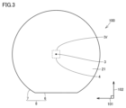
- FIG. 3 is a plan view illustrating the configuration of the back surface of the silicon carbide epitaxial substrate according to this embodiment.
- FIG. 4 is an enlarged view of region IV of FIG.
- FIG. 5 is a schematic cross-sectional view taken along line VV in FIG.
- FIG. 6 is a partial schematic cross-sectional view showing the configuration of an apparatus for manufacturing a silicon carbide epitaxial substrate.
- FIG. 7 is a flow chart that outlines the method for manufacturing a silicon carbide epitaxial substrate according to this embodiment.
- FIG. 8 is a schematic cross-sectional view showing the configuration of a susceptor.
- FIG. 9 is a schematic cross-sectional view showing a step of forming a silicon carbide coating layer on a susceptor.
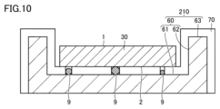
- FIG. 10 is a schematic cross-sectional view showing a step of placing the silicon carbide substrate on a susceptor.
- FIG. 11 is a schematic cross-sectional view showing a step of forming a silicon carbide epitaxial layer on a silicon carbide substrate.
- FIG. 12 is a flowchart that roughly illustrates the method for manufacturing a silicon carbide semiconductor device according to this embodiment.
- FIG. 13 is a schematic cross-sectional view showing a step of preparing a silicon carbide epitaxial substrate.
- FIG. 14 is a schematic cross-sectional view showing a step of forming a body region.
- FIG. 15 is a schematic cross-sectional view showing a step of forming a source region.
- FIG. 16 is a schematic cross-sectional view showing a step of forming a trench in the third main surface of the first silicon carbide epitaxial layer.
- FIG. 17 is a schematic cross-sectional view showing a step of forming a gate insulating film.
- FIG. 18 is a schematic cross-sectional view showing a step of forming a gate electrode and an interlayer insulating film.
- FIG. 19 is a schematic cross-sectional view showing the configuration of a silicon carbide semiconductor device according to this embodiment.
- An object of the present disclosure is to provide a silicon carbide epitaxial substrate capable of improving the yield of silicon carbide semiconductor devices, a method for manufacturing a silicon carbide semiconductor device, and a method for manufacturing a silicon carbide epitaxial substrate.
- An object of the present disclosure is to provide a silicon carbide epitaxial substrate capable of improving the yield of silicon carbide semiconductor devices, a method for manufacturing a silicon carbide semiconductor device, and a method for manufacturing a silicon carbide epitaxial substrate.
- a silicon carbide epitaxial substrate 100 includes a silicon carbide substrate 30, a first silicon carbide epitaxial layer 10, and a second silicon carbide epitaxial layer 20.
- the silicon carbide substrate 30 has a first main surface 1 and a second main surface 2 opposite to the first main surface 1.
- the first silicon carbide epitaxial layer 10 contacts the silicon carbide substrate 30 at the first main surface 1.
- the second silicon carbide epitaxial layer 20 contacts the silicon carbide substrate 30 at the second main surface 2.
- the thickness of the first silicon carbide epitaxial layer 10 is greater than the thickness of the second silicon carbide epitaxial layer 20.
- the areal density of the recesses 5 in a central square region 4 of the second silicon carbide epitaxial layer 20 is 5 mm -2 or less.
- the length of one side of the central square region 4 is 5 mm.
- the maximum width of the recess 5 is 10 ⁇ m or more and 100 ⁇ m or less.
- the outer shape of the recess 5 may have an arc-shaped portion in a plan view.
- the areal density of recesses 5 in the central square region may be equal to or less than 4 mm ⁇ 2 .
- the thickness of the second silicon carbide epitaxial layer 20 may be 0.1 ⁇ m or more and 5 ⁇ m or less.
- the method for manufacturing a silicon carbide semiconductor device includes the following steps: A silicon carbide epitaxial substrate 100 described in any one of (1) to (4) above is prepared. An electrode is formed on the first silicon carbide epitaxial layer 10.
- the method for manufacturing a silicon carbide epitaxial substrate 100 includes the following steps: A silicon carbide coating layer 70 is formed on the susceptor 210 without the silicon carbide substrate 30 being placed. The silicon carbide substrate 30 is placed on the susceptor 210 so that the silicon carbide substrate 30 is in contact with the silicon carbide coating layer 70. A silicon carbide epitaxial layer 40 is formed on the silicon carbide substrate 30.
- silicon carbide particles 9 may be present on the susceptor 210.
- the thickness of the silicon carbide coating layer 70 may be greater than the height of the silicon carbide particles 9.
- FIG. 1 is a plan view schematic diagram showing the configuration of the surface of the silicon carbide epitaxial substrate according to this embodiment.
- FIG. 2 is a cross-sectional schematic diagram along the II-II line in FIG. 1.
- the silicon carbide epitaxial substrate 100 according to this embodiment has a silicon carbide substrate 30, a first silicon carbide epitaxial layer 10, and a second silicon carbide epitaxial layer 20.
- the silicon carbide substrate 30 has a first main surface 1 and a second main surface 2.
- the second main surface 2 is opposite to the first main surface 1.
- the first silicon carbide epitaxial layer 10 contacts the silicon carbide substrate 30 at the first main surface 1.
- the second silicon carbide epitaxial layer 20 contacts the silicon carbide substrate 30 at the second main surface 2.
- the first silicon carbide epitaxial layer 10 has a third main surface 11 and a fourth main surface 12.
- the third main surface 11 constitutes the surface of the silicon carbide epitaxial substrate 100.
- the fourth main surface 12 is opposite the third main surface 11.
- the fourth main surface 12 is in contact with the first main surface 1.
- the second silicon carbide epitaxial layer 20 has a fifth main surface 21 and a sixth main surface 22.
- the sixth main surface 22 is opposite the fifth main surface 21.
- the sixth main surface 22 is in contact with the second main surface 2.
- the fifth main surface 21 constitutes the back surface of the silicon carbide epitaxial substrate 100.
- the silicon carbide epitaxial substrate 100 has an outer peripheral edge 8.
- the outer peripheral edge 8 has, for example, an orientation flat 6 and an arc-shaped portion 7.
- the orientation flat 6 is linear. Note that a plan view is a field of view seen along a direction from the first main surface 1 toward the second main surface 2.
- the orientation flat 6 extends along the first direction 101.
- the arc-shaped portion 7 is continuous with the orientation flat 6. In a plan view, the arc-shaped portion 7 is arc-shaped.
- the third main surface 11 extends along each of the first direction 101 and the second direction 102.
- the second direction 102 is a direction perpendicular to the first direction 101.
- the third direction 103 is a direction along the thickness of the silicon carbide epitaxial substrate 100.
- the third direction 103 is perpendicular to each of the first direction 101 and the second direction 102.
- the first direction 101 is, for example, the ⁇ 11-20> direction.
- the first direction 101 may be, for example, the [11-20] direction.
- the first direction 101 may be, for example, the direction obtained by projecting the ⁇ 11-20> direction onto the third principal surface 11. From another perspective, the first direction 101 may be, for example, a direction that includes a ⁇ 11-20> directional component.
- the second direction 102 is, for example, the ⁇ 1-100> direction.
- the second direction 102 may be, for example, the [1-100] direction.
- the second direction 102 may be, for example, a direction obtained by projecting the ⁇ 1-100> direction onto the third principal surface 11. From another perspective, the second direction 102 may be, for example, a direction that includes a ⁇ 1-100> directional component.
- the third major surface 11 may be a ⁇ 0001 ⁇ plane, or may be a plane inclined with respect to the ⁇ 0001 ⁇ plane.
- the inclination angle (off angle) with respect to the ⁇ 0001 ⁇ plane is, for example, greater than 0° and equal to or less than 8°.
- the inclination direction (off direction) of the third major surface 11 is, for example, the ⁇ 11-20> direction.
- the off angle may be 2° or more and 6° or less.
- the maximum diameter W1 of the third main surface 11 is not particularly limited, but is, for example, 100 mm (4 inches) or more.
- the maximum diameter W1 may be 125 mm (5 inches) or more, 150 mm (6 inches) or more, or 200 mm (8 inches) or more.
- the maximum diameter W1 may be, for example, 400 mm (16 inches) or less.
- the maximum diameter W1 is the longest straight-line distance between two different points on the outer circumferential edge 8.
- 4 inches means 100 mm or 101.6 mm (4 inches x 25.4 mm/inch). 6 inches means 150 mm or 152.4 mm (6 inches x 25.4 mm/inch). 8 inches means 200 mm or 203.2 mm (8 inches x 25.4 mm/inch). 16 inches means 400 mm or 406.4 mm (16 inches x 25.4 mm/inch).
- the thickness of the first silicon carbide epitaxial layer 10 is a first thickness H1.
- the thickness of the second silicon carbide epitaxial layer 20 is a second thickness H2.
- the first thickness H1 is greater than the second thickness H2.
- the thickness of the first silicon carbide epitaxial layer 10 is not particularly limited, but may be, for example, 5 ⁇ m or more, or 10 ⁇ m or more.
- the thickness of the first silicon carbide epitaxial layer 10 is not particularly limited, but may be, for example, 100 ⁇ m or less, 50 ⁇ m or more, or 30 ⁇ m or less.
- the thickness of the second silicon carbide epitaxial layer 20 may be, for example, 0.1 ⁇ m or more and 5 ⁇ m or less.
- the thickness of the second silicon carbide epitaxial layer 20 is not particularly limited, but may be, for example, 0.5 ⁇ m or more, or 1 ⁇ m or more.
- the thickness of the second silicon carbide epitaxial layer 20 is not particularly limited, but may be, for example, 4 ⁇ m or less, or 3 ⁇ m or less.
- the thickness of the silicon carbide substrate 30 is the third thickness H3.
- the third thickness H3 may be greater than each of the first thickness H1 and the second thickness H2.
- the third thickness H3 is, for example, 200 ⁇ m or more and 600 ⁇ m or less.
- the third thickness H3 is not particularly limited, but may be, for example, 250 ⁇ m or more, or 300 ⁇ m or more.
- the third thickness H3 is not particularly limited, but may be, for example, 500 ⁇ m or less, or 350 ⁇ m or less.
- the silicon carbide substrate 30 contains an n-type impurity such as nitrogen.
- the conductivity type of the silicon carbide substrate 30 is, for example, n-type.
- the first silicon carbide epitaxial layer 10 and the second silicon carbide epitaxial layer 20 each contain an n-type impurity such as nitrogen (N).
- the conductivity type of the first silicon carbide epitaxial layer 10 and the second silicon carbide epitaxial layer 20 each is, for example, n-type.
- the concentration of n-type impurities in the silicon carbide substrate 30 may be higher than the concentration of n-type impurities in each of the first silicon carbide epitaxial layer 10 and the second silicon carbide epitaxial layer 20.
- the polytype of the silicon carbide constituting the silicon carbide substrate 30 is, for example, 4H.
- the polytype of the silicon carbide constituting each of the first silicon carbide epitaxial layer 10 and the second silicon carbide epitaxial layer 20 is, for example, 4H.
- FIG. 3 is a schematic plan view showing the configuration of the back surface of the silicon carbide epitaxial substrate 100 according to this embodiment.
- the second silicon carbide epitaxial layer 20 has a central square region 4.
- the central square region 4 is a square region centered on the center 3 of the fifth main surface 21.
- the length of one side of the central square region 4 is 5 mm.
- the central square region 4 has a first side and a second side. In a plan view, the first side is parallel to the first direction 101. In a plan view, the second side is parallel to the second direction 102.
- FIG. 4 is an enlarged view of region IV in FIG. 3. As shown in FIG. 4, one or more recesses 5 are formed in the central square region 4 of the second silicon carbide epitaxial layer 20.
- the maximum width W2 of the recess 5 is 10 ⁇ m or more and 100 ⁇ m or less.
- the maximum width W2 of the recess 5 is not particularly limited, but may be, for example, 20 ⁇ m or more or 30 ⁇ m or less.
- the maximum width W2 of the recess 5 is not particularly limited, but may be, for example, 90 ⁇ m or less or 80 ⁇ m or less.
- the outer shape of the recess 5 is, for example, a circle.
- the outer shape of the recess 5 may be, for example, a perfect circle, an ellipse, or a shape other than a circle.
- the outer shape of the recess 5 has an arc-shaped portion.
- the outer shape of the recess 5 may have a first outer shape portion 51 and a second outer shape portion 52.
- the first outer shape portion 51 is arc-shaped.
- the second outer shape portion 52 is, for example, V-shaped.
- the central angle of the arc-shaped first outer shape portion 51 may be, for example, 90° or more, 135° or more, or 180° or more.
- the second outer shape portion 52 may be connected to both ends of the arc-shaped first outer shape portion 51.
- FIG. 5 is a schematic cross-sectional view taken along line V-V in FIG. 4.
- silicon carbide particles 9 may be present on the second main surface 2 of the silicon carbide substrate 30.
- the recesses 5 are formed due to the silicon carbide particles 9.
- the second silicon carbide epitaxial layer 20 is formed on the second main surface 2, the second silicon carbide epitaxial layer 20 is not formed on the silicon carbide particles 9. Therefore, the recesses 5 of the second silicon carbide epitaxial layer 20 are formed on the silicon carbide particles 9.
- the bottom surface of the recess 5 may be formed of silicon carbide particles 9.
- the bottom surface of the recess 5 may be curved outward so that the center protrudes.
- the inner wall surface of the recess 5 may be formed of the second silicon carbide epitaxial layer 20.
- the silicon carbide particles 9 are approximately spherical.
- the height T (see FIG. 5) of the silicon carbide particles 9 in a direction perpendicular to the second main surface 2 is the diameter of the silicon carbide particles 9.
- the diameter of the silicon carbide particles 9 is substantially the same as the height of the silicon carbide particles 9.
- the height T of the silicon carbide particles 9 may be smaller than the second thickness H2 or may be the same as the second thickness H2.
- the surface density of the recesses 5 in the central square region 4 is 5 mm ⁇ 2 or less.
- the surface density of the recesses 5 in the central square region 4 is not particularly limited, but may be, for example, 4 mm ⁇ 2 or less, or 3 mm ⁇ 2 or less.
- the surface density of the recesses 5 in the central square region 4 is not particularly limited, but may be, for example, 1 mm ⁇ 2 or more, or 2 mm ⁇ 2 or more.
- the surface density of the recesses 5 can be obtained using a WASAVI series "SICA 6X” confocal differential interference microscope manufactured by Lasertec Corporation.
- the fifth main surface 21 of the silicon carbide epitaxial substrate 100 is irradiated with light having a wavelength of 546 nm from a mercury xenon lamp light source, and the reflected light of the light is observed by a light receiving element. In this way, an image of the fifth main surface 21 of the second silicon carbide epitaxial layer 20 is obtained.
- the magnification of the objective lens is set to 10 times.
- the threshold value which is an index of the measurement sensitivity of SICA, is set to ThreshS40.
- the number of recesses 5 in the central square region 4 of the fifth main surface 21 is measured.
- the surface density of the recesses 5 is obtained by dividing the number of recesses 5 in the central square region 4 by the area of the central square region 4.
- FIG. 6 is a partial cross-sectional schematic diagram showing the configuration of the manufacturing apparatus for silicon carbide epitaxial substrate 100.
- the manufacturing apparatus 200 for silicon carbide epitaxial substrate is, for example, a hot-wall type horizontal CVD (Chemical Vapor Deposition) apparatus.
- the manufacturing apparatus 200 for silicon carbide epitaxial substrate 100 mainly includes a reaction chamber 201, a gas supply unit 235, a control unit 245, a heating element 203, a quartz tube 204, a heat insulating material (not shown), and an induction heating coil (not shown).
- the heating element 203 has, for example, a cylindrical shape, and forms a reaction chamber 201 inside.
- the heating element 203 is made of, for example, graphite.
- the heating element 203 is provided inside a quartz tube 204.
- a heat insulating material surrounds the outer periphery of the heating element 203.
- the induction heating coil is wound, for example, along the outer periphery of the quartz tube 204.
- the induction heating coil is configured so that an alternating current can be supplied to it by an external power source (not shown). This causes the heating element 203 to be induction heated. As a result, the reaction chamber 201 is heated by the heating element 203.
- the reaction chamber 201 is a space surrounded by the inner wall surface 205 of the heating element 203.
- a susceptor 210 that holds a silicon carbide substrate 30 is provided in the reaction chamber 201.
- the susceptor 210 is made of silicon carbide.
- the silicon carbide substrate 30 is placed on the susceptor 210.
- the susceptor 210 is placed on a stage 202.
- the stage 202 is supported by a rotating shaft 209 so that it can rotate on its own axis. The rotation of the stage 202 causes the susceptor 210 to rotate.
- the manufacturing apparatus 200 for the silicon carbide epitaxial substrate 100 further has a gas inlet 207 and a gas exhaust port 208.
- the gas exhaust port 208 is connected to an exhaust pump (not shown).
- the white arrows in FIG. 6 indicate the flow of gas.
- Gas is introduced into the reaction chamber 201 from the gas inlet 207 and exhausted from the gas exhaust port 208.
- the pressure inside the reaction chamber 201 is adjusted by balancing the amount of gas supplied and the amount of gas exhausted.
- the gas supply unit 235 is configured to be able to supply a mixed gas containing a raw material gas, a dopant gas, and a carrier gas to the reaction chamber 201.
- the gas supply unit 235 includes, for example, a first gas supply unit 231, a second gas supply unit 232, a third gas supply unit 233, and a fourth gas supply unit 234.
- the first gas supply unit 231 is configured to be able to supply a first gas containing, for example, carbon (C) atoms.
- the first gas supply unit 231 is, for example, a gas cylinder filled with the first gas.
- the first gas is, for example , propane ( C3H8 ) gas.
- the first gas may be, for example, methane ( CH4 ) gas , ethane ( C2H6 ) gas, acetylene ( C2H2 ) gas, or the like.
- the second gas supply unit 232 is configured to be able to supply a second gas including, for example, silane (SiH 4 ) gas.
- the second gas supply unit 232 is, for example, a gas cylinder filled with the second gas.
- the second gas is, for example, silane gas.
- the second gas may be a mixed gas of silane gas and a gas other than silane.
- the third gas supply unit 233 is configured to be able to supply a third gas containing, for example, nitrogen atoms.
- the third gas supply unit 233 is, for example, a gas cylinder filled with the third gas.
- the third gas is a doping gas.
- the third gas is, for example, ammonia gas. Ammonia gas is more susceptible to thermal decomposition than nitrogen gas, which has a triple bond.
- the fourth gas supply unit 234 is configured to be capable of supplying a fourth gas (carrier gas) such as hydrogen.
- the fourth gas supply unit 234 is, for example, a gas cylinder filled with hydrogen.
- the control unit 245 is configured to be able to control the flow rate of the mixed gas supplied from the gas supply unit 235 to the reaction chamber 201.
- the control unit 245 may include a first gas flow rate control unit 241, a second gas flow rate control unit 242, a third gas flow rate control unit 243, and a fourth gas flow rate control unit 244.
- Each control unit may be, for example, an MFC (Mass Flow Controller).
- the control unit 245 is disposed between the gas supply unit 235 and the gas inlet 207.
- Fig. 7 is a flow chart that outlines the method for manufacturing the silicon carbide epitaxial substrate 100 according to this embodiment.
- the method for manufacturing the silicon carbide epitaxial substrate 100 according to this embodiment mainly includes a step (S10) of forming a silicon carbide coating layer 70 on the susceptor 210, a step (S20) of placing the silicon carbide substrate 30 on the susceptor 210, and a step (S30) of forming a silicon carbide epitaxial layer on the silicon carbide substrate 30.
- FIG. 8 is a schematic cross-sectional view showing the configuration of a susceptor.
- a substrate placement pocket 60 is formed on an upper surface 63 of the susceptor 210.
- the substrate placement pocket 60 has a pocket bottom surface 61 and a pocket inner peripheral surface 62.
- the pocket inner peripheral surface 62 is continuous with the pocket bottom surface 61.
- the substrate placement pocket 60 is defined by the pocket bottom surface 61 and the pocket inner peripheral surface 62.
- the susceptor 210 is made of silicon carbide.
- Silicon carbide particles 9 may be present on the susceptor 210. Larger diameter silicon carbide particles 9 are removed by air blowing, but smaller diameter silicon carbide particles 9 may adhere to the pocket bottom surface 61.
- the diameter of the silicon carbide particles 9 adhering to the pocket bottom surface 61 is, for example, 1 ⁇ m or more and 10 ⁇ m or less.
- the diameter of the silicon carbide particles 9 is not particularly limited, but may be, for example, 2 ⁇ m or more, or 3 ⁇ m or more.
- the diameter of the silicon carbide particles 9 is not particularly limited, but may be, for example, 8 ⁇ m or less, or 5 ⁇ m or less.
- FIG. 9 is a schematic cross-sectional view showing the step of forming a silicon carbide coating layer 70 on the susceptor 210.
- a silicon carbide coating layer 70 is formed on the susceptor 210 without a silicon carbide substrate 30 being placed in the substrate placement pocket 60 of the susceptor 210.
- the pressure in the reaction chamber 201 is reduced from atmospheric pressure to, for example, about 1 ⁇ 10 ⁇ 6 Pa.
- heating of the reaction chamber is started.
- hydrogen (H 2 ) gas which is a carrier gas, is introduced into the reaction chamber 201 from the fourth gas supply unit 234.
- a mixed gas containing , for example, silane ( SiH4 ), propane ( C3H8 ), ammonia ( NH3 ), and hydrogen is introduced into the reaction chamber 201.
- the mixed gas may contain argon (Ar).
- the flow rate of the first gas (propane) is, for example, 29 sccm.
- the flow rate of the second gas (silane) is, for example, 46 sccm.
- the flow rate of the third gas (ammonia) is, for example, 1.5 sccm.
- the flow rate of the fourth gas (hydrogen gas) is, for example, 100 slm.
- the pressure in the reaction chamber 201 is maintained at, for example, 2 kPa or more and 6 kPa or less.
- the temperature in the reaction chamber 201 is controlled to, for example, 1500°C or more and 1700°C or less.
- the silicon carbide coating layer 70 is formed to cover the surface of the substrate placement pocket 60. Specifically, the silicon carbide coating layer 70 is formed to contact each of the pocket bottom surface 61 and the pocket inner peripheral surface 62. The silicon carbide coating layer 70 may be formed to contact the upper surface 63 of the susceptor 210, or may be formed to contact the outer peripheral surface 64 of the susceptor 210.
- the thickness of the silicon carbide coating layer 70 is a fourth thickness H4.
- the fourth thickness H4 may be greater than the height of the silicon carbide particles 9.
- the height of the silicon carbide particles 9 is substantially the same as the diameter of the silicon carbide particles 9.
- the fourth thickness H4 may be greater than the height of the largest silicon carbide particle 9 or may be greater than the height of the smallest silicon carbide particle 9.
- the thickness of the silicon carbide coating layer 70 and the height of the silicon carbide particles 9 are each measured in a direction perpendicular to the planar pocket bottom surface 61.
- FIG. 10 is a schematic cross-sectional view showing the step of placing the silicon carbide substrate 30 on the susceptor 210.
- the silicon carbide substrate 30 is placed in a substrate placement pocket 60 formed in the susceptor 210.
- the silicon carbide substrate 30 is placed on the silicon carbide coating layer 70.
- the second main surface 2 of the silicon carbide substrate 30 contacts the silicon carbide coating layer 70.
- the first main surface 1 of the silicon carbide substrate 30 is spaced apart from the silicon carbide coating layer 70.
- the silicon carbide substrate 30 is placed in the substrate placement pocket 60 so that the second main surface 2 covers each of the multiple silicon carbide particles 9.
- some of the multiple silicon carbide particles 9 may adhere to the second main surface 2 of the silicon carbide substrate 30.
- the silicon carbide substrate 30 is placed on the susceptor 210 so that the silicon carbide substrate 30 is in contact with the silicon carbide coating layer 70.
- a portion of the second main surface 2 of the silicon carbide substrate 30 may be in contact with the silicon carbide coating layer 70, and other regions of the second main surface 2 may be spaced apart from the silicon carbide coating layer 70.
- FIG. 11 is a schematic cross-sectional view showing the step of forming a silicon carbide epitaxial layer on the silicon carbide substrate 30.
- silicon carbide epitaxial layer 40 is formed on silicon carbide substrate 30.
- Silicon carbide epitaxial layer 40 is formed by a step-flow growth method. Specifically, the pressure in reaction chamber 201 is reduced from atmospheric pressure to, for example, about 1 ⁇ 10 ⁇ 6 Pa. Next, heating of the reaction chamber is started. During the heating, hydrogen gas, which is a carrier gas, is introduced into reaction chamber 201 from fourth gas supply unit 234.
- a mixed gas containing, for example, silane, propane, ammonia, and hydrogen is introduced into the reaction chamber 201.
- the mixed gas may contain argon.
- the flow rate of the first gas (propane) is, for example, 29 sccm.
- the flow rate of the second gas (silane) is, for example, 46 sccm.
- the flow rate of the third gas (ammonia) is, for example, 1.5 sccm.
- the flow rate of the fourth gas (hydrogen gas) is, for example, 100 slm.
- the pressure in the reaction chamber 201 is maintained at, for example, 2 kPa or more and 6 kPa or less.
- the temperature in the reaction chamber 201 is controlled to, for example, 1500°C or more and 1700°C or less.
- each of the silane, propane, and ammonia is thermally decomposed in the reaction chamber 201, and a silicon carbide epitaxial layer 40 is formed on the silicon carbide substrate 30.
- the growth conditions for the silicon carbide epitaxial layer 40 are substantially the same as the growth conditions for the silicon carbide coating layer 70.
- a first silicon carbide epitaxial layer 10 is formed on a first main surface 1 of a silicon carbide substrate 30, and a second silicon carbide epitaxial layer 20 is formed on a second main surface 2 of the silicon carbide substrate 30.
- the thickness of the first silicon carbide epitaxial layer 10 is greater than the thickness of the second silicon carbide epitaxial layer 20.
- a silicon carbide epitaxial layer 40 is formed on the silicon carbide substrate 30, and a silicon carbide layer 71 may be formed on the silicon carbide coating layer 70. In this manner, a silicon carbide epitaxial substrate 100 according to this embodiment is obtained.
- Fig. 12 is a flow chart that outlines the method for manufacturing the silicon carbide semiconductor device 400 according to this embodiment.
- the method for manufacturing the silicon carbide semiconductor device 400 according to this embodiment mainly includes a step (S1) of preparing a silicon carbide epitaxial substrate 100 and a step (S2) of forming an electrode on the silicon carbide epitaxial substrate 100.
- FIG. 13 is a schematic cross-sectional view showing the step of preparing a silicon carbide epitaxial substrate 100.
- a silicon carbide epitaxial substrate 100 according to this embodiment is prepared (see FIGS. 1 and 2).
- the first silicon carbide epitaxial layer 10 may have a buffer layer 41 and a drift layer 42.
- the buffer layer 41 is in contact with the silicon carbide substrate 30.
- the drift layer 42 is provided on the buffer layer 41.
- the drift layer 42 constitutes the third main surface 11 of the first silicon carbide epitaxial layer 10.
- the second silicon carbide epitaxial layer 20 is removed, for example, by a polishing process.
- FIG. 14 is a schematic cross-sectional view showing the process of forming a body region.
- p-type impurities such as aluminum are ion-implanted into the third main surface 11 of the first silicon carbide epitaxial layer 10.
- This forms a body region 113 having p-type conductivity.
- the portion where the body region 113 is not formed becomes the drift layer 42 and the buffer layer 41.
- the thickness of the body region 113 is, for example, 0.9 ⁇ m.
- the first silicon carbide epitaxial layer 10 includes the buffer layer 41, the drift layer 42, and the body region 113.
- FIG. 15 is a schematic cross-sectional view showing the step of forming a source region.
- n-type impurities such as phosphorus are ion-implanted into the body region 113.
- This forms a source region 114 having an n-type conductivity type.
- the thickness of the source region 114 is, for example, 0.4 ⁇ m.
- the concentration of the n-type impurities in the source region 114 is higher than the concentration of the p-type impurities in the body region 113.
- a p-type impurity such as aluminum is ion-implanted into the source region 114 to form a contact region 118.
- the contact region 118 is formed so as to penetrate the source region 114 and the body region 113 and contact the drift layer 42.
- the concentration of the p-type impurity in the contact region 118 is higher than the concentration of the n-type impurity in the source region 114.
- activation annealing is performed to activate the ion-implanted impurities.
- the temperature of the activation annealing is, for example, 1500°C or higher and 1900°C or lower.
- the activation annealing time is, for example, about 30 minutes.
- the atmosphere of the activation annealing is, for example, an argon atmosphere.
- FIG. 16 is a cross-sectional schematic diagram showing a step of forming a trench in the third main surface 11 of the first silicon carbide epitaxial layer 10.
- a mask 117 having an opening is formed on the third main surface 11 including the source region 114 and the contact region 118. Using the mask 117, the source region 114, the body region 113, and a part of the drift layer 42 are removed by etching.
- etching method for example, inductively coupled plasma reactive ion etching can be used. Specifically, for example, inductively coupled plasma reactive ion etching using SF 6 or a mixed gas of SF 6 and O 2 as a reactive gas is used.
- a recess is formed in the third main surface 11 by etching.
- thermal etching is performed in the recess.
- the thermal etching can be performed, for example, by heating in an atmosphere containing a reactive gas having at least one or more types of halogen atoms, with the mask 117 formed on the third main surface 11.
- the at least one or more types of halogen atoms include at least one of chlorine (Cl) atoms and fluorine (F) atoms.
- the atmosphere includes, for example, Cl 2 , BCl 3 , SF 6 or CF 4.
- a mixed gas of chlorine gas and oxygen gas is used as the reactive gas, and the thermal etching is performed at a heat treatment temperature of, for example, 700° C. or more and 1000° C. or less.
- the reactive gas may include a carrier gas in addition to the above-mentioned chlorine gas and oxygen gas.
- nitrogen gas, argon gas, or helium gas can be used as the carrier gas.
- a trench 56 is formed in the third main surface 11 by thermal etching.
- the trench 56 is defined by a sidewall surface 53 and a bottom wall surface 54.
- the sidewall surface 53 is formed by the source region 114, the body region 113, and the drift layer 42.
- the bottom wall surface 54 is formed by the drift layer 42.
- the mask 117 is removed from the third main surface 11.
- FIG. 17 is a schematic cross-sectional view showing the step of forming a gate insulating film.
- silicon carbide epitaxial substrate 100 having trenches 56 formed in third main surface 11 is heated in an oxygen-containing atmosphere at a temperature of, for example, 1300° C. or higher and 1400° C. or lower.
- This forms gate insulating film 115 that contacts drift layer 42 at bottom wall surface 54, contacts drift layer 42, body region 113, and source region 114 at side wall surface 53, and contacts source region 114 and contact region 118 at third main surface 11.
- FIG. 18 is a schematic cross-sectional view showing the step of forming a gate electrode and an interlayer insulating film.
- Gate electrode 127 is formed inside trench 56 so as to contact gate insulating film 115.
- Gate electrode 127 is disposed inside trench 56 and formed on gate insulating film 115 so as to face each of sidewall surface 53 and bottom wall surface 54 of trench 56.
- Gate electrode 127 is formed, for example, by LPCVD (Low Pressure Chemical Vapor Deposition).
- the interlayer insulating film 126 is formed.
- the interlayer insulating film 126 is formed so as to cover the gate electrode 127 and to be in contact with the gate insulating film 115.
- the interlayer insulating film 126 is formed, for example, by chemical vapor deposition.
- the interlayer insulating film 126 is composed of a material containing, for example, silicon dioxide.
- a portion of the interlayer insulating film 126 and the gate insulating film 115 are etched so as to form openings over the source region 114 and the contact region 118. As a result, the contact region 118 and the source region 114 are exposed from the gate insulating film 115.
- the source electrode 116 is formed so as to contact each of the source region 114 and the contact region 118.
- the source electrode 116 is formed, for example, by a sputtering method.
- the source electrode 116 is made of a material containing, for example, Ti (titanium), Al (aluminum), and Si (silicon).
- alloying annealing is performed. Specifically, the source electrode 116 in contact with each of the source region 114 and the contact region 118 is held at a temperature of, for example, 900°C or higher and 1100°C or lower for about 5 minutes. As a result, at least a portion of the source electrode 116 is silicided. As a result, the source electrode 116 that forms an ohmic junction with the source region 114 is formed. The source electrode 116 may also form an ohmic junction with the contact region 118.
- the source wiring 119 is formed.
- the source wiring 119 is electrically connected to the source electrode 116.
- the source wiring 119 is formed so as to cover the source electrode 116 and the interlayer insulating film 126.
- a process for forming a drain electrode is carried out.
- the silicon carbide substrate 30 is polished at the second main surface 2. This reduces the thickness of the silicon carbide substrate 30.
- the drain electrode 123 is formed. The drain electrode 123 is formed so as to be in contact with the second main surface 2. In this manner, the silicon carbide semiconductor device 400 according to this embodiment is manufactured.
- FIG. 19 is a schematic cross-sectional view showing the configuration of a silicon carbide semiconductor device 400 according to this embodiment.
- the silicon carbide semiconductor device 400 is, for example, a MOSFET (Metal Oxide Semiconductor Field Effect Transistor).
- the silicon carbide semiconductor device 400 mainly includes a silicon carbide epitaxial substrate 100, a gate electrode 127, a gate insulating film 115, a source electrode 116, a drain electrode 123, a source wiring 119, and an interlayer insulating film 126.
- the silicon carbide epitaxial substrate 100 includes a buffer layer 41, a drift layer 42, a body region 113, a source region 114, and a contact region 118.
- the silicon carbide semiconductor device 400 may be, for example, an IGBT (Insulated Gate Bipolar Transistor).
- the silicon carbide particles 9 adhering to the substrate placement pocket 60 may adhere to the back surface of the silicon carbide substrate 30.
- a silicon carbide epitaxial layer is formed on the silicon carbide substrate 30
- the silicon carbide from the susceptor 210 sublimes to form a silicon carbide epitaxial layer on the back surface of the silicon carbide substrate 30. If the silicon carbide particles 9 are attached to the back surface of the silicon carbide substrate 30, a silicon carbide epitaxial layer is not formed on the silicon carbide particles 9. As a result, a localized depression 5 is formed in the silicon carbide epitaxial layer formed on the back surface of the silicon carbide substrate 30.
- the silicon carbide coating layer 70 is formed on the susceptor 210 without the silicon carbide substrate 30 being disposed thereon.
- the silicon carbide substrate 30 is disposed on the susceptor 210 so that the silicon carbide substrate 30 is in contact with the silicon carbide coating layer 70. This prevents the silicon carbide substrate 30 from directly contacting the susceptor 210. This makes it possible to reduce the number of silicon carbide particles 9 adhering to the silicon carbide substrate 30 even when silicon carbide particles 9 are present on the susceptor 210. As a result, the surface density of the recesses 5 can be reduced.
- a silicon carbide coating layer 70 is formed on the susceptor 210. Therefore, compared to the case where a coating layer is formed from a material other than silicon carbide, it is possible to suppress the generation of gases other than silicon carbide. As a result, it is possible to suppress the deterioration of the quality of the silicon carbide epitaxial substrate 100 due to the generation of gases other than silicon carbide.
- the thickness of the silicon carbide coating layer 70 may be greater than the height of the silicon carbide particles 9. This allows the number of silicon carbide particles 9 adhering to the silicon carbide substrate 30 to be further reduced. As a result, the surface density of the recesses 5 can be further reduced.
- the first silicon carbide epitaxial layer 10 contacts the silicon carbide substrate 30 at the first main surface 1.
- the second silicon carbide epitaxial layer 20 contacts the silicon carbide substrate 30 at the second main surface 2.
- the thickness of the first silicon carbide epitaxial layer 10 is greater than the thickness of the second silicon carbide epitaxial layer 20.
- the surface density of the recesses 5 in the central square region 4 of the second silicon carbide epitaxial layer 20 is 5 mm ⁇ 2 or less. This makes it possible to reduce the surface density of the recesses 5 having a specific size. Therefore, in a process such as photolithography, it is possible to suppress deterioration of the adsorption of the silicon carbide epitaxial substrate 100. As a result, it is possible to improve the yield of the silicon carbide semiconductor device 400 manufactured using the silicon carbide epitaxial substrate 100.
- silicon carbide epitaxial substrates 100 according to Samples 1 to 8 were prepared. Silicon carbide epitaxial substrates 100 according to Samples 1 to 4 are comparative examples. Silicon carbide epitaxial substrates 100 according to Samples 5 to 8 are examples. The silicon carbide epitaxial substrates 100 according to Samples 1 to 8 had a diameter of 150 mm.
- a silicon carbide coating layer 70 was formed in the substrate placement pocket 60 of the susceptor 210.
- the silicon carbide epitaxial substrates 100 according to Samples 5 to 8 were fabricated using the method for manufacturing the silicon carbide epitaxial substrate 100 described in Figures 7 to 11.
- the silicon carbide coating layer 70 was not formed in the substrate placement pocket 60 of the susceptor 210. Specifically, a silicon carbide epitaxial layer was formed on the silicon carbide substrate 30 with the silicon carbide substrate 30 placed directly in the substrate placement pocket 60 of the susceptor 210. When the silicon carbide substrate 30 was placed directly in the substrate placement pocket 60 of the susceptor 210, a large number of silicon carbide particles 9 adhered to the back surface of the silicon carbide substrate 30.
- the objective lens had a magnification of 10x.
- Light with a wavelength of 546 nm was irradiated onto the fifth main surface 21 of the silicon carbide epitaxial substrate 100 from a mercury xenon lamp light source, and the reflected light of the light was observed by a light receiving element.
- the threshold value which is an index of the measurement sensitivity of SICA, was set to ThreshS40.
- Table 1 shows the number of recesses 5 in the central square region 4 of the second silicon carbide epitaxial layer 20 in the silicon carbide epitaxial substrate 100 for Samples 1 to 4, and the areal density of the recesses 5.
- the number of recesses 5 in central square region 4 of second silicon carbide epitaxial layer 20 was not less than 163 and not more than 195.
- the areal density of recesses 5 in central square region 4 of second silicon carbide epitaxial layer 20 was not less than 6.52 mm -2 and not more than 7.8 mm -2 .
- Table 2 shows the number of recesses 5 and the areal density of the recesses 5 in the central square region 4 of the second silicon carbide epitaxial layer 20 in the silicon carbide epitaxial substrates 100 relating to samples 5 to 8.
- the number of recesses 5 in central square region 4 of second silicon carbide epitaxial layer 20 was not less than 53 and not more than 80.
- the areal density of recesses 5 in central square region 4 of second silicon carbide epitaxial layer 20 was not less than 2.12 mm -2 and not more than 3.2 mm -2 .
Landscapes
- Chemical & Material Sciences (AREA)
- Engineering & Computer Science (AREA)
- Materials Engineering (AREA)
- Metallurgy (AREA)
- Organic Chemistry (AREA)
- General Chemical & Material Sciences (AREA)
- Chemical Kinetics & Catalysis (AREA)
- Inorganic Chemistry (AREA)
- Mechanical Engineering (AREA)
- Crystallography & Structural Chemistry (AREA)
- Crystals, And After-Treatments Of Crystals (AREA)
Priority Applications (1)
| Application Number | Priority Date | Filing Date | Title |
|---|---|---|---|
| JP2025527614A JPWO2024257580A1 (https=) | 2023-06-16 | 2024-05-23 |
Applications Claiming Priority (2)
| Application Number | Priority Date | Filing Date | Title |
|---|---|---|---|
| JP2023-099394 | 2023-06-16 | ||
| JP2023099394 | 2023-06-16 |
Publications (1)
| Publication Number | Publication Date |
|---|---|
| WO2024257580A1 true WO2024257580A1 (ja) | 2024-12-19 |
Family
ID=93851781
Family Applications (1)
| Application Number | Title | Priority Date | Filing Date |
|---|---|---|---|
| PCT/JP2024/019082 Ceased WO2024257580A1 (ja) | 2023-06-16 | 2024-05-23 | 炭化珪素エピタキシャル基板、炭化珪素半導体装置の製造方法および炭化珪素エピタキシャル基板の製造方法 |
Country Status (2)
| Country | Link |
|---|---|
| JP (1) | JPWO2024257580A1 (https=) |
| WO (1) | WO2024257580A1 (https=) |
Citations (6)
| Publication number | Priority date | Publication date | Assignee | Title |
|---|---|---|---|---|
| JPS61186288A (ja) * | 1985-02-14 | 1986-08-19 | Nec Corp | 炭化珪素化合物半導体の気相エピタキシヤル成長装置 |
| JP2017076650A (ja) * | 2015-10-13 | 2017-04-20 | 住友電気工業株式会社 | 炭化珪素エピタキシャル基板および炭化珪素半導体装置の製造方法 |
| JP2018190813A (ja) * | 2017-05-01 | 2018-11-29 | 三菱電機株式会社 | 炭化珪素エピタキシャル成長装置、炭化珪素エピタキシャルウエハの製造方法及び炭化珪素半導体装置の製造方法 |
| WO2020105211A1 (ja) * | 2018-11-20 | 2020-05-28 | 住友電気工業株式会社 | 炭化珪素エピタキシャル基板の製造装置 |
| JP2022102018A (ja) * | 2020-12-25 | 2022-07-07 | 住友電気工業株式会社 | サセプタ、炭化珪素エピタキシャル層の成長方法および炭化珪素エピタキシャル基板の製造方法 |
| WO2022172787A1 (ja) * | 2021-02-15 | 2022-08-18 | 住友電気工業株式会社 | 炭化珪素エピタキシャル基板 |
-
2024
- 2024-05-23 JP JP2025527614A patent/JPWO2024257580A1/ja active Pending
- 2024-05-23 WO PCT/JP2024/019082 patent/WO2024257580A1/ja not_active Ceased
Patent Citations (6)
| Publication number | Priority date | Publication date | Assignee | Title |
|---|---|---|---|---|
| JPS61186288A (ja) * | 1985-02-14 | 1986-08-19 | Nec Corp | 炭化珪素化合物半導体の気相エピタキシヤル成長装置 |
| JP2017076650A (ja) * | 2015-10-13 | 2017-04-20 | 住友電気工業株式会社 | 炭化珪素エピタキシャル基板および炭化珪素半導体装置の製造方法 |
| JP2018190813A (ja) * | 2017-05-01 | 2018-11-29 | 三菱電機株式会社 | 炭化珪素エピタキシャル成長装置、炭化珪素エピタキシャルウエハの製造方法及び炭化珪素半導体装置の製造方法 |
| WO2020105211A1 (ja) * | 2018-11-20 | 2020-05-28 | 住友電気工業株式会社 | 炭化珪素エピタキシャル基板の製造装置 |
| JP2022102018A (ja) * | 2020-12-25 | 2022-07-07 | 住友電気工業株式会社 | サセプタ、炭化珪素エピタキシャル層の成長方法および炭化珪素エピタキシャル基板の製造方法 |
| WO2022172787A1 (ja) * | 2021-02-15 | 2022-08-18 | 住友電気工業株式会社 | 炭化珪素エピタキシャル基板 |
Also Published As
| Publication number | Publication date |
|---|---|
| JPWO2024257580A1 (https=) | 2024-12-19 |
Similar Documents
| Publication | Publication Date | Title |
|---|---|---|
| US20170175262A1 (en) | Epitaxial growth apparatus, epitaxial growth method, and manufacturing method of semiconductor element | |
| WO2023282001A1 (ja) | 炭化珪素エピタキシャル基板、炭化珪素エピタキシャル基板の製造方法および炭化珪素半導体装置の製造方法 | |
| JP7779142B2 (ja) | キャリア濃度の測定方法、炭化珪素エピタキシャル基板の製造方法および炭化珪素半導体装置の製造方法 | |
| JP7831290B2 (ja) | 炭化珪素エピタキシャル基板および炭化珪素エピタキシャル基板の製造方法 | |
| JP7310822B2 (ja) | 炭化珪素エピタキシャル基板の製造方法および炭化珪素半導体装置の製造方法 | |
| US20260082649A1 (en) | Silicon carbide epitaxial substrate, method of manufacturing epitaxial substrate, and method of manufacturing silicon carbide semiconductor device | |
| JP7371632B2 (ja) | 炭化珪素エピタキシャル基板の製造方法および炭化珪素半導体装置の製造方法 | |
| WO2024257580A1 (ja) | 炭化珪素エピタキシャル基板、炭化珪素半導体装置の製造方法および炭化珪素エピタキシャル基板の製造方法 | |
| JP7772061B2 (ja) | 炭化珪素エピタキシャル基板および炭化珪素半導体装置の製造方法 | |
| JP7711396B2 (ja) | 炭化珪素エピタキシャル基板および炭化珪素半導体装置 | |
| WO2024084910A1 (ja) | 炭化珪素基板、炭化珪素エピタキシャル基板の製造方法および炭化珪素半導体装置の製造方法 | |
| WO2022249915A1 (ja) | 炭化珪素エピタキシャル基板および炭化珪素半導体装置の製造方法 | |
| JP7661771B2 (ja) | 炭化珪素エピタキシャル基板の製造方法および炭化珪素半導体装置の製造方法 | |
| JP7505391B2 (ja) | 炭化珪素エピタキシャル基板の評価方法および炭化珪素半導体装置の製造方法 | |
| JP7651075B1 (ja) | 炭化珪素エピタキシャル基板の製造装置、炭化珪素エピタキシャル基板の製造方法、および炭化珪素半導体装置の製造方法 | |
| WO2025062939A1 (ja) | 炭化珪素エピタキシャル基板、炭化珪素半導体装置および炭化珪素半導体装置の製造方法 | |
| WO2024018924A1 (ja) | 炭化珪素エピタキシャル基板および炭化珪素半導体装置の製造方法 | |
| JP7131146B2 (ja) | 炭化珪素エピタキシャル基板の製造方法および炭化珪素半導体装置の製造方法 | |
| WO2025004787A1 (ja) | 炭化珪素エピタキシャル基板、炭化珪素エピタキシャル基板の製造方法および炭化珪素半導体装置の製造方法 | |
| JP7115084B2 (ja) | 炭化珪素エピタキシャル基板の製造方法および炭化珪素半導体装置の製造方法 | |
| WO2024127944A1 (ja) | 炭化珪素エピタキシャル基板、炭化珪素半導体装置の製造方法および炭化珪素エピタキシャル基板の製造方法 | |
| JP7739727B2 (ja) | 炭化珪素エピタキシャル基板 | |
| JP2025136294A (ja) | 炭化珪素基板、炭化珪素エピタキシャル基板、炭化珪素半導体装置の製造方法、および炭化珪素結晶の製造方法 | |
| JP2025066386A (ja) | 炭化珪素基板の製造方法、炭化珪素エピタキシャル基板の製造方法、炭化珪素半導体装置の製造方法、および炭化珪素基板 | |
| WO2024232252A1 (ja) | 炭化珪素エピタキシャル基板および炭化珪素半導体装置の製造方法 |
Legal Events
| Date | Code | Title | Description |
|---|---|---|---|
| 121 | Ep: the epo has been informed by wipo that ep was designated in this application |
Ref document number: 24823202 Country of ref document: EP Kind code of ref document: A1 |
|
| ENP | Entry into the national phase |
Ref document number: 2025527614 Country of ref document: JP Kind code of ref document: A |
|
| NENP | Non-entry into the national phase |
Ref country code: DE |