WO2024257544A1 - 半導体装置 - Google Patents
半導体装置 Download PDFInfo
- Publication number
- WO2024257544A1 WO2024257544A1 PCT/JP2024/018096 JP2024018096W WO2024257544A1 WO 2024257544 A1 WO2024257544 A1 WO 2024257544A1 JP 2024018096 W JP2024018096 W JP 2024018096W WO 2024257544 A1 WO2024257544 A1 WO 2024257544A1
- Authority
- WO
- WIPO (PCT)
- Prior art keywords
- lead
- semiconductor device
- region
- die pad
- mounting surface
- Prior art date
- Legal status (The legal status is an assumption and is not a legal conclusion. Google has not performed a legal analysis and makes no representation as to the accuracy of the status listed.)
- Ceased
Links
Images






Classifications
-
- H—ELECTRICITY
- H10—SEMICONDUCTOR DEVICES; ELECTRIC SOLID-STATE DEVICES NOT OTHERWISE PROVIDED FOR
- H10W—GENERIC PACKAGES, INTERCONNECTIONS, CONNECTORS OR OTHER CONSTRUCTIONAL DETAILS OF DEVICES COVERED BY CLASS H10
- H10W90/00—Package configurations
- H10W90/10—Configurations of laterally-adjacent chips
-
- H—ELECTRICITY
- H10—SEMICONDUCTOR DEVICES; ELECTRIC SOLID-STATE DEVICES NOT OTHERWISE PROVIDED FOR
- H10W—GENERIC PACKAGES, INTERCONNECTIONS, CONNECTORS OR OTHER CONSTRUCTIONAL DETAILS OF DEVICES COVERED BY CLASS H10
- H10W70/00—Package substrates; Interposers; Redistribution layers [RDL]
- H10W70/40—Leadframes
- H10W70/411—Chip-supporting parts, e.g. die pads
- H10W70/417—Bonding materials between chips and die pads
-
- H—ELECTRICITY
- H10—SEMICONDUCTOR DEVICES; ELECTRIC SOLID-STATE DEVICES NOT OTHERWISE PROVIDED FOR
- H10W—GENERIC PACKAGES, INTERCONNECTIONS, CONNECTORS OR OTHER CONSTRUCTIONAL DETAILS OF DEVICES COVERED BY CLASS H10
- H10W72/00—Interconnections or connectors in packages
-
- H—ELECTRICITY
- H10—SEMICONDUCTOR DEVICES; ELECTRIC SOLID-STATE DEVICES NOT OTHERWISE PROVIDED FOR
- H10W—GENERIC PACKAGES, INTERCONNECTIONS, CONNECTORS OR OTHER CONSTRUCTIONAL DETAILS OF DEVICES COVERED BY CLASS H10
- H10W74/00—Encapsulations, e.g. protective coatings
- H10W74/10—Encapsulations, e.g. protective coatings characterised by their shape or disposition
-
- H—ELECTRICITY
- H10—SEMICONDUCTOR DEVICES; ELECTRIC SOLID-STATE DEVICES NOT OTHERWISE PROVIDED FOR
- H10W—GENERIC PACKAGES, INTERCONNECTIONS, CONNECTORS OR OTHER CONSTRUCTIONAL DETAILS OF DEVICES COVERED BY CLASS H10
- H10W74/00—Encapsulations, e.g. protective coatings
- H10W74/10—Encapsulations, e.g. protective coatings characterised by their shape or disposition
- H10W74/111—Encapsulations, e.g. protective coatings characterised by their shape or disposition the semiconductor body being completely enclosed
- H10W74/114—Encapsulations, e.g. protective coatings characterised by their shape or disposition the semiconductor body being completely enclosed by a substrate and the encapsulations
-
- H—ELECTRICITY
- H10—SEMICONDUCTOR DEVICES; ELECTRIC SOLID-STATE DEVICES NOT OTHERWISE PROVIDED FOR
- H10W—GENERIC PACKAGES, INTERCONNECTIONS, CONNECTORS OR OTHER CONSTRUCTIONAL DETAILS OF DEVICES COVERED BY CLASS H10
- H10W74/00—Encapsulations, e.g. protective coatings
- H10W74/40—Encapsulations, e.g. protective coatings characterised by their materials
-
- H—ELECTRICITY
- H10—SEMICONDUCTOR DEVICES; ELECTRIC SOLID-STATE DEVICES NOT OTHERWISE PROVIDED FOR
- H10W—GENERIC PACKAGES, INTERCONNECTIONS, CONNECTORS OR OTHER CONSTRUCTIONAL DETAILS OF DEVICES COVERED BY CLASS H10
- H10W90/00—Package configurations
- H10W90/811—Multiple chips on leadframes
-
- H—ELECTRICITY
- H10—SEMICONDUCTOR DEVICES; ELECTRIC SOLID-STATE DEVICES NOT OTHERWISE PROVIDED FOR
- H10W—GENERIC PACKAGES, INTERCONNECTIONS, CONNECTORS OR OTHER CONSTRUCTIONAL DETAILS OF DEVICES COVERED BY CLASS H10
- H10W90/00—Package configurations
- H10W90/701—Package configurations characterised by the relative positions of pads or connectors relative to package parts
- H10W90/731—Package configurations characterised by the relative positions of pads or connectors relative to package parts of die-attach connectors
- H10W90/736—Package configurations characterised by the relative positions of pads or connectors relative to package parts of die-attach connectors between a chip and a stacked lead frame, conducting package substrate or heat sink
-
- H—ELECTRICITY
- H10—SEMICONDUCTOR DEVICES; ELECTRIC SOLID-STATE DEVICES NOT OTHERWISE PROVIDED FOR
- H10W—GENERIC PACKAGES, INTERCONNECTIONS, CONNECTORS OR OTHER CONSTRUCTIONAL DETAILS OF DEVICES COVERED BY CLASS H10
- H10W90/00—Package configurations
- H10W90/701—Package configurations characterised by the relative positions of pads or connectors relative to package parts
- H10W90/751—Package configurations characterised by the relative positions of pads or connectors relative to package parts of bond wires
- H10W90/753—Package configurations characterised by the relative positions of pads or connectors relative to package parts of bond wires between laterally-adjacent chips
-
- H—ELECTRICITY
- H10—SEMICONDUCTOR DEVICES; ELECTRIC SOLID-STATE DEVICES NOT OTHERWISE PROVIDED FOR
- H10W—GENERIC PACKAGES, INTERCONNECTIONS, CONNECTORS OR OTHER CONSTRUCTIONAL DETAILS OF DEVICES COVERED BY CLASS H10
- H10W90/00—Package configurations
- H10W90/701—Package configurations characterised by the relative positions of pads or connectors relative to package parts
- H10W90/751—Package configurations characterised by the relative positions of pads or connectors relative to package parts of bond wires
- H10W90/756—Package configurations characterised by the relative positions of pads or connectors relative to package parts of bond wires between a chip and a stacked lead frame, conducting package substrate or heat sink
Definitions
- This disclosure relates to a semiconductor device.
- the semiconductor device disclosed in Patent Document 1 includes two die pads, a control element (controller) and a drive element (gate driver) mounted individually on the two die pads, and a sealing resin that covers the two die pads, the control element, and the drive element.
- the semiconductor device drives switching elements such as IGBTs and MOSFETs.
- the semiconductor device is used in inverter circuits, etc.
- the power supply voltage supplied to the drive element is equal to or greater than the voltage applied to the switching element, and so the power supply voltage supplied to the control element is different from the power supply voltage supplied to the drive element. This results in a difference between the voltage applied to the control element and its conductive path, and the voltage applied to the drive element and its conductive path. Therefore, in this semiconductor device, an insulating element is interposed in the transmission path of the electrical signal between the control element and drive element, so that the control element and its conductive path are insulated from the drive element and its conductive path. This prevents dielectric breakdown of each of the control element and drive element.
- the semiconductor device further includes a wire that is conductively connected to either the control element or the drive element and the terminal.
- a wire that is conductively connected to either the control element or the drive element and the terminal.
- An object of the present disclosure is to provide a semiconductor device that is improved over conventional semiconductor devices.
- an object of the present disclosure is to provide a semiconductor device that can suppress a decrease in the dielectric strength voltage of the device without increasing the size of the device.
- the semiconductor device provided by a first aspect of the present disclosure comprises a first die pad having a first mounting surface and a first back surface facing opposite each other in a first direction, a first semiconductor element mounted on the first mounting surface, a first lead spaced from the first die pad, a first conductive member conductively joined to the first semiconductor element and the first lead, and a sealing resin covering the first die pad, the first semiconductor element, and the first conductive member.
- the first semiconductor element has a first element surface facing the same side as the first mounting surface in the first direction.
- the sealing resin has a top surface facing the same side as the first mounting surface in the first direction, a bottom surface facing the opposite side to the top surface in the first direction, and a first side surface facing one side in a second direction perpendicular to the first direction.
- the first lead protrudes from the first side surface. If the first distance between the first mounting surface and the top surface in the first direction is D1, the second distance between the first back surface and the bottom surface in the first direction is D2, and the third distance between the first element surface and the top surface in the first direction is D3, then the relationship D1>D2 ⁇ D3 is satisfied.
- the first conductive member is located between the first mounting surface and the top surface.
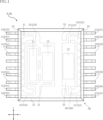
- FIG. 1 is a plan view of a semiconductor device according to a first embodiment of the present disclosure.
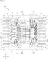
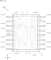
- FIG. 2 is a plan view corresponding to FIG. 1, showing the sealing resin through the plan view.
- FIG. 3 is a front view of the semiconductor device shown in FIG.
- FIG. 4 is a rear view of the semiconductor device shown in FIG.
- FIG. 5 is a left side view of the semiconductor device shown in FIG.
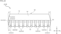
- FIG. 6 is a right side view of the semiconductor device shown in FIG.
- FIG. 7 is a cross-sectional view taken along line VII-VII in FIG.
- FIG. 8 is a cross-sectional view taken along line VIII-VIII in FIG.
- FIG. 9 is a cross-sectional view taken along line IX-IX in FIG.
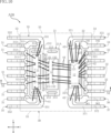
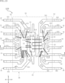
- FIG. 10 is a plan view of the semiconductor device according to the second embodiment of the present disclosure, seen through the sealing resin.
- FIG. 11 is a cross-sectional view taken along line XI-XI of FIG.
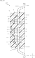
- FIG. 12 is a plan view of a semiconductor device according to a third embodiment of the present disclosure.
- FIG. 13 is a plan view corresponding to FIG. 12, showing the sealing resin through the transparent view.
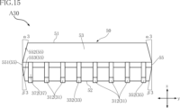
- 14 is a front view of the semiconductor device shown in FIG. 15 is a left side view of the semiconductor device shown in FIG.
- FIG. 16 is a cross-sectional view taken along line XVI-XVI in FIG.
- the semiconductor device A10 includes a first semiconductor element 11, a second semiconductor element 12, an insulating element 13, a first die pad 21, a second die pad 22, a plurality of first leads 31, a plurality of second leads 32, and a sealing resin 50.
- the semiconductor device A10 further includes a third lead 33, a fourth lead 34, a fifth lead 35, a sixth lead 36, two seventh leads 37, a plurality of first conductive members 41, a plurality of second conductive members 42, a plurality of third conductive members 43, and a plurality of fourth conductive members 44.
- the semiconductor device A10 is surface-mounted on a wiring board of an inverter device of an electric vehicle or a hybrid vehicle, for example.
- the package format of the semiconductor device A10 is a small outline package (SOP).
- SOP small outline package
- FIG. 2 shows the sealing resin 50 through the transparent state for ease of understanding.
- the outer shape of the sealing resin 50 is indicated by an imaginary line (two-dot chain line).
- first direction z A direction perpendicular to the first direction z is referred to as the "second direction x.”
- second direction x A direction perpendicular to both the first direction z and the second direction x is referred to as the "third direction y.”
- the first semiconductor element 11, the second semiconductor element 12, and the insulating element 13 are each composed of individual elements.
- the second semiconductor element 12 is located on the opposite side of the first semiconductor element 11 in the second direction x with the insulating element 13 as a reference.
- the insulating element 13 is located next to the first semiconductor element 11 in the third direction y.
- each of the first semiconductor element 11, the second semiconductor element 12, and the insulating element 13 is rectangular with its longer side extending in the third direction y.
- the first semiconductor element 11 controls the second semiconductor element 12.
- the first semiconductor element 11 includes a circuit that converts an electrical signal input from another semiconductor device into a PWM control signal, a transmission circuit that transmits the PWM control signal to the second semiconductor element 12, and a receiving circuit that receives the electrical signal from the second semiconductor element 12.
- the second semiconductor element 12 drives a switching element located outside the semiconductor device A10.
- the switching element is, for example, an IGBT (Insulated Gate Bipolar Transistor) or a MOSFET (Metal-Oxide-Semiconductor Field-Effect Transistor).
- the second semiconductor element 12 includes a receiving circuit for receiving a PWM control signal, a circuit for driving the switching element based on the PWM control signal, and a transmitting circuit for transmitting an electrical signal to the first semiconductor element 11.
- An example of the electrical signal is an output signal from a temperature sensor located near the motor.
- the insulating element 13 transmits an electric signal such as a PWM (Pulse Width Modulation) control signal in an insulated state.
- the insulating element 13 is an inductor-coupled type.
- An insulating transformer is an example of an inductor-coupled type insulating element 13.
- the insulating transformer transmits an electric signal in an insulated state by inductively coupling two inductors (coils).
- the two inductors include a transmitting inductor and a receiving inductor. Each of the two inductors is stacked in the first direction z.
- a dielectric layer made of silicon dioxide (SiO 2 ) or the like is located between the transmitting inductor and the receiving inductor. The dielectric layer electrically insulates the transmitting inductor and the receiving inductor.
- the insulating element 13 may be a capacitive type.
- a capacitor is an example of a capacitive type insulating element 13.
- the voltages applied to the first semiconductor element 11 and the second semiconductor element 12 are different from each other. Therefore, a potential difference occurs between the first semiconductor element 11 and the second semiconductor element 12.
- the voltage applied to the second semiconductor element 12 is higher than the voltage applied to the first semiconductor element 11.
- the power supply voltage supplied to the second semiconductor element 12 is higher than the power supply voltage supplied to the first semiconductor element 11.
- a first circuit having a first semiconductor element 11 and a second circuit having a second semiconductor element 12 are insulated from each other by an insulating element 13.
- the insulating element 13 is conductive to the first circuit and the second circuit.
- the first circuit includes a plurality of first leads 31, a third lead 33 and a fifth lead 35 in addition to the first semiconductor element 11.
- the second circuit includes a plurality of second leads 32, a fourth lead 34 and a sixth lead 36 in addition to the second die pad 22.
- the first circuit and the second circuit have relatively different potentials.
- the potential of the first circuit is higher than the potential of the second circuit.
- the insulating element 13 relays mutual signals between the first circuit and the second circuit.
- the voltage applied to the ground (GND) of the first semiconductor element 11 is about 0 V
- the voltage applied to the ground of the second semiconductor element 12 may transiently reach 600 V or more.
- the first semiconductor element 11 has a first element surface 11A that faces the same side in the first direction z as a first mounting surface 21A of a first die pad 21 described below.
- the first semiconductor element 11 has a plurality of first electrodes 111.
- the plurality of first electrodes 111 are provided on the first element surface 11A.
- the plurality of first electrodes 111 include, for example, aluminum (Al).
- the plurality of first electrodes 111 are conductive to a circuit formed in the first semiconductor element 11.
- the second semiconductor element 12 has a second element surface 12A that faces the same side in the first direction z as a second mounting surface 22A of the second die pad 22 described below.
- the second semiconductor element 12 has a plurality of second electrodes 121.
- the plurality of second electrodes 121 are provided on the second element surface 12A.
- the plurality of second electrodes 121 include, for example, aluminum.
- the plurality of second electrodes 121 are conductive to a circuit formed in the second semiconductor element 12.
- the insulating element 13 is located between the second semiconductor element 12 and the first semiconductor element 11 in the second direction x.
- the first semiconductor element 11 is located on the opposite side of the second semiconductor element 12 with respect to the insulating element 13 in the second direction x.
- On one side of the insulating element 13 in the first direction z (the side to which the first element surface 11A of the first semiconductor element 11 faces in the first direction z), a plurality of third electrodes 131 and a plurality of fourth electrodes 132 are provided.
- Each of the third electrodes 131 and each of the fourth electrodes 132 is conductive to a transmitting inductor or a receiving inductor, respectively.
- the multiple third electrodes 131 are arranged along the third direction y, and are located between the first semiconductor element 11 and the second semiconductor element 12 in the second direction x.
- the multiple fourth electrodes 132 are arranged along the third direction y, and are located on the opposite side of the first semiconductor element 11 with respect to the multiple third electrodes 131 in the second direction x.
- the multiple third electrodes 131 and the multiple fourth electrodes 132 include, for example, aluminum.
- the sealing resin 50 covers the first semiconductor element 11, the second semiconductor element 12, the insulating element 13, the first die pad 21, and the second die pad 22. As shown in FIG. 7, the sealing resin 50 further covers the first conductive members 41, the second conductive members 42, the third conductive members 43, and the fourth conductive members 44.
- the sealing resin 50 is an insulator.
- the sealing resin 50 is made of a material that contains, for example, epoxy resin. When viewed in the first direction z, the sealing resin 50 is rectangular.
- the sealing resin 50 has a top surface 51, a bottom surface 52, a first side surface 53, a second side surface 54, and two third side surfaces 55.
- the top surface 51 and the bottom surface 52 face in opposite directions in the first direction z.
- the top surface 51 faces the same side in the first direction z as the first mounting surface 21A of the first die pad 21, which will be described later.
- the first side 53 is connected to the top surface 51 and the bottom surface 52 and faces one side of the second direction x.
- the first side 53 is located closer to the first die pad 21 than the second side 54.
- the first side 53 includes a first region 531, a second region 532, and a third region 533.
- the first region 531 includes the first direction z as an in-plane direction. When viewed in the first direction z, the first region 531 is located outward from each of the top surface 51 and the bottom surface 52.
- the second region 532 is located between the first region 531 and the top surface 51 in the first direction z.
- the third region 533 is located on the opposite side to the second region 532 with respect to the first region 531.
- Each of the second region 532 and the third region 533 is inclined with respect to the first region 531.
- the inclination angle ⁇ 1 of the second region 532 relative to the first region 531 is greater than the inclination angle ⁇ 1 of the third region 533 relative to the first region 531.
- the second side 54 is connected to the top surface 51 and the bottom surface 52 and faces the opposite side to the first side 53 in the second direction x.
- the second side 54 is located closer to the second die pad 22 than the first side 53.
- the second side 54 includes a fourth region 541, a fifth region 542, and a sixth region 543.
- the fourth region 541 includes the first direction z as an in-plane direction. When viewed in the first direction z, the fourth region 541 is located outward from each of the top surface 51 and the bottom surface 52.
- the fifth region 542 is located between the fourth region 541 and the top surface 51 in the first direction z.
- the sixth region 543 is located on the opposite side to the fifth region 542 with respect to the fourth region 541.
- Each of the fifth region 542 and the sixth region 543 is inclined with respect to the fourth region 541.
- the inclination angle ⁇ 2 of the fifth region 542 relative to the fourth region 541 is greater than the inclination angle ⁇ 2 of the sixth region 543 relative to the fourth region 541.
- each of the two third side surfaces 55 is connected to the top surface 51 and the bottom surface 52 and faces opposite each other in the third direction y.
- Each of the two third side surfaces 55 includes a seventh region 551, an eighth region 552, and a ninth region 553.
- the seventh region 551 includes the first direction z as an in-plane direction. When viewed in the first direction z, the seventh region 551 is located outward from each of the top surface 51 and the bottom surface 52.
- the eighth region 552 is located between the seventh region 551 and the top surface 51 in the first direction z.
- the ninth region 553 is located on the opposite side to the eighth region 552 with respect to the seventh region 551.
- Each of the eighth region 552 and the ninth region 553 is inclined with respect to the seventh region 551.
- the inclination angle ⁇ 3 of the eighth region 552 relative to the seventh region 551 is greater than the inclination angle ⁇ 3 of the ninth region 553 relative to the seventh region 551.
- the first die pad 21, the second die pad 22, the multiple first leads 31, the multiple second leads 32, the third lead 33, the fourth lead 34, the fifth lead 35, the sixth lead 36, and the two seventh leads 37 all contain copper (Cu).
- the first die pad 21, the second die pad 22, and these leads are obtained from the same lead frame.
- the first die pad 21 and the second die pad 22 are spaced apart from each other in the second direction x, as shown in Figures 1 and 2.
- the first semiconductor element 11 and the insulating element 13 are mounted on the first die pad 21, and the second semiconductor element 12 is mounted on the second die pad 22.
- the area of the first die pad 21 is larger than the area of the second die pad 22 when viewed in the first direction z.
- the first semiconductor element 11 may be mounted on the first die pad 21, and the second semiconductor element 12 and the insulating element 13 may be mounted on the second die pad 22.
- the first die pad 21 has a first mounting surface 21A and a first back surface 21B that face opposite each other in the first direction z.
- the first mounting surface 21A faces the same side as the top surface 51 of the sealing resin 50 in the first direction z.
- the first semiconductor element 11 and the insulating element 13 are each bonded to the first mounting surface 21A via a bonding layer 29.
- the bonding layer 29 is made of a paste containing metal particles.
- the metal particles are, for example, silver (Ag). Therefore, the bonding layer 29 is a conductor. Alternatively, the bonding layer 29 may be solder.
- the distance in the first direction z between the first mounting surface 21A of the first die pad 21 and the top surface 51 of the sealing resin 50 is defined as a first distance D1.
- the distance in the first direction z between the first back surface 21B of the first die pad 21 and the bottom surface 52 of the sealing resin 50 is defined as a second distance D2.
- the distance in the first direction z between the first element surface 11A of the first semiconductor element 11 and the top surface 51 is defined as a third distance D3. In this case, the relationship D1>D2>D3 is satisfied.
- the first die pad 21 has two first holes 211, a plurality of second holes 212, and two third holes 213.
- the two first holes 211, the plurality of second holes 212, and the two third holes 213 each penetrate the first die pad 21 in the first direction z.
- the two first holes 211 are located on both sides of the first semiconductor element 11 in the third direction y.
- Each of the two first holes 211 extends in the second direction x.
- the plurality of second holes 212 are located between the first semiconductor element 11 and the insulating element 13 in the second direction x.
- Each of the plurality of second holes 212 extends in the third direction y.
- the plurality of second holes 212 are arranged along the third direction y.
- the two third holes 213 are located on both sides of the insulating element 13 in the third direction y. Each of the two third holes 213 extends in the second direction x.
- the second die pad 22 has a second mounting surface 22A and a second back surface 22B that face opposite each other in the first direction z.
- the second mounting surface 22A faces the same side as the first mounting surface 21A of the first die pad 21 in the first direction z.
- the second semiconductor element 12 is bonded to the second mounting surface 22A via a bonding layer 29.
- the distance in the first direction z between the second mounting surface 22A of the second die pad 22 and the top surface 51 of the sealing resin 50 is defined as a fourth distance D4.
- the distance in the first direction z between the second back surface 22B of the second die pad 22 and the bottom surface 52 of the sealing resin 50 is defined as a fifth distance D5.
- the distance in the first direction z between the second element surface 12A of the second semiconductor element 12 and the top surface 51 is defined as a sixth distance D6. In this case, the relationship D4>D5>D6 is satisfied.
- the multiple first leads 31 are located between the third lead 33 and the fifth lead 35 in the third direction y.
- the multiple first leads 31 are located on the opposite side of the second die pad 22 with respect to the first die pad 21 in the second direction x.
- the multiple first leads 31 are arranged along the third direction y. At least one of the multiple first leads 31 is electrically connected to the first semiconductor element 11.
- each of the multiple first leads 31 has a first inner part 311 and a first outer part 312.
- the first inner part 311 is covered with the sealing resin 50.
- the first inner part 311 has a first connection surface 311A.
- the first connection surface 311A faces the same side as the first mounting surface 21A of the first die pad 21 in the first direction z.
- the first connection surface 311A and the first mounting surface 21A are each included in the same plane.
- the first outer part 312 is connected to the first inner part 311.
- the first outer part 312 protrudes from the first region 531 of the first side surface 53 of the sealing resin 50. When viewed in the first direction z, the first outer part 312 extends in the second direction x.
- the first outer part 312 When viewed in the third direction y, the first outer part 312 is bent in a gull-wing shape.
- the shape of the first outer part 312 is equal to the shape of the third outer part 332 (see FIG. 4) of the third lead 33 described below.
- the surface of the first outer part 312 is plated with, for example, tin.
- the first outer part 312 has a first mounting surface 312A.
- the first mounting surface 312A faces the opposite side to the first connection surface 311A of the first inner part 311 in the first direction z.
- the first mounting surface 312A is located farthest from the first connection surface 311A in the first direction z.
- the first mounting surface 312A protrudes from within a plane including the bottom surface 52 of the sealing resin 50.
- the first mounting surface 312A is inclined with respect to the bottom surface 52.
- the third lead 33 includes a portion extending toward the first die pad 21 and is located closest to one of the two third side surfaces 55 of the sealing resin 50.
- the third lead 33 is connected to one side of the first die pad 21 in the third direction y.
- the third lead 33 is away from each of the two third side surfaces 55.
- the third lead 33 has a third inner part 331 and a third outer part 332.
- the third inner part 331 is connected to the first die pad 21 and is covered by the sealing resin 50.
- the third outer part 332 is connected to the third inner part 331.
- the third outer part 332 protrudes from a first region 531 of the first side surface 53 of the sealing resin 50. When viewed in the first direction z, the third outer part 332 extends in the second direction x. As shown in FIG. 4, the third outer part 332 is bent in a gull-wing shape when viewed in the third direction y.
- the surface of the third outer part 332 is, for example, tin-plated.
- the fifth lead 35 includes a portion extending toward the first die pad 21 and is located closest to one of the two third side surfaces 55 of the sealing resin 50.
- the fifth lead 35 is connected to the side of the first die pad 21 opposite to the side on which the third lead 33 is located in the third direction y.
- the fifth lead 35 is away from each of the two third side surfaces 55.
- the fifth lead 35 has a fifth inner part 351 and a fifth outer part 352.
- the fifth inner part 351 is connected to the first die pad 21 and is covered by the sealing resin 50.
- the fifth outer part 352 is connected to the fifth inner part 351.
- the fifth inner part 351 protrudes from the first region 531 of the first side surface 53 of the sealing resin 50.
- the fifth outer part 352 When viewed in the first direction z, the fifth outer part 352 extends in the second direction x. As shown in FIG. 3, the fifth outer part 352 is bent in a gull-wing shape when viewed in the third direction y.
- the surface of the fifth outer part 352 is, for example, tin-plated.
- the third inner portion 331 of the third lead 33 and the fifth inner portion 351 of the fifth lead 35 each overlap the first die pad 21.
- the multiple second leads 32 are located between the fourth lead 34 and the sixth lead 36 in the third direction y.
- the multiple second leads 32 are located on the opposite side of the first die pad 21 with respect to the second die pad 22 in the second direction x.
- the multiple second leads 32 are arranged along the third direction y. At least one of the multiple second leads 32 is electrically connected to the second semiconductor element 12.
- each of the multiple second leads 32 has a second inner part 321 and a second outer part 322.
- the second inner part 321 is covered with the sealing resin 50.
- the second inner part 321 has a second connection surface 321A.
- the second connection surface 321A faces the same side as the second mounting surface 22A of the second die pad 22 in the first direction z.
- the second connection surface 321A and the second mounting surface 22A are each included in the same plane.
- the second outer part 322 is connected to the second inner part 321.
- the second outer part 322 protrudes from the fourth region 541 of the second side surface 54 of the sealing resin 50. When viewed in the first direction z, the second outer part 322 extends in the second direction x.
- the second outer part 322 When viewed in the third direction y, the second outer part 322 is bent in a gull-wing shape.
- the shape of the second outer part 322 is equal to the shape of the seventh outer part 372 (see Figures 3 and 4) of each of the two seventh leads 37 described below.
- the surface of the second outer part 322 is, for example, tin-plated.
- the second outer part 322 has a second mounting surface 322A.
- the second mounting surface 322A faces the opposite side to the second connection surface 321A of the second inner part 321 in the first direction z.
- the second mounting surface 322A is located farthest from the second connection surface 321A in the first direction z.
- the second mounting surface 322A protrudes from within a plane including the bottom surface 52 of the sealing resin 50.
- the second mounting surface 322A is inclined with respect to the bottom surface 52.
- the fourth lead 34 includes a portion extending toward the second die pad 22 and is located closest to one of the two third side surfaces 55 of the sealing resin 50.
- the fourth lead 34 is connected to one side of the second die pad 22 in the third direction y.
- the fourth lead 34 is away from each of the two third side surfaces 55.
- the fourth lead 34 has a fourth inner part 341 and a fourth outer part 342.
- the fourth inner part 341 is connected to the second die pad 22 and is covered by the sealing resin 50.
- the fourth outer part 342 is connected to the fourth inner part 341.
- the fourth outer part 342 protrudes from the fourth region 541 of the second side surface 54 of the sealing resin 50. When viewed in the first direction z, the fourth outer part 342 extends in the second direction x.
- the fourth outer part 342 When viewed in the third direction y, the fourth outer part 342 is bent in a gull-wing shape.
- the shape of the fourth outer part 342 is equal to the shape of the seventh outer part 372 (see Figures 3 and 4) of each of the two seventh leads 37 described below.
- the surface of the fourth outer part 342 is, for example, tin-plated.
- the sixth lead 36 includes a portion extending toward the second die pad 22 and is located closest to one of the two third side surfaces 55 of the sealing resin 50.
- the sixth lead 36 is connected to the side of the second die pad 22 opposite to the side on which the fourth lead 34 is located in the third direction y.
- the sixth lead 36 is away from each of the two third side surfaces 55.
- the sixth lead 36 has a sixth inner part 361 and a sixth outer part 362.
- the sixth inner part 361 is connected to the second die pad 22 and is covered by the sealing resin 50.
- the sixth outer part 362 is connected to the sixth inner part 361.
- the sixth outer part 362 protrudes from the fourth region 541 of the second side surface 54 of the sealing resin 50.
- the sixth outer part 362 When viewed in the first direction z, the sixth outer part 362 extends in the second direction x.
- the sixth outer part 362 is bent in a gull-wing shape when viewed in the third direction y.
- the shape of the sixth outer part 362 is equal to the shape of the seventh outer part 372 (see Figures 3 and 4) of each of the two seventh leads 37 described below.
- the fourth inner portion 341 of the fourth lead 34 and the sixth inner portion 361 of the sixth lead 36 each overlap the second die pad 22.
- each of the two seventh leads 37 includes a portion extending toward either the first die pad 21 or the second die pad 22, and is located closest to either of the two third side surfaces 55 of the sealing resin 50.
- the two seventh leads 37 are spaced apart from each other in the third direction y.
- a plurality of second leads 32, fourth leads 34, and sixth leads 36 are located between the two seventh leads 37.
- Each of the two seventh leads 37 is spaced apart from each of the first die pad 21, the second die pad 22, and the two third side surfaces 55.
- Each of the two seventh leads 37 has a seventh inner portion 371 and a seventh outer portion 372.
- the seventh inner portion 371 is covered with the sealing resin 50.
- the seventh outer portion 372 is connected to the seventh inner portion 371.
- the seventh outer part 372 protrudes from the fourth region 541 of the second side surface 54 of the sealing resin 50. When viewed in the first direction z, the seventh outer part 372 extends in the second direction x. As shown in FIGS. 3 and 4, the seventh outer part 372 is bent in a gull-wing shape when viewed in the third direction y.
- the surface of the seventh outer part 372 is, for example, tin-plated.
- each of the multiple first conductive members 41 is conductively joined to one of the multiple first electrodes 111 of the first semiconductor element 11 and the first connection surface 311A of the first inner portion 311 of one of the multiple first leads 31.
- at least one of the multiple first leads 31 is conductively connected to the first semiconductor element 11.
- At least one of the multiple first conductive members 41 is conductively joined to one of the multiple first electrodes 111 and the third inner portion 331 of the third lead 33.
- the third lead 33 is conductively connected to the first semiconductor element 11.
- at least one of the multiple first conductive members 41 is conductively joined to one of the multiple first electrodes 111 and the fifth inner portion 351 of the fifth lead 35.
- the fifth lead 35 is conductively connected to the first semiconductor element 11.
- At least one of the third lead 33 and the fifth lead 35 forms the ground of the first semiconductor element 11.
- the multiple first conductive members 41 are located between the first mounting surface 21A of the first die pad 21 and the top surface 51 of the sealing resin 50.
- the multiple first conductive members 41 are wires.
- the multiple first conductive members 41 contain, for example, gold.
- each of the multiple first conductive members 41 may include a core material containing copper and a coating material containing palladium and covering the core material.
- each of the multiple second conductive members 42 is conductively joined to one of the multiple second electrodes 121 of the second semiconductor element 12 and the second connection surface 321A of the second inner portion 321 of one of the multiple second leads 32.
- at least one of the multiple second leads 32 is conductively connected to the second semiconductor element 12.
- At least one of the multiple second conductive members 42 is conductively joined to one of the multiple second electrodes 121 and the fourth inner portion 341 of the fourth lead 34.
- the fourth lead 34 is conductively connected to the second semiconductor element 12.
- At least one of the multiple second conductive members 42 is conductively joined to one of the multiple second electrodes 121 and the sixth inner portion 361 of the sixth lead 36.
- the sixth lead 36 is conductively connected to the second semiconductor element 12. At least one of the fourth lead 34 and the sixth lead 36 forms the ground of the second semiconductor element 12. At least one of the multiple second conductive members 42 is conductively joined to one of the multiple second electrodes 121 and to the seventh inner portion 371 of one of the two seventh leads 37. As a result, one of the two seventh leads 37 is electrically connected to the second semiconductor element 12.
- the multiple second conductive members 42 are located between the second mounting surface 22A of the second die pad 22 and the top surface 51 of the sealing resin 50.
- the multiple second conductive members 42 are wires.
- the multiple second conductive members 42 contain, for example, gold.
- each of the multiple second conductive members 42 may include a core material containing copper and a coating material containing palladium and covering the core material.
- each of the multiple third conductive members 43 is conductively joined to one of the multiple third electrodes 131 of the insulating element 13 and one of the multiple first electrodes 111 of the first semiconductor element 11. This allows the first semiconductor element 11 to be electrically connected to the insulating element 13.
- the multiple third conductive members 43 are arranged along the third direction y. Any of the multiple third conductive members 43 straddles any of the multiple second holes 212 provided in the first die pad 21.
- each of the multiple fourth conductive members 44 is conductively joined to one of the multiple fourth electrodes 132 of the insulating element 13 and one of the multiple second electrodes 121 of the second semiconductor element 12. This allows the second semiconductor element 12 to be electrically connected to the insulating element 13.
- the multiple fourth conductive members 44 are arranged along the third direction y. The multiple fourth conductive members 44 straddle the gap between the first die pad 21 and the second die pad 22.
- each of the multiple third conductive members 43 and the multiple fourth conductive members 44 is located between either the first mounting surface 21A of the first die pad 21 or the second mounting surface 22A of the second die pad 22 and the top surface 51 of the sealing resin 50.
- the multiple third conductive members 43 and the multiple fourth conductive members 44 are wires.
- the multiple third conductive members 43 and the multiple fourth conductive members 44 contain, for example, gold.
- the distance L1 from the top surface 51 of the sealing resin 50 to any one of the multiple fourth conductive members 44 is shorter than the distance L2 from the top surface 51 to any one of the multiple third conductive members 43.
- a half-bridge circuit including a low-side (low potential side) switching element and a high-side (high potential side) switching element is generally configured.
- these switching elements are MOSFETs.
- the reference potential of the source of the switching element and the gate driver that drives the switching element are both ground.
- the reference potential of the source of the switching element and the gate driver that drives the switching element are both equivalent to the potential at the output node of the half-bridge circuit.
- the reference potential of the gate driver that drives the high-side switching element changes.
- the reference potential is equivalent to the voltage applied to the drain of the high-side switching element (for example, 600 V or more).
- the ground of the first semiconductor element 11 and the ground of the second semiconductor element 12 are configured to be separated. Therefore, when the semiconductor device A10 is used as a gate driver for driving a high-side switching element, a voltage equivalent to the voltage applied to the drain of the high-side switching element is transiently applied to the ground of the second semiconductor element 12.
- the semiconductor device A10 includes a first die pad 21, a first semiconductor element 11, a first lead 31, a first conductive member 41, and a sealing resin 50.
- the first lead 31 protrudes from a first side surface 53 of the sealing resin 50.
- the distance in the first direction z between the first mounting surface 21A of the first die pad 21 and the top surface 51 of the sealing resin 50 is defined as a first distance D1.
- the distance in the first direction z between the first back surface 21B of the first die pad 21 and the bottom surface 52 of the sealing resin 50 is defined as a second distance D2.
- the distance in the first direction z between the first element surface 11A of the first semiconductor element 11 and the top surface 51 is defined as a third distance D3.
- the first conductive member 41 is located between the first mounting surface 21A and the top surface 51.
- the sealing resin 50 that covers the first conductive member 41 can be made larger without increasing the size of the sealing resin 50. Therefore, with this configuration, in the semiconductor device A10, it is possible to suppress a decrease in the dielectric strength voltage of the semiconductor device A10 without increasing the size of the semiconductor device A10.
- the first side surface 53 of the sealing resin 50 includes a first region 531, a second region 532, and a third region 533.
- the second region 532 and the third region 533 are each inclined with respect to the first region 531.
- the first lead 31 protrudes from the first region 531.
- the inclination angle ⁇ 1 of the second region 532 with respect to the first region 531 is greater than the inclination angle ⁇ 1 of the third region 533 with respect to the first region 531.
- the semiconductor device A10 further includes a second die pad 22, a second semiconductor element 12, a second lead 32, and a second conductive member 42.
- the second lead 32 protrudes from the second side surface 54 of the sealing resin 50.
- the distance in the first direction z between the second mounting surface 22A of the second die pad 22 and the top surface 51 of the sealing resin 50 is a fourth distance D4.
- the distance in the first direction z between the second back surface 22B of the second die pad 22 and the bottom surface 52 of the sealing resin 50 is a fifth distance D5.
- the distance in the first direction z between the second element surface 12A of the second semiconductor element 12 and the top surface 51 is a sixth distance D6.
- the second conductive member 42 is located between the second mounting surface 22A and the top surface 51.
- the covering of the sealing resin 50 that covers the second conductive member 42 can be made larger without increasing the size of the sealing resin 50. This effectively prevents a decrease in the dielectric strength voltage of the semiconductor device A10.
- the third lead 33 and the fifth lead 35 each overlap the first die pad 21.
- This configuration makes the flow rate of the molten resin that flows on both sides of the first die pad 21 in the cavity of the molding die in the first direction z more uniform. This makes the filling state of the portion of the sealing resin 50 that overlaps the entire first die pad 21 more dense when viewed in the first direction z.
- each of the two seventh leads 37 overlaps the second die pad 22.
- This configuration makes the flow rate of the molten resin flowing on both sides of the second die pad 22 in the first direction z in the cavity of the molding die more uniform. This makes the filling state of the portion of the sealing resin 50 that overlaps the entire second die pad 22 more dense when viewed in the first direction z.
- the semiconductor device A10 further includes an insulating element 13, a third conductive member 43, and a fourth conductive member 44.
- each of the third conductive member 43 and the fourth conductive member 44 is located between either the first mounting surface 21A of the first die pad 21 or the second mounting surface 22A of the second die pad 22 and the top surface 51 of the sealing resin 50.
- This configuration makes it possible to increase the area of the sealing resin 50 covering the third conductive member 43 and the area of the sealing resin 50 covering the fourth conductive member 44 without increasing the size of the sealing resin 50. This makes it possible to more effectively suppress a decrease in the dielectric strength voltage of the semiconductor device A10.
- the first die pad 21 has two first holes 211 and a second hole 212 that each penetrate in the first direction z.
- the two first holes 211 are located on either side of the first semiconductor element 11 in the third direction y.
- the second hole 212 is located between the first semiconductor element 11 and the insulating element 13 in the second direction x.
- FIG. 10 shows the sealing resin 50 in a see-through manner for ease of understanding.
- the outline of the sealing resin 50 is shown by imaginary lines.
- semiconductor device A20 the configuration of the multiple first leads 31 and multiple second leads 32 differs from that of semiconductor device A10.
- the top surface 51 of the sealing resin 50 is located closer to the first connection surface 311A of each of the first leads 31 than the first mounting surface 21A of the first die pad 21.
- the top surface 51 is located closer to the second connection surface 321A of each of the second leads 32 than the second mounting surface 22A of the second die pad 22.
- the semiconductor device A20 includes a first die pad 21, a first semiconductor element 11, a first lead 31, a first conductive member 41, and a sealing resin 50.
- the first lead 31 protrudes from a first side surface 53 of the sealing resin 50.
- the distance between the first mounting surface 21A of the first die pad 21 and the top surface 51 of the sealing resin 50 in the first direction z is defined as a first distance D1.
- the distance between the first back surface 21B of the first die pad 21 and the bottom surface 52 of the sealing resin 50 in the first direction z is defined as a second distance D2.
- the third distance between the first element surface 11A of the first semiconductor element 11 and the top surface 51 in the first direction z is defined as D3.
- the first conductive member 41 is located between the first mounting surface 21A and the top surface 51. Therefore, with this configuration, it is possible to suppress the decrease in the dielectric strength voltage of the semiconductor device A20 without increasing the size of the semiconductor device A20. Furthermore, the semiconductor device A20 has a configuration in common with the semiconductor device A10, and thus achieves the same effects as the semiconductor device A10.
- the top surface 51 of the sealing resin 50 is located closer to the first connection surface 311A of the first lead 31 than the first mounting surface 21A of the first die pad 21.
- FIG. 12 shows the sealing resin 50 in a see-through manner.
- the outline of the sealing resin 50 is shown by imaginary lines.
- the configuration of the third lead 33 is different from that of semiconductor device A10.
- the third inner portion 331 of the third lead 33 is connected to one side of the first die pad 21 in the second direction x.
- the third lead 33 is located between two of the multiple first leads 31 in the third direction y.
- the third lead 33 is located on the opposite side of the second die pad 22 with respect to the first die pad 21 in the second direction x.
- the semiconductor device A30 has one seventh lead 37 instead of two seventh leads 37.
- the seventh lead 37 is located on one side of the first die pad 21 in the third direction y.
- the multiple first leads 31 and the third lead 33 are located between the seventh lead 37 and the fifth lead 35 in the third direction y.
- the semiconductor device A30 includes a first die pad 21, a first semiconductor element 11, a first lead 31, a first conductive member 41, and a sealing resin 50.
- the first lead 31 protrudes from a first side surface 53 of the sealing resin 50.
- the distance between the first mounting surface 21A of the first die pad 21 and the top surface 51 of the sealing resin 50 in the first direction z is defined as a first distance D1.
- the distance between the first back surface 21B of the first die pad 21 and the bottom surface 52 of the sealing resin 50 in the first direction z is defined as a second distance D2.
- the third distance between the first element surface 11A of the first semiconductor element 11 and the top surface 51 in the first direction z is defined as D3.
- the first conductive member 41 is located between the first mounting surface 21A and the top surface 51. Therefore, with this configuration, it is possible to suppress the decrease in the dielectric strength voltage of the semiconductor device A30 without increasing the size of the semiconductor device A30. Furthermore, the semiconductor device A30 has a configuration in common with the semiconductor device A10, and thus achieves the same effects as the semiconductor device A10.
- Appendix 1 a first die pad having a first mounting surface and a first back surface facing in opposite directions in a first direction; a first semiconductor element mounted on the first mounting surface; a first lead spaced from the first die pad; a first conductive member conductively connected to the first semiconductor element and the first lead; a sealing resin that covers the first die pad, the first semiconductor element, and the first conductive member, the first semiconductor element has a first element surface facing the same side as the first mounting surface in the first direction; the sealing resin has a top surface facing the same side as the first mounting surface in the first direction, a bottom surface facing an opposite side to the top surface in the first direction, and a first side surface facing one side in a second direction perpendicular to the first direction, the first lead protrudes from the first side surface, When a first distance between the first mounting surface and the top surface in the first direction is defined as D1, a second distance between the first back surface and the bottom surface in the first direction is defined as D
- the first side includes a first region including the first direction as an in-plane direction, a second region located between the first region and the top surface in the first direction, and a third region located on the opposite side of the second region with respect to the first region; each of the second region and the third region is inclined with respect to the first region; the first lead protrudes from the first region; 2.
- the semiconductor device of claim 1 wherein an inclination angle of the second region with respect to the first region is greater than an inclination angle of the third region with respect to the first region.
- Appendix 3. 3.
- the first conductive member is a wire.
- the first lead has a first connection surface facing the same side as the first mounting surface in the first direction; 4.
- the semiconductor device according to claim 3, wherein the first conductive member is conductively connected to the first connection surface. Appendix 5. 5. The semiconductor device according to claim 4, wherein the first connection surface and the first mounting surface are included in the same plane. Appendix 6. 5. The semiconductor device of claim 4, wherein the top surface is located closer to the first connection surface than the first mounting surface. Appendix 7. the first lead has a first mounting surface that is exposed from the sealing resin and faces an opposite side to the first connection surface in the first direction; the first mounting surface is located farthest from the first connecting surface in the first direction, 5. The semiconductor device according to claim 4, wherein the first mounting surface protrudes from a plane including the bottom surface. Appendix 8. 8. The semiconductor device according to claim 7, wherein the first mounting surface is inclined with respect to the bottom surface.
- Appendix 9 a second die pad having a second mounting surface facing the same side as the first mounting surface in the first direction and a second back surface facing an opposite side to the second mounting surface in the first direction; A second semiconductor element mounted on the second mounting surface; a second lead spaced from the second die pad; a second conductive member conductively connected to the second semiconductor element and the second lead, the second semiconductor element has a second element surface facing the same side as the second mounting surface in the first direction, the sealing resin has a second side surface facing an opposite side to the first side surface in the second direction, the second die pad, the second semiconductor element, and the second conductive member are covered with the sealing resin; the second lead protrudes from the second side surface,
- D4 a fourth distance between the second mounting surface and the top surface in the first direction
- D5 a fifth distance between the second back surface and the bottom surface in the first direction
- D6 a sixth distance between the second element surface and the top surface in the first direction
- the second conductive member is located between the second mounting surface and the top surface.
- Appendix 10. 10. The semiconductor device according to claim 9, wherein the second conductive member is a wire.
- Appendix 11. a third lead connected to the first die pad; 11. The semiconductor device according to claim 10, wherein the third lead protrudes from the first side surface.
- Appendix 12. the sealing resin has two third side surfaces spaced apart from each other in a third direction perpendicular to each of the first direction and the second direction; 12.
- the semiconductor device of claim 11, wherein the third lead is spaced apart from each of the two third sides.
- Appendix 13. 13 The semiconductor device according to claim 12, wherein the third lead is coupled to one side of the first die pad in the first direction. Appendix 14.
- a fourth lead connected to the second die pad; 13.
- Appendix 15. The semiconductor device of claim 14, wherein the fourth lead is spaced apart from each of the two third sides.
- Appendix 16. an insulating element mounted on the first mounting surface; a third conductive member conductively connected to the insulating element and the first semiconductor element; a fourth conductive member conductively connected to the insulating element and the second semiconductor element, In the first direction, each of the third conductive member and the fourth conductive member is located between either the first mounting surface or the second mounting surface and the top surface, 16.
- Appendix 17. 17 The semiconductor device according to claim 16, wherein a distance from the top surface to the fourth conductive member in the first direction is shorter than a distance from the top surface to the third conductive member.
Landscapes
- Structures Or Materials For Encapsulating Or Coating Semiconductor Devices Or Solid State Devices (AREA)
Abstract
半導体装置は、第1ダイパッド、第1半導体素子、第1リード、第1導通部材および封止樹脂を備える。前記第1導通部材は、前記第1半導体素子と前記第1リードとに導電接合されている。前記第1ダイパッド、前記第1半導体素子および前記第1導通部材は、前記封止樹脂に覆われている。前記第1リードは、前記封止樹脂の第1側面から突出している。第1距離D1、第2距離D2および第3距離D3は、D1>D2≧D3の関係を満たす。第1方向zにおいて、第1導通部材41は、第1ダイパッド21の第1搭載面21Aと封止樹脂50の頂面51との間に位置する。
Description
本開示は、半導体装置に関する。
特許文献1に開示されている半導体装置は、2つのダイパッドと、2つのダイパッドに個別に搭載された制御素子(コントローラ)および駆動素子(ゲートドライバ)と、2つのダイパッド、制御素子および駆動素子を覆う封止樹脂とを備える。当該半導体装置は、IGBTやMOSFETなどのスイッチング素子を駆動する。当該半導体装置は、インバータ回路などに用いられる。
ここで、当該半導体装置においては、駆動素子に供給される電源電圧は、スイッチング素子に印加される電圧以上であるため、制御素子に供給される電源電圧と、駆動素子に供給される電源電圧とは異なる。このため、制御素子およびその導電経路に印加される電圧と、駆動素子およびその導電経路に印加される電圧とに差異が生じる。そこで、当該半導体装置においては、制御素子と駆動素子との間の電気信号の伝送経路に絶縁素子を介在させることによって、制御素子およびその導電経路と、駆動素子およびその導電経路とが互いに絶縁されている。これにより、制御素子および駆動素子の各々が絶縁破壊することが防止される。
当該半導体装置においては、制御素子および駆動素子のいずれかと端子とに導電接合されたワイヤをさらに備える。ここで、当該半導体装置の大きさをより小さくする、または当該半導体装置の大きさを変えずに制御素子および駆動素子の各々の大きさをより大きくすると、ワイヤを覆う封止樹脂の被りがより小さくなる。当該被りが小さくなると、当該半導体装置の絶縁耐圧の低下が懸念される。
概要:
本開示は、従来より改良が施された半導体装置を提供することを一の課題とする。特に本開示は、先述の事情に鑑み、装置の大型化を招くことなく、当該装置の絶縁耐圧の低下を抑制することが可能な半導体装置を提供することを一の課題とする。
本開示は、従来より改良が施された半導体装置を提供することを一の課題とする。特に本開示は、先述の事情に鑑み、装置の大型化を招くことなく、当該装置の絶縁耐圧の低下を抑制することが可能な半導体装置を提供することを一の課題とする。
本開示の第1の側面によって提供される半導体装置は、第1方向において互いに反対側を向く第1搭載面および第1裏面を有する第1ダイパッドと、前記第1搭載面に搭載された第1半導体素子と、前記第1ダイパッドから離れた第1リードと、前記第1半導体素子と前記第1リードとに導電接合された第1導通部材と、前記第1ダイパッド、前記第1半導体素子および前記第1導通部材を覆う封止樹脂とを備える。前記第1半導体素子は、前記第1方向において前記第1搭載面と同じ側を向く第1素子面を有する。前記封止樹脂は、前記第1方向において前記第1搭載面と同じ側を向く頂面と、前記第1方向において前記頂面とは反対側を向く底面と、前記第1方向に対して直交する第2方向の一方側を向く第1側面とを有する。前記第1リードは、前記第1側面から突出している。前記第1方向における前記第1搭載面と前記頂面との第1間隔をD1、前記第1方向における前記第1裏面と前記底面との第2間隔をD2、前記第1方向における前記第1素子面と前記頂面との第3間隔をD3、とすると、D1>D2≧D3の関係を満たす。前記第1方向において、前記第1導通部材は、前記第1搭載面と前記頂面との間に位置する。
本開示のその他の特徴および利点は、添付図面に基づき以下に行う詳細な説明によって、より明らかとなろう。
詳細な説明:
本開示の詳細について、添付図面に基づき説明する。
本開示の詳細について、添付図面に基づき説明する。
第1実施形態:
図1~図9に基づき、本開示の第1実施形態にかかる半導体装置A10について説明する。半導体装置A10は、第1半導体素子11、第2半導体素子12、絶縁素子13、第1ダイパッド21、第2ダイパッド22、複数の第1リード31、複数の第2リード32、および封止樹脂50を備える。さらに半導体装置A10は、第3リード33、第4リード34、第5リード35、第6リード36、2つの第7リード37、複数の第1導通部材41、複数の第2導通部材42、複数の第3導通部材43、および複数の第4導通部材44を備える。半導体装置A10は、たとえば電気自動車またはハイブリッド自動車などのインバータ装置の配線基板に表面実装されるものである。半導体装置A10のパッケージ形式は、SOP(Small Outline Package)である。ただし、半導体装置A10のパッケージ形式は、SOPに限定されない。ここで、図2は、理解の便宜上、封止樹脂50を透過して示している。図2においては、封止樹脂50の外形を想像線(二点鎖線)で示している。
図1~図9に基づき、本開示の第1実施形態にかかる半導体装置A10について説明する。半導体装置A10は、第1半導体素子11、第2半導体素子12、絶縁素子13、第1ダイパッド21、第2ダイパッド22、複数の第1リード31、複数の第2リード32、および封止樹脂50を備える。さらに半導体装置A10は、第3リード33、第4リード34、第5リード35、第6リード36、2つの第7リード37、複数の第1導通部材41、複数の第2導通部材42、複数の第3導通部材43、および複数の第4導通部材44を備える。半導体装置A10は、たとえば電気自動車またはハイブリッド自動車などのインバータ装置の配線基板に表面実装されるものである。半導体装置A10のパッケージ形式は、SOP(Small Outline Package)である。ただし、半導体装置A10のパッケージ形式は、SOPに限定されない。ここで、図2は、理解の便宜上、封止樹脂50を透過して示している。図2においては、封止樹脂50の外形を想像線(二点鎖線)で示している。
半導体装置A10の説明においては、便宜上、後述する第1ダイパッド21の第1搭載面21Aの法線方向を「第1方向z」と呼ぶ。第1方向zに対して直交する一方向を「第2方向x」と呼ぶ。第1方向zおよび第2方向xの各々に対して直交する方向を「第3方向y」と呼ぶ。
半導体装置A10においては、第1半導体素子11、第2半導体素子12および絶縁素子13は、それぞれ個々の素子で構成されている。第2半導体素子12は、第2方向xにおいて絶縁素子13を基準として第1半導体素子11とは反対側に位置する。絶縁素子13は、第3方向yにおいて第1半導体素子11の隣に位置する。第1方向zに視て(平面視において)、第1半導体素子11、第2半導体素子12および絶縁素子13の各々は、第3方向yを長辺とする矩形状である。
第1半導体素子11は、第2半導体素子12を制御する。第1半導体素子11は、他の半導体装置から入力された電気信号をPWM制御信号に変換する回路と、当該PWM制御信号を第2半導体素子12へ伝送するための送信回路と、第2半導体素子12からの電気信号を受ける受信回路とを具備する。
第2半導体素子12は、半導体装置A10の外部に位置するスイッチング素子を駆動する。スイッチング素子は、たとえばIGBT(Insulated Gate Bipolar Transistor)やMOSFET(Metal-Oxide-Semiconductor Field-Effect Transistor)である。第2半導体素子12は、PWM制御信号を受信する受信回路と、当該PWM制御信号に基づきスイッチング素子を駆動するための回路と、電気信号を第1半導体素子11へ伝送するための送信回路とを具備する。当該電気信号は、たとえばモータ近傍に配置された温度センサからの出力信号が挙げられる。
絶縁素子13は、PWM(Pulse Width Modulation)制御信号などの電気信号を絶縁状態で伝送する。絶縁素子13は、インダクタ結合型である。インダクタ結合型の絶縁素子13の一例として、絶縁型トランスが挙げられる。絶縁型トランスは、2つのインダクタ(コイル)を誘導結合させることで、絶縁状態による電気信号の伝送を行う。当該2つのインダクタは、送信側インダクタおよび受信側インダクタを含む。当該2つのインダクタの各々は、第1方向zに積層されている。送信側インダクタと受信側インダクタとの間には、二酸化ケイ素(SiO2)などからなる誘電体層が位置する。当該誘電体層により、送信側インダクタと受信側インダクタとは、電気絶縁されている。この他、絶縁素子13は、キャパシティブ型でよい。キャパシティブ型の絶縁素子13の一例として、コンデンサが挙げられる。
第1半導体素子11および第2半導体素子12の各々に印加される電圧は、互いに異なる。このため、第1半導体素子11と第2半導体素子12との間に電位差が生じる。半導体装置A10においては、第2半導体素子12に印加される電圧は、第1半導体素子11に印加される電圧より高い。あわせて半導体装置A10においては、第2半導体素子12に供給される電源電圧は、第1半導体素子11に供給される電源電圧より高い。
半導体装置A10においては、第1半導体素子11を具備する第1回路と、第2半導体素子12を具備する第2回路とが、絶縁素子13により互いに絶縁されている。絶縁素子13は、第1回路と第2回路とに導通している。第1回路は、第1半導体素子11の他、複数の第1リード31、第3リード33および第5リード35を含む。第2回路は、第2ダイパッド22の他、複数の第2リード32、第4リード34および第6リード36を含む。第1回路と第2回路とは、相対的に電位が異なる。半導体装置A10においては、第1回路の電位は、第2回路の電位より高い。絶縁素子13は、第1回路と第2回路との間の相互信号を中継する。たとえば、電気自動車やハイブリッド自動車のインバータ装置においては、第1半導体素子11のグランド(GND)に印加させる電圧が0V程度であることに対し、第2半導体素子12のグランドに印加される電圧が過渡的に600V以上となることがある。
図7に示すように、第1半導体素子11は、後述する第1ダイパッド21の第1搭載面21Aと第1方向zにおいて同じ側を向く第1素子面11Aを有する。図2および図7に示すように、第1半導体素子11は、複数の第1電極111を有する。複数の第1電極111は、第1素子面11Aに設けられている。複数の第1電極111は、たとえばアルミニウム(Al)を含む。複数の第1電極111は、第1半導体素子11に構成された回路に導通している。
図7に示すように、第2半導体素子12は、後述する第2ダイパッド22の第2搭載面22Aと第1方向zにおいて同じ側を向く第2素子面12Aを有する。図2、図7および図9に示すように、第2半導体素子12は、複数の第2電極121を有する。複数の第2電極121は、第2素子面12Aに設けられている。複数の第2電極121は、たとえばアルミニウムを含む。複数の第2電極121は、第2半導体素子12に構成された回路に導通している。
図2および図7示すように、絶縁素子13は、第2方向xにおいて、第2半導体素子12と第1半導体素子11との間に位置する。換言すれば、第1半導体素子11は、第2方向xにおいて絶縁素子13を基準として第2半導体素子12とは反対側に位置する。絶縁素子13の第1方向zの一方側(第1方向zにおいて第1半導体素子11の第1素子面11Aが向く側)には、複数の第3電極131、および複数の第4電極132が設けられている。各第3電極131および各第4電極132は、送信側インダクタまたは受信側インダクタにそれぞれ導通している。複数の第3電極131は、第3方向yに沿って配列され、かつ第2方向xにおいて第1半導体素子11と第2半導体素子12との間に位置する。複数の第4電極132は、第3方向yに沿って配列され、かつ第2方向xにおいて複数の第3電極131を基準として第1半導体素子11とは反対側に位置する。複数の第3電極131、および複数の第4電極132は、たとえばアルミニウムを含む。
封止樹脂50は、図1に示すように、第1半導体素子11、第2半導体素子12、絶縁素子13、第1ダイパッド21および第2ダイパッド22を覆っている。図7に示すように、封止樹脂50は、複数の第1導通部材41、複数の第2導通部材42、複数の第3導通部材43、および複数の第4導通部材44をさらに覆っている。封止樹脂50は、絶縁体である。封止樹脂50は、たとえばエポキシ樹脂を含む材料からなる。第1方向zに視て、封止樹脂50は矩形状である。
図3~図6に示すように、封止樹脂50は、頂面51、底面52、第1側面53、第2側面54、および2つの第3側面55を有する。
図3~図6に示すように、頂面51および底面52は、第1方向zにおいて互いに反対側を向く。頂面51は、第1方向zにおいて後述する第1ダイパッド21の第1搭載面21Aと同じ側を向く。
図3および図4に示すように、第1側面53は、頂面51および底面52につながるとともに、第2方向xの一方側を向く。第1側面53は、第2側面54より第1ダイパッド21の近くに位置する。第1側面53は、第1領域531、第2領域532および第3領域533を含む。第1領域531は、面内方向として第1方向zを含む。第1方向zに視て、第1領域531は、頂面51および底面52の各々より外方に位置する。第2領域532は、第1方向zにおいて第1領域531と頂面51との間に位置する。第3領域533は、第1領域531を基準として第2領域532とは反対側に位置する。第2領域532および第3領域533の各々は、第1領域531に対して傾斜している。第1領域531に対する第2領域532の傾斜角α1は、第1領域531に対する第3領域533の傾斜角β1より大きい。
図3および図4に示すように、第2側面54は、頂面51および底面52につながるとともに、第2方向xにおいて第1側面53とは反対側を向く。第2側面54は、第1側面53より第2ダイパッド22の近くに位置する。第2側面54は、第4領域541、第5領域542および第6領域543を含む。第4領域541は、面内方向として第1方向zを含む。第1方向zに視て、第4領域541は、頂面51および底面52の各々より外方に位置する。第5領域542は、第1方向zにおいて第4領域541と頂面51との間に位置する。第6領域543は、第4領域541を基準として第5領域542とは反対側に位置する。第5領域542および第6領域543の各々は、第4領域541に対して傾斜している。第4領域541に対する第5領域542の傾斜角α2は、第4領域541に対する第6領域543の傾斜角β2より大きい。
図5および図6に示すように、2つの第3側面55の各々は、頂面51および底面52につながるとともに、第3方向yにおいて互いに反対側を向く。2つの第3側面55の各々は、第7領域551、第8領域552および第9領域553を含む。第7領域551は、面内方向として第1方向zを含む。第1方向zに視て、第7領域551は、頂面51および底面52の各々より外方に位置する。第8領域552は、第1方向zにおいて第7領域551と頂面51との間に位置する。第9領域553は、第7領域551を基準として第8領域552とは反対側に位置する。第8領域552および第9領域553の各々は、第7領域551に対して傾斜している。第7領域551に対する第8領域552の傾斜角α3は、第7領域551に対する第9領域553の傾斜角β3より大きい。
第1ダイパッド21、第2ダイパッド22、複数の第1リード31、複数の第2リード32、第3リード33、第4リード34、第5リード35、第6リード36、および2つの第7リード37は、いずれも銅(Cu)を含む。第1ダイパッド21、第2ダイパッド22、およびこれらのリードは、同一のリードフレームから得られる。
第1ダイパッド21および第2ダイパッド22は、図1および図2に示すように、第2方向xにおいて互いに離れている。半導体装置A10においては、第1半導体素子11および絶縁素子13が第1ダイパッド21に搭載され、かつ第2半導体素子12が第2ダイパッド22に搭載されている。この場合において、第1方向zに視て、第1ダイパッド21の面積は、第2ダイパッド22の面積より大きい。図示された例とは異なり、第1半導体素子11が第1ダイパッド21に搭載され、かつ第2半導体素子12および絶縁素子13が第2ダイパッド22に搭載されてよい。
図7および図8に示すように、第1ダイパッド21は、第1方向zにおいて互いに反対側を向く第1搭載面21Aおよび第1裏面21Bを有する。第1搭載面21Aは、第1方向zにおいて封止樹脂50の頂面51と同じ側を向く。第1半導体素子11および絶縁素子13の各々は、接合層29を介して第1搭載面21Aに接合されている。接合層29は、金属粒子を含むペーストからなる。当該金属粒子は、たとえば銀(Ag)である。したがって、接合層29は、導電体である。この他、接合層29は、ハンダでよい。
図7に示すように、第1ダイパッド21の第1搭載面21Aと封止樹脂50の頂面51との第1方向zにおける間隔を第1間隔D1とする。第1ダイパッド21の第1裏面21Bと封止樹脂50の底面52との第1方向zにおける間隔を第2間隔D2とする。第1半導体素子11の第1素子面11Aと頂面51との第1方向zにおける間隔を第3間隔D3とする。このとき、D1>D2≧D3の関係を満たす。
図2、図7および図8に示すように、第1ダイパッド21には、2つの第1孔211、複数の第2孔212、2つの第3孔213が設けられている。2つの第1孔211、複数の第2孔212、および2つの第3孔213の各々は、第1ダイパッド21を第1方向zに貫通している。2つの第1孔211は、第3方向yにおいて第1半導体素子11の両側にそれぞれ位置する。2つの第1孔211の各々は、第2方向xに延びている。複数の第2孔212は、第2方向xにおいて第1半導体素子11と絶縁素子13との間に位置する。複数の第2孔212の各々は、第3方向yに延びている。複数の第2孔212は、第3方向yに沿って配列されている。2つの第3孔213は、第3方向yにおいて絶縁素子13の両側に位置する。2つの第3孔213の各々は、第2方向xに延びている。
図7および図9に示すように、第2ダイパッド22は、第1方向zにおいて互いに反対側を向く第2搭載面22Aおよび第2裏面22Bを有する。第2搭載面22Aは、第1方向zにおいて第1ダイパッド21の第1搭載面21Aと同じ側を向く。第2半導体素子12は、接合層29を介して第2搭載面22Aに接合されている。
図7に示すように、第2ダイパッド22の第2搭載面22Aと封止樹脂50の頂面51との第1方向zにおける間隔を第4間隔D4とする。第2ダイパッド22の第2裏面22Bと封止樹脂50の底面52との第1方向zにおける間隔を第5間隔D5とする。第2半導体素子12の第2素子面12Aと頂面51との第1方向zにおける間隔を第6間隔D6とする。このとき、D4>D5≧D6の関係を満たす。
複数の第1リード31は、図1および図2に示すように、第3方向yにおいて第3リード33と第5リード35との間に位置する。複数の第1リード31は、第2方向xにおいて第1ダイパッド21を基準として第2ダイパッド22とは反対側に位置する。複数の第1リード31は、第3方向yに沿って配列されている。複数の第1リード31の少なくともいずれかは、第1半導体素子11に導通している。
図2および図7に示すように、複数の第1リード31の各々は、第1インナ部311および第1アウタ部312を有する。第1インナ部311は、封止樹脂50に覆われている。図7に示すように、第1インナ部311は、第1接続面311Aを有する。第1接続面311Aは、第1方向zにおいて第1ダイパッド21の第1搭載面21Aと同じ側を向く。第1接続面311Aおよび第1搭載面21Aの各々は、同一の面内に含まれる。第1アウタ部312は、第1インナ部311につながっている。第1アウタ部312は、封止樹脂50の第1側面53の第1領域531から突出している。第1方向zに視て、第1アウタ部312は、第2方向xに延びている。第3方向yに視て、第1アウタ部312はガルウィング状に屈曲している。第1アウタ部312の形状は、後述する第3リード33の第3アウタ部332(図4参照)の形状に等しい。第1アウタ部312の表面には、たとえば錫めっきが施されている。
図7に示すように、第1アウタ部312は、第1実装面312Aを有する。第1実装面312Aは、第1方向zにおいて第1インナ部311の第1接続面311Aとは反対側を向く。第1実装面312Aは、第1方向zにおいて第1接続面311Aから最も遠くに位置する。第1実装面312Aは、封止樹脂50の底面52を含む面内から突出している。第1実装面312Aは、底面52に対して傾斜している。
第3リード33は、図1および図2に示すように、第1ダイパッド21に向けて延びる部分を含むとともに、封止樹脂50の2つの第3側面55のいずれかから最も近くに位置する。第3リード33は、第1ダイパッド21の第3方向yの一方側につながっている。第3リード33は、2つの第3側面55の各々から離れている。第3リード33は、第3インナ部331および第3アウタ部332を有する。第3インナ部331は、第1ダイパッド21につながり、かつ封止樹脂50に覆われている。第3アウタ部332は、第3インナ部331につながっている。第3アウタ部332は、封止樹脂50の第1側面53の第1領域531から突出している。第1方向zに視て、第3アウタ部332は、第2方向xに延びている。図4に示すように、第3アウタ部332は、第3方向yに視てガルウィング状に屈曲している。第3アウタ部332の表面には、たとえば錫めっきが施されている。
第5リード35は、図1および図2に示すように、第1ダイパッド21に向けて延びる部分を含むととともに、封止樹脂50の2つの第3側面55のいずれかから最も近くに位置する。第5リード35は、第1ダイパッド21の第3方向yにおいて第3リード33が位置する側とは反対側につながっている。第5リード35は、2つの第3側面55の各々から離れている。第5リード35は、第5インナ部351および第5アウタ部352を有する。第5インナ部351は、第1ダイパッド21につながり、かつ封止樹脂50に覆われている。第5アウタ部352は、第5インナ部351につながっている。第5インナ部351は、封止樹脂50の第1側面53の第1領域531から突出している。第1方向zに視て、第5アウタ部352は、第2方向xに延びている。図3に示すように、第5アウタ部352は、第3方向yに視てガルウィング状に屈曲している。第5アウタ部352の表面には、たとえば錫めっきが施されている。
図8に示すように、第3方向yに視て、第3リード33の第3インナ部331と、第5リード35の第5インナ部351との各々は、第1ダイパッド21に重なっている。
複数の第2リード32は、図1および図2に示すように、第3方向yにおいて第4リード34と第6リード36との間に位置する。複数の第2リード32は、第2方向xにおいて第2ダイパッド22を基準として第1ダイパッド21とは反対側に位置する。複数の第2リード32は、第3方向yに沿って配列されている。複数の第2リード32の少なくともいずれかは、第2半導体素子12に導通している。
図2および図7に示すように、複数の第2リード32の各々は、第2インナ部321および第2アウタ部322を有する。第2インナ部321は、封止樹脂50に覆われている。図7に示すように、第2インナ部321は、第2接続面321Aを有する。第2接続面321Aは、第1方向zにおいて第2ダイパッド22の第2搭載面22Aと同じ側を向く。第2接続面321Aおよび第2搭載面22Aの各々は、同一の面内に含まれる。第2アウタ部322は、第2インナ部321につながっている。第2アウタ部322は、封止樹脂50の第2側面54の第4領域541から突出している。第1方向zに視て、第2アウタ部322は、第2方向xに延びている。第3方向yに視て、第2アウタ部322はガルウィング状に屈曲している。第2アウタ部322の形状は、後述する2つの第7リード37の各々の第7アウタ部372(図3および図4参照)の形状に等しい。第2アウタ部322の表面には、たとえば錫めっきが施されている。
図7に示すように、第2アウタ部322は、第2実装面322Aを有する。第2実装面322Aは、第1方向zにおいて第2インナ部321の第2接続面321Aとは反対側を向く。第2実装面322Aは、第1方向zにおいて第2接続面321Aから最も遠くに位置する。第2実装面322Aは、封止樹脂50の底面52を含む面内から突出している。第2実装面322Aは、底面52に対して傾斜している。
第4リード34は、図1および図2に示すように、第2ダイパッド22に向けて延びる部分を含むとともに、封止樹脂50の2つの第3側面55のいずれかから最も近くに位置する。第4リード34は、第2ダイパッド22の第3方向yの一方側につながっている。第4リード34は、2つの第3側面55の各々から離れている。第4リード34は、第4インナ部341および第4アウタ部342を有する。第4インナ部341は、第2ダイパッド22につながり、かつ封止樹脂50に覆われている。第4アウタ部342は、第4インナ部341につながっている。第4アウタ部342は、封止樹脂50の第2側面54の第4領域541から突出している。第1方向zに視て、第4アウタ部342は、第2方向xに延びている。第4アウタ部342は、第3方向yに視てガルウィング状に屈曲している。第4アウタ部342の形状は、後述する2つの第7リード37の各々の第7アウタ部372(図3および図4参照)の形状に等しい。第4アウタ部342の表面には、たとえば錫めっきが施されている。
第6リード36は、図1および図2に示すように、第2ダイパッド22に向けて延びる部分を含むとともに、封止樹脂50の2つの第3側面55のいずれかから最も近くに位置する。第6リード36は、第2ダイパッド22の第3方向yにおいて第4リード34が位置する側とは反対側につながっている。第6リード36は、2つの第3側面55の各々から離れている。第6リード36は、第6インナ部361および第6アウタ部362を有する。第6インナ部361は、第2ダイパッド22につながり、かつ封止樹脂50に覆われている。第6アウタ部362は、第6インナ部361につながっている。第6アウタ部362は、封止樹脂50の第2側面54の第4領域541から突出している。第1方向zに視て、第6アウタ部362は、第2方向xに延びている。第6アウタ部362は、第3方向yに視てガルウィング状に屈曲している。第6アウタ部362の形状は、後述する2つの第7リード37の各々の第7アウタ部372(図3および図4参照)の形状に等しい。
図9に示すように、第3方向yに視て、第4リード34の第4インナ部341と、第6リード36の第6インナ部361との各々は、第2ダイパッド22に重なっている。
2つの第7リード37の各々は、図1および図2に示すように、第1ダイパッド21および第2ダイパッド22のいずれかに向けて延びる部分を含むとともに、封止樹脂50の2つの第3側面55のいずれかから最も近くに位置する。2つの第7リード37は、第3方向yにおいて互いに離れている。半導体装置A10においては、2つの第7リード37の間に複数の第2リード32、第4リード34および第6リード36が位置する。2つの第7リード37の各々は、第1ダイパッド21、第2ダイパッド22、および2つの第3側面55の各々から離れている。2つの第7リード37の各々は、第7インナ部371および第7アウタ部372を有する。第7インナ部371は、封止樹脂50に覆われている。第7アウタ部372は、第7インナ部371につながっている。第7アウタ部372は、封止樹脂50の第2側面54の第4領域541から突出している。第1方向zに視て、第7アウタ部372は、第2方向xに延びている。図3および図4に示すように、第7アウタ部372は、第3方向yに視てガルウィング状に屈曲している。第7アウタ部372の表面には、たとえば錫めっきが施されている。
複数の第1導通部材41の各々は、図2および図7に示すように、第1半導体素子11の複数の第1電極111のいずれかと、複数の第1リード31のいずれかの第1インナ部311の第1接続面311Aとに導電接合されている。これにより、複数の第1リード31の少なくともいずれかは、第1半導体素子11に導通している。複数の第1導通部材41の少なくともいずれかは、複数の第1電極111のいずれかと、第3リード33の第3インナ部331とに導電接合されている。これにより、第3リード33は、第1半導体素子11に導通している。さらに、複数の第1導通部材41の少なくともいずれかは、複数の第1電極111のいずれかと、第5リード35の第5インナ部351とに導電接合されている。これにより、第5リード35は、第1半導体素子11に導通している。第3リード33および第5リード35の少なくともいずれかは、第1半導体素子11のグランドをなす。
図7に示すように、第1方向zにおいて、複数の第1導通部材41は、第1ダイパッド21の第1搭載面21Aと封止樹脂50の頂面51との間に位置する。複数の第1導通部材41は、ワイヤである。第1方向zにおいて、複数の第1導通部材41は、たとえば金を含む。この他、複数の第1導通部材41の各々は、銅を含む芯材と、パラジウムを含みかつ当該芯材を覆う被覆材とを具備するものでよい。
複数の第2導通部材42の各々は、図2および図7に示すように、第2半導体素子12の複数の第2電極121のいずれかと、複数の第2リード32のいずれかの第2インナ部321の第2接続面321Aとに導電接合されている。これにより、複数の第2リード32の少なくともいずれかは、第2半導体素子12に導通している。複数の第2導通部材42の少なくともいずれかは、複数の第2電極121のいずれかと、第4リード34の第4インナ部341とに導電接合されている。これにより、第4リード34は、第2半導体素子12に導通している。複数の第2導通部材42の少なくともいずれかは、複数の第2電極121のいずれかと、第6リード36の第6インナ部361とに導電接合されている。これにより、第6リード36は、第2半導体素子12に導通している。第4リード34および第6リード36の少なくともいずれかは、第2半導体素子12のグランドをなす。複数の第2導通部材42の少なくともいずれかは、複数の第2電極121のいずれかと、2つの第7リード37のいずれかの第7インナ部371とに導電接合されている。これにより、2つの第7リード37のいずれかは、第2半導体素子12に導通している。
図7に示すように、第1方向zにおいて、複数の第2導通部材42は、第2ダイパッド22の第2搭載面22Aと封止樹脂50の頂面51との間に位置する。複数の第2導通部材42は、ワイヤである。複数の第2導通部材42は、たとえば金を含む。この他、複数の第2導通部材42の各々は、銅を含む芯材と、パラジウムを含みかつ当該芯材を覆う被覆材とを具備するものでよい。
複数の第3導通部材43の各々は、図2および図7に示すように、絶縁素子13の複数の第3電極131のいずれかと、第1半導体素子11の複数の第1電極111のいずれかとに導電接合されている。これにより、第1半導体素子11は、絶縁素子13に導通している。複数の第3導通部材43は、第3方向yに沿って配列されている。複数の第3導通部材43のいずれかは、第1ダイパッド21に設けられた複数の第2孔212のいずれかを跨いでいる。
複数の第4導通部材44の各々は、図2および図7に示すように、絶縁素子13の複数の第4電極132のいずれかと、第2半導体素子12の複数の第2電極121のいずれかとに導電接合されている。これにより、第2半導体素子12は、絶縁素子13に導通している。複数の第4導通部材44は、第3方向yに沿って配列されている。複数の第4導通部材44は、第1ダイパッド21と第2ダイパッド22との間を跨いでいる。
図7に示すように、第1方向zにおいて、複数の第3導通部材43、および複数の第4導通部材44の各々は、第1ダイパッド21の第1搭載面21A、および第2ダイパッド22の第2搭載面22Aのいずれかと、封止樹脂50の頂面51との間に位置する。複数の第3導通部材43、および複数の第4導通部材44は、ワイヤである。複数の第3導通部材43、および複数の第4導通部材44は、たとえば金を含む。
図7に示すように、第1方向zにおいて、封止樹脂50の頂面51から複数の第4導通部材44のいずれかに至る距離L1は、頂面51から複数の第3導通部材43のいずれかに至る距離L2より短い。
インバータ装置におけるモータドライバ回路においては、ローサイド(低電位側)スイッチング素子と、ハイサイド(高電位側)スイッチング素子とを含むハーフブリッジ回路が構成されることが一般的である。以下の説明においては、これらのスイッチング素子がMOSFETである場合を対象とする。ここで、ローサイドスイッチング素子においては、当該スイッチング素子のソースと、当該スイッチング素子を駆動するゲートドライバとの基準電位は、ともにグランドとなっている。一方、ハイサイドスイッチング素子においては、当該スイッチング素子のソースと、当該スイッチング素子を駆動するゲートドライバとの基準電位は、ともにハーフブリッジ回路の出力ノードにおける電位に相当する。ハイサイドスイッチング素子およびローサイドスイッチング素子の駆動に応じて出力ノードにおける電位は変化するため、ハイサイドスイッチング素子を駆動するゲートドライバの基準電位は変化する。ハイサイドスイッチング素子がオンの場合は、当該基準電位は、ハイサイドスイッチング素子のドレインに印加される電圧と等価(たとえば600V以上)となる。半導体装置A10においては、第1半導体素子11のグランドと、第2半導体素子12のグランドとは、分離された構成となっている。したがって、ハイサイドスイッチング素子を駆動するためのゲートドライバとして半導体装置A10が使用される場合、第2半導体素子12のグランドには、ハイサイドスイッチング素子のドレインに印加される電圧と等価な電圧が過渡的に印加される。
次に、半導体装置A10の作用効果について説明する。
半導体装置A10は、第1ダイパッド21、第1半導体素子11、第1リード31、第1導通部材41および封止樹脂50を備える。第1リード31は、封止樹脂50の第1側面53から突出している。第1ダイパッド21の第1搭載面21Aと封止樹脂50の頂面51との第1方向zにおける間隔を第1間隔D1とする。第1ダイパッド21の第1裏面21Bと封止樹脂50の底面52との第1方向zにおける間隔を第2間隔D2とする。第1半導体素子11の第1素子面11Aと頂面51との第1方向zにおける間隔を第3間隔D3とする。これらは、D1>D2≧D3の関係を満たす。さらに第1方向zにおいて、第1導通部材41は、第1搭載面21Aと頂面51との間に位置する。本構成をとることにより、封止樹脂50の大きさを拡大することなく、第1導通部材41を覆う封止樹脂50の被りをより大きくすることができる。したがって、本構成によれば、半導体装置A10においては、半導体装置A10の大型化を招くことなく、半導体装置A10の絶縁耐圧の低下を抑制することが可能となる。
封止樹脂50の第1側面53は、第1領域531、第2領域532および第3領域533を含む。第2領域532および第3領域533の各々は、第1領域531に対して傾斜している。第1リード31は、第1領域531から突出している。第1領域531に対する第2領域532の傾斜角α1は、第1領域531に対する第3領域533の傾斜角β1より大きい。本構成をとることにより、第1方向zにおいて頂面51と第1ダイパッド21の第1搭載面21Aとの間に位置する封止樹脂50の部分を形成する際、成形金型の引き抜きに伴って当該部分に欠損が発生することを抑制できる。
半導体装置A10は、第2ダイパッド22、第2半導体素子12、第2リード32および第2導通部材42をさらに備える。第2リード32は、封止樹脂50の第2側面54から突出している。第2ダイパッド22の第2搭載面22Aと封止樹脂50の頂面51との第1方向zにおける間隔を第4間隔D4とする。第2ダイパッド22の第2裏面22Bと封止樹脂50の底面52との第1方向zにおける間隔を第5間隔D5とする。第2半導体素子12の第2素子面12Aと頂面51との第1方向zにおける間隔を第6間隔D6とする。これらは、D4>D5≧D6の関係を満たす。さらに第1方向zにおいて、第2導通部材42は、第2搭載面22Aと頂面51との間に位置する。本構成をとることにより、封止樹脂50の大きさを拡大することなく、第2導通部材42を覆う封止樹脂50の被りをより大きくすることができる。これにより、半導体装置A10の絶縁耐圧の低下を効果的に抑制できる。
第3方向yに視て、第3リード33および第5リード35の各々は、第1ダイパッド21に重なっている。本構成をとることにより、成形金型のキャビティにおいて第1ダイパッド21を基準として第1方向zの両側に流れる溶融樹脂の流量がより均一になる。これにより、第1方向zに視て、封止樹脂50の第1ダイパッド21の全体に重なる部分の充填状態がより密実になる。
第3方向yに視て、2つの第7リード37の各々は、第2ダイパッド22に重なっている。本構成をとることにより、成形金型のキャビティにおいて第2ダイパッド22を基準として第1方向zの両側に流れる溶融樹脂の流量がより均一になる。これにより、第1方向zに視て、封止樹脂50の第2ダイパッド22の全体に重なる部分の充填状態がより密実になる。
半導体装置A10は、絶縁素子13、第3導通部材43および第4導通部材44をさらに備える。第1方向zにおいて、第3導通部材43および第4導通部材44の各々は、第1ダイパッド21の第1搭載面21A、および第2ダイパッド22の第2搭載面22Aのいずれかと、封止樹脂50の頂面51との間に位置する。本構成をとることにより、封止樹脂50の大きさを拡大することなく、第3導通部材43を覆う封止樹脂50の被りと、第4導通部材44を覆う封止樹脂50の被りとの各々をより大きくすることができる。これにより、半導体装置A10の絶縁耐圧の低下をさらに効果的に抑制できる。
第1ダイパッド21には、各々が第1方向zに貫通する2つの第1孔211、および第2孔212が設けられている。2つの第1孔211は、第1半導体素子11の第3方向yの両側に位置する。第2孔212は、第2方向xにおいて第1半導体素子11と絶縁素子13との間に位置する。本構成をとることにより、成形金型のキャビティにおいて溶融樹脂が2つの第1孔211、および第2孔212を通過するため、封止樹脂50の充填状態がさらに密実になる。
第2実施形態:
図10および図11に基づき、本開示の第2実施形態にかかる半導体装置A20について説明する。これらの図において、先述した半導体装置A10と同一または類似の要素には同一の符号を付して、重複する説明を省略する。ここで、図10は、理解の便宜上、封止樹脂50を透過して示している。図10においては、封止樹脂50の外形を想像線で示している。
図10および図11に基づき、本開示の第2実施形態にかかる半導体装置A20について説明する。これらの図において、先述した半導体装置A10と同一または類似の要素には同一の符号を付して、重複する説明を省略する。ここで、図10は、理解の便宜上、封止樹脂50を透過して示している。図10においては、封止樹脂50の外形を想像線で示している。
半導体装置A20においては、複数の第1リード31、および複数の第2リード32の構成が、半導体装置A10の当該構成と異なる。
図11に示すように、封止樹脂50の頂面51は、第1ダイパッド21の第1搭載面21Aより複数の第1リード31の各々の第1接続面311Aの近くに位置する。頂面51は、第2ダイパッド22の第2搭載面22Aより複数の第2リード32の各々の第2接続面321Aの近くに位置する。
次に、半導体装置A20の作用効果について説明する。
半導体装置A20は、第1ダイパッド21、第1半導体素子11、第1リード31、第1導通部材41および封止樹脂50を備える。第1リード31は、封止樹脂50の第1側面53から突出している。第1方向zにおける第1ダイパッド21の第1搭載面21Aと封止樹脂50の頂面51との間隔を第1間隔D1とする。第1方向zにおける第1ダイパッド21の第1裏面21Bと封止樹脂50の底面52との間隔を第2間隔D2とする。第1方向zにおける第1半導体素子11の第1素子面11Aと頂面51との第3間隔をD3とする。これらは、D1>D2≧D3の関係を満たす。さらに第1方向zにおいて、第1導通部材41は、第1搭載面21Aと頂面51との間に位置する。したがって、本構成によれば、半導体装置A20においても、半導体装置A20の大型化を招くことなく、半導体装置A20の絶縁耐圧の低下を抑制することが可能となる。さらに半導体装置A20においては、半導体装置A10と共通する構成を具備することにより、半導体装置A10と同等の作用効果を奏する。
半導体装置A20においては、封止樹脂50の頂面51は、第1ダイパッド21の第1搭載面21Aより第1リード31の第1接続面311Aの近くに位置する。本構成をとることにより、第1導通部材41の長さをより短縮できる。
第3実施形態:
図12~図16に基づき、本開示の第3実施形態にかかる半導体装置A30について説明する。これらの図において、先述した半導体装置A10と同一または類似の要素には同一の符号を付して、重複する説明を省略する。ここで、図13は、理解の便宜上、封止樹脂50を透過して示している。図13においては、封止樹脂50の外形を想像線で示している。
図12~図16に基づき、本開示の第3実施形態にかかる半導体装置A30について説明する。これらの図において、先述した半導体装置A10と同一または類似の要素には同一の符号を付して、重複する説明を省略する。ここで、図13は、理解の便宜上、封止樹脂50を透過して示している。図13においては、封止樹脂50の外形を想像線で示している。
半導体装置A30においては、第3リード33の構成が半導体装置A10の当該構成と異なる。
図12および図13に示すように、第3リード33の第3インナ部331は、第1ダイパッド21の第2方向xの一方側に連結されている。第3リード33は、第3方向yにおいて複数の第1リード31のうち2つの第1リード31の間に位置する。第3リード33は、第2方向xにおいて第1ダイパッド21を基準として第2ダイパッド22とは反対側に位置する。
図12および図13に示すように、半導体装置A30は、2つの第7リード37に替えて1つの第7リード37を具備する。第7リード37は、第1ダイパッド21の第3方向yの一方側に位置する。複数の第1リード31、および第3リード33は、第3方向yにおいて第7リード37と第5リード35との間に位置する。
次に、半導体装置A30の作用効果について説明する。
半導体装置A30は、第1ダイパッド21、第1半導体素子11、第1リード31、第1導通部材41および封止樹脂50を備える。第1リード31は、封止樹脂50の第1側面53から突出している。第1方向zにおける第1ダイパッド21の第1搭載面21Aと封止樹脂50の頂面51との間隔を第1間隔D1とする。第1方向zにおける第1ダイパッド21の第1裏面21Bと封止樹脂50の底面52との間隔を第2間隔D2とする。第1方向zにおける第1半導体素子11の第1素子面11Aと頂面51との第3間隔をD3とする。これらは、D1>D2≧D3の関係を満たす。さらに第1方向zにおいて、第1導通部材41は、第1搭載面21Aと頂面51との間に位置する。したがって、本構成によれば、半導体装置A30においても、半導体装置A30の大型化を招くことなく、半導体装置A30の絶縁耐圧の低下を抑制することが可能となる。さらに半導体装置A30においては、半導体装置A10と共通する構成を具備することにより、半導体装置A10と同等の作用効果を奏する。
本開示は、先述した実施形態に限定されるものではない。本開示の各部の具体的な構成は、種々に設計変更自在である。
本開示は、以下の付記に記載した実施形態を含む。
付記1.
第1方向において互いに反対側を向く第1搭載面および第1裏面を有する第1ダイパッドと、
前記第1搭載面に搭載された第1半導体素子と、
前記第1ダイパッドから離れた第1リードと、
前記第1半導体素子と前記第1リードとに導電接合された第1導通部材と、
前記第1ダイパッド、前記第1半導体素子および前記第1導通部材を覆う封止樹脂と、を備え、
前記第1半導体素子は、前記第1方向において前記第1搭載面と同じ側を向く第1素子面を有し、
前記封止樹脂は、前記第1方向において前記第1搭載面と同じ側を向く頂面と、前記第1方向において前記頂面とは反対側を向く底面と、前記第1方向に対して直交する第2方向の一方側を向く第1側面と、を有し、
前記第1リードは、前記第1側面から突出しており、
前記第1方向における前記第1搭載面と前記頂面との第1間隔をD1、前記第1方向における前記第1裏面と前記底面との第2間隔をD2、前記第1方向における前記第1素子面と前記頂面との第3間隔をD3、とそれぞれ定義すると、D1>D2≧D3の関係を満たし、
前記第1方向において、前記第1導通部材は、前記第1搭載面と前記頂面との間に位置する、半導体装置。
付記2.
前記第1側面は、面内方向として前記第1方向を含む第1領域と、前記第1方向において前記第1領域と前記頂面との間に位置する第2領域と、前記第1領域を基準として前記第2領域とは反対側に位置する第3領域と、を含み、
前記第2領域および前記第3領域の各々は、前記第1領域に対して傾斜しており、
前記第1リードは、前記第1領域から突出しており、
前記第1領域に対する前記第2領域の傾斜角は、前記第1領域に対する前記第3領域の傾斜角より大きい、付記1に記載の半導体装置。
付記3.
前記第1導通部材は、ワイヤである、付記2に記載の半導体装置。
付記4.
前記第1リードは、前記第1方向において前記第1搭載面と同じ側を向く第1接続面を有し、
前記第1導通部材は、前記第1接続面に導電接合されている、付記3に記載の半導体装置。
付記5.
前記第1接続面および前記第1搭載面の各々は、同一の面内に含まれる、付記4に記載の半導体装置。
付記6.
前記頂面は、前記第1搭載面より前記第1接続面の近くに位置する、付記4に記載の半導体装置。
付記7.
前記第1リードは、前記封止樹脂から露出しており、かつ前記第1方向において前記第1接続面と反対側を向く第1実装面を有し、
前記第1実装面は、前記第1方向において前記第1接続面から最も遠くに位置しており、
前記第1実装面は、前記底面を含む面内から突出している、付記4に記載の半導体装置。
付記8.
前記第1実装面は、前記底面に対して傾斜している、付記7に記載の半導体装置。
付記9.
前記第1方向において前記第1搭載面と同じ側を向く第2搭載面と、前記第1方向において前記第2搭載面とは反対側を向く第2裏面と、を有する第2ダイパッドと、
前記第2搭載面に搭載された第2半導体素子と、
前記第2ダイパッドから離れた第2リードと、
前記第2半導体素子と前記第2リードとに導電接合された第2導通部材と、をさらに備え、
前記第2半導体素子は、前記第1方向において前記第2搭載面と同じ側を向く第2素子面を有し、
前記封止樹脂は、前記第2方向において前記第1側面とは反対側を向く第2側面を有し、
前記第2ダイパッド、前記第2半導体素子および前記第2導通部材は、前記封止樹脂に覆われており、
前記第2リードは、前記第2側面から突出しており、
前記第1方向における前記第2搭載面と前記頂面との第4間隔をD4、前記第1方向における前記第2裏面と前記底面との第5間隔をD5、前記第1方向における前記第2素子面と前記頂面との第6間隔をD6、とそれぞれ定義すると、D4>D5≧D6の関係を満たし、
前記第1方向において、前記第2導通部材は、前記第2搭載面と前記頂面との間に位置する、付記1ないし8のいずれかに記載の半導体装置。
付記10.
前記第2導通部材は、ワイヤである、付記9に記載の半導体装置。
付記11.
前記第1ダイパッドに連結された第3リードをさらに備え、
前記第3リードは、前記第1側面から突出している、付記10に記載の半導体装置。
付記12.
前記封止樹脂は、前記第1方向および前記第2方向の各々に対して直交する第3方向において互いに離れた2つの第3側面を有し、
前記第3リードは、前記2つの第3側面の各々から離れている、付記11に記載の半導体装置。
付記13.
前記第3リードは、前記第1ダイパッドの前記第1方向の一方側に連結されている、付記12に記載の半導体装置。
付記14.
前記第2ダイパッドに連結された第4リードをさらに備え、
前記第4リードは、前記第2側面から突出している、付記12に記載の半導体装置。
付記15.
前記第4リードは、前記2つの第3側面の各々から離れている、付記14に記載の半導体装置。
付記16.
前記第1搭載面に搭載された絶縁素子と、
前記絶縁素子と前記第1半導体素子とに導電接合された第3導通部材と、
前記絶縁素子と前記第2半導体素子とに導電接合された第4導通部材と、をさらに備え、
前記第1方向において、前記第3導通部材および前記第4導通部材の各々は、前記第1搭載面および前記第2搭載面のいずれかと、前記頂面との間に位置しており、
前記第3導通部材および前記第4導通部材の各々は、ワイヤである、付記15に記載の半導体装置。
付記17.
前記第1方向において、前記頂面から前記第4導通部材に至る距離は、前記頂面から前記第3導通部材に至る距離より短い、付記16に記載の半導体装置。
付記1.
第1方向において互いに反対側を向く第1搭載面および第1裏面を有する第1ダイパッドと、
前記第1搭載面に搭載された第1半導体素子と、
前記第1ダイパッドから離れた第1リードと、
前記第1半導体素子と前記第1リードとに導電接合された第1導通部材と、
前記第1ダイパッド、前記第1半導体素子および前記第1導通部材を覆う封止樹脂と、を備え、
前記第1半導体素子は、前記第1方向において前記第1搭載面と同じ側を向く第1素子面を有し、
前記封止樹脂は、前記第1方向において前記第1搭載面と同じ側を向く頂面と、前記第1方向において前記頂面とは反対側を向く底面と、前記第1方向に対して直交する第2方向の一方側を向く第1側面と、を有し、
前記第1リードは、前記第1側面から突出しており、
前記第1方向における前記第1搭載面と前記頂面との第1間隔をD1、前記第1方向における前記第1裏面と前記底面との第2間隔をD2、前記第1方向における前記第1素子面と前記頂面との第3間隔をD3、とそれぞれ定義すると、D1>D2≧D3の関係を満たし、
前記第1方向において、前記第1導通部材は、前記第1搭載面と前記頂面との間に位置する、半導体装置。
付記2.
前記第1側面は、面内方向として前記第1方向を含む第1領域と、前記第1方向において前記第1領域と前記頂面との間に位置する第2領域と、前記第1領域を基準として前記第2領域とは反対側に位置する第3領域と、を含み、
前記第2領域および前記第3領域の各々は、前記第1領域に対して傾斜しており、
前記第1リードは、前記第1領域から突出しており、
前記第1領域に対する前記第2領域の傾斜角は、前記第1領域に対する前記第3領域の傾斜角より大きい、付記1に記載の半導体装置。
付記3.
前記第1導通部材は、ワイヤである、付記2に記載の半導体装置。
付記4.
前記第1リードは、前記第1方向において前記第1搭載面と同じ側を向く第1接続面を有し、
前記第1導通部材は、前記第1接続面に導電接合されている、付記3に記載の半導体装置。
付記5.
前記第1接続面および前記第1搭載面の各々は、同一の面内に含まれる、付記4に記載の半導体装置。
付記6.
前記頂面は、前記第1搭載面より前記第1接続面の近くに位置する、付記4に記載の半導体装置。
付記7.
前記第1リードは、前記封止樹脂から露出しており、かつ前記第1方向において前記第1接続面と反対側を向く第1実装面を有し、
前記第1実装面は、前記第1方向において前記第1接続面から最も遠くに位置しており、
前記第1実装面は、前記底面を含む面内から突出している、付記4に記載の半導体装置。
付記8.
前記第1実装面は、前記底面に対して傾斜している、付記7に記載の半導体装置。
付記9.
前記第1方向において前記第1搭載面と同じ側を向く第2搭載面と、前記第1方向において前記第2搭載面とは反対側を向く第2裏面と、を有する第2ダイパッドと、
前記第2搭載面に搭載された第2半導体素子と、
前記第2ダイパッドから離れた第2リードと、
前記第2半導体素子と前記第2リードとに導電接合された第2導通部材と、をさらに備え、
前記第2半導体素子は、前記第1方向において前記第2搭載面と同じ側を向く第2素子面を有し、
前記封止樹脂は、前記第2方向において前記第1側面とは反対側を向く第2側面を有し、
前記第2ダイパッド、前記第2半導体素子および前記第2導通部材は、前記封止樹脂に覆われており、
前記第2リードは、前記第2側面から突出しており、
前記第1方向における前記第2搭載面と前記頂面との第4間隔をD4、前記第1方向における前記第2裏面と前記底面との第5間隔をD5、前記第1方向における前記第2素子面と前記頂面との第6間隔をD6、とそれぞれ定義すると、D4>D5≧D6の関係を満たし、
前記第1方向において、前記第2導通部材は、前記第2搭載面と前記頂面との間に位置する、付記1ないし8のいずれかに記載の半導体装置。
付記10.
前記第2導通部材は、ワイヤである、付記9に記載の半導体装置。
付記11.
前記第1ダイパッドに連結された第3リードをさらに備え、
前記第3リードは、前記第1側面から突出している、付記10に記載の半導体装置。
付記12.
前記封止樹脂は、前記第1方向および前記第2方向の各々に対して直交する第3方向において互いに離れた2つの第3側面を有し、
前記第3リードは、前記2つの第3側面の各々から離れている、付記11に記載の半導体装置。
付記13.
前記第3リードは、前記第1ダイパッドの前記第1方向の一方側に連結されている、付記12に記載の半導体装置。
付記14.
前記第2ダイパッドに連結された第4リードをさらに備え、
前記第4リードは、前記第2側面から突出している、付記12に記載の半導体装置。
付記15.
前記第4リードは、前記2つの第3側面の各々から離れている、付記14に記載の半導体装置。
付記16.
前記第1搭載面に搭載された絶縁素子と、
前記絶縁素子と前記第1半導体素子とに導電接合された第3導通部材と、
前記絶縁素子と前記第2半導体素子とに導電接合された第4導通部材と、をさらに備え、
前記第1方向において、前記第3導通部材および前記第4導通部材の各々は、前記第1搭載面および前記第2搭載面のいずれかと、前記頂面との間に位置しており、
前記第3導通部材および前記第4導通部材の各々は、ワイヤである、付記15に記載の半導体装置。
付記17.
前記第1方向において、前記頂面から前記第4導通部材に至る距離は、前記頂面から前記第3導通部材に至る距離より短い、付記16に記載の半導体装置。
A10,A20,A30:半導体装置 11:第1半導体素子
11A:第1素子面 111:第1電極
12:第2半導体素子 12A:第2素子面
121:第2電極 13:絶縁素子
131:第3電極 132:第4電極
21:第1ダイパッド 21A:第1搭載面
21B:第1裏面 211:第1孔
212:第2孔 213:第3孔
22:第2ダイパッド 22A:第2搭載面
22B:第2裏面 29:接合層
31:第1リード 311:インナ部
311A:第1接続面 312:アウタ部
312A:第1実装面 32:第2リード
321:インナ部 321A:第2接続面
322:アウタ部 322A:第2実装面
33:第3リード 331:第3インナ部
332:第3アウタ部 34:第4リード
341:第4インナ部 342:第4アウタ部
35:第5リード 351:第5インナ部
352:第5アウタ部 36:第6リード
361:第6インナ部 362:第6アウタ部
37:第7リード 371:第7インナ部
372:第7アウタ部 41~44:第1導通部材~第4導通部材
50:封止樹脂 51:頂面
52:底面 53:第1側面
531~533:第1領域~第3領域 54:第2側面
541~543:第4領域~第6領域 55:第3側面
551~553:第7領域~第9領域 z:第1方向
x:第2方向 y:第3方向
11A:第1素子面 111:第1電極
12:第2半導体素子 12A:第2素子面
121:第2電極 13:絶縁素子
131:第3電極 132:第4電極
21:第1ダイパッド 21A:第1搭載面
21B:第1裏面 211:第1孔
212:第2孔 213:第3孔
22:第2ダイパッド 22A:第2搭載面
22B:第2裏面 29:接合層
31:第1リード 311:インナ部
311A:第1接続面 312:アウタ部
312A:第1実装面 32:第2リード
321:インナ部 321A:第2接続面
322:アウタ部 322A:第2実装面
33:第3リード 331:第3インナ部
332:第3アウタ部 34:第4リード
341:第4インナ部 342:第4アウタ部
35:第5リード 351:第5インナ部
352:第5アウタ部 36:第6リード
361:第6インナ部 362:第6アウタ部
37:第7リード 371:第7インナ部
372:第7アウタ部 41~44:第1導通部材~第4導通部材
50:封止樹脂 51:頂面
52:底面 53:第1側面
531~533:第1領域~第3領域 54:第2側面
541~543:第4領域~第6領域 55:第3側面
551~553:第7領域~第9領域 z:第1方向
x:第2方向 y:第3方向
Claims (17)
- 第1方向において互いに反対側を向く第1搭載面および第1裏面を有する第1ダイパッドと、
前記第1搭載面に搭載された第1半導体素子と、
前記第1ダイパッドから離れた第1リードと、
前記第1半導体素子と前記第1リードとに導電接合された第1導通部材と、
前記第1ダイパッド、前記第1半導体素子および前記第1導通部材を覆う封止樹脂と、を備え、
前記第1半導体素子は、前記第1方向において前記第1搭載面と同じ側を向く第1素子面を有し、
前記封止樹脂は、前記第1方向において前記第1搭載面と同じ側を向く頂面と、前記第1方向において前記頂面とは反対側を向く底面と、前記第1方向に対して直交する第2方向の一方側を向く第1側面と、を有し、
前記第1リードは、前記第1側面から突出しており、
前記第1方向における前記第1搭載面と前記頂面との第1間隔をD1、前記第1方向における前記第1裏面と前記底面との第2間隔をD2、前記第1方向における前記第1素子面と前記頂面との第3間隔をD3、とすると、D1>D2≧D3の関係を満たし、
前記第1方向において、前記第1導通部材は、前記第1搭載面と前記頂面との間に位置する、半導体装置。 - 前記第1側面は、面内方向として前記第1方向を含む第1領域と、前記第1方向において前記第1領域と前記頂面との間に位置する第2領域と、前記第1領域を基準として前記第2領域とは反対側に位置する第3領域と、を含み、
前記第2領域および前記第3領域の各々は、前記第1領域に対して傾斜しており、
前記第1リードは、前記第1領域から突出しており、
前記第1領域に対する前記第2領域の傾斜角は、前記第1領域に対する前記第3領域の傾斜角より大きい、請求項1に記載の半導体装置。 - 前記第1導通部材は、ワイヤである、請求項2に記載の半導体装置。
- 前記第1リードは、前記第1方向において前記第1搭載面と同じ側を向く第1接続面を有し、
前記第1導通部材は、前記第1接続面に導電接合されている、請求項3に記載の半導体装置。 - 前記第1接続面および前記第1搭載面の各々は、同一の面内に含まれる、請求項4に記載の半導体装置。
- 前記頂面は、前記第1搭載面より前記第1接続面の近くに位置する、請求項4に記載の半導体装置。
- 前記第1リードは、前記封止樹脂から露出しており、かつ前記第1方向において前記第1接続面と反対側を向く第1実装面を有し、
前記第1実装面は、前記第1方向において前記第1接続面から最も遠くに位置しており、
前記第1実装面は、前記底面を含む面内から突出している、請求項4に記載の半導体装置。 - 前記第1実装面は、前記底面に対して傾斜している、請求項7に記載の半導体装置。
- 前記第1方向において前記第1搭載面と同じ側を向く第2搭載面と、前記第1方向において前記第2搭載面とは反対側を向く第2裏面と、を有する第2ダイパッドと、
前記第2搭載面に搭載された第2半導体素子と、
前記第2ダイパッドから離れた第2リードと、
前記第2半導体素子と前記第2リードとに導電接合された第2導通部材と、をさらに備え、
前記第2半導体素子は、前記第1方向において前記第2搭載面と同じ側を向く第2素子面を有し、
前記封止樹脂は、前記第2方向において前記第1側面とは反対側を向く第2側面を有し、
前記第2ダイパッド、前記第2半導体素子および前記第2導通部材は、前記封止樹脂に覆われており、
前記第2リードは、前記第2側面から突出しており、
前記第1方向における前記第2搭載面と前記頂面との第4間隔をD4、前記第1方向における前記第2裏面と前記底面との第5間隔をD5、前記第1方向における前記第2素子面と前記頂面との第6間隔をD6、とすると、D4>D5≧D6の関係を満たし、
前記第1方向において、前記第2導通部材は、前記第2搭載面と前記頂面との間に位置する、請求項1ないし8のいずれかに記載の半導体装置。 - 前記第2導通部材は、ワイヤである、請求項9に記載の半導体装置。
- 前記第1ダイパッドに連結された第3リードをさらに備え、
前記第3リードは、前記第1側面から突出している、請求項10に記載の半導体装置。 - 前記封止樹脂は、前記第1方向および前記第2方向の各々に対して直交する第3方向において互いに離れた2つの第3側面を有し、
前記第3リードは、前記2つの第3側面の各々から離れている、請求項11に記載の半導体装置。 - 前記第3リードは、前記第1ダイパッドの前記第1方向の一方側に連結されている、請求項12に記載の半導体装置。
- 前記第2ダイパッドに連結された第4リードをさらに備え、
前記第4リードは、前記第2側面から突出している、請求項12に記載の半導体装置。 - 前記第4リードは、前記2つの第3側面の各々から離れている、請求項14に記載の半導体装置。
- 前記第1搭載面に搭載された絶縁素子と、
前記絶縁素子と前記第1半導体素子とに導電接合された第3導通部材と、
前記絶縁素子と前記第2半導体素子とに導電接合された第4導通部材と、をさらに備え、
前記第1方向において、前記第3導通部材および前記第4導通部材の各々は、前記第1搭載面および前記第2搭載面のいずれかと、前記頂面との間に位置しており、
前記第3導通部材および前記第4導通部材の各々は、ワイヤである、請求項15に記載の半導体装置。 - 前記第1方向において、前記頂面から前記第4導通部材に至る距離は、前記頂面から前記第3導通部材に至る距離より短い、請求項16に記載の半導体装置。
Priority Applications (3)
| Application Number | Priority Date | Filing Date | Title |
|---|---|---|---|
| JP2025527581A JPWO2024257544A1 (ja) | 2023-06-13 | 2024-05-16 | |
| CN202480037736.8A CN121286140A (zh) | 2023-06-13 | 2024-05-16 | 半导体装置 |
| US19/412,003 US20260096448A1 (en) | 2023-06-13 | 2025-12-08 | Semiconductor device |
Applications Claiming Priority (2)
| Application Number | Priority Date | Filing Date | Title |
|---|---|---|---|
| JP2023096748 | 2023-06-13 | ||
| JP2023-096748 | 2023-06-13 |
Related Child Applications (1)
| Application Number | Title | Priority Date | Filing Date |
|---|---|---|---|
| US19/412,003 Continuation US20260096448A1 (en) | 2023-06-13 | 2025-12-08 | Semiconductor device |
Publications (1)
| Publication Number | Publication Date |
|---|---|
| WO2024257544A1 true WO2024257544A1 (ja) | 2024-12-19 |
Family
ID=93852076
Family Applications (1)
| Application Number | Title | Priority Date | Filing Date |
|---|---|---|---|
| PCT/JP2024/018096 Ceased WO2024257544A1 (ja) | 2023-06-13 | 2024-05-16 | 半導体装置 |
Country Status (4)
| Country | Link |
|---|---|
| US (1) | US20260096448A1 (ja) |
| JP (1) | JPWO2024257544A1 (ja) |
| CN (1) | CN121286140A (ja) |
| WO (1) | WO2024257544A1 (ja) |
Citations (3)
| Publication number | Priority date | Publication date | Assignee | Title |
|---|---|---|---|---|
| JPH11214589A (ja) * | 1998-01-23 | 1999-08-06 | Matsushita Electron Corp | 半導体装置 |
| WO2010147187A1 (ja) * | 2009-06-18 | 2010-12-23 | ローム株式会社 | 半導体装置 |
| US20230137762A1 (en) * | 2021-10-29 | 2023-05-04 | Texas Instruments Incorporated | Semiconductor package having an interdigitated mold arrangement |
-
2024
- 2024-05-16 JP JP2025527581A patent/JPWO2024257544A1/ja active Pending
- 2024-05-16 WO PCT/JP2024/018096 patent/WO2024257544A1/ja not_active Ceased
- 2024-05-16 CN CN202480037736.8A patent/CN121286140A/zh active Pending
-
2025
- 2025-12-08 US US19/412,003 patent/US20260096448A1/en active Pending
Patent Citations (3)
| Publication number | Priority date | Publication date | Assignee | Title |
|---|---|---|---|---|
| JPH11214589A (ja) * | 1998-01-23 | 1999-08-06 | Matsushita Electron Corp | 半導体装置 |
| WO2010147187A1 (ja) * | 2009-06-18 | 2010-12-23 | ローム株式会社 | 半導体装置 |
| US20230137762A1 (en) * | 2021-10-29 | 2023-05-04 | Texas Instruments Incorporated | Semiconductor package having an interdigitated mold arrangement |
Also Published As
| Publication number | Publication date |
|---|---|
| JPWO2024257544A1 (ja) | 2024-12-19 |
| US20260096448A1 (en) | 2026-04-02 |
| CN121286140A (zh) | 2026-01-06 |
Similar Documents
| Publication | Publication Date | Title |
|---|---|---|
| US12165960B2 (en) | Semiconductor device | |
| JP7792472B2 (ja) | 半導体装置 | |
| TW201703136A (zh) | 半導體裝置及其製造方法 | |
| CN117083713A (zh) | 半导体器件 | |
| JP7775228B2 (ja) | 半導体装置 | |
| JP6510123B2 (ja) | 半導体装置 | |
| US12622333B2 (en) | Semiconductor device | |
| WO2022130906A1 (ja) | 半導体装置 | |
| JP7798800B2 (ja) | 半導体装置 | |
| US20240030105A1 (en) | Semiconductor device | |
| JP2004303854A (ja) | 半導体装置 | |
| WO2023095659A1 (ja) | 半導体装置 | |
| US20260096448A1 (en) | Semiconductor device | |
| US20260018562A1 (en) | Semiconductor device | |
| JP7837876B2 (ja) | 半導体装置 | |
| JP7791168B2 (ja) | 半導体装置 | |
| US20250006775A1 (en) | Semiconductor element and semiconductor device | |
| US20250309068A1 (en) | Semiconductor device | |
| US20240030109A1 (en) | Semiconductor device | |
| US20250070076A1 (en) | Semiconductor device | |
| WO2023199808A1 (ja) | 半導体装置 | |
| WO2024257543A1 (ja) | 半導体装置 | |
| WO2025069992A1 (ja) | 半導体装置 | |
| WO2022176690A1 (ja) | 半導体装置、半導体装置の設計方法および半導体装置の製造方法 |
Legal Events
| Date | Code | Title | Description |
|---|---|---|---|
| 121 | Ep: the epo has been informed by wipo that ep was designated in this application |
Ref document number: 24823166 Country of ref document: EP Kind code of ref document: A1 |
|
| ENP | Entry into the national phase |
Ref document number: 2025527581 Country of ref document: JP Kind code of ref document: A |
|
| WWE | Wipo information: entry into national phase |
Ref document number: 2025527581 Country of ref document: JP |
|
| WWE | Wipo information: entry into national phase |
Ref document number: 112024002535 Country of ref document: DE |