WO2024257486A1 - 光検出装置及び電子機器 - Google Patents
光検出装置及び電子機器 Download PDFInfo
- Publication number
- WO2024257486A1 WO2024257486A1 PCT/JP2024/015743 JP2024015743W WO2024257486A1 WO 2024257486 A1 WO2024257486 A1 WO 2024257486A1 JP 2024015743 W JP2024015743 W JP 2024015743W WO 2024257486 A1 WO2024257486 A1 WO 2024257486A1
- Authority
- WO
- WIPO (PCT)
- Prior art keywords
- conductor
- light
- inter
- pixel
- semiconductor substrate
- Prior art date
- Legal status (The legal status is an assumption and is not a legal conclusion. Google has not performed a legal analysis and makes no representation as to the accuracy of the status listed.)
- Ceased
Links
Images







Classifications
-
- H—ELECTRICITY
- H04—ELECTRIC COMMUNICATION TECHNIQUE
- H04N—PICTORIAL COMMUNICATION, e.g. TELEVISION
- H04N25/00—Circuitry of solid-state image sensors [SSIS]; Control thereof
- H04N25/70—SSIS architectures; Circuits associated therewith
-
- H—ELECTRICITY
- H10—SEMICONDUCTOR DEVICES; ELECTRIC SOLID-STATE DEVICES NOT OTHERWISE PROVIDED FOR
- H10P—GENERIC PROCESSES OR APPARATUS FOR THE MANUFACTURE OR TREATMENT OF DEVICES COVERED BY CLASS H10
- H10P14/00—Formation of materials, e.g. in the shape of layers or pillars
- H10P14/40—Formation of materials, e.g. in the shape of layers or pillars of conductive or resistive materials
Definitions
- This technology (the technology disclosed herein) relates to a light detection device and electronic equipment.
- a photodetector has been proposed that includes a semiconductor substrate having a plurality of photoelectric conversion units, a trench portion formed in a region between the photoelectric conversion units of the semiconductor substrate, and an inter-pixel isolation structure having a conductor disposed within the trench portion (see, for example, Patent Document 1).
- a negative bias voltage is applied to the conductor to bring the peripheral portion of the inter-pixel isolation structure into a high hole concentration state, thereby suppressing the generation of dark current.
- the objective of this disclosure is to provide a photodetection device and electronic device that can achieve desired pixel characteristics while suppressing the generation of dark current.
- the photodetector disclosed herein comprises (a) a semiconductor substrate, (b) a plurality of photoelectric conversion units formed in a two-dimensional array on the semiconductor substrate, and (c) an inter-pixel isolation structure formed in a region between the photoelectric conversion units on the semiconductor substrate, (d) the inter-pixel isolation structure has a first inter-pixel isolation structure that is a portion within the effective pixel region and a second inter-pixel isolation structure that is a portion within a light-shielding pixel region that surrounds the periphery of the effective pixel region, (e) a first conductor is disposed within the first inter-pixel isolation structure, (f) a second conductor is disposed within the second inter-pixel isolation structure that is electrically connected to the first conductor and to which a negative bias voltage is applied, and (g) the first conductor and the second conductor are formed using mutually different conductive materials.
- the electronic device disclosed herein includes (a) a semiconductor substrate, (b) a plurality of photoelectric conversion units formed in a two-dimensional array on the semiconductor substrate, (c) and an inter-pixel isolation structure formed in a region between the photoelectric conversion units on the semiconductor substrate, (d) the inter-pixel isolation structure includes a first inter-pixel isolation structure that is a portion within the effective pixel region and a second inter-pixel isolation structure that is a portion within a light-shielding pixel region that surrounds the effective pixel region, (e) a first conductor is disposed within the first inter-pixel isolation structure, (f) a second conductor is disposed within the second inter-pixel isolation structure that is electrically connected to the first conductor and to which a negative bias voltage is applied, and (g) a light detection device is provided in which the first conductor and the second conductor are formed using mutually different conductive materials.
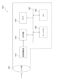
- FIG. 1 is a diagram showing an overall configuration of a solid-state imaging device according to a first embodiment.
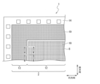
- FIG. 2 is a diagram showing a planar configuration of one of the four corners of a pixel area.
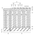
- 3 is a diagram showing a cross-sectional configuration of the solid-state imaging device taken along line AA in FIG. 2.
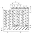
- 3 is a diagram showing a cross-sectional configuration of the solid-state imaging device taken along line BB in FIG. 2.
- 1A to 1C are diagrams illustrating a method for manufacturing a solid-state imaging device.
- 1A to 1C are diagrams illustrating a method for manufacturing a solid-state imaging device.
- 1A to 1C are diagrams illustrating a method for manufacturing a solid-state imaging device.
- FIGS. 1A to 1C are diagrams illustrating a method for manufacturing a solid-state imaging device.
- 1A to 1C are diagrams illustrating a method for manufacturing a solid-state imaging device.
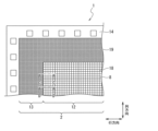
- 13 is a diagram showing a planar configuration of one of the four corners of a pixel region 2 of a solid-state imaging device according to a second embodiment.
- FIG. 11 is a diagram showing a cross-sectional configuration of a solid-state imaging device according to a second embodiment when cut along line CC in FIG. 10.
- 11 is a diagram showing a cross-sectional configuration of a solid-state imaging device according to a second embodiment when cut along line DD in FIG. 10.
- FIG. 3 is a diagram showing a cross-sectional configuration of a solid-state imaging device according to a third embodiment when cut along line AA in FIG. 2.
- 3 is a diagram showing a cross-sectional configuration of a solid-state imaging device according to a third embodiment when cut along line BB in FIG. 2.
- FIG. 13 is a diagram showing a schematic configuration of an electronic device according to a fourth embodiment.
- FIG. 1 is a diagram illustrating an example of a schematic configuration of an endoscope system. 17 is a block diagram showing an example of the functional configuration of the camera and the CCU shown in FIG. 16.
- FIG. 1 is a diagram illustrating an example of a schematic configuration of a microsurgery system.
- FIGS. 1 to 18 An example of a light detection device and electronic device according to an embodiment of the present disclosure will be described with reference to FIGS. 1 to 18.
- the embodiments of the present disclosure will be described in the following order. Note that the present disclosure is not limited to the following examples.
- the effects described in this specification are illustrative and not limiting, and other effects may also be present.
- First embodiment solid-state imaging device 1-1 Overall configuration of solid-state imaging device 1-2 Configuration of main parts 1-3 Manufacturing method of solid-state imaging device 2.
- Second embodiment solid-state imaging device 2-1 Configuration of main parts 3.
- Third embodiment solid-state imaging device 3-1 Configuration of main parts 3-2 Modification 4.
- Fourth embodiment Application to electronic devices 5.
- Fifth embodiment Application to moving objects
- FIG. 1 is a diagram showing an overall configuration of the solid-state imaging device 1 according to the first embodiment.
- the solid-state imaging device 1 in Fig. 1 is a back-illuminated CMOS (Complementary Metal Oxide Semiconductor) image sensor. As shown in Fig.
- CMOS Complementary Metal Oxide Semiconductor
- the solid-state imaging device 1 captures image light (incident light) from a subject via a lens group 1001, converts the amount of incident light focused on an imaging surface into an electrical signal on a pixel-by-pixel basis, and outputs the electrical signal as a pixel signal.
- the solid-state imaging device 1 includes a pixel region 2, a vertical drive circuit 3, a column signal processing circuit 4, a horizontal drive circuit 5, an output circuit 6, and a control circuit .
- the pixel region 2 has a plurality of pixels 8 arranged in a two-dimensional array.
- Each pixel 8 has a photoelectric conversion unit PD (see FIG. 3) and a plurality of pixel transistors (e.g., a transfer transistor, a reset transistor, an amplification transistor, and a selection transistor).
- the pixel region 2 includes an effective pixel region 12 and a light-shielded pixel region 13 located around the effective pixel region 12.
- the light-shielded pixel region 13 has, as light-shielded pixels, OPB (Optical Black) pixels and dummy pixels for obtaining a reference signal of an optical black level.
- OPB Optical Black
- the vertical drive circuit 3 is configured, for example, by a shift register, and sequentially selects each pixel 8 in the pixel region 2 on a row-by-row basis by, for example, sequentially outputting selection pulses to pixel drive wiring 9, and outputs pixel signals of the selected pixels 8 to the column signal processing circuit 4 through vertical signal lines 10.
- An example of the pixel signal is a signal obtained from charges (e.g., electrons) generated in the photoelectric conversion unit PD.
- the column signal processing circuit 4 is arranged, for example, for each column of pixels 8, and performs signal processing such as noise removal for each pixel column on signals output from one row of pixels 8. For example, correlated double sampling (CDS) for removing fixed pattern noise specific to each pixel and AD (Analog-to-Digital) conversion can be used as the signal processing.
- the horizontal drive circuit 5 is, for example, composed of a shift register, and sequentially outputs horizontal scanning pulses to the column signal processing circuits 4, selects the column signal processing circuits 4 in order, and causes the selected column signal processing circuit 4 to output pixel signals that have been subjected to signal processing to the horizontal signal line 11.
- the output circuit 6 performs signal processing on the pixel signals sequentially output from each of the column signal processing circuits 4 through the horizontal signal line 11, and outputs the signal.
- various types of digital signal processing such as buffering, black level adjustment, column variation correction, etc.
- black level adjustment for example, a process of correcting the black level of the pixel signal to "0" by subtracting a reference signal of an optical black level obtained from the pixel 8 (OPB pixel) in the light-shielded pixel region 13 from the pixel signal obtained from the pixel 8 (effective pixel) in the effective pixel region 12 can be adopted.
- the control circuit 7 generates clock signals and control signals that serve as a reference for the operation of the vertical drive circuit 3, the column signal processing circuit 4, the horizontal drive circuit 5, etc., based on a vertical synchronization signal, a horizontal synchronization signal, and a master clock signal (not shown). Then, the control circuit 7 outputs the generated clock signals and control signals to the vertical drive circuit 3, the column signal processing circuit 4, the horizontal drive circuit 5, etc.
- FIG. 2 is a diagram showing a planar configuration of one of the four corners of the pixel region 2.
- FIG. 2 the structure above the light-shielding metals 18, 19 is omitted so that the light-shielding metals 18, 19 can be clearly seen.
- FIG. 3 is a diagram showing a cross-sectional configuration of the solid-state imaging device 1 when cut along line A-A in FIG. 2.
- FIG. 3 illustrates a case where pupil correction is performed to shift the position of the light-shielding metal 18 toward the center of the pixel region 2 (the lower side in FIG. 3), and the photoelectric conversion unit PD is located below the light-shielding metal 18.
- FIG. 3 illustrates a case where pupil correction is performed to shift the position of the light-shielding metal 18 toward the center of the pixel region 2 (the lower side in FIG. 3), and the photoelectric conversion unit PD is located below the light-shielding metal 18.
- the pixel region 2 has an effective pixel region 12 located in the center of the pixel region 2 and a light-shielding pixel region 13 surrounding the effective pixel region 12 .
- the effective pixel region 12 is a region where a subject is imaged. As shown in FIG.
- the solid-state imaging device 1 has a semiconductor substrate 14, and an insulator 15, a first conductor 16, an insulating film 17, and a light-shielding metal 18 are laminated in this order on the light-receiving surface (hereinafter also referred to as the "back surface S1" or in a broader sense as the "first surface") of the semiconductor substrate 14.
- the back surface S1 the light-receiving surface
- the back surface S2 the light-receiving surface
- a color filter, an on-chip lens, or the like may be formed thereon.
- a wiring layer 20 is disposed on the surface (hereinafter also referred to as the "front surface S3" or in a broader sense as the "second surface") of the semiconductor substrate 14 opposite to the back surface S1.
- the light-shielding pixel region 13 is a region surrounding the periphery of the effective pixel region 12.
- the solid-state imaging device 1 has a semiconductor substrate 14 shared with the effective pixel region 12, and a light-shielding metal 19 is disposed on a back surface S1 of the semiconductor substrate 14.
- a wiring layer 20 is disposed on a front surface S3 of the semiconductor substrate 14.
- the semiconductor substrate 14 is a substrate made of, for example, silicon (Si).
- the semiconductor substrate 14 is shared by the effective pixel region 12 and the light-shielding pixel region 13, and a photoelectric conversion unit PD is formed in each region corresponding to each pixel 8. That is, a plurality of photoelectric conversion units PD are formed in a two-dimensional array on the semiconductor substrate 14.
- the photoelectric conversion unit PD forms a photodiode by a pn junction of a p-type semiconductor region and an n-type semiconductor region, and photoelectrically converts incident light to generate electric charges. The generated electric charges are stored in an electrostatic capacitance generated by the pn junction.
- an inter-pixel isolation structure 21 is formed in a region between the photoelectric conversion units PD. That is, the inter-pixel isolation structure 21 is formed in a lattice shape so as to surround each photoelectric conversion unit PD.
- the inter-pixel isolation structure 21 has a first inter-pixel isolation structure 22 which is a part in the effective pixel region 12, and a second inter-pixel isolation structure 23 which is a part in the light-shielding pixel region 13.
- the first inter-pixel isolation structure 22 is formed from the back surface S1 of the semiconductor substrate 14 to a partway between the back surface S1 and the front surface S3.
- a first conductor 16 is arranged from the back surface S1 to a partway between the back surface S1 and the front surface S3.
- the first inter-pixel isolation structure 22 has a trench portion 24, and an insulator 15 and a first conductor 16 arranged in the trench portion 24.
- the trench portion 24 is formed from the back surface S1 of the semiconductor substrate 14 to partway between the back surface S1 and the front surface S3, and its sidewall surface and bottom surface form the outline of the first inter-pixel isolation structure 22.
- the insulator 15 continuously covers the sidewall surface of the trench portion 24 and the back surface S1 of the semiconductor substrate 14 in the effective pixel region 12.
- the formation range of the insulator 15 on the back surface S1 side of the semiconductor substrate 14 is up to the boundary between the effective pixel region 12 and the light-shielding pixel region 13 so that the insulator 15 does not cover the back surface S1 of the light-shielding pixel region 13.
- the material (insulating material) of the insulator 15 can be, for example, silicon oxide (SiO).
- the first conductor 16 is embedded in the space in the trench portion 24, that is, in the space between the sidewall surfaces covered with the insulator 15. As a result, each part of the first conductor 16 in the trench portion 24 is electrically integrated.
- the first conductor 16 is disposed from the back surface S1 of the semiconductor substrate 14 to the bottom surface of the trench portion 24.
- the first conductor 16 also covers the space in the trench portion 24, as well as the region (lattice region) along the photoelectric conversion units PD on the light receiving surface (hereinafter also referred to as the "back surface S6" of the insulator 15 located on the back surface S1 of the semiconductor substrate 14.
- the first conductor 16 is disposed continuously in the first inter-pixel separation structure 22 and in the region along the photoelectric conversion units PD on the back surface S1 of the semiconductor substrate 14 in the effective pixel region 12.
- the formation range of the first conductor 16 on the back surface S6 side of the insulator 15 is up to the boundary between the effective pixel region 12 and the light-shielding pixel region 13 so as not to reach the light-shielding pixel region 13.
- a conductive material can be used as the material of the first conductor 16.
- ITO Indium Tin Oxide
- STI 50 is formed in a lattice shape along the first inter-pixel isolation structure 22.
- the second pixel isolation structure 23 is formed so as to penetrate the semiconductor substrate 14 from the back surface S1 to the front surface S3 of the semiconductor substrate 14.
- a conductor (hereinafter also referred to as a "second conductor 25") is disposed in the second pixel isolation structure from the back surface S1 to the front surface S3.
- the second pixel isolation structure 23 has a trench portion 26, and an insulator 27 and a second conductor 25 disposed in the trench portion 26.
- the trench portion 26 penetrates the semiconductor substrate 14 from the back surface S1 to the front surface S3 of the semiconductor substrate 14, and the sidewall surface forms the outer shape of the second pixel isolation structure 23.
- the insulator 27 continuously covers the sidewall surface of the trench portion 26.
- silicon oxide can be used as the material of the insulator 27.
- the second conductor 25 is embedded in the space in the trench portion 26, that is, the space between the sidewall surfaces covered with the insulator 27. As a result, each part of the second conductor 25 in the trench portion 26 is electrically integrated.
- the space between the sidewall surfaces covered with the insulator 27 (that is, the space in the second pixel isolation structure 23) and the space between the insulators 15 in the first pixel isolation structure 22 are connected to each other, and the second conductor 25 and the first conductor 16 are electrically connected by contacting each other at their ends.
- the second conductor 25 is disposed so as to penetrate the semiconductor substrate 14 from the back surface S1 to the front surface S3 of the semiconductor substrate 14.
- the second conductor 25 is exposed on each of the front surface S3 and the back surface S1 of the semiconductor substrate 14.
- a conductive material can be used as the material of the second conductor 25.
- doped polysilicon doped with boron (B) or the like can be used. That is, in the first embodiment, the first conductor 16 and the second conductor 25 are formed using different conductive materials. More specifically, the first conductor 16 is formed using a conductive material having a lower light absorption rate than the second conductor 25.
- the relationship between the light absorption rate of ITO and the light absorption rate of doped polysilicon is light absorption rate of ITO ⁇ light absorption rate of doped polysilicon.
- the second conductor 25 is electrically connected to a negative bias voltage supply source on the surface S3 side, and a negative bias voltage is applied from the surface S3 side.
- a negative bias voltage is applied from the surface S3 side.
- the peripheral portion of the second inter-pixel separation structure 23 can be made to have a high hole concentration in the light-shielded pixel region 13, and the generation of dark current can be suppressed.
- a contact 28 formed on a portion of the second conductor 25 on the surface S3 side is connected to the second conductor 25, and the second conductor 25 is connected to the negative bias voltage supply source via the contact 28.
- the insulating film 17 is formed so as to continuously cover the light receiving surface of the first conductor 16 (hereinafter also referred to as "rear surface S4") and the portion of the rear surface S6 of the insulator 15 where the first conductor 16 is not present.
- the light-shielding metal 18 is disposed on the light-receiving surface (hereinafter also referred to as "rear surface S5") of the insulating film 17 in the effective pixel region 12, and is formed so as to cover the region along the photoelectric conversion unit PD on the rear surface S5 of the insulating film 17 in the effective pixel region 12.
- the light-shielding metal 19 is disposed on the rear surface S1 of the semiconductor substrate 14 in the light-shielding pixel region 13, and is formed so as to cover the entire rear surface S1 of the semiconductor substrate 14 in the light-shielding pixel region 13.
- the opposing surface (hereinafter also referred to as "front surface S7") of the light-shielding metal 19 facing the rear surface S1 of the semiconductor substrate 14 is in contact with and electrically connected to the second conductor 25 (i.e., the end of the second conductor 25 on the rear surface S1 side) exposed on the rear surface S1 of the semiconductor substrate 14.
- the end of the light-shielding metal 19 on the effective pixel region 12 side is in contact with and electrically connected to the end of the part of the first conductor 16 located on the rear surface S1 on the light-shielding pixel region 13 side.
- the first conductor 16 and the second conductor 25 are electrically connected to each other via the light-shielding metal 19.
- the negative bias voltage applied to the second conductor 25 from the surface S3 side is applied to the first conductor 16 via the second conductor 25 and the light-shielding metal 19. That is, a transmission path for the negative bias voltage is formed using the light-shielding metal 19 used for shading the photoelectric conversion unit PD in the light-shielding pixel region 13. Therefore, in the effective pixel region 12, the periphery of the first pixel separation structure 22 can be made into a high hole concentration state, and the generation of dark current can be suppressed.
- tungsten (W), aluminum (Al), and copper (Cu) can be adopted as the material of the light-shielding metals 18 and 19.
- the light-shielding metals 18 and 19 are separated at the boundary between the effective pixel region 12 and the light-shielding pixel region 13 and are not electrically connected.
- the wiring layer 20 has an interlayer insulating film and wiring (not shown) stacked in multiple layers with the interlayer insulating film interposed therebetween, and drives the pixel transistors (not shown) of each pixel 8 via the multiple layers of wiring.
- the solid-state imaging device 1 having the above configuration, light is incident from the rear surface S1 side of the semiconductor substrate 14, the incident light is transmitted through an on-chip lens and a color filter (not shown), and the transmitted light is photoelectrically converted in the photoelectric conversion unit PD to generate electric charges. The generated electric charges are then output as pixel signals from vertical signal lines 10 (see FIG. 1 ) formed by wiring in the wiring layer 20. Furthermore, in the solid-state imaging device 1 according to the first embodiment, an end portion on the surface S3 side of the second conductor 25 in the second inter-pixel isolation structure 23 in the light-shielding pixel region 13 is electrically connected to a supply source of a negative bias voltage.
- a negative bias voltage is applied to the first conductor 16 in the first inter-pixel isolation structure 22 in the effective pixel region 12 via the second conductor 25 and the light-shielding metal 19, and the peripheral portion of the first inter-pixel isolation structure 22 is brought into a high hole concentration state, suppressing the generation of dark current.
- the first conductor 16 in the first inter-pixel isolation structure 22 in the effective pixel region 12 and the second conductor 25 in the second inter-pixel isolation structure 23 in the light-shielding pixel region 13 are formed using different conductive materials. Therefore, by selecting a conductive material according to desired pixel characteristics as the conductive material of the first conductor 16 in the first inter-pixel isolation structure 22 in the effective pixel region 12, the characteristics of the pixel 8 can be improved. More specifically, in the first embodiment, the first conductor 16 is formed using a conductive material (ITO) having a lower light absorption rate than the second conductor 25.
- ITO conductive material
- the second conductor 25 is made of doped polysilicon.
- doped polysilicon has better embedding properties than ITO. Therefore, during the manufacture of the solid-state imaging device 1, the process of embedding the second conductor 25 in the space within the trench portion 26 of the second inter-pixel isolation structure 23, i.e., the narrow space penetrating the semiconductor substrate 14, can be performed relatively easily.
- a method for manufacturing the solid-state imaging device 1 according to the first embodiment will be described.
- a semiconductor substrate 14 on which a second pixel isolation structure 23 and a wiring layer 20 are formed is prepared.
- Doped polysilicon is embedded as a second conductor 25 in the second pixel isolation structure 23.
- a trench portion 24 of the first pixel isolation structure 22 is formed on the rear surface S1 of the prepared semiconductor substrate 14 using lithography and dry etching.
- an insulator 27 is formed so as to continuously cover the sidewall surface of the formed trench portion 24 and the rear surface S1 of the semiconductor substrate 14. For example, chemical vapor deposition (CVD) or thermal oxidation can be used as a method for forming the insulator 27.
- CVD chemical vapor deposition
- thermal oxidation can be used as a method for forming the insulator 27.
- the first conductor 16 is formed so as to continuously cover the space between the sidewall surfaces covered with the insulator 15 and the back surface S6 of the insulator 27.
- ITO which has a lower light absorption rate than doped polysilicon, is used as the material of the first conductor 16.
- an insulating film 17 is formed on the back surface S4 of the first conductor 16, and then a resist mask 29 having an opening at a position where the light-shielding metal 19 (see FIG. 3) is to be formed is formed.
- etching is performed through the resist mask 29 to remove a part of the first conductor 16 and the insulator 15 to expose the back surface S1 of the semiconductor substrate 14.
- the resist mask 29 is removed, and as shown in FIG. 9, a film of a constant thickness is formed using the material of the light-shielding metal 19 (for example, tungsten (W)) on the entire back surface S1 side of the semiconductor substrate 14.
- the material of the light-shielding metal 19 for example, tungsten (W)
- the surface S7 of the light-shielding metal 19 is electrically connected to the second conductor 25, and the end of the light-shielding metal 19 on the effective pixel region 12 side is electrically connected to the first conductor 16.
- a contact 28 connected to a supply source of a negative bias voltage is connected to the first conductor 16 via the second conductor 25 and the light-shielding metal 19.
- the material of the light-shielding metal 19 that has been formed is removed from the back surface S5 of the insulating film 17 in the effective pixel region 12 to form the light-shielding metal 19.
- the light-shielding metal 18 (see FIG. 3), a color filter, an on-chip lens, and the like are formed on the back surface S5 of the insulating film 17 in the effective pixel region 12.
- the solid-state imaging device 1 shown in FIG. 3 is manufactured.
- FIG. 10 is a diagram corresponding to FIG. 2 of the first embodiment, and is a diagram showing a planar configuration of one of the four corners of the pixel region 2 of the solid-state imaging device 1 according to the second embodiment.
- FIG. 11 is a diagram corresponding to FIG. 3 of the first embodiment, and is a diagram showing a cross-sectional configuration of the solid-state imaging device 1 when broken along line CC in FIG. 10.
- FIG. 12 is a diagram corresponding to FIG.
- FIG. 4 of the first embodiment is a diagram showing a cross-sectional configuration of the solid-state imaging device 1 when broken along line D-D in FIG. 10.
- the solid-state imaging device 1 according to the second embodiment is different from the solid-state imaging device 1 according to the first embodiment in the configurations and materials of the first conductor 16 and the second conductor 25, and the configuration of the light-shielding metal 18.
- the insulating film 17 is omitted.
- the first conductor 16 is disposed in the space within the trench portion 24, i.e., in the space between the sidewall surfaces covered with the insulator 15, from the back surface S1 to the bottom surface of the trench portion 24.
- the first conductors 16 in each portion within the trench portion 24 are electrically integrated, and the back surface S1 side of the first conductor 16 is exposed to the back surface S1 of the semiconductor substrate 14.
- the material (conductive material) of the first conductor 16 for example, doped polysilicon can be used.
- the second conductor 25 is embedded in the space in the trench portion 26, that is, in the space between the sidewall surfaces covered with the insulator 27. As a result, each portion of the second conductor 25 in the trench portion 26 is electrically integrated.
- the second conductor 25 is disposed so as to penetrate the semiconductor substrate 14 from the back surface S1 to the front surface S3 of the semiconductor substrate 14. By penetrating the semiconductor substrate 14, the second conductor 25 is exposed on each of the front surface S3 and the back surface S1 of the semiconductor substrate 14.
- the material (conductive material) of the second conductor 25 can be the same material as the light-shielding metal 19, and for example, tungsten (W) can be adopted. That is, in the second embodiment, the first conductor 16 is formed of a conductive material having a higher light absorption rate than the second conductor 25.
- the light absorption rate of doped polysilicon and the light absorption rate of tungsten (W) have a relationship such that the light absorption rate of doped polysilicon is greater than the light absorption rate of tungsten (W).
- the second conductor 25 has a surface S3 side electrically connected to a negative bias voltage source via a contact 28, and a negative bias voltage is applied from the surface S3 side. By applying a negative bias voltage, in the light-shielded pixel region 13, the peripheral portion of the second inter-pixel separation structure 23 can be brought into a high hole concentration state, and the generation of dark current can be suppressed.
- the light-shielding metal 18 is disposed on the back surface S6 side of the insulator 15 in the effective pixel region 12, and is formed so as to cover the region along the back surface S6 between the photoelectric conversion units PD of the insulator 15 in the effective pixel region 12.
- the surface of the light-shielding metal 18 facing the insulator 15 (hereinafter also referred to as the "front surface S8") has a convex portion 30 penetrating the insulator 15 at a portion facing the first conductor 16, and is in contact with and electrically connected to the first conductor 16 (i.e., the end of the first conductor 16 on the back surface S1 side) exposed on the back surface S1 of the semiconductor substrate 14.
- the light-shielding metal 19 is disposed on the back surface S1 side of the semiconductor substrate 14 in the light-shielding pixel region 13, and is formed so as to cover the entire back surface S1 of the semiconductor substrate 14 in the light-shielding pixel region 13.
- the front surface S7 of the light-shielding metal 19 is in contact with and electrically connected to the second conductor 25 (i.e., the end of the second conductor 25 on the back surface S1 side) exposed on the back surface S1 of the semiconductor substrate 14.
- the first conductor 16 and the second conductor 25 are electrically connected to each other via the light-shielding metals 18 and 19 .
- the negative bias voltage applied to the second conductor 25 from the surface S3 side is applied to the first conductor 16 via the second conductor 25 and the light-shielding metals 18 and 19. That is, a transmission path of the negative bias voltage is formed using the light-shielding metal 19 and the light-shielding metal 18 used for shading the photoelectric conversion unit PD in the light-shielding pixel region 13. Therefore, in the effective pixel region 12, the peripheral portion of the first pixel separation structure 22 can be made into a high hole concentration state, and the generation of dark current can be suppressed.
- tungsten (W), aluminum (Al), and copper (Cu) can be used as the material of the light-shielding metals 18 and 19.
- FIG 11 illustrates a case where the light-shielding metals 18 and 19 and the second conductor 25 are integrally formed using the same material.
- the light-shielding metals 18 and 19 are connected at the boundary between the effective pixel region 12 and the light-shielding pixel region 13 and integrally formed.
- the first conductor 16 in the first inter-pixel isolation structure 22 in the effective pixel region 12 and the second conductor 25 in the second inter-pixel isolation structure 23 in the light-shielding pixel region 13 are formed using different conductive materials. Therefore, by selecting a conductive material according to the desired pixel characteristics as the conductive material of the first conductor 16 in the first inter-pixel isolation structure 22 in the effective pixel region 12, the characteristics of the pixel 8 can be improved. More specifically, in the second embodiment, the first conductor 16 is formed from a conductive material (doped polysilicon) having a higher light absorption rate than the second conductor 25.
- the absorption of incident light by the first inter-pixel isolation structure 22 can be improved, and optical color mixing can be more appropriately suppressed. For this reason, it is preferable in a configuration where color mixing is more of a problem than sensitivity, such as when a SPAD (Single Photon Avalanche Diode), in which avalanche multiplication occurs in response to incident photons and current flows, is used as the photoelectric conversion unit PD.
- SPAD Single Photon Avalanche Diode
- FIG. 13 is a diagram corresponding to FIG. 3 of the first embodiment, and is a diagram showing a cross-sectional configuration of the solid-state imaging device 1 when cut along line A-A in FIG. 2.
- FIG. 14 is a diagram corresponding to FIG. 4 of the first embodiment, and is a diagram showing a cross-sectional configuration of the solid-state imaging device 1 when cut along line B-B in FIG. 2.
- FIG. 13 and FIG. 14 the parts corresponding to FIG. 3 and FIG.
- the solid-state imaging device 1 according to the third embodiment differs from the solid-state imaging device 1 according to the first embodiment in the configuration of the insulator 15 and the materials and configurations of the first conductor 16 and the second conductor 25.
- the insulator 15 continuously covers the sidewall surfaces of the trench portions 24 in the effective pixel region 12 and the entire back surface S1 of the semiconductor substrate 14 (both the effective pixel region 12 and the light-shielded pixel region 13).
- the first conductor 16 is disposed in the space in the trench portion 24, that is, in the space between the sidewall surfaces covered with the insulator 15, from the back surface S1 to the bottom surface of the trench portion 24.
- each portion of the first conductor 16 in the trench portion 24 is electrically integrated.
- the first conductor 16 continuously covers a region (lattice region) along the photoelectric conversion units PD on the back surface S6 of the insulator 15 in the effective pixel region 12, and the entire back surface S6 of the insulator 15 in the light-shielded pixel region 13. That is, the first conductor 16 is continuously disposed in the first inter-pixel isolation structure 22, a region along the photoelectric conversion units PD on the back surface S1 of the semiconductor substrate 14 in the effective pixel region 12, and the entire back surface S1 of the semiconductor substrate 14 in the light-shielded pixel region 13.
- the surface of the first conductor 16 facing the insulator 15 (hereinafter also referred to as "surface S9") has a protrusion 31 penetrating the insulator 15 at a portion facing the second conductor 25, and is in contact with the rear surface S1 of the semiconductor substrate 14.
- the material (conductive material) of the first conductor 16 for example, ITO can be used.
- the second conductor 25 is embedded in the space in the trench portion 26, that is, in the space between the sidewall surfaces covered with the insulator 27. As a result, each part of the second conductor 25 in the trench portion 26 is electrically integrated.
- the second conductor 25 is arranged so as to penetrate the semiconductor substrate 14 from the back surface S1 to the front surface S3 of the semiconductor substrate 14. By penetrating the semiconductor substrate 14, the second conductor 25 is exposed on each of the front surface S3 and the back surface S1 of the semiconductor substrate 14.
- the end of the second conductor 25 exposed from the front surface S3 side is electrically connected to a negative bias voltage supply source via the contact 28, and a negative bias voltage is applied from the front surface S3 side.
- a negative bias voltage By applying a negative bias voltage, the peripheral part of the second inter-pixel separation structure 23 can be made into a high hole concentration state in the light-shielded pixel region 13, and the generation of dark current can be suppressed.
- the end of the second conductor 25 exposed from the back surface S1 side is in contact with and electrically connected to the first conductor 16 located on the back surface S1 side of the semiconductor substrate 14 in the light-shielding pixel region 13.
- the first conductor 16 and the second conductor 25 are electrically connected to each other without passing through the light-shielding metals 18 and 19. Therefore, the negative bias voltage applied to the second conductor 25 from the front surface S3 side is applied to the first conductor 16 in the first pixel isolation structure 22 via the second conductor 25 and the first conductor 16 located on the back surface S1 side.
- a transmission path of the negative bias voltage to the first conductor 16 in the first pixel isolation structure 22 is formed using the first conductor 16 located on the back surface S1 side. Therefore, in the effective pixel region 12, the peripheral portion of the first pixel isolation structure 22 can be made to have a high hole concentration, and the generation of dark current can be suppressed.
- tungsten (W) can be used as the material (conductive material) of the second conductor 25. That is, in the third embodiment, the first conductor 16 is formed of a conductive material with a lower light absorption rate than the second conductor 25.
- the light absorption rate of ITO and the light absorption rate of tungsten (W) have the following relationship: light absorption rate of ITO ⁇ light absorption rate of tungsten.
- the first conductor 16 in the first inter-pixel isolation structure 22 in the effective pixel region 12 and the second conductor 25 in the second inter-pixel isolation structure 23 in the light-shielding pixel region 13 are formed using different conductive materials. Therefore, by selecting a conductive material according to desired pixel characteristics as the conductive material of the first conductor 16 in the first inter-pixel isolation structure 22 in the effective pixel region 12, the characteristics of the pixel 8 can be improved. More specifically, in the third embodiment, the first conductor 16 is formed using a conductive material (ITO) having a lower light absorption rate than the second conductor 25.
- ITO conductive material
- the absorption of incident light by the first inter-pixel isolation structure 22 can be suppressed, and the sensitivity can be improved.
- the first conductor 16 located on the back surface S1 side of the semiconductor substrate 14 in the light-shielded pixel region 13 is configured to be used as a transmission path for a negative bias voltage. Therefore, compared to the case where the light-shielding metal 19 is used as the transmission path, for example, it is not necessary to prepare a material for forming the transmission path separately from the material for the first conductor 16, and an increase in the number of steps associated with the formation of the transmission path can be suppressed.
- this technology can be applied to light detection devices in general, including distance measuring sensors that measure distance, also known as ToF (Time of Flight) sensors, in addition to the solid-state imaging device 1 as the image sensor described above.
- a distance measuring sensor is a sensor that emits light toward an object, detects the reflected light that is reflected back from the surface of the object, and calculates the distance to the object based on the flight time from when the light is emitted to when the reflected light is received.
- the structure of pixel 8 described above can be adopted as the light receiving pixel structure of this distance measuring sensor.
- FIG. 15 is a diagram showing an example of a schematic configuration of an imaging device (such as a video camera or a digital still camera) as an electronic device to which the present technology is applied.
- the imaging device 1000 includes a lens group 1001, a solid-state imaging device 1002 (solid-state imaging device 1 according to the first embodiment), a DSP (Digital Signal Processor) circuit 1003, a frame memory 1004, a monitor 1005, and a memory 1006.
- the DSP circuit 1003, the frame memory 1004, the monitor 1005, and the memory 1006 are connected to each other via a bus line 1007.
- the lens group 1001 guides incident light (image light) from a subject to the solid-state imaging device 1002 , and forms an image on the light receiving surface (pixel region) of the solid-state imaging device 1002 .
- the solid-state imaging device 1002 is made up of the CMOS image sensor according to the first embodiment described above.
- the solid-state imaging device 1002 converts the amount of incident light focused on the light receiving surface by the lens group 1001 into an electrical signal on a pixel-by-pixel basis and supplies the signal to the DSP circuit 1003 as a pixel signal.
- the DSP circuit 1003 performs predetermined image processing on the pixel signals supplied from the solid-state imaging device 1002.
- the DSP circuit 1003 supplies the image signals after the image processing to a frame memory 1004 on a frame-by-frame basis, and causes the image signals to be temporarily stored in the frame memory 1004.
- the monitor 1005 is formed of a panel-type display device such as a liquid crystal panel, an organic EL (Electro Luminescence) panel, etc.
- the monitor 1005 displays an image (moving image) of a subject based on pixel signals in frame units temporarily stored in the frame memory 1004.
- the memory 1006 is composed of a DVD, a flash memory, etc.
- the memory 1006 reads out and records the pixel signals temporarily stored in the frame memory 1004 on a frame-by-frame basis.
- the electronic device to which the solid-state imaging device 1 can be applied is not limited to the imaging device 1000, but can also be applied to other electronic devices.
- the solid-state imaging device 1 according to the first embodiment is used as the solid-state imaging device 1002, other configurations can also be adopted.
- the solid-state imaging device 1 according to the second or third embodiment, the solid-state imaging device 1 according to a modified example, or another light detection device to which the present technology is applied can be used.
- the technology according to the present disclosure can be applied to a medical imaging system.
- the medical imaging system is a medical system that uses imaging technology, such as an endoscope system or a microscope system.
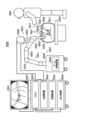
- FIG. 16 is a diagram showing an example of a schematic configuration of an endoscope system 5000 to which the technology according to the present disclosure can be applied.
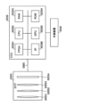
- Fig. 17 is a diagram showing an example of a configuration of an endoscope 5001 and a CCU (Camera Control Unit) 5039.
- Fig. 16 shows a state in which an operator (e.g., a doctor) 5067 who is a participant in the operation is performing an operation on a patient 5071 on a patient bed 5069 using the endoscope system 5000. As shown in Fig.
- the endoscope system 5000 is composed of an endoscope 5001 which is a medical imaging device, a CCU 5039, a light source device 5043, a recording device 5053, an output device 5055, and a support device 5027 that supports the endoscope 5001.
- an insertion aid called a trocar 5025 is inserted into the patient 5071. Then, a scope 5003 and surgical tools 5021 connected to an endoscope 5001 are inserted into the body of the patient 5071 via the trocar 5025. Examples of the surgical tools 5021 include energy devices such as an electric scalpel, and forceps.
- a surgical image which is a medical image showing the inside of the body of a patient 5071 captured by an endoscope 5001, is displayed on a display device 5041.
- a surgeon 5067 performs treatment on the surgical subject using a surgical tool 5021 while viewing the surgical image displayed on the display device 5041.
- the medical image is not limited to a surgical image, and may be a diagnostic image captured during a diagnosis.
- the endoscope 5001 is an imaging unit that images the inside of the patient 5071, and is, for example, a camera 5005 including a focusing optical system 50051 that focuses incident light, a zoom optical system 50052 that changes the focal length of the imaging unit to enable optical zoom, a focus optical system 50053 that changes the focal length of the imaging unit to enable focus adjustment, and a light receiving element 50054, as shown in FIG. 17.
- the endoscope 5001 generates a pixel signal by focusing light on the light receiving element 50054 via the connected scope 5003, and outputs the pixel signal to the CCU 5039 through a transmission system.
- the scope 5003 has an objective lens at its tip and is an insertion part that guides light from the connected light source device 5043 into the body of the patient 5071.
- the scope 5003 is, for example, a rigid scope in the case of a rigid endoscope, or a flexible scope in the case of a flexible endoscope.
- the scope 5003 may be a direct endoscope or an oblique endoscope.
- the pixel signal may be a signal based on a signal output from a pixel, for example, a RAW signal or an image signal.
- a memory may be mounted on the transmission system connecting the endoscope 5001 and the CCU 5039, and parameters related to the endoscope 5001 and the CCU 5039 may be stored in the memory.
- the memory may be disposed, for example, on a connection part or a cable of the transmission system.
- the parameters at the time of shipment of the endoscope 5001 and the parameters changed when the power is applied may be stored in the memory of the transmission system, and the operation of the endoscope may be changed based on the parameters read from the memory.
- the endoscope and the transmission system may be referred to as a set as an endoscope.
- the light receiving element 50054 is a sensor that converts the received light into a pixel signal, and is, for example, a CMOS (Complementary Metal Oxide Semiconductor) type imaging element. It is preferable that the light receiving element 50054 is an imaging element capable of color photography having a Bayer array.
- CMOS Complementary Metal Oxide Semiconductor
- the light receiving element 50054 is preferably an imaging element having a number of pixels corresponding to a resolution of, for example, 4K (3840 horizontal pixels x 2160 vertical pixels), 8K (7680 horizontal pixels x 4320 vertical pixels), or square 4K (3840 or more horizontal pixels x 3840 or more vertical pixels).
- the light receiving element 50054 may be one sensor chip or multiple sensor chips.
- a prism may be provided to separate the incident light into predetermined wavelength bands, and each wavelength band may be imaged by a different light receiving element.
- multiple light receiving elements may be provided for stereoscopic vision.
- the light receiving element 50054 may be a sensor including an arithmetic processing circuit for image processing in a chip structure, or may be a ToF (Time of Flight) sensor.
- the transmission system may be, for example, an optical fiber cable or wireless transmission.
- the wireless transmission may be performed by any method as long as the pixel signal generated by the endoscope 5001 can be transmitted.
- the endoscope 5001 and the CCU 5039 may be connected wirelessly, or the endoscope 5001 and the CCU 5039 may be connected via a base station in the operating room.
- the endoscope 5001 may simultaneously transmit not only the pixel signal but also information related to the pixel signal (for example, the processing priority of the pixel signal, a synchronization signal, etc.).
- the endoscope may be configured such that the scope and the camera are integrated, or a light receiving element is provided at the tip of the scope.
- the CCU 5039 is a control device that comprehensively controls the connected endoscope 5001 and the light source device 5043.
- the CCU 5039 is an information storage device having an FPGA 50391, a CPU 50392, a RAM 50393, a ROM 50394, a GPU 50395, and an I/F 50396.
- the CCU 5039 may also comprehensively control the connected display device 5041, recording device 5053, and output device 5055.
- the CCU 5039 may control the irradiation timing, irradiation intensity, and irradiation
- the CCU 5039 controls the type of light source.
- the CCU 5039 performs image processing such as development processing (e.g., demosaic processing) and correction processing on the pixel signals output from the endoscope 5001, and transmits the processed images to an external device such as a display device 5041.
- the resulting pixel signal (eg, an image) is output.
- the CCU 5039 transmits a control signal to the endoscope 5001 to control the driving of the endoscope 5001.
- the control signal is information on imaging conditions such as the magnification and focal length of the imaging unit, for example.
- the CCU 5039 may have an image down-conversion function and be configured to be able to simultaneously output a high-resolution (e.g., 4K) image to the display device 5041 and a low-resolution (e.g., HD) image to the recording device 5053.
- a high-resolution e.g., 4K
- a low-resolution e.g., HD
- the CCU 5039 may also be connected to an external device (e.g., a recording device, a display device, an output device, a support device) via an IP converter that converts signals into a predetermined communication protocol (e.g., IP (Internet Protocol)).
- IP Internet Protocol
- the connection between the IP converter and the external device may be configured as a wired network, or a part or all of the network may be constructed as a wireless network.
- the IP converter on the CCU 5039 side may have a wireless communication function, and the received video may be transmitted to an IP switcher or an output side IP converter via a wireless communication network such as a fifth generation mobile communication system (5G) or a sixth generation mobile communication system (6G).
- 5G fifth generation mobile communication system
- 6G sixth generation mobile communication system
- the light source device 5043 is a device capable of irradiating light in a predetermined wavelength band, and includes, for example, a plurality of light sources and a light source optical system that guides the light of the plurality of light sources.
- the light sources are, for example, a xenon lamp, an LED light source, or an LD light source.
- the light source device 5043 has, for example, LED light sources corresponding to each of the three primary colors R, G, and B, and emits white light by controlling the output intensity and output timing of each light source.
- the light source device 5043 may have a light source capable of irradiating special light used in special light observation, in addition to a light source that irradiates normal light used in normal light observation.
- the special light is light in a predetermined wavelength band different from normal light, which is light for normal light observation, and is, for example, near-infrared light (light with a wavelength of 760 nm or more), infrared light, blue light, or ultraviolet light.
- the normal light is, for example, white light or green light.
- narrowband light observation which is a type of special light observation, blue light and green light are alternately irradiated to utilize the wavelength dependency of light absorption in body tissue, and a predetermined tissue such as blood vessels on the surface of the mucous membrane can be photographed with high contrast.
- a fluorescent observation is performed by irradiating a drug injected into a body tissue with excitation light that excites the drug, and receiving the fluorescence emitted by the drug as a marker to obtain a fluorescent image, thereby making it easier for the surgeon to visually recognize the body tissue, etc., which is difficult for the surgeon to visually recognize under normal light.
- a drug such as indocyanine green (ICG) injected into the body tissue is irradiated with infrared light having an excitation wavelength band, and the fluorescence of the drug is received, thereby making it easier to visually recognize the structure of the body tissue and the affected area.
- ICG indocyanine green
- a drug e.g., 5-ALA
- the type of irradiation light of the light source device 5043 is set under the control of the CCU 5039.
- the CCU 5039 may have a mode in which normal light observation and special light observation are alternately performed by controlling the light source device 5043 and the endoscope 5001. At this time, it is preferable to superimpose information based on pixel signals obtained by special light observation on pixel signals obtained by normal light observation.
- the special light observation may be infrared light observation in which infrared light is irradiated to view the inside of an organ from its surface, or multispectral observation using hyperspectral spectroscopy. Photodynamic therapy may also be combined.
- the recording device 5053 is a device that records pixel signals (e.g., images) acquired from the CCU 5039, and is, for example, a recorder.
- the recording device 5053 records images acquired from the CCU 5039 in a HDD, an SSD, or an optical disk.
- the recording device 5053 may be connected to a network within the hospital and may be accessible from devices outside the operating room.
- the recording device 5053 may also have an image down-conversion function or an image up-conversion function.
- the display device 5041 is a device capable of displaying an image, such as a display monitor.
- the display device 5041 displays an image based on a pixel signal acquired from the CCU 5039.
- the display device 5041 may also function as an input device that enables gaze recognition, voice recognition, and instruction input by gestures by including a camera and a microphone.
- the output device 5055 is a device, such as a printer, that outputs information acquired from the CCU 5039.
- the output device 5055 prints, for example, a print image based on a pixel signal acquired from the CCU 5039 onto paper.
- the support device 5027 is a multi-joint arm including a base 5029 having an arm control device 5045, an arm 5031 extending from the base 5029, and a holding part 5032 attached to the tip of the arm 5031.
- the arm control device 5045 is configured by a processor such as a CPU, and controls the driving of the arm 5031 by operating according to a predetermined program.
- the support device 5027 controls the position and posture of the endoscope 5001 held by the holding part 5032, for example, by controlling parameters such as the length of each link 5035 constituting the arm 5031 and the rotation angle and torque of each joint 5033 by the arm control device 5045.
- the support device 5027 functions as an endoscope support arm that supports the endoscope 5001 during surgery. This allows the support device 5027 to take the place of a scopist, who is an assistant holding the endoscope 5001.
- the support device 5027 may also be a device that supports a microscope device 5301, which will be described later, and may also be called a medical support arm.
- the control of the support device 5027 may be an autonomous control method by the arm control device 5045, or a control method in which the arm control device 5045 controls the support device 5027 based on a user's input.
- control method may be a master-slave method in which the support device 5027 as a slave device (replica device), which is a patient cart, is controlled based on the movement of a master device (primary device), which is an operator console at the user's hand.
- the support device 5027 may also be remotely controlled from outside the operating room.
- an example of an endoscope system 5000 to which the technology disclosed herein can be applied has been described.
- the technology disclosed herein may be applied to a microscope system.
- [Microscope system] 18 is a diagram showing an example of a schematic configuration of a microsurgery system to which the technology according to the present disclosure can be applied.
- the same components as those in the endoscope system 5000 are denoted by the same reference numerals, and duplicated descriptions thereof will be omitted.
- FIG. 18 shows a schematic diagram of an operator 5067 performing surgery on a patient 5071 on a patient bed 5069 using a microsurgery system 5300.
- FIG. 18 omits the illustration of the cart 5037 from the configuration of the microsurgery system 5300, and shows a simplified illustration of a microscope device 5301 replacing the endoscope 5001.
- the microscope device 5301 in this explanation may refer to the microscope unit 5303 provided at the tip of the link 5035, or may refer to the entire configuration including the microscope unit 5303 and the support device 5027.
- a microsurgery system 5300 is used to display an image of the surgical site taken by a microscope device 5301 on a display device 5041 installed in an operating room in an enlarged scale.
- the display device 5041 is installed in a position facing the surgeon 5067, who performs various procedures on the surgical site, such as resecting the affected area, while observing the state of the surgical site using the image displayed on the display device 5041.
- Microsurgery systems are used, for example, in ophthalmic surgery and brain surgery.
- the support device 5027 may support other observation devices or other surgical tools at its tip instead of the endoscope 5001 or the microscope unit 5303.
- observation devices include forceps, a pneumoperitoneum tube for pneumoperitoneum, and an energy treatment tool for incising tissue or sealing blood vessels by cauterization.
- the technology disclosed herein can be suitably applied to the light receiving element of the configurations described above.
- the technology disclosed herein can be applied to the light receiving element, clearer images of the surgical site can be obtained, making it possible to perform surgery safer and more reliably.
- the present technology can also be configured as follows.
- the photodetector device wherein the first conductor and the second conductor are formed using different conductive materials.
- the material of the first conductor is ITO; The photodetector according to claim 3, wherein the material of the second conductor is doped polysilicon.
- the first inter-pixel isolation structure and the first conductor are formed from the first surface to a midpoint between the first surface and a second surface that is an opposite surface to the first surface, The photodetector according to any one of (3) to (4), wherein the second inter-pixel isolation structure and the second conductor are formed so as to penetrate the semiconductor substrate from the first surface to the second surface.
- the first conductor is continuously disposed in the first inter-pixel isolation structure and in a region along between the photoelectric conversion units on the first surface of the semiconductor substrate in the effective pixel region, and an end portion of the first conductor located on the first surface on the light-shielding pixel region side is in contact with and electrically connected to an end portion of the light-shielding metal on the effective pixel region side;
- the photodetector according to (5), wherein the second conductor has an end on the first surface side in contact with and electrically connected to an opposing surface of the light-shielding metal that faces the first surface.
- the first conductor is formed of a conductive material having a higher light absorption rate than the second conductor.
- the first conductor material is doped polysilicon;
- the first inter-pixel isolation structure and the first conductor are formed from the first surface to a midpoint between the first surface and a second surface that is an opposite surface to the first surface,
- the light-shielding metal covers the entire first surface of the semiconductor substrate in the light-shielding pixel region and a region of the first surface of the semiconductor substrate along a gap between the photoelectric conversion units in the effective pixel region,
- the first inter-pixel isolation structure and the first conductor are formed from a first surface, which is a light receiving surface of the semiconductor substrate, to a middle point between the first surface and a second surface, which is a surface opposite to the first surface; the second inter-pixel isolation structure and the second conductor are formed to penetrate the semiconductor substrate from the first surface to the second surface, the first conductor is continuously disposed in the first inter-pixel isolation structure, in a region along between the photoelectric conversion units on a first surface that is a light receiving surface of the semiconductor substrate in the effective pixel region, and over the entire first surface of the semiconductor substrate in the light-shielded pixel region; an end portion of the second conductor on the first surface side is in contact with and electrically connected to an opposing surface of the first conductor that faces the first surface;
- the photodetector according to any one of claims 1 to 5, wherein the negative bias voltage is applied to the second conductor from the second surface side.
- An electronic device comprising: a photodetector device having a semiconductor substrate, a plurality of photoelectric conversion units formed in a two-dimensional array on the semiconductor substrate, and an inter-pixel isolation structure formed in a region between the photoelectric conversion units of the semiconductor substrate, the inter-pixel isolation structure having a first inter-pixel isolation structure which is a portion within an effective pixel region, and a second inter-pixel isolation structure which is a portion within a light-shielded pixel region surrounding the effective pixel region, a first conductor being disposed in the first inter-pixel isolation structure, and a second conductor being electrically connected to the first conductor and having a negative bias voltage applied thereto being disposed in the second inter-pixel isolation structure, the first conductor and the second conductor being formed using mutually different conductive materials.
- 1...solid-state imaging device 2...pixel region, 3...vertical drive circuit, 4...column signal processing circuit, 5...horizontal drive circuit, 6...output circuit, 7...control circuit, 8...pixel, 9...pixel drive wiring, 10...vertical signal line, 11...horizontal signal line, 12...effective pixel region, 13...light-shielding pixel region, 14...semiconductor substrate, 15...insulator, 16...first conductor, 17...insulating film, 18, 19...light-shielding metal, 20...wiring layer, 21...pixel separation structure, 22...first pixel separation structure, 23...second pixel separation structure, 24...trench portion, 25...second conductor, 26...trench portion, 27...insulator, 28...contact, 29...resist mask, 30, 31...protruding portion
Landscapes
- Engineering & Computer Science (AREA)
- Multimedia (AREA)
- Signal Processing (AREA)
- Solid State Image Pick-Up Elements (AREA)
- Internal Circuitry In Semiconductor Integrated Circuit Devices (AREA)
- Transforming Light Signals Into Electric Signals (AREA)
Abstract
暗電流の発生を抑制しつつ、所望の画素特性を実現可能な光検出装置を提供する。具体的には、半導体基板と、半導体基板に二次元アレイ状に形成された複数の光電変換部と、半導体基板の光電変換部間の領域に形成された画素間分離構造と、を備えるようにした。画素間分離構造は、有効画素領域内の部分である第1画素間分離構造と、有効画素領域の周囲を囲む遮光画素領内の部分である第2画素間分離構造と、を有する。第1画素間分離構造内には、第1導電体を配置し、第2画素間分離構造内には、第1導電体と電気的に接続され、且つ負のバイアス電圧が印加される第2導電体を配置した。さらに、第1導電体と第2導電体とを、互いに異なる導電材料を用いて形成した。
Description
本技術(本開示に係る技術)は、光検出装置及び電子機器に関する。
従来、例えば、複数の光電変換部を有する半導体基板と、半導体基板の光電変換部間の領域に形成されたトレンチ部、及びトレンチ部内に配置された導電体を有する画素間分離構造と、を備える光検出装置が提案されている(例えば、特許文献1参照)。特許文献1に記載の光検出装置では、導電体に負のバイアス電圧を印加することで、画素間分離構造の周辺部を高ホール濃度状態とし、暗電流の発生を抑制するようになっている。
このような光検出装置では、暗電流の発生を抑制することに加え、所望の画素特性を実現可能とすることが求められている。
本開示は、暗電流の発生を抑制しつつ、所望の画素特性を実現可能な光検出装置及び電子機器を提供することを目的とする。
本開示の光検出装置は、(a)半導体基板と、(b)半導体基板に二次元アレイ状に形成された複数の光電変換部と、(c)半導体基板の光電変換部間の領域に形成された画素間分離構造と、を備え、(d)画素間分離構造は、有効画素領域内の部分である第1画素間分離構造と、有効画素領域の周囲を囲む遮光画素領内の部分である第2画素間分離構造と、を有し、(e)第1画素間分離構造内には、第1導電体が配置されており、(f)第2画素間分離構造内には、第1導電体と電気的に接続され、且つ負のバイアス電圧が印加される第2導電体が配置されており、(g)第1導電体と第2導電体とは、互いに異なる導電材料を用いて形成されていることを要旨とする。
本開示の電子機器は、(a)半導体基板、(b)半導体基板に二次元アレイ状に形成された複数の光電変換部、(c)及び半導体基板の光電変換部間の領域に形成された画素間分離構造を有し、(d)画素間分離構造は、有効画素領域内の部分である第1画素間分離構造と、有効画素領域の周囲を囲む遮光画素領内の部分である第2画素間分離構造と、を有し、(e)第1画素間分離構造内には、第1導電体が配置されており、(f)第2画素間分離構造内には、第1導電体と電気的に接続され、且つ負のバイアス電圧が印加される第2導電体が配置されており、(g)第1導電体と第2導電体とは、互いに異なる導電材料を用いて形成されている光検出装置を備えることを要旨とする。
以下に、本開示の実施形態に係る光検出装置及び電子機器の一例を、図1~図18を参照しながら説明する。本開示の実施形態は以下の順序で説明する。なお、本開示は以下の例に限定されるものではない。また、本明細書に記載された効果は例示であって限定されるものではなく、また他の効果があってもよい。
1.第1の実施形態:固体撮像装置
1-1 固体撮像装置の全体の構成
1-2 要部の構成
1-3 固体撮像装置の製造方法
2.第2の実施形態:固体撮像装置
2-1 要部の構成
3.第3の実施形態:固体撮像装置
3-1 要部の構成
3-2 変形例
4.第4の実施形態:電子機器への応用例
5.第5の実施形態:移動体への応用例
1-1 固体撮像装置の全体の構成
1-2 要部の構成
1-3 固体撮像装置の製造方法
2.第2の実施形態:固体撮像装置
2-1 要部の構成
3.第3の実施形態:固体撮像装置
3-1 要部の構成
3-2 変形例
4.第4の実施形態:電子機器への応用例
5.第5の実施形態:移動体への応用例
〈1.第1の実施形態〉
[1-1 固体撮像装置の全体の構成]
本開示の第1の実施形態に係る固体撮像装置1(広義には「光検出装置」)について説明する。図1は、第1の実施形態に係る固体撮像装置1の全体構成を示す図である。
図1の固体撮像装置1は、裏面照射型のCMOS(Complementary Metal Oxide Semiconductor)イメージセンサである。図15に示すように、固体撮像装置1(1002)はレンズ群1001を介して、被写体からの像光(入射光)を取り込み、撮像面上に結像された入射光の光量を画素単位で電気信号に変換して画素信号として出力する。
図1に示すように、固体撮像装置1は、画素領域2と、垂直駆動回路3と、カラム信号処理回路4と、水平駆動回路5と、出力回路6と、制御回路7とを備えている。
[1-1 固体撮像装置の全体の構成]
本開示の第1の実施形態に係る固体撮像装置1(広義には「光検出装置」)について説明する。図1は、第1の実施形態に係る固体撮像装置1の全体構成を示す図である。
図1の固体撮像装置1は、裏面照射型のCMOS(Complementary Metal Oxide Semiconductor)イメージセンサである。図15に示すように、固体撮像装置1(1002)はレンズ群1001を介して、被写体からの像光(入射光)を取り込み、撮像面上に結像された入射光の光量を画素単位で電気信号に変換して画素信号として出力する。
図1に示すように、固体撮像装置1は、画素領域2と、垂直駆動回路3と、カラム信号処理回路4と、水平駆動回路5と、出力回路6と、制御回路7とを備えている。
画素領域2は、二次元アレイ状に配置された複数の画素8を有している。画素8は、光電変換部PD(図3参照)と、複数の画素トランジスタ(例えば、転送トランジスタ、リセットトランジスタ、増幅トランジスタ、選択トランジスタ)とを有している。また画素領域2は、図2に示すように、有効画素領域12と、有効画素領域12の周囲に位置する遮光画素領域13とを含んでいる。遮光画素領域13は、遮光画素として、光学的黒レベルの基準信号を得るためのOPB(Optical Black)画素やダミー画素を有している。
垂直駆動回路3は、例えば、シフトレジスタによって構成され、選択パルスを画素駆動配線9に順次出力する等して画素領域2の各画素8を行単位で順次選択し、選択した画素8の画素信号を、垂直信号線10を通してカラム信号処理回路4に出力する。画素信号としては、光電変換部PDで生成した電荷(例えば電子)から得られる信号が挙げられる。
垂直駆動回路3は、例えば、シフトレジスタによって構成され、選択パルスを画素駆動配線9に順次出力する等して画素領域2の各画素8を行単位で順次選択し、選択した画素8の画素信号を、垂直信号線10を通してカラム信号処理回路4に出力する。画素信号としては、光電変換部PDで生成した電荷(例えば電子)から得られる信号が挙げられる。
カラム信号処理回路4は、例えば、画素8の列毎に配置されており、1行分の画素8から出力される信号に対して画素列毎にノイズ除去等の信号処理を行う。信号処理としては、例えば画素固有の固定パターンノイズを除去するための相関二重サンプリング(CDS:Correlated Double Sampling)、AD(Analog Digital)変換を採用できる。
水平駆動回路5は、例えば、シフトレジスタによって構成され、水平走査パルスをカラム信号処理回路4に順次出力して、カラム信号処理回路4を順番に選択し、選択したカラム信号処理回路4に、信号処理が行われた画素信号を水平信号線11に出力させる。
水平駆動回路5は、例えば、シフトレジスタによって構成され、水平走査パルスをカラム信号処理回路4に順次出力して、カラム信号処理回路4を順番に選択し、選択したカラム信号処理回路4に、信号処理が行われた画素信号を水平信号線11に出力させる。
出力回路6は、カラム信号処理回路4の各々から水平信号線11を通して順次に出力される画素信号に対して信号処理を行って出力する。信号処理としては、例えば、バファリング、黒レベル調整、列ばらつき補正等の各種デジタル信号処理を用いることができる。黒レベル調整としては、例えば、有効画素領域12の画素8(有効画素)から得られた画素信号から、遮光画素領域13の画素8(OPB画素)から得られた光学的黒レベルの基準信号を減算することで、画素信号の黒レベルを「0」に補正する処理を採用できる。
制御回路7は、垂直同期信号、水平同期信号、及びマスタクロック信号(不図示)に基づいて、垂直駆動回路3、カラム信号処理回路4及び水平駆動回路5等の動作の基準となるクロック信号や制御信号を生成する。そして、制御回路7は、生成したクロック信号や制御信号を、垂直駆動回路3、カラム信号処理回路4及び水平駆動回路5等に出力する。
制御回路7は、垂直同期信号、水平同期信号、及びマスタクロック信号(不図示)に基づいて、垂直駆動回路3、カラム信号処理回路4及び水平駆動回路5等の動作の基準となるクロック信号や制御信号を生成する。そして、制御回路7は、生成したクロック信号や制御信号を、垂直駆動回路3、カラム信号処理回路4及び水平駆動回路5等に出力する。
[1-2 要部の構成]
次に、固体撮像装置1の詳細構造について説明する。図2は、画素領域2の四隅のうちの1つの平面構成を示す図である。図2では、遮光メタル18、19が明確となるように、遮光メタル18、19よりも上部の構造を省略して示している。また、図3は、図2のA-A線で破断した場合の、固体撮像装置1の断面構成を示す図である。なお、図3では、遮光メタル18の位置を画素領域2の中央側(図3では下側)にずらす瞳補正が行われて、遮光メタル18の下方に光電変換部PDが位置している場合を例示している。また、図4は、図2のB-B線で破断した場合の、固体撮像装置1の断面構成を示す図である。
図2に示すように、画素領域2は、画素領域2の中央に位置する有効画素領域12と、有効画素領域12の周囲を囲む遮光画素領域13とを有している。
有効画素領域12は、被写体が撮像される領域である。図3に示すように、有効画素領域12において、固体撮像装置1は、半導体基板14を有し、半導体基板14の受光面(以下、「裏面S1」とも呼ぶ。広義には「第1面」とも呼ぶ)に、絶縁体15及び第1導電体16、絶縁膜17及び遮光メタル18がこの順に積層されている。なお、図3では、遮光メタル18aの受光面(以下、「裏面S2」とも呼ぶ)側には、何も記載されていないが、カラーフィルタ及びオンチップレンズ等を形成してもよい。また、半導体基板14の裏面S1と反対側の面(以下「表面S3」とも呼ぶ。広義には「第2面」とも呼ぶ)には、配線層20が配置されている。また、遮光画素領域13は、有効画素領域12の周囲を囲む領域である。遮光画素領域13において、固体撮像装置1は、有効画素領域12と共有の半導体基板14を有し、半導体基板14の裏面S1に、遮光メタル19が配置されている。また、半導体基板14の表面S3には、配線層20が配置されている。
次に、固体撮像装置1の詳細構造について説明する。図2は、画素領域2の四隅のうちの1つの平面構成を示す図である。図2では、遮光メタル18、19が明確となるように、遮光メタル18、19よりも上部の構造を省略して示している。また、図3は、図2のA-A線で破断した場合の、固体撮像装置1の断面構成を示す図である。なお、図3では、遮光メタル18の位置を画素領域2の中央側(図3では下側)にずらす瞳補正が行われて、遮光メタル18の下方に光電変換部PDが位置している場合を例示している。また、図4は、図2のB-B線で破断した場合の、固体撮像装置1の断面構成を示す図である。
図2に示すように、画素領域2は、画素領域2の中央に位置する有効画素領域12と、有効画素領域12の周囲を囲む遮光画素領域13とを有している。
有効画素領域12は、被写体が撮像される領域である。図3に示すように、有効画素領域12において、固体撮像装置1は、半導体基板14を有し、半導体基板14の受光面(以下、「裏面S1」とも呼ぶ。広義には「第1面」とも呼ぶ)に、絶縁体15及び第1導電体16、絶縁膜17及び遮光メタル18がこの順に積層されている。なお、図3では、遮光メタル18aの受光面(以下、「裏面S2」とも呼ぶ)側には、何も記載されていないが、カラーフィルタ及びオンチップレンズ等を形成してもよい。また、半導体基板14の裏面S1と反対側の面(以下「表面S3」とも呼ぶ。広義には「第2面」とも呼ぶ)には、配線層20が配置されている。また、遮光画素領域13は、有効画素領域12の周囲を囲む領域である。遮光画素領域13において、固体撮像装置1は、有効画素領域12と共有の半導体基板14を有し、半導体基板14の裏面S1に、遮光メタル19が配置されている。また、半導体基板14の表面S3には、配線層20が配置されている。
半導体基板14は、例えば、シリコン(Si)によって構成された基板である。半導体基板14は、有効画素領域12及び遮光画素領域13で共有され、各画素8に対応する領域それぞれに光電変換部PDが形成されている。即ち、半導体基板14には、複数の光電変換部PDが二次元アレイ状に形成されている。光電変換部PDは、p型の半導体領域とn型の半導体領域とよるpn接合によってフォトダイオードを構成し、入射した光を光電変換して電荷を生成する。また、生成した電荷をpn接合で生じた静電容量に蓄積する。
また、半導体基板14には、光電変換部PD間の領域に画素間分離構造21が形成されている。即ち、画素間分離構造21は、各光電変換部PDを取り囲むように、格子状に形成されている。また、画素間分離構造21は、有効画素領域12内の部分である第1画素間分離構造22と、遮光画素領域13内の部分である第2画素間分離構造23と、を有している。第1画素間分離構造22は、半導体基板14の裏面S1から、裏面S1と表面S3との間の途中まで形成されている。また、第1画素間分離構造22内には、裏面S1から、裏面S1と表面S3との間の途中まで第1導電体16が配置されている。具体的には、第1画素間分離構造22は、トレンチ部24、並びにトレンチ部24内に配置された絶縁体15及び第1導電体16を有している。トレンチ部24は、半導体基板14の裏面S1から、裏面S1と表面S3との間の途中まで形成され、側壁面及び底面が第1画素間分離構造22の外形を形成している。また、絶縁体15は、トレンチ部24の側壁面、並びに有効画素領域12内の半導体基板14の裏面S1を連続的に覆っている。半導体基板14の裏面S1側の絶縁体15の形成範囲は、絶縁体15が遮光画素領域13の裏面S1を覆わないように、有効画素領域12と遮光画素領域13との境界までとなっている。絶縁体15の材料(絶縁材料)としては、例えば酸化シリコン(SiO)を用いることができる。
また、半導体基板14には、光電変換部PD間の領域に画素間分離構造21が形成されている。即ち、画素間分離構造21は、各光電変換部PDを取り囲むように、格子状に形成されている。また、画素間分離構造21は、有効画素領域12内の部分である第1画素間分離構造22と、遮光画素領域13内の部分である第2画素間分離構造23と、を有している。第1画素間分離構造22は、半導体基板14の裏面S1から、裏面S1と表面S3との間の途中まで形成されている。また、第1画素間分離構造22内には、裏面S1から、裏面S1と表面S3との間の途中まで第1導電体16が配置されている。具体的には、第1画素間分離構造22は、トレンチ部24、並びにトレンチ部24内に配置された絶縁体15及び第1導電体16を有している。トレンチ部24は、半導体基板14の裏面S1から、裏面S1と表面S3との間の途中まで形成され、側壁面及び底面が第1画素間分離構造22の外形を形成している。また、絶縁体15は、トレンチ部24の側壁面、並びに有効画素領域12内の半導体基板14の裏面S1を連続的に覆っている。半導体基板14の裏面S1側の絶縁体15の形成範囲は、絶縁体15が遮光画素領域13の裏面S1を覆わないように、有効画素領域12と遮光画素領域13との境界までとなっている。絶縁体15の材料(絶縁材料)としては、例えば酸化シリコン(SiO)を用いることができる。
また、第1導電体16は、トレンチ部24内の空間、つまり、絶縁体15で覆われた側壁面間の空間に埋め込まれている。これにより、トレンチ部24内の第1導電体16の各部は、電気的に一体となっている。また、第1導電体16は、半導体基板14の裏面S1からトレンチ部24の底面まで配置されている。また、第1導電体16は、トレンチ部24内の空間の他にも、半導体基板14の裏面S1に位置する絶縁体15の受光面(以下、「裏面S6」とも呼ぶ)の光電変換部PD間に沿った領域(格子状領域)も覆っている。即ち、第1画素間分離構造22内、並びに有効画素領域12内の半導体基板14の裏面S1上の光電変換部PD間に沿った領域に連続的に配置されている。絶縁体15の裏面S6側の第1導電体16の形成範囲は、遮光画素領域13に到達しないように、有効画素領域12と遮光画素領域13との境界までとなっている。第1導電体16の材料としては、導電材料を採用することができる。例えば、ITO(Indium Tin Oxide)が挙げられる。また、第1画素間分離構造22の表面S3側端部と半導体基板14の表面S3との間には、第1画素間分離構造22に沿うように、STI50が格子状に形成されている。
また、第2画素間分離構造23は、半導体基板14の裏面S1から表面S3まで、半導体基板14を貫通するように形成されている。また、第2画素間分離構造内には、裏面S1から表面S3まで導電体(以下、「第2導電体25」とも呼ぶ)が配置されている。具体的には、第2画素間分離構造23は、トレンチ部26、並びにトレンチ部26内に配置された絶縁体27及び第2導電体25を有している。トレンチ部26は、半導体基板14の裏面S1から表面S3まで半導体基板14を貫通し、側壁面が第2画素間分離構造23の外形を形成している。また、絶縁体27は、トレンチ部26の側壁面を連続的に覆っている。絶縁体27の材料としては、例えば酸化シリコン(SiO)を採用することができる。
また、第2導電体25は、トレンチ部26内の空間、つまり、絶縁体27で覆われた側壁面間の空間に埋め込まれている。これにより、トレンチ部26内の第2導電体25の各部は、電気的に一体となっている。また、絶縁体27で覆われた側壁面間の空間(つまり、第2画素間分離構造23内の空間)と、第1画素間分離構造22内の絶縁体15間の空間とは互いに繋がっており、第2導電体25と第1導電体16とは互いに端部が接触して電気的に接続されている。また、第2導電体25は、半導体基板14の裏面S1から表面S3まで、半導体基板14を貫通するように配置されている。半導体基板14を貫通することにより、第2導電体25は、半導体基板14の表面S3及び裏面S1のそれぞれに露出している。また、第2導電体25の材料としては、導電材料を採用できる。例えば、ボロン(B)等がドープされたドープドポリシリコンが挙げられる。即ち、第1の実施形態では、第1導電体16と第2導電体25とは、互いに異なる導電材料を用いて形成されている。より具体的には、第1導電体16は、第2導電体25よりも光吸収率が低い導電材料で形成されている。ITOの光吸収率とドープドポリシリコンの光吸収率との光吸収率は、ITOの光吸収率<ドープドポリシリコンの光吸収率、という関係となっている。
また、第2導電体25は、トレンチ部26内の空間、つまり、絶縁体27で覆われた側壁面間の空間に埋め込まれている。これにより、トレンチ部26内の第2導電体25の各部は、電気的に一体となっている。また、絶縁体27で覆われた側壁面間の空間(つまり、第2画素間分離構造23内の空間)と、第1画素間分離構造22内の絶縁体15間の空間とは互いに繋がっており、第2導電体25と第1導電体16とは互いに端部が接触して電気的に接続されている。また、第2導電体25は、半導体基板14の裏面S1から表面S3まで、半導体基板14を貫通するように配置されている。半導体基板14を貫通することにより、第2導電体25は、半導体基板14の表面S3及び裏面S1のそれぞれに露出している。また、第2導電体25の材料としては、導電材料を採用できる。例えば、ボロン(B)等がドープされたドープドポリシリコンが挙げられる。即ち、第1の実施形態では、第1導電体16と第2導電体25とは、互いに異なる導電材料を用いて形成されている。より具体的には、第1導電体16は、第2導電体25よりも光吸収率が低い導電材料で形成されている。ITOの光吸収率とドープドポリシリコンの光吸収率との光吸収率は、ITOの光吸収率<ドープドポリシリコンの光吸収率、という関係となっている。
また、第2導電体25は、表面S3側が負のバイアス電圧の供給源と電気的に接続され、表面S3側から負のバイアス電圧が印加される。負のバイアス電圧の印加により、遮光画素領域13では、第2画素間分離構造23の周辺部を高ホール濃度状態とすることができ、暗電流の発生を抑制できる。図3では、第2導電体25に対して、第2導電体25の表面S3側の部分に形成されたコンタクト28が接続され、第2導電体25が、コンタクト28を介して負のバイアス電圧の供給源に接続されている場合を例示している。
絶縁膜17は、第1導電体16の受光面(以下「裏面S4」とも呼ぶ)と、絶縁体15の裏面S6のうち第1導電体16が無い部分とを連続的に覆うように形成されている。
絶縁膜17は、第1導電体16の受光面(以下「裏面S4」とも呼ぶ)と、絶縁体15の裏面S6のうち第1導電体16が無い部分とを連続的に覆うように形成されている。
遮光メタル18は、有効画素領域12内の絶縁膜17の受光面(以下、「裏面S5」とも呼ぶ)側に配置され、有効画素領域12内の絶縁膜17の裏面S5の光電変換部PD間に沿った領域を覆うように形成されている。また、遮光メタル19は、遮光画素領域13内の半導体基板14の裏面S1側に配置され、遮光画素領域13内の半導体基板14の裏面S1全体を覆うように形成されている。また、半導体基板14の裏面S1と対向する遮光メタル19の対向面(以下「表面S7」とも呼ぶ)は、半導体基板14の裏面S1に露出している第2導電体25(つまり、第2導電体25の裏面S1側の端部)と接触して電気的に接続されている。また、遮光メタル19の有効画素領域12側の端部は、第1導電体16の裏面S1上に位置している部分の遮光画素領域13側の端部と接触して電気的に接続されている。これにより、第1導電体16及び第2導電体25は、遮光メタル19を介して互いに電気的に接続されている。それゆえ、表面S3側から第2導電体25に印加された負のバイアス電圧は、第2導電体25及び遮光メタル19を介して、第1導電体16に印加される。即ち、遮光画素領域13の光電変換部PDの遮光に用いられる遮光メタル19を用いて、負のバイアス電圧の伝送経路が形成される。そのため、有効画素領域12では、第1画素間分離構造22の周辺部を高ホール濃度状態とすることができ、暗電流の発生を抑制できる。遮光メタル18、19の材料としては、例えば、タングステン(W)、アルミニウム(Al)、銅(Cu)を採用できる。遮光メタル18及び遮光メタル19は、有効画素領域12と遮光画素領域13との境界で離間されて電気的に接続されていない。
配線層20は、層間絶縁膜と、層間絶縁膜を介して複数層に積層された配線(不図示)とを有し、複数層の配線を介して、各画素8の画素トランジスタ(不図示)を駆動する。
配線層20は、層間絶縁膜と、層間絶縁膜を介して複数層に積層された配線(不図示)とを有し、複数層の配線を介して、各画素8の画素トランジスタ(不図示)を駆動する。
以上の構成を有する固体撮像装置1では、半導体基板14の裏面S1側から光が入射し、入射した光がオンチップレンズ及びカラーフィルタ(不図示)を透過し、透過した光が光電変換部PDで光電変換されて電荷が生成される。そして、生成した電荷が、配線層20の配線で形成された垂直信号線10(図1参照)から画素信号として出力される。
また、第1の実施形態に係る固体撮像装置1は、遮光画素領域13内の第2画素間分離構造23内の第2導電体25の表面S3側の端部を負のバイアス電圧の供給源と電気的に接続する。これにより、第2導電体25及び遮光メタル19を介して、有効画素領域12内の第1画素間分離構造22内の第1導電体16に負のバイアス電圧を印加し、第1画素間分離構造22の周辺部を高ホール濃度状態として、暗電流の発生を抑制する。
また、第1の実施形態に係る固体撮像装置1は、遮光画素領域13内の第2画素間分離構造23内の第2導電体25の表面S3側の端部を負のバイアス電圧の供給源と電気的に接続する。これにより、第2導電体25及び遮光メタル19を介して、有効画素領域12内の第1画素間分離構造22内の第1導電体16に負のバイアス電圧を印加し、第1画素間分離構造22の周辺部を高ホール濃度状態として、暗電流の発生を抑制する。
ここで、例えば、有効画素領域12内の第1画素間分離構造22内の第1導電体16に、遮光画素領域13内の第2画素間分離構造23内の第2導電体25と同じ導電材料を埋め込んだ場合を考える。即ち、第1導電体16の材料にもドープドポリシリコンを採用したとする。この場合、ポリシリコンは光を吸収する性質を有するため、有効画素領域12では、第1画素間分離構造22で入射光が吸収される。そのため、有効画素領域12内において光電変換部PDで光電変換される光の量が低下し、感度が低下する可能性がある。
これに対し、第1の実施形態に係る固体撮像装置1では、有効画素領域12内の第1画素間分離構造22内の第1導電体16と、遮光画素領域13内の第2画素間分離構造23内の第2導電体25とを互いに異なる導電材料を用いて形成する構成とした。それゆえ、有効画素領域12内の第1画素間分離構造22内の第1導電体16の導電材料として、所望の画素特性に応じた導電材料を選択することで、画素8の特性を向上できる。より具体的には、第1の実施形態では、第1導電体16を、第2導電体25よりも光吸収率が低い導電材料(ITO)で形成する構成とした。それゆえ、有効画素領域12内において、第1画素間分離構造22による入射光の吸収を抑制でき、画素8の感度低下を抑制できる。
また、第2導電体25をドープドポリシリコンで形成する構成とした。ここで、ドープドポリシリコンは、ITOよりも埋込性に優れている。それゆえ、固体撮像装置1の製造時に、第2画素間分離構造23のトレンチ部26内の空間、つまり、半導体基板14を貫通する幅狭の空間へ第2導電体25を埋め込む工程を比較的容易に行うことができる。
これに対し、第1の実施形態に係る固体撮像装置1では、有効画素領域12内の第1画素間分離構造22内の第1導電体16と、遮光画素領域13内の第2画素間分離構造23内の第2導電体25とを互いに異なる導電材料を用いて形成する構成とした。それゆえ、有効画素領域12内の第1画素間分離構造22内の第1導電体16の導電材料として、所望の画素特性に応じた導電材料を選択することで、画素8の特性を向上できる。より具体的には、第1の実施形態では、第1導電体16を、第2導電体25よりも光吸収率が低い導電材料(ITO)で形成する構成とした。それゆえ、有効画素領域12内において、第1画素間分離構造22による入射光の吸収を抑制でき、画素8の感度低下を抑制できる。
また、第2導電体25をドープドポリシリコンで形成する構成とした。ここで、ドープドポリシリコンは、ITOよりも埋込性に優れている。それゆえ、固体撮像装置1の製造時に、第2画素間分離構造23のトレンチ部26内の空間、つまり、半導体基板14を貫通する幅狭の空間へ第2導電体25を埋め込む工程を比較的容易に行うことができる。
[1-3 固体撮像装置の製造方法]
次に、第1の実施形態に係る固体撮像装置1の製造方法について説明する。
まず、図5に示すように、第2画素間分離構造23及び配線層20が形成された半導体基板14を用意する。第2画素間分離構造23には、第2導電体25として、ドープドポリシリコンを埋め込む。続いて、リソグラフィー法及びドライエッチング法を用いて、用意した半導体基板14の裏面S1に対して、第1画素間分離構造22のトレンチ部24を形成する。続いて、形成したトレンチ部24の側壁面及び半導体基板14の裏面S1を連続的に覆うように絶縁体27を形成する。絶縁体27の形成方法としては、例えば、化学気相成長(CVD:Chemical Vapor Deposition)、熱酸化を採用できる。
次に、第1の実施形態に係る固体撮像装置1の製造方法について説明する。
まず、図5に示すように、第2画素間分離構造23及び配線層20が形成された半導体基板14を用意する。第2画素間分離構造23には、第2導電体25として、ドープドポリシリコンを埋め込む。続いて、リソグラフィー法及びドライエッチング法を用いて、用意した半導体基板14の裏面S1に対して、第1画素間分離構造22のトレンチ部24を形成する。続いて、形成したトレンチ部24の側壁面及び半導体基板14の裏面S1を連続的に覆うように絶縁体27を形成する。絶縁体27の形成方法としては、例えば、化学気相成長(CVD:Chemical Vapor Deposition)、熱酸化を採用できる。
続いて、図6に示すように、絶縁体15で覆われた側壁面間の空間、及び絶縁体27の裏面S6を連続的に覆うように第1導電体16を形成する。第1導電体16の材料としては、ドープドポリシリコンよりも光吸収率が低いITOを用いる。続いて、図7に示すように、第1導電体16の裏面S4に、絶縁膜17を形成した後、遮光メタル19(図3参照)を形成する位置に開口を有するレジストマスク29を形成する。続いて、図8に示すように、レジストマスク29を介してエッチングを行って、第1導電体16及び絶縁体15の一部を除去して半導体基板14の裏面S1を露出させる。これにより、第2導電体25を裏面S1に露出させる。続いて、レジストマスク29を除去し、図9に示すように、半導体基板14の裏面S1側全体に遮光メタル19の材料(例えば、タングステン(W))を用いて厚さ一定の成膜を行う。これにより、遮光メタル19の表面S7が第2導電体25と電気的に接続され、遮光メタル19の有効画素領域12側の端部が第1導電体16と電気的に接続される。そして、負のバイアス電圧の供給源に接続されるコンタクト28が、第2導電体25及び遮光メタル19を介して、第1導電体16に接続される。続いて、有効画素領域12の絶縁膜17の裏面S5上から、成膜した遮光メタル19の材料を除去し、遮光メタル19を形成する。その後、有効画素領域12の絶縁膜17の裏面S5上に、遮光メタル18(図3参照)、カラーフィルタ及びオンチップレンズ等を形成する。
このような手順により、図3に示した固体撮像装置1を製造する。
このような手順により、図3に示した固体撮像装置1を製造する。
〈2.第2の実施形態〉
[2-1 要部の構成]
次に、本開示の第2の実施形態に係る固体撮像装置1について説明する。第2の実施形態の固体撮像装置1の全体構成は、図1と同様であるから図示を省略する。図10は、第1の実施形態の図2に対応する図であり、第2の実施形態の固体撮像装置1の画素領域2の四隅のうちの1つの平面構成を示す図である。また、図11は、第1の実施形態の図3に対応する図であり、図10のC-C線で破断した場合の固体撮像装置1の断面構成を示す図である。また、図12は、第1の実施形態の図4に対応する図であり、図10のD-D線で破断した場合の固体撮像装置1の断面構成を示す図である。図10、図11、図12では、図2、図3、図4に対応する部分には同一符号を付し重複説明を省略する。
第2の実施形態に係る固体撮像装置1は、第1導電体16及び第2導電体25の構成及び材料、遮光メタル18の構成が、第1の実施形態に係る固体撮像装置1と異なっている。また、第3の実施形態に係る固体撮像装置1では、絶縁膜17が省略されている。
[2-1 要部の構成]
次に、本開示の第2の実施形態に係る固体撮像装置1について説明する。第2の実施形態の固体撮像装置1の全体構成は、図1と同様であるから図示を省略する。図10は、第1の実施形態の図2に対応する図であり、第2の実施形態の固体撮像装置1の画素領域2の四隅のうちの1つの平面構成を示す図である。また、図11は、第1の実施形態の図3に対応する図であり、図10のC-C線で破断した場合の固体撮像装置1の断面構成を示す図である。また、図12は、第1の実施形態の図4に対応する図であり、図10のD-D線で破断した場合の固体撮像装置1の断面構成を示す図である。図10、図11、図12では、図2、図3、図4に対応する部分には同一符号を付し重複説明を省略する。
第2の実施形態に係る固体撮像装置1は、第1導電体16及び第2導電体25の構成及び材料、遮光メタル18の構成が、第1の実施形態に係る固体撮像装置1と異なっている。また、第3の実施形態に係る固体撮像装置1では、絶縁膜17が省略されている。
第1導電体16は、図11、図12に示すように、トレンチ部24内の空間、つまり絶縁体15で覆われた側壁面間の空間に、裏面S1からトレンチ部24の底面まで配置されている。これにより、トレンチ部24内の各部の第1導電体16は電気的に一体となっており、また第1導電体16の裏面S1側は半導体基板14の裏面S1に露出している。第1導電体16の材料(導電材料)としては、例えばドープドポリシリコンを採用できる。
また、第2導電体25は、トレンチ部26内の空間、つまり、絶縁体27で覆われた側壁面間の空間に埋め込まれている。これにより、トレンチ部26内の第2導電体25の各部は、電気的に一体となっている。また、第2導電体25は、半導体基板14の裏面S1から表面S3まで、半導体基板14を貫通するように配置されている。半導体基板14を貫通することにより、第2導電体25は、半導体基板14の表面S3及び裏面S1のそれぞれに露出している。また、第2導電体25の材料(導電材料)としては、遮光メタル19と同じ材料を用いることができ、例えば、タングステン(W)を採用できる。即ち、第2の実施形態では、第1導電体16は、第2導電体25よりも光吸収率が高い導電材料で形成されている。ドープドポリシリコンの光吸収率とタングステン(W)の光吸収率との光吸収率とは、ドープドポリシリコンの光吸収率>タングステン(W)の光吸収率、という関係となっている。また、第2導電体25は、コンタクト28を介して、表面S3側が負のバイアス電圧の供給源と電気的に接続され、表面S3側から負のバイアス電圧が印加される。負のバイアス電圧の印加により、遮光画素領域13では、第2画素間分離構造23の周辺部を高ホール濃度状態とすることができ、暗電流の発生を抑制することができる。
また、第2導電体25は、トレンチ部26内の空間、つまり、絶縁体27で覆われた側壁面間の空間に埋め込まれている。これにより、トレンチ部26内の第2導電体25の各部は、電気的に一体となっている。また、第2導電体25は、半導体基板14の裏面S1から表面S3まで、半導体基板14を貫通するように配置されている。半導体基板14を貫通することにより、第2導電体25は、半導体基板14の表面S3及び裏面S1のそれぞれに露出している。また、第2導電体25の材料(導電材料)としては、遮光メタル19と同じ材料を用いることができ、例えば、タングステン(W)を採用できる。即ち、第2の実施形態では、第1導電体16は、第2導電体25よりも光吸収率が高い導電材料で形成されている。ドープドポリシリコンの光吸収率とタングステン(W)の光吸収率との光吸収率とは、ドープドポリシリコンの光吸収率>タングステン(W)の光吸収率、という関係となっている。また、第2導電体25は、コンタクト28を介して、表面S3側が負のバイアス電圧の供給源と電気的に接続され、表面S3側から負のバイアス電圧が印加される。負のバイアス電圧の印加により、遮光画素領域13では、第2画素間分離構造23の周辺部を高ホール濃度状態とすることができ、暗電流の発生を抑制することができる。
遮光メタル18は、有効画素領域12内の絶縁体15の裏面S6側に配置され、有効画素領域12内の絶縁体15の裏面S6の光電変換部PD間に沿った領域を覆うように形成されている。また、遮光メタル18の絶縁体15と対向する面(以下、「表面S8」とも呼ぶ)は、第1導電体16と対向する部分に絶縁体15を貫通する凸部30を有しており、半導体基板14の裏面S1に露出している第1導電体16(つまり、第1導電体16の裏面S1側の端部)と接触して電気的に接続されている。また、遮光メタル19は、遮光画素領域13内の半導体基板14の裏面S1側に配置され、遮光画素領域13内の半導体基板14の裏面S1全体を覆うように形成されている。また、遮光メタル19の表面S7は、半導体基板14の裏面S1に露出している第2導電体25(つまり、第2導電体25の裏面S1側の端部)と接触して電気的に接続されている。これにより、第1導電体16及び第2導電体25は、遮光メタル18、19を介して互いに電気的に接続されている。
それゆえ、表面S3側から第2導電体25に印加された負のバイアス電圧は、第2導電体25及び遮光メタル18、19を介して、第1導電体16に印加される。即ち、遮光画素領域13の光電変換部PDの遮光に用いられる遮光メタル19や遮光メタル18を用いて負のバイアス電圧の伝送経路が形成される。そのため、有効画素領域12では、第1画素間分離構造22の周辺部を高ホール濃度状態とすることができ、暗電流の発生を抑制できる。遮光メタル18、19の材料としては、例えばタングステン(W)、アルミニウム(Al)、銅(Cu)を採用できる。図11では、遮光メタル18、19と第2導電体25とを同じ材料を用いて一体に形成した場合を例示している。遮光メタル18及び遮光メタル19は、有効画素領域12と遮光画素領域13との境界で接続されて一体に形成されている。
それゆえ、表面S3側から第2導電体25に印加された負のバイアス電圧は、第2導電体25及び遮光メタル18、19を介して、第1導電体16に印加される。即ち、遮光画素領域13の光電変換部PDの遮光に用いられる遮光メタル19や遮光メタル18を用いて負のバイアス電圧の伝送経路が形成される。そのため、有効画素領域12では、第1画素間分離構造22の周辺部を高ホール濃度状態とすることができ、暗電流の発生を抑制できる。遮光メタル18、19の材料としては、例えばタングステン(W)、アルミニウム(Al)、銅(Cu)を採用できる。図11では、遮光メタル18、19と第2導電体25とを同じ材料を用いて一体に形成した場合を例示している。遮光メタル18及び遮光メタル19は、有効画素領域12と遮光画素領域13との境界で接続されて一体に形成されている。
以上の構成により、第2の実施形態に係る固体撮像装置1では、有効画素領域12内の第1画素間分離構造22内の第1導電体16と、遮光画素領域13内の第2画素間分離構造23内の第2導電体25とを互いに異なる導電材料を用いて形成する構成とした。それゆえ、有効画素領域12内の第1画素間分離構造22内の第1導電体16の導電材料として、所望の画素特性に応じた導電材料を選択することで、画素8の特性を向上できる。より具体的には、第2の実施形態では、第1導電体16を、第2導電体25よりも光吸収率が高い導電材料(ドープドポリシリコン)で形成する構成とした。それゆえ、有効画素領域12内において、第1画素間分離構造22による入射光の吸収を向上でき、光学混色をより適切に抑制できる。そのため、例えば、入射された光子に応じてアバランシェ増倍が発生して電流が流れるSPAD(Single Photon Avalanche Diode)を光電変換部PDとして用いる場合のように、感度よりも混色が問題となる構成である場合に好ましい。
〈3.第3の実施形態〉
[3-1 要部の構成]
次に、本開示の第3の実施形態に係る固体撮像装置1について説明する。第3の実施形態の固体撮像装置1の全体構成は、図1と同様であるから図示を省略する。図13は、第1の実施形態の図3に対応する図であり、図2のA-A線で破断した場合の固体撮像装置1の断面構成を示す図である。また、図14は、第1の実施形態の図4に対応する図であり、図2のB-B線で破断した場合の固体撮像装置1の断面構成を示す図である。図13、図14では図3、図4に対応する部分には同一符号を付し重複説明を省略する。
第3の実施形態に係る固体撮像装置1は、絶縁体15の構成、第1導電体16及び第2導電体25の材料及び構成が、第1の実施形態に係る固体撮像装置1と異なっている。
[3-1 要部の構成]
次に、本開示の第3の実施形態に係る固体撮像装置1について説明する。第3の実施形態の固体撮像装置1の全体構成は、図1と同様であるから図示を省略する。図13は、第1の実施形態の図3に対応する図であり、図2のA-A線で破断した場合の固体撮像装置1の断面構成を示す図である。また、図14は、第1の実施形態の図4に対応する図であり、図2のB-B線で破断した場合の固体撮像装置1の断面構成を示す図である。図13、図14では図3、図4に対応する部分には同一符号を付し重複説明を省略する。
第3の実施形態に係る固体撮像装置1は、絶縁体15の構成、第1導電体16及び第2導電体25の材料及び構成が、第1の実施形態に係る固体撮像装置1と異なっている。
絶縁体15は、有効画素領域12内のトレンチ部24の側壁面、並びに半導体基板14の裏面S1全体(有効画素領域12、遮光画素領域13の両方)を連続的に覆っている。
第1導電体16は、図13、図14に示すように、トレンチ部24内の空間、つまり、絶縁体15で覆われた側壁面間の空間に、裏面S1からトレンチ部24の底面まで配置されている。これにより、トレンチ部24内の第1導電体16の各部は電気的に一体となっている。また、第1導電体16は、トレンチ部24内の空間の他にも、有効画素領域12内の絶縁体15の裏面S6の光電変換部PD間に沿った領域(格子状領域)、及び遮光画素領域13内の絶縁体15の裏面S6全体を連続的に覆っている。即ち、第1画素間分離構造22内、有効画素領域12内の半導体基板14の裏面S1上の光電変換部PD間に沿った領域、並び遮光画素領域13内の半導体基板14の裏面S1上全体に連続的に配置されている。また、遮光画素領域13内において、第1導電体16の絶縁体15と対向する面(以下、「表面S9」とも呼ぶ)は、第2導電体25と対向する部分に絶縁体15を貫通する凸部31を有しており、半導体基板14の裏面S1と接触している。また、第1導電体16の材料(導電材料)としては、例えば、ITOを採用することができる。
第1導電体16は、図13、図14に示すように、トレンチ部24内の空間、つまり、絶縁体15で覆われた側壁面間の空間に、裏面S1からトレンチ部24の底面まで配置されている。これにより、トレンチ部24内の第1導電体16の各部は電気的に一体となっている。また、第1導電体16は、トレンチ部24内の空間の他にも、有効画素領域12内の絶縁体15の裏面S6の光電変換部PD間に沿った領域(格子状領域)、及び遮光画素領域13内の絶縁体15の裏面S6全体を連続的に覆っている。即ち、第1画素間分離構造22内、有効画素領域12内の半導体基板14の裏面S1上の光電変換部PD間に沿った領域、並び遮光画素領域13内の半導体基板14の裏面S1上全体に連続的に配置されている。また、遮光画素領域13内において、第1導電体16の絶縁体15と対向する面(以下、「表面S9」とも呼ぶ)は、第2導電体25と対向する部分に絶縁体15を貫通する凸部31を有しており、半導体基板14の裏面S1と接触している。また、第1導電体16の材料(導電材料)としては、例えば、ITOを採用することができる。
また、第2導電体25は、トレンチ部26内の空間、つまり、絶縁体27で覆われた側壁面間の空間に埋め込まれている。これにより、トレンチ部26内の第2導電体25の各部は電気的に一体となっている。また、第2導電体25は、半導体基板14の裏面S1から表面S3まで、半導体基板14を貫通するように配置されている。半導体基板14を貫通することにより、第2導電体25は、半導体基板14の表面S3及び裏面S1のそれぞれに露出している。表面S3側から露出した第2導電体25の端部は、コンタクト28を介して、負のバイアス電圧の供給源と電気的に接続され、表面S3側から負のバイアス電圧が印加される。負のバイアス電圧の印加により、遮光画素領域13では、第2画素間分離構造23の周辺部を高ホール濃度状態とすることができ、暗電流の発生を抑制できる。
また、裏面S1側から露出した第2導電体25の端部は、遮光画素領域13において、半導体基板14の裏面S1側に位置する第1導電体16と接触して電気的に接続されている。これにより、第1導電体16及び第2導電体25は、遮光メタル18、19を介さずに、互いに電気的に接続されている。それゆえ、表面S3側から第2導電体25に印加された負のバイアス電圧は、第2導電体25及び裏面S1側に位置する第1導電体16を介して、第1画素間分離構造22内の第1導電体16に印加される。即ち、裏面S1側に位置する第1導電体16を用いて、第1画素間分離構造22内の第1導電体16への負のバイアス電圧の伝送経路が形成される。そのため、有効画素領域12では、第1画素間分離構造22の周辺部を高ホール濃度状態とすることができ、暗電流の発生を抑制できる。また、第2導電体25の材料(導電材料)としては、例えば、タングステン(W)を採用できる。即ち、第3の実施形態では、第1導電体16は、第2導電体25よりも光吸収率が低い導電材料で形成されている。ITOの光吸収率とタングステン(W)の光吸収率との光吸収率は、ITOの光吸収率<タングステンの光吸収率、という関係となっている。
以上の構成により、第3の実施形態に係る固体撮像装置1では、有効画素領域12内の第1画素間分離構造22内の第1導電体16と、遮光画素領域13内の第2画素間分離構造23内の第2導電体25とを互いに異なる導電材料を用いて形成する構成とした。それゆえ、有効画素領域12内の第1画素間分離構造22内の第1導電体16の導電材料として、所望の画素特性に応じた導電材料を選択することで、画素8の特性を向上できる。より具体的には、第3の実施形態では、第1導電体16を、第2導電体25よりも光吸収率が低い導電材料(ITO)で形成する構成とした。それゆえ、有効画素領域12内において、第1画素間分離構造22による入射光の吸収を抑制でき、感度を向上できる。
また、遮光画素領域13の半導体基板14の裏面S1側に位置する第1導電体16を負のバイアス電圧の伝送経路として用いる構成とした。それゆえ、例えば、伝送経路として遮光メタル19を用いる場合に比べ、伝送経路を形成するための材料を第1導電体16の材料とは別に用意せずに済み、伝送経路の形成にともなう工程数の増加を抑制できる。
また、遮光画素領域13の半導体基板14の裏面S1側に位置する第1導電体16を負のバイアス電圧の伝送経路として用いる構成とした。それゆえ、例えば、伝送経路として遮光メタル19を用いる場合に比べ、伝送経路を形成するための材料を第1導電体16の材料とは別に用意せずに済み、伝送経路の形成にともなう工程数の増加を抑制できる。
[3-2 変形例]
(1)なお、第1、第2及び第3の実施形態では、半導体基板14の裏面S1側に負のバイアス電圧の伝送経路を形成する例を示したが、他の構成を採用することもできる。例えば、第1画素間分離構造22のトレンチ部24及び第2画素間分離構造23のトレンチ部26の境界において、トレンチ部24、26内の第1導電体16及び第2導電体25が直接接触している箇所を負のバイアス電圧の伝送経路として用いる構成としてもよい。
(2)また、第1、第2及び第3の実施形態では、第2導電体25の表面S3側から負のバイアス電圧を印加する例を示したが、他の構成を採用することもできる。例えば、第2導電体25の裏面S1側から負のバイアス電圧を印加する構成としてもよい。
(1)なお、第1、第2及び第3の実施形態では、半導体基板14の裏面S1側に負のバイアス電圧の伝送経路を形成する例を示したが、他の構成を採用することもできる。例えば、第1画素間分離構造22のトレンチ部24及び第2画素間分離構造23のトレンチ部26の境界において、トレンチ部24、26内の第1導電体16及び第2導電体25が直接接触している箇所を負のバイアス電圧の伝送経路として用いる構成としてもよい。
(2)また、第1、第2及び第3の実施形態では、第2導電体25の表面S3側から負のバイアス電圧を印加する例を示したが、他の構成を採用することもできる。例えば、第2導電体25の裏面S1側から負のバイアス電圧を印加する構成としてもよい。
(3)また、本技術は、上述したイメージセンサとしての固体撮像装置1の他、ToF(Time of Flight)センサとも呼ばれる距離を測定する測距センサ等も含む光検出装置全般に適用することができる。測距センサは、物体に向かって照射光を発光し、その照射光が物体の表面で反射され返ってくる反射光を検出し、照射光が発光されてから反射光が受光されるまでの飛行時間に基づいて物体までの距離を算出するセンサである。この測距センサの受光画素構造として、上述した画素8の構造を採用することができる。
〈4.第4の実施形態〉
本開示に係る技術(本技術)は、各種の電子機器に適用することができる。
図15は、本技術を適用した電子機器としての撮像装置(ビデオカメラ、デジタルスチルカメラ等)の概略的な構成の一例を示す図である。
図15に示すように、撮像装置1000は、レンズ群1001と、固体撮像装置1002(第1の実施形態に係る固体撮像装置1)と、DSP(Digital Signal Processor)回路1003と、フレームメモリ1004と、モニタ1005と、メモリ1006とを備えている。DSP回路1003、フレームメモリ1004、モニタ1005及びメモリ1006は、バスライン1007を介して相互に接続されている。
本開示に係る技術(本技術)は、各種の電子機器に適用することができる。
図15は、本技術を適用した電子機器としての撮像装置(ビデオカメラ、デジタルスチルカメラ等)の概略的な構成の一例を示す図である。
図15に示すように、撮像装置1000は、レンズ群1001と、固体撮像装置1002(第1の実施形態に係る固体撮像装置1)と、DSP(Digital Signal Processor)回路1003と、フレームメモリ1004と、モニタ1005と、メモリ1006とを備えている。DSP回路1003、フレームメモリ1004、モニタ1005及びメモリ1006は、バスライン1007を介して相互に接続されている。
レンズ群1001は、被写体からの入射光(像光)を固体撮像装置1002に導き、固体撮像装置1002の受光面(画素領域)に結像させる。
固体撮像装置1002は、上述した第1の実施の形態のCMOSイメージセンサからなる。固体撮像装置1002は、レンズ群1001によって受光面上に結像された入射光の光量を画素単位で電気信号に変換して画素信号としてDSP回路1003に供給する。
DSP回路1003は、固体撮像装置1002から供給される画素信号に対して所定の画像処理を行う。そして、DSP回路1003は、画像処理後の画像信号をフレーム単位でフレームメモリ1004に供給し、フレームメモリ1004に一時的に記憶させる。
モニタ1005は、例えば、液晶パネルや、有機EL(Electro Luminescence)パネル等のパネル型表示装置からなる。モニタ1005は、フレームメモリ1004に一時的に記憶されたフレーム単位の画素信号に基づいて、被写体の画像(動画)を表示する。
メモリ1006は、DVD、フラッシュメモリ等からなる。メモリ1006は、フレームメモリ1004に一時的に記憶されたフレーム単位の画素信号を読み出して記録する。
固体撮像装置1002は、上述した第1の実施の形態のCMOSイメージセンサからなる。固体撮像装置1002は、レンズ群1001によって受光面上に結像された入射光の光量を画素単位で電気信号に変換して画素信号としてDSP回路1003に供給する。
DSP回路1003は、固体撮像装置1002から供給される画素信号に対して所定の画像処理を行う。そして、DSP回路1003は、画像処理後の画像信号をフレーム単位でフレームメモリ1004に供給し、フレームメモリ1004に一時的に記憶させる。
モニタ1005は、例えば、液晶パネルや、有機EL(Electro Luminescence)パネル等のパネル型表示装置からなる。モニタ1005は、フレームメモリ1004に一時的に記憶されたフレーム単位の画素信号に基づいて、被写体の画像(動画)を表示する。
メモリ1006は、DVD、フラッシュメモリ等からなる。メモリ1006は、フレームメモリ1004に一時的に記憶されたフレーム単位の画素信号を読み出して記録する。
なお、固体撮像装置1を適用できる電子機器としては、撮像装置1000に限られるものではなく、他の電子機器にも適用できる。また、固体撮像装置1002として、第1の実施形態に係る固体撮像装置1を用いる構成としたが、他の構成を採用することもできる。例えば、第2の実施形態や第3の実施形態に係る固体撮像装置1、変形例に係る固体撮像装置1等、本技術を適用した他の光検出装置を用いる構成としてもよい。
〈5.第5の実施形態〉
本開示に係る技術(本技術)は、医療イメージングシステムに適用することができる。医療イメージングシステムは、イメージング技術を用いた医療システムであり、例えば、内視鏡システムや顕微鏡システムである。
本開示に係る技術(本技術)は、医療イメージングシステムに適用することができる。医療イメージングシステムは、イメージング技術を用いた医療システムであり、例えば、内視鏡システムや顕微鏡システムである。
[内視鏡システム]
内視鏡システムの例を図16、図17を用いて説明する。図16は、本開示に係る技術が適用可能な内視鏡システム5000の概略的な構成の一例を示す図である。図17は、内視鏡5001およびCCU(Camera Control Unit)5039の構成の一例を示す図である。図16では、手術参加者である術者(例えば、医師)5067が、内視鏡システム5000を用いて、患者ベッド5069上の患者5071に手術を行っている様子が図示されている。図16に示すように、内視鏡システム5000は、医療イメージング装置である内視鏡5001と、CCU5039と、光源装置5043と、記録装置5053と、出力装置5055と、内視鏡5001を支持する支持装置5027と、から構成される。
内視鏡システムの例を図16、図17を用いて説明する。図16は、本開示に係る技術が適用可能な内視鏡システム5000の概略的な構成の一例を示す図である。図17は、内視鏡5001およびCCU(Camera Control Unit)5039の構成の一例を示す図である。図16では、手術参加者である術者(例えば、医師)5067が、内視鏡システム5000を用いて、患者ベッド5069上の患者5071に手術を行っている様子が図示されている。図16に示すように、内視鏡システム5000は、医療イメージング装置である内視鏡5001と、CCU5039と、光源装置5043と、記録装置5053と、出力装置5055と、内視鏡5001を支持する支持装置5027と、から構成される。
内視鏡手術では、トロッカ5025と呼ばれる挿入補助具が患者5071に穿刺される。そして、トロッカ5025を介して、内視鏡5001に接続されたスコープ5003や術具5021が患者5071の体内に挿入される。術具5021は例えば、電気メス等のエネルギーデバイスや、鉗子などである。
内視鏡5001によって撮影された患者5071の体内を映した医療画像である手術画像が、表示装置5041に表示される。術者5067は、表示装置5041に表示された手術画像を見ながら術具5021を用いて手術対象に処置を行う。なお、医療画像は手術画像に限らず、診断中に撮像された診断画像であってもよい。
[内視鏡]
内視鏡5001は、患者5071の体内を撮像する撮像部であり、例えば、図17に示すように、入射した光を集光する集光光学系50051と、撮像部の焦点距離を変更して光学ズームを可能とするズーム光学系50052と、撮像部の焦点距離を変更してフォーカス調整を可能とするフォーカス光学系50053と、受光素子50054と、を含むカメラ5005である。内視鏡5001は、接続されたスコープ5003を介して光を受光素子50054に集光することで画素信号を生成し、CCU5039に伝送系を通じて画素信号を出力する。なお、スコープ5003は、対物レンズを先端に有し、接続された光源装置5043からの光を患者5071の体内に導光する挿入部である。スコープ5003は、例えば硬性鏡では硬性スコープ、軟性鏡では軟性スコープである。スコープ5003は直視鏡や斜視鏡であってもよい。また、画素信号は画素から出力された信号に基づいた信号であればよく、例えば、RAW信号や画像信号である。また、内視鏡5001とCCU5039とを接続する伝送系にメモリを搭載し、メモリに内視鏡5001やCCU5039に関するパラメータを記憶する構成にしてもよい。メモリは、例えば、伝送系の接続部分やケーブル上に配置されてもよい。例えば、内視鏡5001の出荷時のパラメータや通電時に変化したパラメータを伝送系のメモリに記憶し、メモリから読みだしたパラメータに基づいて内視鏡の動作を変更してもよい。また、内視鏡と伝送系をセットにして内視鏡と称してもよい。受光素子50054は、受光した光を画素信号に変換するセンサであり、例えばCMOS(Complementary Metal Oxide Semiconductor)タイプの撮像素子である。受光素子50054は、Bayer配列を有するカラー撮影可能な撮像素子であることが好ましい。また、受光素子50054は、例えば4K(水平画素数3840×垂直画素数2160)、8K(水平画素数7680×垂直画素数4320)または正方形4K(水平画素数3840以上×垂直画素数3840以上)の解像度に対応した画素数を有する撮像素子であることが好ましい。受光素子50054は、1枚のセンサチップであってもよいし、複数のセンサチップでもよい。例えば、入射光を所定の波長帯域ごとに分離するプリズムを設けて、各波長帯域を異なる受光素子で撮像する構成であってもよい。また、立体視のために受光素子を複数設けてもよい。また、受光素子50054は、チップ構造の中に画像処理用の演算処理回路を含んでいるセンサであってもよいし、ToF(Time of Flight)用センサであってもよい。なお、伝送系は例えば光ファイバケーブルや無線伝送である。無線伝送は、内視鏡5001で生成された画素信号が伝送可能であればよく、例えば、内視鏡5001とCCU5039が無線接続されてもよいし、手術室内の基地局を経由して内視鏡5001とCCU5039が接続されてもよい。このとき、内視鏡5001は画素信号だけでなく、画素信号に関連する情報(例えば、画素信号の処理優先度や同期信号等)を同時に送信してもよい。なお、内視鏡はスコープとカメラを一体化してもよく、スコープの先端部に受光素子を設ける構成としてもよい。
内視鏡5001は、患者5071の体内を撮像する撮像部であり、例えば、図17に示すように、入射した光を集光する集光光学系50051と、撮像部の焦点距離を変更して光学ズームを可能とするズーム光学系50052と、撮像部の焦点距離を変更してフォーカス調整を可能とするフォーカス光学系50053と、受光素子50054と、を含むカメラ5005である。内視鏡5001は、接続されたスコープ5003を介して光を受光素子50054に集光することで画素信号を生成し、CCU5039に伝送系を通じて画素信号を出力する。なお、スコープ5003は、対物レンズを先端に有し、接続された光源装置5043からの光を患者5071の体内に導光する挿入部である。スコープ5003は、例えば硬性鏡では硬性スコープ、軟性鏡では軟性スコープである。スコープ5003は直視鏡や斜視鏡であってもよい。また、画素信号は画素から出力された信号に基づいた信号であればよく、例えば、RAW信号や画像信号である。また、内視鏡5001とCCU5039とを接続する伝送系にメモリを搭載し、メモリに内視鏡5001やCCU5039に関するパラメータを記憶する構成にしてもよい。メモリは、例えば、伝送系の接続部分やケーブル上に配置されてもよい。例えば、内視鏡5001の出荷時のパラメータや通電時に変化したパラメータを伝送系のメモリに記憶し、メモリから読みだしたパラメータに基づいて内視鏡の動作を変更してもよい。また、内視鏡と伝送系をセットにして内視鏡と称してもよい。受光素子50054は、受光した光を画素信号に変換するセンサであり、例えばCMOS(Complementary Metal Oxide Semiconductor)タイプの撮像素子である。受光素子50054は、Bayer配列を有するカラー撮影可能な撮像素子であることが好ましい。また、受光素子50054は、例えば4K(水平画素数3840×垂直画素数2160)、8K(水平画素数7680×垂直画素数4320)または正方形4K(水平画素数3840以上×垂直画素数3840以上)の解像度に対応した画素数を有する撮像素子であることが好ましい。受光素子50054は、1枚のセンサチップであってもよいし、複数のセンサチップでもよい。例えば、入射光を所定の波長帯域ごとに分離するプリズムを設けて、各波長帯域を異なる受光素子で撮像する構成であってもよい。また、立体視のために受光素子を複数設けてもよい。また、受光素子50054は、チップ構造の中に画像処理用の演算処理回路を含んでいるセンサであってもよいし、ToF(Time of Flight)用センサであってもよい。なお、伝送系は例えば光ファイバケーブルや無線伝送である。無線伝送は、内視鏡5001で生成された画素信号が伝送可能であればよく、例えば、内視鏡5001とCCU5039が無線接続されてもよいし、手術室内の基地局を経由して内視鏡5001とCCU5039が接続されてもよい。このとき、内視鏡5001は画素信号だけでなく、画素信号に関連する情報(例えば、画素信号の処理優先度や同期信号等)を同時に送信してもよい。なお、内視鏡はスコープとカメラを一体化してもよく、スコープの先端部に受光素子を設ける構成としてもよい。
[CCU(Camera Control Unit)]
CCU5039は、接続された内視鏡5001や光源装置5043を統括的に制御する制御装置であり、例えば、図17に示すように、FPGA50391、CPU50392、RAM50393、ROM50394、GPU50395、I/F50396を有する情報処理装置である。また、CCU5039は、接続された表示装置5041や記録装置5053、出力装置5055を統括的に制御してもよい。例えば、CCU5039は、光源装置5043の照射タイミングや照射強度、照射光源の種類を制御する。また、CCU5039は、内視鏡5001から出力された画素信号に対して現像処理(例えばデモザイク処理)や補正処理といった画像処理を行い、表示装置5041等の外部装置に処理後の画素信号(例えば画像)を出力する。また、CCU5039は、内視鏡5001に対して制御信号を送信し、内視鏡5001の駆動を制御する。制御信号は、例えば、撮像部の倍率や焦点距離などの撮像条件に関する情報である。なお、CCU5039は画像のダウンコンバート機能を有し、表示装置5041に高解像度(例えば4K)の画像を、記録装置5053に低解像度(例えばHD)の画像を同時に出力可能な構成としてもよい。
CCU5039は、接続された内視鏡5001や光源装置5043を統括的に制御する制御装置であり、例えば、図17に示すように、FPGA50391、CPU50392、RAM50393、ROM50394、GPU50395、I/F50396を有する情報処理装置である。また、CCU5039は、接続された表示装置5041や記録装置5053、出力装置5055を統括的に制御してもよい。例えば、CCU5039は、光源装置5043の照射タイミングや照射強度、照射光源の種類を制御する。また、CCU5039は、内視鏡5001から出力された画素信号に対して現像処理(例えばデモザイク処理)や補正処理といった画像処理を行い、表示装置5041等の外部装置に処理後の画素信号(例えば画像)を出力する。また、CCU5039は、内視鏡5001に対して制御信号を送信し、内視鏡5001の駆動を制御する。制御信号は、例えば、撮像部の倍率や焦点距離などの撮像条件に関する情報である。なお、CCU5039は画像のダウンコンバート機能を有し、表示装置5041に高解像度(例えば4K)の画像を、記録装置5053に低解像度(例えばHD)の画像を同時に出力可能な構成としてもよい。
また、CCU5039は、信号を所定の通信プロトコル(例えば、IP(Internet Protocol))に変換するIPコンバータを経由して外部機器(例えば、記録装置や表示装置、出力装置、支持装置)と接続されてもよい。IPコンバータと外部機器との接続は、有線ネットワークで構成されてもよいし、一部または全てのネットワークが無線ネットワークで構築されてもよい。例えば、CCU5039側のIPコンバータは無線通信機能を有し、受信した映像を第5世代移動通信システム(5G)、第6世代移動通信システム(6G)等の無線通信ネットワークを介してIPスイッチャーや出力側IPコンバータに送信してもよい。
[光源装置]
光源装置5043は、所定の波長帯域の光を照射可能な装置であり、例えば、複数の光源と、複数の光源の光を導光する光源光学系と、を備える。光源は、例えばキセノンランプ、LED光源やLD光源である。光源装置5043は、例えば三原色R、G、Bのそれぞれに対応するLED光源を有し、各光源の出力強度や出力タイミングを制御することで白色光を出射する。また、光源装置5043は、通常光観察に用いられる通常光を照射する光源とは別に、特殊光観察に用いられる特殊光を照射可能な光源を有していてもよい。特殊光は、通常光観察用の光である通常光とは異なる所定の波長帯域の光であり、例えば、近赤外光(波長が760nm以上の光)や赤外光、青色光、紫外光である。通常光は、例えば白色光や緑色光である。特殊光観察の一種である狭帯域光観察では、青色光と緑色光を交互に照射することにより、体組織における光の吸収の波長依存性を利用して、粘膜表層の血管等の所定の組織を高コントラストで撮影することができる。また、特殊光観察の一種である蛍光観察では、体組織に注入された薬剤を励起する励起光を照射し、体組織または標識である薬剤が発する蛍光を受光して蛍光画像を得ることで、通常光では術者が視認しづらい体組織等を、術者が視認しやすくすることができる。例えば、赤外光を用いる蛍光観察では、体組織に注入されたインドシアニングリーン(ICG)等の薬剤に励起波長帯域を有する赤外光を照射し、薬剤の蛍光を受光することで、体組織の構造や患部を視認しやすくすることができる。また、蛍光観察では、青色波長帯域の特殊光で励起され、赤色波長帯域の蛍光を発する薬剤(例えば5-ALA)を用いてもよい。なお、光源装置5043は、CCU5039の制御により照射光の種類を設定される。CCU5039は、光源装置5043と内視鏡5001を制御することにより、通常光観察と特殊光観察が交互に行われるモードを有してもよい。このとき、通常光観察で得られた画素信号に特殊光観察で得られた画素信号に基づく情報を重畳されることが好ましい。また、特殊光観察は、赤外光を照射して臓器表面より奥を見る赤外光観察や、ハイパースペクトル分光を活用したマルチスペクトル観察であってもよい。さらに、光線力学療法を組み合わせてもよい。
光源装置5043は、所定の波長帯域の光を照射可能な装置であり、例えば、複数の光源と、複数の光源の光を導光する光源光学系と、を備える。光源は、例えばキセノンランプ、LED光源やLD光源である。光源装置5043は、例えば三原色R、G、Bのそれぞれに対応するLED光源を有し、各光源の出力強度や出力タイミングを制御することで白色光を出射する。また、光源装置5043は、通常光観察に用いられる通常光を照射する光源とは別に、特殊光観察に用いられる特殊光を照射可能な光源を有していてもよい。特殊光は、通常光観察用の光である通常光とは異なる所定の波長帯域の光であり、例えば、近赤外光(波長が760nm以上の光)や赤外光、青色光、紫外光である。通常光は、例えば白色光や緑色光である。特殊光観察の一種である狭帯域光観察では、青色光と緑色光を交互に照射することにより、体組織における光の吸収の波長依存性を利用して、粘膜表層の血管等の所定の組織を高コントラストで撮影することができる。また、特殊光観察の一種である蛍光観察では、体組織に注入された薬剤を励起する励起光を照射し、体組織または標識である薬剤が発する蛍光を受光して蛍光画像を得ることで、通常光では術者が視認しづらい体組織等を、術者が視認しやすくすることができる。例えば、赤外光を用いる蛍光観察では、体組織に注入されたインドシアニングリーン(ICG)等の薬剤に励起波長帯域を有する赤外光を照射し、薬剤の蛍光を受光することで、体組織の構造や患部を視認しやすくすることができる。また、蛍光観察では、青色波長帯域の特殊光で励起され、赤色波長帯域の蛍光を発する薬剤(例えば5-ALA)を用いてもよい。なお、光源装置5043は、CCU5039の制御により照射光の種類を設定される。CCU5039は、光源装置5043と内視鏡5001を制御することにより、通常光観察と特殊光観察が交互に行われるモードを有してもよい。このとき、通常光観察で得られた画素信号に特殊光観察で得られた画素信号に基づく情報を重畳されることが好ましい。また、特殊光観察は、赤外光を照射して臓器表面より奥を見る赤外光観察や、ハイパースペクトル分光を活用したマルチスペクトル観察であってもよい。さらに、光線力学療法を組み合わせてもよい。
[記録装置]
記録装置5053は、CCU5039から取得した画素信号(例えば画像)を記録する装置であり、例えばレコーダーである。記録装置5053は、CCU5039から取得した画像をHDDやSDD、光ディスクに記録する。記録装置5053は、病院内のネットワークに接続され、手術室外の機器からアクセス可能にしてもよい。また、記録装置5053は画像のダウンコンバート機能またはアップコンバート機能を有していてもよい。
記録装置5053は、CCU5039から取得した画素信号(例えば画像)を記録する装置であり、例えばレコーダーである。記録装置5053は、CCU5039から取得した画像をHDDやSDD、光ディスクに記録する。記録装置5053は、病院内のネットワークに接続され、手術室外の機器からアクセス可能にしてもよい。また、記録装置5053は画像のダウンコンバート機能またはアップコンバート機能を有していてもよい。
[表示装置]
表示装置5041は、画像を表示可能な装置であり、例えば表示モニタである。表示装置5041は、CCU5039から取得した画素信号に基づく表示画像を表示する。なお、表示装置5041はカメラやマイクを備えることで、視線認識や音声認識、ジェスチャによる指示入力を可能にする入力デバイスとしても機能してよい。
表示装置5041は、画像を表示可能な装置であり、例えば表示モニタである。表示装置5041は、CCU5039から取得した画素信号に基づく表示画像を表示する。なお、表示装置5041はカメラやマイクを備えることで、視線認識や音声認識、ジェスチャによる指示入力を可能にする入力デバイスとしても機能してよい。
[出力装置]
出力装置5055は、CCU5039から取得した情報を出力する装置であり、例えばプリンタである。出力装置5055は、例えば、CCU5039から取得した画素信号に基づく印刷画像を紙に印刷する。
出力装置5055は、CCU5039から取得した情報を出力する装置であり、例えばプリンタである。出力装置5055は、例えば、CCU5039から取得した画素信号に基づく印刷画像を紙に印刷する。
[支持装置]
支持装置5027は、アーム制御装置5045を有するベース部5029と、ベース部5029から延伸するアーム部5031と、アーム部5031の先端に取り付けられた保持部5032とを備える多関節アームである。アーム制御装置5045は、CPU等のプロセッサによって構成され、所定のプログラムに従って動作することにより、アーム部5031の駆動を制御する。支持装置5027は、アーム制御装置5045によってアーム部5031を構成する各リンク5035の長さや各関節5033の回転角やトルク等のパラメータを制御することで、例えば保持部5032が保持する内視鏡5001の位置や姿勢を制御する。これにより、内視鏡5001を所望の位置または姿勢に変更し、スコープ5003を患者5071に挿入でき、また、体内での観察領域を変更できる。支持装置5027は、術中に内視鏡5001を支持する内視鏡支持アームとして機能する。これにより、支持装置5027は、内視鏡5001を持つ助手であるスコピストの代わりを担うことができる。また、支持装置5027は、後述する顕微鏡装置5301を支持する装置であってもよく、医療用支持アームと呼ぶこともできる。なお、支持装置5027の制御は、アーム制御装置5045による自律制御方式であってもよいし、ユーザの入力に基づいてアーム制御装置5045が制御する制御方式であってもよい。例えば、制御方式は、ユーザの手元の術者コンソールであるマスター装置(プライマリ装置)の動きに基づいて、患者カートであるスレイブ装置(レプリカ装置)としての支持装置5027が制御されるマスタ・スレイブ方式でもよい。また、支持装置5027の制御は、手術室の外から遠隔制御が可能であってもよい。
支持装置5027は、アーム制御装置5045を有するベース部5029と、ベース部5029から延伸するアーム部5031と、アーム部5031の先端に取り付けられた保持部5032とを備える多関節アームである。アーム制御装置5045は、CPU等のプロセッサによって構成され、所定のプログラムに従って動作することにより、アーム部5031の駆動を制御する。支持装置5027は、アーム制御装置5045によってアーム部5031を構成する各リンク5035の長さや各関節5033の回転角やトルク等のパラメータを制御することで、例えば保持部5032が保持する内視鏡5001の位置や姿勢を制御する。これにより、内視鏡5001を所望の位置または姿勢に変更し、スコープ5003を患者5071に挿入でき、また、体内での観察領域を変更できる。支持装置5027は、術中に内視鏡5001を支持する内視鏡支持アームとして機能する。これにより、支持装置5027は、内視鏡5001を持つ助手であるスコピストの代わりを担うことができる。また、支持装置5027は、後述する顕微鏡装置5301を支持する装置であってもよく、医療用支持アームと呼ぶこともできる。なお、支持装置5027の制御は、アーム制御装置5045による自律制御方式であってもよいし、ユーザの入力に基づいてアーム制御装置5045が制御する制御方式であってもよい。例えば、制御方式は、ユーザの手元の術者コンソールであるマスター装置(プライマリ装置)の動きに基づいて、患者カートであるスレイブ装置(レプリカ装置)としての支持装置5027が制御されるマスタ・スレイブ方式でもよい。また、支持装置5027の制御は、手術室の外から遠隔制御が可能であってもよい。
以上、本開示に係る技術が適用され得る内視鏡システム5000の一例について説明した。例えば、本開示に係る技術は、顕微鏡システムに適用されてもよい。
[顕微鏡システム]
図18は、本開示に係る技術が適用され得る顕微鏡手術システムの概略的な構成の一例を示す図である。なお、以下の説明において、内視鏡システム5000と同様の構成については、同一の符号を付し、その重複する説明を省略する。
図18は、本開示に係る技術が適用され得る顕微鏡手術システムの概略的な構成の一例を示す図である。なお、以下の説明において、内視鏡システム5000と同様の構成については、同一の符号を付し、その重複する説明を省略する。
図18では、術者5067が、顕微鏡手術システム5300を用いて、患者ベッド5069上の患者5071に対して手術を行っている様子を概略的に示している。なお、図18では、簡単のため、顕微鏡手術システム5300の構成のうちカート5037の図示を省略するとともに、内視鏡5001に代わる顕微鏡装置5301を簡略化して図示している。ただし、本説明における顕微鏡装置5301は、リンク5035の先端に設けられた顕微鏡部5303を指していてもよいし、顕微鏡部5303及び支持装置5027を含む構成全体を指していてもよい。
図18に示すように、手術時には、顕微鏡手術システム5300を用いて、顕微鏡装置5301によって撮影された術部の画像が、手術室に設置される表示装置5041に拡大表示される。表示装置5041は、術者5067と対向する位置に設置されており、術者5067は、表示装置5041に映し出された映像によって術部の様子を観察しながら、例えば患部の切除等、当該術部に対して各種の処置を行う。顕微鏡手術システムは、例えば眼科手術や脳外科手術に使用される。
以上、本開示に係る技術が適用され得る内視鏡システム5000及び顕微鏡手術システム5300の例についてそれぞれ説明した。なお、本開示に係る技術が適用され得るシステムはかかる例に限定されない。例えば、支持装置5027は、その先端に内視鏡5001又は顕微鏡部5303に代えて他の観察装置や他の術具を支持し得る。当該他の観察装置としては、例えば、鉗子、攝子、気腹のための気腹チューブ、又は焼灼によって組織の切開や血管の封止を行うエネルギー処置具等が適用され得る。これらの観察装置や術具を支持装置によって支持することにより、医療スタッフが人手で支持する場合に比べて、より安定的に位置を固定することが可能となるとともに、医療スタッフの負担を軽減することが可能となる。本開示に係る技術は、このような顕微鏡部以外の構成を支持する支持装置に適用されてもよい。
本開示に係る技術は、以上説明した構成のうち、受光素子に好適に適用され得る。受光素子に本開示に係る技術を適用することにより、より鮮明な術部画像を得ることができるため、手術をより安全にかつより確実に行うことが可能になる。
なお、本技術は、以下のような構成も取ることができる。
(1)
半導体基板と、
前記半導体基板に二次元アレイ状に形成された複数の光電変換部と、
前記半導体基板の前記光電変換部間の領域に形成された画素間分離構造と、を備え、
前記画素間分離構造は、有効画素領域内の部分である第1画素間分離構造と、前記有効画素領域の周囲を囲む遮光画素領内の部分である第2画素間分離構造と、を有し、
前記第1画素間分離構造内には、第1導電体が配置されており、
前記第2画素間分離構造内には、前記第1導電体と電気的に接続され、且つ負のバイアス電圧が印加される第2導電体が配置されており、
前記第1導電体と前記第2導電体とは、互いに異なる導電材料を用いて形成されている
光検出装置。
(2)
前記半導体基板の受光面である記第1面側に配置され、前記遮光画素領域内の前記半導体基板の前記第1面を覆う遮光メタルを備え、
前記第1導電体及び前記第2導電体は、前記遮光メタルを介して互いに電気的に接続されており、
前記第2導電体は、前記第2面側から前記負のバイアス電圧が印加される
前記(1)に記載の光検出装置。
(3)
前記第1導電体は、前記第2導電体よりも光吸収率が低い導電材料で形成されている
前記(2)に記載の光検出装置。
(4)
前記第1導電体の材料は、ITOであり、
前記第2導電体の材料は、ドープドポリシリコンである
前記(3)に記載の光検出装置。
(5)
前記第1画素間分離構造及び前記第1導電体は、前記第1面から前記第1面と該第1面の反対側の面である第2面との間の途中まで形成されており、
前記第2画素間分離構造及び前記第2導電体は、前記第1面から前記第2面まで、前記半導体基板を貫通するように形成されている
前記(3)又は(4)に記載の光検出装置。
(6)
前記第1導電体は、前記第1画素間分離構造内、並びに前記有効画素領域内の前記半導体基板の前記第1面上の前記光電変換部間に沿った領域に連続的に配置され、前記第1面上に位置している部分の前記遮光画素領域側の端部が、前記遮光メタルの前記有効画素領域側の端部と接触して電気的に接続されており、
前記第2導電体は、前記第1面側の端部が、前記第1面と対向する前記遮光メタルの対向面と接触して電気的に接続されている
前記(5)に記載の光検出装置。
(7)
前記第1導電体は、前記第2導電体よりも光吸収率が高い導電材料で形成されている
前記(2)に記載の光検出装置。
(8)
前記第1導電体の材料は、ドープドポリシリコンであり、
前記第2導電体の材料は、タングステンである
前記(7)に記載の光検出装置。
(9)
前記第1画素間分離構造及び前記第1導電体は、前記第1面から前記第1面と該第1面の反対側の面である第2面との間の途中まで形成されており、
前記第2画素間分離構造及び前記第2導電体は、前記第1面から前記第2面まで、前記半導体基板を貫通するように形成されている
前記(7)又は(8)に記載の光検出装置。
(10)
前記遮光メタルは、前記遮光画素領域内の前記半導体基板の前記第1面全体、及び前記有効画素領域内の前記半導体基板の前記第1面のうちの前記光電変換部間に沿った領域を覆い、
前記第1導電体及び前記第2導電体は、前記第1面側の端部が、前記第1面と対向する前記遮光メタルの対向面と接触して電気的に接続されている
前記(9)に記載の光検出装置。
(11)
前記第1画素間分離構造及び前記第1導電体は、前記半導体基板の受光面である第1面から前記第1面と該第1面の反対側の面である第2面との間の途中まで形成されており、
前記第2画素間分離構造及び前記第2導電体は、前記第1面から前記第2面まで、前記半導体基板を貫通するように形成されており、
前記第1導電体は、前記第1画素間分離構造内、前記有効画素領域内の前記半導体基板の受光面である第1面上の前記光電変換部間に沿った領域、並び前記遮光画素領域内の前記半導体基板の前記第1面上全体に連続的に配置され、
前記第2導電体は、前記第1面側の端部が、前記第1面と対向する前記第1導電体の対向面と接触して電気的に接続されており、
前記第2導電体は、前記第2面側から前記負のバイアス電圧が印加される
前記(1)に記載の光検出装置。
(12)
前記第1導電体は、前記第2導電体よりも光吸収率が低い導電材料で形成されている
前記(11)に記載の光検出装置。
(13)
前記第1導電体の材料は、ITOであり、
前記第2導電体の材料は、タングステンである
前記(12)に記載の光検出装置。
(14)
半導体基板、前記半導体基板に二次元アレイ状に形成された複数の光電変換部、及び前記半導体基板の前記光電変換部間の領域に形成された画素間分離構造を有し、前記画素間分離構造は、有効画素領域内の部分である第1画素間分離構造と、前記有効画素領域の周囲を囲む遮光画素領内の部分である第2画素間分離構造と、を有し、前記第1画素間分離構造内には、第1導電体が配置されており、前記第2画素間分離構造内には、前記第1導電体と電気的に接続され、且つ負のバイアス電圧が印加される第2導電体が配置されており、前記第1導電体と前記第2導電体とは、互いに異なる導電材料を用いて形成されている光検出装置を備える
電子機器。
(1)
半導体基板と、
前記半導体基板に二次元アレイ状に形成された複数の光電変換部と、
前記半導体基板の前記光電変換部間の領域に形成された画素間分離構造と、を備え、
前記画素間分離構造は、有効画素領域内の部分である第1画素間分離構造と、前記有効画素領域の周囲を囲む遮光画素領内の部分である第2画素間分離構造と、を有し、
前記第1画素間分離構造内には、第1導電体が配置されており、
前記第2画素間分離構造内には、前記第1導電体と電気的に接続され、且つ負のバイアス電圧が印加される第2導電体が配置されており、
前記第1導電体と前記第2導電体とは、互いに異なる導電材料を用いて形成されている
光検出装置。
(2)
前記半導体基板の受光面である記第1面側に配置され、前記遮光画素領域内の前記半導体基板の前記第1面を覆う遮光メタルを備え、
前記第1導電体及び前記第2導電体は、前記遮光メタルを介して互いに電気的に接続されており、
前記第2導電体は、前記第2面側から前記負のバイアス電圧が印加される
前記(1)に記載の光検出装置。
(3)
前記第1導電体は、前記第2導電体よりも光吸収率が低い導電材料で形成されている
前記(2)に記載の光検出装置。
(4)
前記第1導電体の材料は、ITOであり、
前記第2導電体の材料は、ドープドポリシリコンである
前記(3)に記載の光検出装置。
(5)
前記第1画素間分離構造及び前記第1導電体は、前記第1面から前記第1面と該第1面の反対側の面である第2面との間の途中まで形成されており、
前記第2画素間分離構造及び前記第2導電体は、前記第1面から前記第2面まで、前記半導体基板を貫通するように形成されている
前記(3)又は(4)に記載の光検出装置。
(6)
前記第1導電体は、前記第1画素間分離構造内、並びに前記有効画素領域内の前記半導体基板の前記第1面上の前記光電変換部間に沿った領域に連続的に配置され、前記第1面上に位置している部分の前記遮光画素領域側の端部が、前記遮光メタルの前記有効画素領域側の端部と接触して電気的に接続されており、
前記第2導電体は、前記第1面側の端部が、前記第1面と対向する前記遮光メタルの対向面と接触して電気的に接続されている
前記(5)に記載の光検出装置。
(7)
前記第1導電体は、前記第2導電体よりも光吸収率が高い導電材料で形成されている
前記(2)に記載の光検出装置。
(8)
前記第1導電体の材料は、ドープドポリシリコンであり、
前記第2導電体の材料は、タングステンである
前記(7)に記載の光検出装置。
(9)
前記第1画素間分離構造及び前記第1導電体は、前記第1面から前記第1面と該第1面の反対側の面である第2面との間の途中まで形成されており、
前記第2画素間分離構造及び前記第2導電体は、前記第1面から前記第2面まで、前記半導体基板を貫通するように形成されている
前記(7)又は(8)に記載の光検出装置。
(10)
前記遮光メタルは、前記遮光画素領域内の前記半導体基板の前記第1面全体、及び前記有効画素領域内の前記半導体基板の前記第1面のうちの前記光電変換部間に沿った領域を覆い、
前記第1導電体及び前記第2導電体は、前記第1面側の端部が、前記第1面と対向する前記遮光メタルの対向面と接触して電気的に接続されている
前記(9)に記載の光検出装置。
(11)
前記第1画素間分離構造及び前記第1導電体は、前記半導体基板の受光面である第1面から前記第1面と該第1面の反対側の面である第2面との間の途中まで形成されており、
前記第2画素間分離構造及び前記第2導電体は、前記第1面から前記第2面まで、前記半導体基板を貫通するように形成されており、
前記第1導電体は、前記第1画素間分離構造内、前記有効画素領域内の前記半導体基板の受光面である第1面上の前記光電変換部間に沿った領域、並び前記遮光画素領域内の前記半導体基板の前記第1面上全体に連続的に配置され、
前記第2導電体は、前記第1面側の端部が、前記第1面と対向する前記第1導電体の対向面と接触して電気的に接続されており、
前記第2導電体は、前記第2面側から前記負のバイアス電圧が印加される
前記(1)に記載の光検出装置。
(12)
前記第1導電体は、前記第2導電体よりも光吸収率が低い導電材料で形成されている
前記(11)に記載の光検出装置。
(13)
前記第1導電体の材料は、ITOであり、
前記第2導電体の材料は、タングステンである
前記(12)に記載の光検出装置。
(14)
半導体基板、前記半導体基板に二次元アレイ状に形成された複数の光電変換部、及び前記半導体基板の前記光電変換部間の領域に形成された画素間分離構造を有し、前記画素間分離構造は、有効画素領域内の部分である第1画素間分離構造と、前記有効画素領域の周囲を囲む遮光画素領内の部分である第2画素間分離構造と、を有し、前記第1画素間分離構造内には、第1導電体が配置されており、前記第2画素間分離構造内には、前記第1導電体と電気的に接続され、且つ負のバイアス電圧が印加される第2導電体が配置されており、前記第1導電体と前記第2導電体とは、互いに異なる導電材料を用いて形成されている光検出装置を備える
電子機器。
1…固体撮像装置、2…画素領域、3…垂直駆動回路、4…カラム信号処理回路、5…水平駆動回路、6…出力回路、7…制御回路、8…画素、9…画素駆動配線、10…垂直信号線、11…水平信号線、12…有効画素領域、13…遮光画素領域、14…半導体基板、15…絶縁体、16…第1導電体、17…絶縁膜、18、19…遮光メタル、20…配線層、21…画素間分離構造、22…第1画素間分離構造、23…第2画素間分離構造、24…トレンチ部、25…第2導電体、26…トレンチ部、27…絶縁体、28…コンタクト、29…レジストマスク、30、31…凸部
Claims (14)
- 半導体基板と、
前記半導体基板に二次元アレイ状に形成された複数の光電変換部と、
前記半導体基板の前記光電変換部間の領域に形成された画素間分離構造と、を備え、
前記画素間分離構造は、有効画素領域内の部分である第1画素間分離構造と、前記有効画素領域の周囲を囲む遮光画素領内の部分である第2画素間分離構造と、を有し、
前記第1画素間分離構造内には、第1導電体が配置されており、
前記第2画素間分離構造内には、前記第1導電体と電気的に接続され、且つ負のバイアス電圧が印加される第2導電体が配置されており、
前記第1導電体と前記第2導電体とは、互いに異なる導電材料を用いて形成されている
光検出装置。 - 前記半導体基板の受光面である第1面側に配置され、前記遮光画素領域内の前記半導体基板の前記第1面を覆う遮光メタルを備え、
前記第1導電体及び前記第2導電体は、前記遮光メタルを介して互いに電気的に接続されている
請求項1に記載の光検出装置。 - 前記第1導電体は、前記第2導電体よりも光吸収率が低い導電材料で形成されている
請求項2に記載の光検出装置。 - 前記第1導電体の材料は、ITOであり、
前記第2導電体の材料は、ドープドポリシリコンである
請求項3に記載の光検出装置。 - 前記第1画素間分離構造及び前記第1導電体は、前記第1面から前記第1面と該第1面の反対側の面である第2面との間の途中まで形成されており、
前記第2画素間分離構造及び前記第2導電体は、前記第1面から前記第2面まで、前記半導体基板を貫通するように形成されている
請求項3に記載の光検出装置。 - 前記第1導電体は、前記第1画素間分離構造内、並びに前記有効画素領域内の前記半導体基板の前記第1面上の前記光電変換部間に沿った領域に連続的に配置され、前記第1面上に位置している部分の前記遮光画素領域側の端部が、前記遮光メタルの前記有効画素領域側の端部と接触して電気的に接続されており、
前記第2導電体は、前記第1面側の端部が、前記第1面と対向する前記遮光メタルの対向面と接触して電気的に接続されており、
前記第2導電体は、前記第2面側から前記負のバイアス電圧が印加される
請求項5に記載の光検出装置。 - 前記第1導電体は、前記第2導電体よりも光吸収率が高い導電材料で形成されている
請求項2に記載の光検出装置。 - 前記第1導電体の材料は、ドープドポリシリコンであり、
前記第2導電体の材料は、タングステンである
請求項7に記載の光検出装置。 - 前記第1画素間分離構造及び前記第1導電体は、前記第1面から前記第1面と該第1面の反対側の面である第2面との間の途中まで形成されており、
前記第2画素間分離構造及び前記第2導電体は、前記第1面から前記第2面まで、前記半導体基板を貫通するように形成されている
請求項7に記載の光検出装置。 - 前記遮光メタルは、前記遮光画素領域内の前記半導体基板の前記第1面全体、及び前記有効画素領域内の前記半導体基板の前記第1面のうちの前記光電変換部間に沿った領域を覆い、
前記第1導電体及び前記第2導電体は、前記第1面側の端部が、前記第1面と対向する前記遮光メタルの対向面と接触して電気的に接続されており、
前記第2導電体は、前記第2面側から前記負のバイアス電圧が印加される
請求項9に記載の光検出装置。 - 前記第1画素間分離構造及び前記第1導電体は、前記半導体基板の受光面である第1面から前記第1面と該第1面の反対側の面である第2面との間の途中まで形成されており、
前記第2画素間分離構造及び前記第2導電体は、前記第1面から前記第2面まで、前記半導体基板を貫通するように形成されており、
前記第1導電体は、前記第1画素間分離構造内、前記有効画素領域内の前記半導体基板の受光面である第1面上の前記光電変換部間に沿った領域、並び前記遮光画素領域内の前記半導体基板の前記第1面上全体に連続的に配置され、
前記第2導電体は、前記第1面側の端部が、前記第1面と対向する前記第1導電体の対向面と接触して電気的に接続されており、
前記第2導電体は、前記第2面側から前記負のバイアス電圧が印加される
請求項1に記載の光検出装置。 - 前記第1導電体は、前記第2導電体よりも光吸収率が低い導電材料で形成されている
請求項11に記載の光検出装置。 - 前記第1導電体の材料は、ITOであり、
前記第2導電体の材料は、タングステンである
請求項12に記載の光検出装置。 - 半導体基板、前記半導体基板に二次元アレイ状に形成された複数の光電変換部、及び前記半導体基板の前記光電変換部間の領域に形成された画素間分離構造を有し、前記画素間分離構造は、有効画素領域内の部分である第1画素間分離構造と、前記有効画素領域の周囲を囲む遮光画素領内の部分である第2画素間分離構造と、を有し、前記第1画素間分離構造内には、第1導電体が配置されており、前記第2画素間分離構造内には、前記第1導電体と電気的に接続され、且つ負のバイアス電圧が印加される第2導電体が配置されており、前記第1導電体と前記第2導電体とは、互いに異なる導電材料を用いて形成されている光検出装置を備える
電子機器。
Priority Applications (1)
| Application Number | Priority Date | Filing Date | Title |
|---|---|---|---|
| CN202480032211.5A CN121128341A (zh) | 2023-06-12 | 2024-04-22 | 光检测装置和电子设备 |
Applications Claiming Priority (2)
| Application Number | Priority Date | Filing Date | Title |
|---|---|---|---|
| JP2023096454A JP2024177992A (ja) | 2023-06-12 | 2023-06-12 | 光検出装置及び電子機器 |
| JP2023-096454 | 2023-06-12 |
Publications (1)
| Publication Number | Publication Date |
|---|---|
| WO2024257486A1 true WO2024257486A1 (ja) | 2024-12-19 |
Family
ID=93851902
Family Applications (1)
| Application Number | Title | Priority Date | Filing Date |
|---|---|---|---|
| PCT/JP2024/015743 Ceased WO2024257486A1 (ja) | 2023-06-12 | 2024-04-22 | 光検出装置及び電子機器 |
Country Status (3)
| Country | Link |
|---|---|
| JP (1) | JP2024177992A (ja) |
| CN (1) | CN121128341A (ja) |
| WO (1) | WO2024257486A1 (ja) |
Citations (5)
| Publication number | Priority date | Publication date | Assignee | Title |
|---|---|---|---|---|
| WO2014156933A1 (ja) * | 2013-03-29 | 2014-10-02 | ソニー株式会社 | 撮像素子および撮像装置 |
| US20160204144A1 (en) * | 2015-01-13 | 2016-07-14 | Yun Ki Lee | Image sensors and methods of forming the same |
| JP2020013906A (ja) * | 2018-07-18 | 2020-01-23 | ソニーセミコンダクタソリューションズ株式会社 | 受光素子および測距モジュール |
| JP2021019059A (ja) * | 2019-07-18 | 2021-02-15 | キヤノン株式会社 | 固体撮像素子 |
| WO2021256261A1 (ja) * | 2020-06-16 | 2021-12-23 | ソニーセミコンダクタソリューションズ株式会社 | 撮像素子、電子機器 |
-
2023
- 2023-06-12 JP JP2023096454A patent/JP2024177992A/ja active Pending
-
2024
- 2024-04-22 WO PCT/JP2024/015743 patent/WO2024257486A1/ja not_active Ceased
- 2024-04-22 CN CN202480032211.5A patent/CN121128341A/zh active Pending
Patent Citations (5)
| Publication number | Priority date | Publication date | Assignee | Title |
|---|---|---|---|---|
| WO2014156933A1 (ja) * | 2013-03-29 | 2014-10-02 | ソニー株式会社 | 撮像素子および撮像装置 |
| US20160204144A1 (en) * | 2015-01-13 | 2016-07-14 | Yun Ki Lee | Image sensors and methods of forming the same |
| JP2020013906A (ja) * | 2018-07-18 | 2020-01-23 | ソニーセミコンダクタソリューションズ株式会社 | 受光素子および測距モジュール |
| JP2021019059A (ja) * | 2019-07-18 | 2021-02-15 | キヤノン株式会社 | 固体撮像素子 |
| WO2021256261A1 (ja) * | 2020-06-16 | 2021-12-23 | ソニーセミコンダクタソリューションズ株式会社 | 撮像素子、電子機器 |
Also Published As
| Publication number | Publication date |
|---|---|
| CN121128341A (zh) | 2025-12-12 |
| JP2024177992A (ja) | 2024-12-24 |
Similar Documents
| Publication | Publication Date | Title |
|---|---|---|
| US20230124400A1 (en) | Imaging device and electronic device | |
| JP7230808B2 (ja) | 撮像素子および撮像装置 | |
| US12538044B2 (en) | Imaging device and electronic apparatus with multiple charge storage regions | |
| CN103262522B (zh) | 摄像装置 | |
| JP6915615B2 (ja) | 撮像素子、撮像装置、電子機器 | |
| US20240274640A1 (en) | Imaging element and electronic apparatus | |
| WO2015093295A1 (ja) | 内視鏡装置 | |
| WO2019150981A1 (ja) | 固体撮像装置およびその製造方法、並びに電子機器 | |
| JP2005334257A (ja) | 内視鏡 | |
| JP7663844B2 (ja) | 医療撮像システム、医療撮像装置、および動作方法 | |
| WO2013128764A1 (ja) | 医療システム | |
| US12102296B2 (en) | Medical imaging system, medical imaging device, and operation method | |
| WO2024257486A1 (ja) | 光検出装置及び電子機器 | |
| JP2001212072A (ja) | 蛍光撮像装置 | |
| JP2010184047A (ja) | 内視鏡、内視鏡駆動方法、並びに内視鏡システム | |
| JP2010184046A (ja) | 内視鏡、内視鏡駆動方法、並びに内視鏡システム | |
| WO2023074381A1 (ja) | 撮像素子、電子機器 | |
| JP6153689B1 (ja) | 撮像素子及び撮像装置 | |
| WO2019180983A1 (ja) | 内視鏡システム、画像処理方法およびプログラム | |
| WO2025182283A1 (en) | Photodetector and electronic apparatus | |
| US20260090708A1 (en) | Imaging device and medical observation system | |
| WO2023074382A1 (ja) | 半導体素子、撮像素子、電子機器 |
Legal Events
| Date | Code | Title | Description |
|---|---|---|---|
| 121 | Ep: the epo has been informed by wipo that ep was designated in this application |
Ref document number: 24823108 Country of ref document: EP Kind code of ref document: A1 |
|
| NENP | Non-entry into the national phase |
Ref country code: DE |