WO2024256943A1 - 半導体装置、及び半導体装置の作製方法 - Google Patents
半導体装置、及び半導体装置の作製方法 Download PDFInfo
- Publication number
- WO2024256943A1 WO2024256943A1 PCT/IB2024/055638 IB2024055638W WO2024256943A1 WO 2024256943 A1 WO2024256943 A1 WO 2024256943A1 IB 2024055638 W IB2024055638 W IB 2024055638W WO 2024256943 A1 WO2024256943 A1 WO 2024256943A1
- Authority
- WO
- WIPO (PCT)
- Prior art keywords
- insulating layer
- layer
- conductive layer
- region
- semiconductor
- Prior art date
- Legal status (The legal status is an assumption and is not a legal conclusion. Google has not performed a legal analysis and makes no representation as to the accuracy of the status listed.)
- Ceased
Links
Images
















































Classifications
-
- H—ELECTRICITY
- H10—SEMICONDUCTOR DEVICES; ELECTRIC SOLID-STATE DEVICES NOT OTHERWISE PROVIDED FOR
- H10K—ORGANIC ELECTRIC SOLID-STATE DEVICES
- H10K59/00—Integrated devices, or assemblies of multiple devices, comprising at least one organic light-emitting element covered by group H10K50/00
- H10K59/10—OLED displays
- H10K59/12—Active-matrix OLED [AMOLED] displays
- H10K59/121—Active-matrix OLED [AMOLED] displays characterised by the geometry or disposition of pixel elements
- H10K59/1213—Active-matrix OLED [AMOLED] displays characterised by the geometry or disposition of pixel elements the pixel elements being TFTs
-
- H—ELECTRICITY
- H10—SEMICONDUCTOR DEVICES; ELECTRIC SOLID-STATE DEVICES NOT OTHERWISE PROVIDED FOR
- H10D—INORGANIC ELECTRIC SEMICONDUCTOR DEVICES
- H10D86/00—Integrated devices formed in or on insulating or conducting substrates, e.g. formed in silicon-on-insulator [SOI] substrates or on stainless steel or glass substrates
- H10D86/01—Manufacture or treatment
- H10D86/021—Manufacture or treatment of multiple TFTs
-
- H—ELECTRICITY
- H10—SEMICONDUCTOR DEVICES; ELECTRIC SOLID-STATE DEVICES NOT OTHERWISE PROVIDED FOR
- H10D—INORGANIC ELECTRIC SEMICONDUCTOR DEVICES
- H10D86/00—Integrated devices formed in or on insulating or conducting substrates, e.g. formed in silicon-on-insulator [SOI] substrates or on stainless steel or glass substrates
- H10D86/40—Integrated devices formed in or on insulating or conducting substrates, e.g. formed in silicon-on-insulator [SOI] substrates or on stainless steel or glass substrates characterised by multiple TFTs
- H10D86/411—Integrated devices formed in or on insulating or conducting substrates, e.g. formed in silicon-on-insulator [SOI] substrates or on stainless steel or glass substrates characterised by multiple TFTs characterised by materials, geometry or structure of the substrates
-
- H—ELECTRICITY
- H10—SEMICONDUCTOR DEVICES; ELECTRIC SOLID-STATE DEVICES NOT OTHERWISE PROVIDED FOR
- H10D—INORGANIC ELECTRIC SEMICONDUCTOR DEVICES
- H10D86/00—Integrated devices formed in or on insulating or conducting substrates, e.g. formed in silicon-on-insulator [SOI] substrates or on stainless steel or glass substrates
- H10D86/40—Integrated devices formed in or on insulating or conducting substrates, e.g. formed in silicon-on-insulator [SOI] substrates or on stainless steel or glass substrates characterised by multiple TFTs
- H10D86/451—Integrated devices formed in or on insulating or conducting substrates, e.g. formed in silicon-on-insulator [SOI] substrates or on stainless steel or glass substrates characterised by multiple TFTs characterised by the compositions or shapes of the interlayer dielectrics
-
- H—ELECTRICITY
- H10—SEMICONDUCTOR DEVICES; ELECTRIC SOLID-STATE DEVICES NOT OTHERWISE PROVIDED FOR
- H10D—INORGANIC ELECTRIC SEMICONDUCTOR DEVICES
- H10D86/00—Integrated devices formed in or on insulating or conducting substrates, e.g. formed in silicon-on-insulator [SOI] substrates or on stainless steel or glass substrates
- H10D86/40—Integrated devices formed in or on insulating or conducting substrates, e.g. formed in silicon-on-insulator [SOI] substrates or on stainless steel or glass substrates characterised by multiple TFTs
- H10D86/60—Integrated devices formed in or on insulating or conducting substrates, e.g. formed in silicon-on-insulator [SOI] substrates or on stainless steel or glass substrates characterised by multiple TFTs wherein the TFTs are in active matrices
-
- H—ELECTRICITY
- H10—SEMICONDUCTOR DEVICES; ELECTRIC SOLID-STATE DEVICES NOT OTHERWISE PROVIDED FOR
- H10K—ORGANIC ELECTRIC SOLID-STATE DEVICES
- H10K59/00—Integrated devices, or assemblies of multiple devices, comprising at least one organic light-emitting element covered by group H10K50/00
- H10K59/10—OLED displays
Definitions
- One aspect of the present invention relates to a semiconductor device and a manufacturing method thereof.
- One aspect of the present invention relates to a transistor and a manufacturing method thereof.
- One aspect of the present invention relates to a display device having a semiconductor device.
- one embodiment of the present invention is not limited to the above technical field.
- Examples of technical fields of one embodiment of the present invention include semiconductor devices, display devices, light-emitting devices, power storage devices, memory devices, electronic devices, lighting devices, input devices (e.g., touch sensors), input/output devices (e.g., touch panels), driving methods thereof, or manufacturing methods thereof.
- a semiconductor device is a device that utilizes semiconductor characteristics, and refers to a circuit including a semiconductor element (transistor, diode, photodiode, etc.), a device having such a circuit, etc. Also, it refers to any device that can function by utilizing semiconductor characteristics. For example, an integrated circuit, a chip including an integrated circuit, and an electronic component that houses a chip in a package are examples of semiconductor devices. Also, memory devices, display devices, light-emitting devices, lighting devices, and electronic devices may themselves be semiconductor devices and each may have a semiconductor device.
- transistors having transistors are widely used in electronic devices. For example, in display devices, pixel size can be reduced and resolution can be increased by reducing the area occupied by transistors. For this reason, there is a demand for miniaturized transistors.
- Devices requiring high-definition display devices such as those for virtual reality (VR), augmented reality (AR), substitute reality (SR), and mixed reality (MR), are being actively developed.
- VR virtual reality
- AR augmented reality
- SR substitute reality
- MR mixed reality
- display devices for example, light-emitting devices having organic EL (Electro Luminescence) elements or light-emitting diodes (LEDs: Light Emitting Diodes) have been developed.
- organic EL Electro Luminescence
- LEDs Light Emitting Diodes
- Patent document 1 discloses a high-definition display device that uses organic EL elements.
- One aspect of the present invention has an object to provide a semiconductor device having a fine-sized transistor. Another object is to provide a semiconductor device having a transistor with a short channel length. Another object is to provide a semiconductor device having a transistor with high on-state current. Another object is to provide a semiconductor device having a transistor with high field-effect mobility. Another object is to provide a semiconductor device having a transistor with good electrical characteristics. Another object is to provide a semiconductor device that operates at high speed. Another object is to provide a semiconductor device that occupies a small area. Another object is to provide a semiconductor device with low wiring resistance. Another object is to provide a semiconductor device or display device with low power consumption. Another object is to provide a highly reliable transistor, semiconductor device, or display device. Another object is to provide a high-definition display device. Another object is to provide a method for manufacturing a semiconductor device or display device with high productivity. Another object is to provide a new transistor, semiconductor device, or display device, or a manufacturing method thereof.
- One embodiment of the present invention is a semiconductor device including a semiconductor layer, a first conductive layer, a second conductive layer, a third conductive layer, a first insulating layer, and a second insulating layer.
- the first insulating layer is located on the first conductive layer.
- the first insulating layer has a first opening that reaches the first conductive layer.
- the second conductive layer is located on the first insulating layer.
- the second conductive layer has a second opening in a region overlapping with the first opening.
- the semiconductor layer has a first region in contact with a top surface of the first conductive layer and a second region in contact with a side surface of the first insulating layer in the first opening.
- the second insulating layer is located on the semiconductor layer.
- the third conductive layer has a region overlapping with the semiconductor layer via the second insulating layer.
- the first region and the second insulating layer each include a first element.
- the first element is boron or phosphorus.
- the concentration of the first element in the second region is 1 ⁇ 10 ⁇ 3 times or less than the concentration of the first element in the first region.
- An angle between a side surface of the first insulating layer and a top surface of the first conductive layer in the first opening is 66 degrees or more and 90 degrees or less.
- the semiconductor layer preferably has a region in contact with a side surface of the second conductive layer in the second opening, and a third region in contact with an upper surface of the second conductive layer.
- the third region preferably contains the first element.
- the concentration of the first element in the second region is preferably 1 ⁇ 10 ⁇ 3 times or less than the concentration of the first element in the third region.
- One embodiment of the present invention is a semiconductor device including a semiconductor layer, a first conductive layer, a second conductive layer, a third conductive layer, a first insulating layer, and a second insulating layer.
- the first insulating layer is located on the first conductive layer.
- the first insulating layer has a first opening that reaches the first conductive layer.
- the second conductive layer is located on the first insulating layer.
- the second conductive layer has a second opening in a region overlapping with the first opening.
- the semiconductor layer has a first region in contact with a top surface of the first conductive layer and a second region in contact with a side surface of the first insulating layer in the first opening.
- the second insulating layer is located on the semiconductor layer.
- the third conductive layer has a region overlapping with the semiconductor layer via the second insulating layer.
- the first region and the second insulating layer each include a first element.
- the first element is boron or phosphorus.
- the concentration of the first element in the second region is 1 ⁇ 10 ⁇ 3 times or less than the concentration of the first element in the first region.
- the thickness of the portion of the second insulating layer in contact with the second region is 2.5 times or more than the thickness of the portion of the second insulating layer in contact with the first region.
- the semiconductor layer preferably has a region in contact with a side surface of the second conductive layer in the second opening, and a third region in contact with an upper surface of the second conductive layer.
- the third region preferably contains the first element.
- the thickness of the portion in contact with the second region of the second insulating layer in a direction perpendicular to the upper surface of the first conductive layer is preferably 2.5 times or more the thickness of the portion in contact with the third region of the second insulating layer.
- the first region preferably has a second element.
- the second element is preferably argon, krypton, or xenon.
- the concentration of the second element in the first region is preferably higher than the concentration of the second element in the second region.
- the semiconductor layer preferably contains a metal oxide.
- the first insulating layer preferably has a third insulating layer, a fourth insulating layer on the third insulating layer, and a fifth insulating layer on the fourth insulating layer.
- the third insulating layer and the fifth insulating layer preferably each have silicon and nitrogen.
- the fourth insulating layer preferably has silicon and oxygen.
- the first insulating layer preferably has a third insulating layer, a fourth insulating layer on the third insulating layer, and a fifth insulating layer on the fourth insulating layer.
- the third insulating layer preferably has silicon and nitrogen.
- the fourth insulating layer preferably has silicon and oxygen.
- the fifth insulating layer preferably has one or both of aluminum and hafnium, and oxygen.
- One embodiment of the present invention is a method for manufacturing a semiconductor device, which includes forming a first conductive layer, forming a first insulating film on the first conductive layer, forming the first conductive film on the first insulating film, processing the first conductive film and the first insulating film, forming a first insulating layer having a first opening reaching the first conductive layer and forming a second conductive layer having a second opening overlapping the first opening, forming a semiconductor layer on the first conductive layer, the first insulating layer, and the second conductive layer, forming a second insulating layer on the semiconductor layer, supplying a first element to the semiconductor layer through the second insulating layer by using a plasma ion doping method or an ion implantation method, and forming a third conductive layer on the second insulating layer.
- the first element is boron or phosphorus.
- the semiconductor layer has a first region in contact with a top surface of the first conductive layer and a second region in contact with a side surface of the first insulating layer.
- the first region and the second insulating layer each contain the first element.
- Pa represented by the following formula (1) is 1 ⁇ 10 ⁇ 3 or less.
- the method for manufacturing a semiconductor device described above it is preferable to supply a second element to the semiconductor layer through the second insulating layer by using a plasma ion doping method or an ion implantation method before supplying the first element.
- the second element is preferably argon, krypton, or xenon.
- a semiconductor device having a finely sized transistor can be provided.
- a semiconductor device having a transistor with a short channel length can be provided.
- a semiconductor device having a transistor with a large on-state current can be provided.
- a semiconductor device having a transistor with high field-effect mobility can be provided.
- a semiconductor device having a transistor with good electrical characteristics can be provided.
- a semiconductor device that operates at high speed can be provided.
- a semiconductor device that occupies a small area can be provided.
- a semiconductor device with low wiring resistance can be provided.
- a semiconductor device or display device with low power consumption can be provided.
- a highly reliable transistor, semiconductor device, or display device can be provided.
- a high-definition display device can be provided.
- a method for manufacturing a semiconductor device or display device with high productivity can be provided.
- a novel transistor, semiconductor device, display device, or a manufacturing method thereof can be provided.
- Fig. 1A is a top view illustrating an example of a semiconductor device
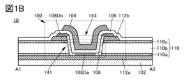
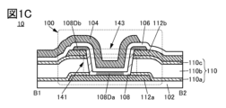
- Fig. 1B and Fig. 1C are cross-sectional views illustrating the example of the semiconductor device.
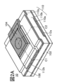
- 2A to 2D are perspective views showing an example of a semiconductor device.
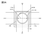
- 3A and 3B are a top view and a cross-sectional view illustrating an example of a semiconductor device.
- FIG. 4 is a cross-sectional view showing an example of a semiconductor device.
- 5A and 5B are diagrams showing an example of the concentration of an impurity element.
- FIG. 6 is a diagram showing an example of the concentration ratio of impurity elements.
- FIG. 7 is a cross-sectional view showing an example of a semiconductor device.
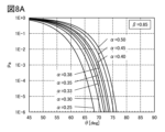
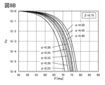
- FIGS. 8A and 8B are diagrams showing an example of the ratio of concentrations of impurity elements.
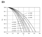
- FIG. 9 is a diagram showing an example of the concentration ratio of impurity elements.
- FIG. 10 is a cross-sectional view showing an example of a semiconductor device.
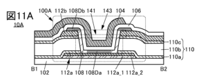
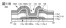
- 11A to 11D are cross-sectional views showing an example of a semiconductor device.
- FIG. 12 is a cross-sectional view showing an example of a semiconductor device.
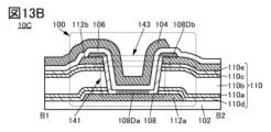
- 13A to 13C are cross-sectional views showing an example of a semiconductor device.
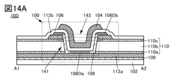
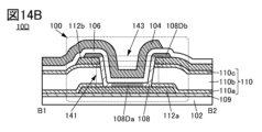
- 14A and 14B are cross-sectional views showing an example of a semiconductor device.
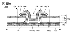
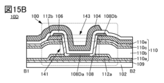
- 15A and 15B are cross-sectional views showing an example of a semiconductor device.
- 16A and 16B are cross-sectional views showing an example of a semiconductor device.
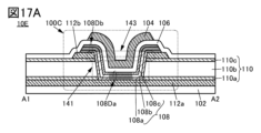
- FIG. 17A and 17B are cross-sectional views showing an example of a semiconductor device.
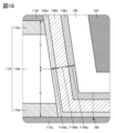
- FIG. 18 is a cross-sectional view showing an example of a semiconductor device.
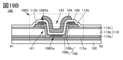
- 19A and 19B are cross-sectional views showing an example of a semiconductor device.
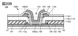
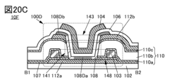
- Fig. 20A is a top view illustrating an example of a semiconductor device, and Fig. 20B and Fig. 20C are cross-sectional views illustrating an example of the semiconductor device.
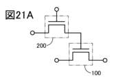
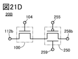
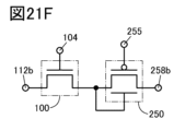
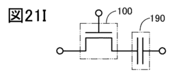
- 21A to 21I are circuit diagrams showing an example of a semiconductor device.
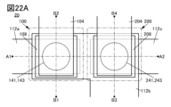
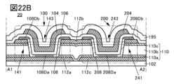
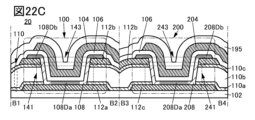
- Fig. 22A is a top view illustrating an example of a semiconductor device, and Fig. 22B and Fig. 22C are cross-sectional views illustrating an example of the semiconductor device.
- Fig. 22A is a top view illustrating an example of a semiconductor device
- Fig. 22B and Fig. 22C are cross-sectional views illustrating an example of the semiconductor device.
- Fig. 22A is a top view illustrating an example of a semiconductor device
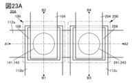
- FIG. 23A is a top view illustrating an example of a semiconductor device
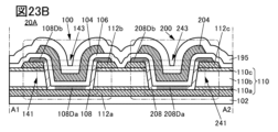
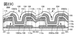
- Fig. 23B and Fig. 23C are cross-sectional views illustrating an example of the semiconductor device.
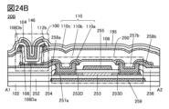
- 24A is a top view illustrating an example of a semiconductor device
- FIG 24B is a cross-sectional view illustrating the example of the semiconductor device.
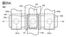
- 25A is a top view illustrating an example of a semiconductor device
- FIG 25B is a cross-sectional view illustrating the example of the semiconductor device.
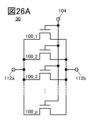
- 26A and 26B are equivalent circuit diagrams of a semiconductor device
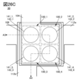
- Fig. 26C is a top view showing an example of the semiconductor device.
- FIG. 27 is a cross-sectional view showing an example of a semiconductor device.
- FIG. 28 is a perspective view showing an example of a semiconductor device.
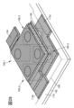
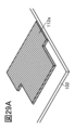
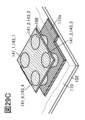
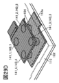
- 29A to 29D are perspective views showing an example of a semiconductor device.
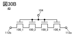
- 30A and 30B are equivalent circuit diagrams of a semiconductor device
- Fig. 30C is a top view showing an example of the semiconductor device.
- FIG. 31 is a cross-sectional view showing an example of a semiconductor device.
- FIG. 32 is a perspective view showing an example of a semiconductor device.
- 33A to 33D are perspective views showing an example of a semiconductor device.
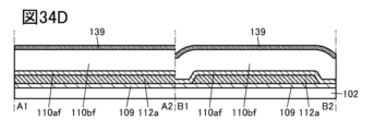
- 34A to 34E are cross-sectional views showing an example of a method for manufacturing a semiconductor device.
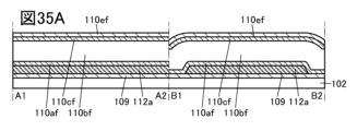
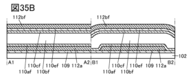
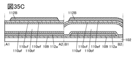
- 35A to 35D are cross-sectional views showing an example of a method for manufacturing a semiconductor device.
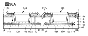
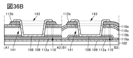
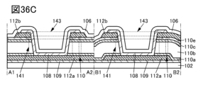
- 36A to 36C are cross-sectional views showing an example of a method for manufacturing a semiconductor device.
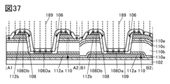
- FIG. 37 is a cross-sectional view showing an example of a method for manufacturing a semiconductor device.
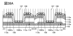
- 38A and 38B are cross-sectional views showing an example of a method for manufacturing a semiconductor device.
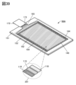
- FIG. 39 is a perspective view showing an example of a display device.
- 40A and 40B are cross-sectional views showing an example of a display device.
- FIG. 41 is a cross-sectional view showing an example of a display device.
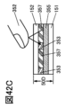
- 42A to 42C are cross-sectional views showing an example of a display device.
- 43A and 43B are cross-sectional views showing an example of a display device.
- FIG. 44 is a cross-sectional view showing an example of a display device.
- FIG. 45 is a cross-sectional view showing an example of a display device.
- FIG. 45 is a cross-sectional view showing an example of a display device.
- 46 is a cross-sectional view showing an example of a display device.
- 47A and 47B are cross-sectional views showing an example of a display device.
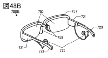
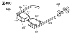
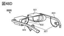
- 48A to 48D are diagrams showing an example of an electronic device.
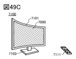
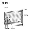
- 49A to 49F are diagrams showing an example of an electronic device.
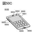
- 50A to 50G are diagrams showing an example of an electronic device.
- ordinal numbers “first” and “second” are used for convenience and do not limit the number of components or the order of the components (e.g., process order or stacking order).
- an ordinal number attached to a component in one place in this specification may not match an ordinal number attached to the same component in another place in this specification or in the claims.
- film and “layer” can be interchanged depending on the circumstances.
- conductive layer can be changed to the term “conductive film.”
- insulating film can be changed to the term “insulating layer.”
- a transistor is a type of semiconductor element that can perform functions such as amplifying current or voltage, and switching operations that control conduction or non-conduction.
- transistor includes IGFETs (Insulated Gate Field Effect Transistors) and thin film transistors (TFTs).
- source and drain may be interchanged when transistors of different polarity are used, or when the direction of current changes during circuit operation. For this reason, in this specification, the terms “source” and “drain” may be used interchangeably. Note that the source and drain of a transistor may be appropriately referred to as the source terminal and drain terminal, or the source electrode and drain electrode, depending on the situation.
- electrically connected includes cases where the connection is made via "something that has some kind of electrical action.”
- something that has some kind of electrical action is not particularly limited as long as it allows the transmission and reception of electrical signals between the connected objects.
- something that has some kind of electrical action includes electrodes or wiring, as well as switching elements such as transistors, resistive elements, coils, and other elements with various functions.
- the off-state current refers to the leakage current between the source and drain when the transistor is in the off state (also called the non-conducting state or cut-off state).
- the off-state refers to a state in which the voltage Vgs between the gate and source is lower than the threshold voltage Vth for an n-channel transistor (higher than Vth for a p-channel transistor).
- top surface shape of a component refers to the contour shape of the component when viewed from above (also called a planar view). Additionally, a top view refers to a view from the normal direction of the surface on which the component is formed, or the surface of the support (e.g., substrate) on which the component is formed.
- top surface shapes roughly match means that at least a portion of the contours of the stacked layers overlap. For example, this includes cases where the upper and lower layers are processed using the same mask pattern, or where parts of the mask pattern are the same. However, strictly speaking, the contours may not overlap, and the upper layer may be located inside the lower layer, or outside the lower layer, in which case it may also be said that “top surface shapes roughly match.” Furthermore, when the top surface shapes match or roughly match, it can also be said that the edges are aligned or roughly aligned.
- a tapered shape refers to a shape in which at least a portion of the side of the structure is inclined with respect to the substrate surface or the surface on which the structure is to be formed.
- the angle between the inclined side and the substrate surface or the surface on which the structure is to be formed is sometimes referred to as a taper angle.
- the side of the structure, the substrate surface, and the surface on which the structure is to be formed do not necessarily need to be completely flat, and may be approximately planar with a slight curvature, or approximately planar with minute irregularities.
- a device manufactured using a metal mask or an FMM may be referred to as a device with an MM (metal mask) structure.
- a device manufactured without using a metal mask or an FMM may be referred to as a device with an MML (metal maskless) structure.
- devices with an MML structure can be manufactured without using a metal mask, they can exceed the upper limit of fineness resulting from the alignment accuracy of the metal mask.
- devices with an MML structure can eliminate the need for equipment related to the manufacture of metal masks and the process of cleaning the metal masks.
- devices with an MML structure are suitable for mass production because they make it possible to keep manufacturing costs low.
- SBS Side By Side
- the SBS structure allows the materials and configuration to be optimized for each light-emitting element, increasing the freedom of material and configuration selection and making it easier to improve brightness and reliability.
- holes or electrons may be referred to as "carriers".
- the hole injection layer or electron injection layer in a light-emitting element may be referred to as a "carrier injection layer”
- the hole transport layer or electron transport layer may be referred to as a “carrier transport layer”
- the hole block layer or electron block layer may be referred to as a "carrier block layer”.
- the above-mentioned carrier injection layer, carrier transport layer, and carrier block layer may not be clearly distinguishable.
- one layer may have two or three functions among the carrier injection layer, carrier transport layer, and carrier block layer.
- the light-emitting element has an EL layer between a pair of electrodes.
- the EL layer has at least a light-emitting layer.
- layers also called functional layers
- the EL layer has include a light-emitting layer, a carrier injection layer (hole injection layer and electron injection layer), a carrier transport layer (hole transport layer and electron transport layer), and a carrier block layer (hole block layer and electron block layer).
- the light-receiving element also called a light-receiving device
- one of the pair of electrodes may be referred to as a pixel electrode, and the other as a common electrode.
- the sacrificial layer (which may also be referred to as a mask layer) is located at least above the light-emitting layer (more specifically, the layer that is processed into an island shape among the layers that make up the EL layer) and has the function of protecting the light-emitting layer during the manufacturing process.
- step discontinuity refers to the phenomenon in which a layer, film, or electrode is separated due to the shape of the surface on which it is formed (e.g., a step, etc.).
- One embodiment of the present invention is a semiconductor device having a semiconductor layer, a first conductive layer, a second conductive layer, a third conductive layer, a first insulating layer, and a second insulating layer.
- the first conductive layer functions as one of a source electrode and a drain electrode of a transistor, and the second conductive layer functions as the other.
- the third conductive layer functions as one of a gate electrode.
- the second insulating layer functions as a gate insulating layer.
- a region of the semiconductor layer in contact with the first conductive layer functions as one of a source region and a drain region, and a region in contact with the second conductive layer functions as the other.
- the first insulating layer is located on the first conductive layer and has a first opening that reaches the first conductive layer.
- the angle between the side of the first opening of the first insulating layer and the top surface of the first conductive layer is 66 degrees or more and 90 degrees or less.
- the second conductive layer is located on the first insulating layer and has a second opening in a region that overlaps with the first opening.
- the semiconductor layer has a first region that contacts the top surface of the first conductive layer in the first opening and a second region that contacts the side of the first insulating layer.
- the semiconductor layer also has a region that contacts the side of the second conductive layer in the second opening and a third region that contacts the top surface of the second conductive layer.
- the second insulating layer is located on the semiconductor layer.
- the third conductive layer has a region that overlaps with the semiconductor layer via the second insulating layer.
- the first region, the third region, and the second insulating layer each contain an impurity element. It is preferable to use a first element as the impurity element. It is preferable to use one or more of the following as the first element: boron, aluminum, indium, carbon, silicon, germanium, tin, phosphorus, arsenic, antimony, magnesium, calcium, titanium, copper, zinc, tungsten, molybdenum, tantalum, hafnium, cerium, and noble gases (helium, neon, argon, krypton, xenon, etc.).
- the electrical resistance of the source and drain regions can be reduced, resulting in a transistor with a large on-current.
- the second region functions as a channel formation region of the transistor.
- the concentration of the first element in the second region is preferably 1 ⁇ 10 ⁇ 3 times or less than the concentration of the first element in the first region.
- the concentration of the first element in the second region is preferably 1 ⁇ 10 ⁇ 3 times or less than the concentration of the first element in the third region.
- the source electrode and drain electrode are located at different heights, and the current flowing through the semiconductor layer flows in the height direction.
- the channel length direction has a component in the height direction (vertical direction), and therefore the transistor according to one embodiment of the present invention can also be called a VFET (Vertical Field Effect Transistor), vertical transistor, vertical channel transistor, vertical channel transistor, etc.
- VFET Vertical Field Effect Transistor
- the transistor can have a source electrode, a semiconductor layer, and a drain electrode that are stacked, so the area occupied can be significantly reduced compared to a so-called planar type transistor in which the semiconductor layer is arranged in a planar shape.
- FIG. 1A shows a top view (also referred to as a plan view) of a semiconductor device 10.
- FIG. 1B shows a cross-sectional view of a cut surface taken along dashed line A1-A2 in FIG. 1A
- FIG. 1C shows a cross-sectional view of a cut surface taken along dashed line B1-B2 in FIG. 1A.
- FIG. 1A some of the components of the semiconductor device 10 (such as a gate insulating layer) are omitted.
- FIG. 1A some of the components are omitted in the top views of the semiconductor device in the following drawings.
- FIGS. 3A and 3B show enlarged views of FIGS. 1A and 1B.
- the semiconductor device 10 has a transistor 100 and an insulating layer 110.
- the semiconductor device 10 is provided on a substrate 102.
- the transistor 100 has a conductive layer 104, an insulating layer 106, a semiconductor layer 108, a conductive layer 112a, and a conductive layer 112b.
- the conductive layer 104 functions as a gate electrode.
- a part of the insulating layer 106 functions as a gate insulating layer.
- the conductive layer 112a functions as one of a source electrode and a drain electrode, and the conductive layer 112b functions as the other.
- a region of the semiconductor layer 108 that overlaps with the gate electrode via the gate insulating layer between the source electrode and the drain electrode functions as a channel formation region.
- a region of the semiconductor layer 108 that is in contact with the source electrode functions as a source region
- a region that is in contact with the drain electrode functions as a drain region.
- a conductive layer 112a is provided on the substrate 102, an insulating layer 110 is provided on the conductive layer 112a, and a conductive layer 112b is provided on the insulating layer 110.
- the insulating layer 110 contacts the conductive layer 112a and the conductive layer 112b and has a region sandwiched between them.
- the conductive layer 112a has a region overlapping with the conductive layer 112b via the insulating layer 110.
- the insulating layer 110 has an opening 141 that reaches the conductive layer 112a. It can also be said that the conductive layer 112a is exposed in the opening 141.
- the conductive layer 112b has an opening 143 in a region overlapping with the conductive layer 112a.
- the opening 143 is provided in a region overlapping with the opening 141.
- the semiconductor layer 108 is provided so as to cover the opening 141 and the opening 143.
- the semiconductor layer 108 has a region in contact with the top surface of the conductive layer 112a and a region in contact with the side surface of the insulating layer 110 in the opening 141, and a region in contact with the side surface of the conductive layer 112b in the opening 143. Furthermore, the semiconductor layer 108 preferably has a region in contact with the top surface of the conductive layer 112b.
- the semiconductor layer 108 has a shape that follows the shapes of the top surface and side surface of the conductive layer 112b, the side surface of the insulating layer 110, and the top surface of the conductive layer 112a.
- the semiconductor material used for the semiconductor layer 108 is not particularly limited.
- a semiconductor made of a single element or a compound semiconductor can be used.
- semiconductors made of a single element include silicon and germanium.
- compound semiconductors include gallium arsenide and silicon germanium.
- Other examples of compound semiconductors include organic semiconductors, nitride semiconductors, and oxide semiconductors (OS: oxide semiconductor). Note that these semiconductor materials may contain impurities as dopants.
- the crystallinity of the semiconductor material used for the semiconductor layer 108 is not particularly limited, and any of an amorphous semiconductor, a single crystal semiconductor, and a semiconductor having crystallinity other than single crystal (a microcrystalline semiconductor, a polycrystalline semiconductor, or a semiconductor having a crystalline region in part) can be used.
- the use of a single crystal semiconductor or a semiconductor having crystallinity is preferable because it can suppress deterioration of the transistor characteristics.
- the semiconductor layer 108 can be made of, for example, silicon.
- silicon examples include single crystal silicon, polycrystalline silicon, microcrystalline silicon, and amorphous silicon.
- polycrystalline silicon examples include low temperature polysilicon (LTPS).
- Transistors using amorphous silicon in the channel formation region can be formed on a large glass substrate and can be manufactured at low cost. Transistors using polycrystalline silicon in the channel formation region have high field effect mobility and can operate at high speed. Furthermore, transistors using microcrystalline silicon in the channel formation region have higher field effect mobility and can operate at high speed than transistors using amorphous silicon.
- the semiconductor layer 108 preferably contains a metal oxide (also referred to as an oxide semiconductor) that exhibits semiconductor characteristics.
- a transistor using an oxide semiconductor (hereinafter referred to as an OS transistor) has an extremely high field-effect mobility compared to a transistor using amorphous silicon.
- an OS transistor has an extremely small off-state current and can hold charge accumulated in a capacitance connected in series with the transistor for a long period of time. Furthermore, by using an OS transistor, the power consumption of a semiconductor device can be reduced.
- the semiconductor layer 108 has a region 108Da in one part and a region 108Db in the other part. Regions 108Da and 108Db each contain an impurity element. Regions 108Da and 108Db each have a higher concentration of the impurity element than other regions of the semiconductor layer 108 (e.g., channel formation regions) and are regions with low electrical resistance (hereinafter also referred to as low resistance regions). In the semiconductor layer 108, the channel formation region is located between regions 108Da and 108Db.
- FIGS. 1B, 1C, and 3B show an example in which region 108Da is formed in a region of semiconductor layer 108 that is in contact with the upper surface of conductive layer 112a, and is located between the upper surface of conductive layer 112a and the lower surface of conductive layer 104.
- the region in which region 108Da is formed is not limited to this, and for example, region 108Da can be formed in the entire region that is in contact with the upper surface of conductive layer 112a.
- the impurity element may diffuse due to heat applied when the impurity element is supplied to semiconductor layer 108 or in a process after the impurity element is supplied.
- region 108Db is formed in a region of semiconductor layer 108 that contacts the top surface of conductive layer 112b.
- Region 108Db can also be provided in a region of semiconductor layer 108 that contacts the side surface of conductive layer 112b.
- Region 108Db can also be provided in a part of a region of semiconductor layer 108 that contacts the side surface of insulating layer 110.
- the first element is used as the impurity element.
- the first element it is preferable to use one or more of boron, aluminum, indium, carbon, silicon, germanium, tin, phosphorus, arsenic, antimony, magnesium, calcium, titanium, copper, zinc, tungsten, molybdenum, tantalum, hafnium, cerium, and noble gases (helium, neon, argon, krypton, xenon, etc.).
- the first element is not limited to the above elements, but may be one or more of the first transition elements (3d transition elements, 3d transition metals), second transition elements (4d transition elements, 4d transition metals), third transition elements (5d transition elements, 5d transition metals), alkaline earth metal elements, and elements contained in the rare earth elements.
- Supplying the first element to the source region and the drain region (also referred to as adding the first element or injecting the first element) generates oxygen vacancies (V O ) in the source region and the drain region. Then, carriers are generated by defects (hereinafter also referred to as V O H) in which hydrogen enters the oxygen vacancies (V O ).
- V O H defects
- the electrical resistance of the semiconductor layer 108, the contact resistance between the semiconductor layer 108 and the conductive layer 112a, and the contact resistance between the semiconductor layer 108 and the conductive layer 112b can each be reduced. Therefore, the on-current of the transistor 100 can be increased. By increasing the on-current, the operating voltage of the transistor 100 can be reduced. This can reduce the power consumption of the semiconductor device.
- the first element When an element that easily bonds with oxygen is used as the first element, the first element takes away oxygen in the semiconductor layer 108 and exists in a state bonded with oxygen. In addition, oxygen vacancies (V 2 O 3 ) are generated in the semiconductor layer 108.
- the first element in the semiconductor layer 108 exists stably in an oxidized state, so that it is difficult to be desorbed by heat or the like applied during the manufacturing process of the transistor 100, and the electrical resistance can be kept low. For this reason, it is preferable to use an element whose oxide can exist in a solid state at least at the temperature during the manufacturing process as the first element.
- typical nonmetallic elements other than hydrogen, typical metallic elements, and transition elements (transition metals) can be mentioned as preferred first elements, and boron, phosphorus, magnesium, aluminum, and silicon can be mentioned as particularly preferred first elements.
- boron, phosphorus, magnesium, aluminum, or silicon it is preferable to use boron, phosphorus, magnesium, aluminum, or silicon as one of the first elements.
- boron or phosphorus it is preferable to use boron or phosphorus as one of the first elements.
- Hydrogen is an ideal impurity element because it not only creates oxygen vacancies but also bonds with oxygen vacancies.
- the impurity element can be preferably supplied by plasma ion doping or ion implantation. These methods allow for highly accurate control of the concentration profile in the depth direction by adjusting the ion acceleration energy and dose.
- ion implantation which ionizes the source gas and supplies the ions after mass separation, it is possible to supply ions of a specific mass, thereby increasing the purity of the supplied impurity element.
- plasma ion doping which supplies ions without mass separation, productivity can be increased.
- boron used as the first element
- BF3 gas can be used as the source gas.
- phosphorus used as the first element
- PH3 gas can be used as the source gas.
- mass-separating the ions generated from these gases and supplying them it is possible to supply ions of a specific mass to the regions 108Da and 108Db, which is more preferable.
- a gas containing the first element and hydrogen (for example, PH 3 gas and B 2 H 6 gas) can be used as the source gas.
- a mixed gas of a gas containing the first element and a gas having hydrogen can be used as the source gas.
- ions generated from the source gas can be supplied without mass separation, which is preferable because it can increase productivity.
- B 2 H 6 gas as the source gas
- boron and hydrogen can be supplied as impurity elements.
- PH 3 gas for example, phosphorus and hydrogen can be supplied as impurity elements.
- the region 108Da preferably includes a portion having an impurity element concentration Na of 1 ⁇ 10 19 atoms/cm 3 or more and 1 ⁇ 10 23 atoms/cm 3 or less, preferably 5 ⁇ 10 19 atoms/cm 3 or more and 5 ⁇ 10 22 atoms/cm 3 or less, and more preferably 5 ⁇ 10 19 atoms/cm 3 or more and 5 ⁇ 10 21 atoms/cm 3 or less.
- the region 108Da when boron is used as the first element, the region 108Da preferably includes a portion having a boron concentration Na in the above-mentioned range.
- the region 108Db preferably includes a portion having an impurity element concentration Nb of 1 ⁇ 10 19 atoms/cm 3 or more and 1 ⁇ 10 23 atoms/cm 3 or less, preferably 5 ⁇ 10 19 atoms/cm 3 or more and 5 ⁇ 10 22 atoms/cm 3 or less, and more preferably 5 ⁇ 10 19 atoms/cm 3 or more and 5 ⁇ 10 21 atoms/cm 3 or less.
- the region 108Db when boron is used as the first element, the region 108Db preferably includes a portion having a boron concentration Nb in the above-mentioned range.
- region 108Da contains two or more impurity elements, it is preferable that at least one of the impurity elements is in the above range. It is also more preferable that the concentration of each impurity element is in the above range. The same applies to region 108Db.
- the impurity elements When the impurity elements are supplied to the regions 108Da and 108Db, the impurity elements may also be supplied to the channel formation region of the semiconductor layer 108. Alternatively, due to heat applied during the manufacturing process, some of the impurity elements contained in the regions 108Da and 108Db may diffuse into the channel formation region.
- the concentration Nc of the impurity element in the channel formation region of the semiconductor layer 108 is preferably low.
- the concentration Nc is preferably lower than the concentration Na of the impurity element in the region 108Da.
- the concentration Nc is preferably lower than the concentration Nb of the impurity element in the region 108Db.
- the concentration Nc is preferably 1 ⁇ 10 ⁇ 1 times or less than the concentration Na, more preferably 1 ⁇ 10 ⁇ 2 times or less, more preferably 1 ⁇ 10 ⁇ 3 times or less, and even more preferably 1 ⁇ 10 ⁇ 4 times or less.
- the concentration Nc is preferably 1 ⁇ 10 ⁇ 1 times or less than the concentration Nb, more preferably 1 ⁇ 10 ⁇ 2 times or less, more preferably 1 ⁇ 10 ⁇ 3 times or less, and even more preferably 1 ⁇ 10 ⁇ 4 times or less.
- the ratio Pa of the concentration Nc to the concentration Na can be expressed by formula (2).
- the ratio Pb of the concentration Nc to the concentration Nb can be expressed by formula (3).
- the ratios Pa and Pb are both dimensionless quantities and real numbers greater than 0.
- Each of the ratios Pa and Pb is preferably 1 ⁇ 10 ⁇ 1 or less, more preferably 1 ⁇ 10 ⁇ 2 or less, further preferably 1 ⁇ 10 ⁇ 3 or less, and further preferably 1 ⁇ 10 ⁇ 4 or less. This allows a transistor to have both a small cutoff current and a large on-current. Therefore, a semiconductor device that has both low power consumption and high performance can be obtained.
- the concentration of impurity elements (here, concentration Na, concentration Nb, and concentration Nc) in the channel formation region, region 108Da, and region 108Db of the semiconductor layer 108 can be analyzed using, for example, secondary ion mass spectrometry (SIMS), X-ray photoelectron spectrometry (XPS), or electron spectrometry for chemical analysis (ESCA).
- SIMS secondary ion mass spectrometry
- XPS X-ray photoelectron spectrometry
- ESCA electron spectrometry for chemical analysis
- concentration distribution in the depth direction can be known by combining ion sputtering from the front side or back side of the sample with XPS analysis.
- the concentration Nc in the channel formation region is low. Therefore, the concentration Nc may be difficult to quantify or may be below the detection limit.
- the impurity element is more easily supplied to the source and drain regions of the semiconductor layer 108 than to the channel formation region.
- the impurity element is preferably supplied from a direction perpendicular or approximately perpendicular to the top surface of the substrate 102.
- the amount of the impurity element supplied to a region inclined with respect to the top surface of the substrate 102 in the semiconductor layer 108 is smaller than that supplied to a region parallel or approximately parallel to the top surface of the substrate 102.
- the amount of the impurity element supplied to the source and drain regions of the semiconductor layer 108 is larger than that supplied to the channel formation region. Therefore, the electrical resistance of the source and drain regions can be preferentially reduced.
- the insulating layer 110 one or both of an inorganic insulating layer and an organic insulating layer can be used.
- examples of materials that can be used for the organic insulating layer include acrylic resin and polyimide resin.
- the insulating layer 110 has one or more inorganic insulating layers. Examples of materials that can be used for the inorganic insulating layer include oxides, nitrides, oxynitrides, and nitride oxides.
- oxides include silicon oxide, aluminum oxide, magnesium oxide, gallium oxide, germanium oxide, yttrium oxide, zirconium oxide, lanthanum oxide, neodymium oxide, hafnium oxide, tantalum oxide, cerium oxide, gallium zinc oxide, and hafnium aluminate.
- nitrides include silicon nitride and aluminum nitride.
- oxynitrides include silicon oxynitride, aluminum oxynitride, gallium oxynitride, yttrium oxynitride, and hafnium oxynitride.
- nitride oxides include silicon nitride oxide and aluminum nitride oxide.
- an oxynitride refers to a material whose composition contains more oxygen than nitrogen.
- An oxynitride refers to a material whose composition contains more nitrogen than oxygen.
- the insulating layer 110 has a region in contact with the semiconductor layer 108.
- a metal oxide is used for the semiconductor layer 108
- the part of the insulating layer 110 in contact with the channel formation region of the semiconductor layer 108 contains oxygen.
- One or more of an oxide and an oxynitride can be suitably used for the part of the insulating layer 110 in contact with the channel formation region of the semiconductor layer 108.
- a metal oxide is used for the semiconductor layer 108
- oxygen is supplied from the insulating layer 110 to the semiconductor layer 108, and oxygen vacancies ( VO ) and VOH in the semiconductor layer 108 can be reduced.
- the insulating layer 106 which functions as a gate insulating layer of the transistor 100, is provided so as to cover the openings 141 and 143.
- the insulating layer 106 is provided on the semiconductor layer 108, the conductive layer 112b, and the insulating layer 110.
- the insulating layer 106 has a region in contact with the top surface and side surfaces of the semiconductor layer 108, the top surface and side surfaces of the conductive layer 112b, and the top surface of the insulating layer 110.
- the insulating layer 106 has a shape that follows the shapes of the top surface of the insulating layer 110, the top surface and side surfaces of the conductive layer 112b, the top surface and side surfaces of the semiconductor layer 108, and the top surface of the conductive layer 112a.
- the thicknesses Ta, Tb, and Tc are thicknesses in a direction perpendicular or approximately perpendicular to the surface on which the insulating layer 106 is formed. More specifically, the thickness Ta is the shortest distance between the upper surface of the semiconductor layer 108 provided along the upper surface of the conductive layer 112a and the upper surface of the insulating layer 106.
- the thickness Tb is the shortest distance between the upper surface of the semiconductor layer 108 provided along the upper surface of the conductive layer 112b and the upper surface of the insulating layer 106.
- the thickness Tc is the shortest distance between the side surface of the semiconductor layer 108 on the insulating layer 106 side provided along the side surface of the insulating layer 110 and the side surface of the insulating layer 106 on the conductive layer 104 side.
- FIG. 3B shows a configuration in which the thicknesses Ta, Tb, and Tc are the same, but one aspect of the present invention is not limited to this. A configuration in which some or all of the thicknesses Ta, Tb, and Tc are different may also be used.
- a part of the insulating layer 106 functions as a gate insulating layer.
- the thickness Tc of the part of the insulating layer 106 in contact with the channel formation region is preferably 1 nm or more and 200 nm or less, more preferably 1 nm or more and 150 nm or less, and even more preferably 1 nm or more and 100 nm or less.
- the thickness Tc is preferably 30 nm or more and 100 nm or less.
- the thickness Tc is preferably 1 nm or more and 50 nm or less.
- the thickness Tc is preferably 1 nm or more and 10 nm or less.
- the conductive layer 104 which functions as the gate electrode of the transistor 100, is provided on the insulating layer 106 and has a region in contact with the top surface of the insulating layer 106.
- the conductive layer 104 has a region that overlaps with the semiconductor layer 108 via the insulating layer 106.
- the conductive layer 104 has a shape that follows the shape of the top surface of the insulating layer 106.
- the transistor 100 is a so-called top-gate transistor having a gate electrode above the semiconductor layer 108. Furthermore, since the bottom surface of the semiconductor layer 108 is in contact with the source electrode and the drain electrode, the transistor 100 can be called a TGBC (Top Gate Bottom Contact) type transistor. Furthermore, the source electrode and the drain electrode of the transistor 100 are located at different heights relative to the surface of the substrate 102 on which the transistor 100 is formed, and the drain current flows in a direction perpendicular to or approximately perpendicular to the surface of the substrate 102. It can also be said that the drain current flows vertically or approximately vertically in the transistor 100. Therefore, the transistor that is one aspect of the present invention can be called a VFET.
- the channel length of the transistor 100 can be controlled by the thickness of the insulating layer 110 provided between the conductive layer 112a and the conductive layer 112b. Therefore, a transistor having a channel length shorter than the minimum exposure dimension of an exposure device used to manufacture the transistor can be manufactured with high precision. In addition, the characteristic variation between multiple transistors 100 is also reduced. This makes it possible to stabilize the operation of the semiconductor device 10 and improve its reliability. Furthermore, reduced characteristic variation of the transistors increases the freedom of circuit design and allows the operating voltage of the semiconductor device to be lowered. This allows the power consumption of the semiconductor device to be reduced.
- the transistor can have a source electrode, a semiconductor layer, and a drain electrode that are stacked, so the area occupied can be significantly reduced compared to a so-called planar type transistor in which the semiconductor layer is arranged in a planar shape.
- the conductive layer 112a, the conductive layer 112b, and the conductive layer 104 can each function as wiring, and the transistor 100 can be provided in a region where these wirings overlap. That is, in a circuit having the transistor 100 and the wiring, the area occupied by the transistor 100 and the wiring can be reduced. Therefore, the area occupied by the circuit can be reduced, and a small-sized semiconductor device can be obtained.
- a semiconductor device of one embodiment of the present invention when a semiconductor device of one embodiment of the present invention is applied to a pixel circuit of a display device, the area occupied by the pixel circuit can be reduced, and a high-definition display device can be obtained.
- a semiconductor device of one embodiment of the present invention when a semiconductor device of one embodiment of the present invention is applied to a driver circuit of a display device (e.g., one or both of a gate line driver circuit and a source line driver circuit), the area occupied by the driver circuit can be reduced, and a display device with a narrow frame can be obtained.
- the insulating layer 110 preferably has a laminated structure.
- FIG. 1B and other figures show an example in which the insulating layer 110 has an insulating layer 110a, an insulating layer 110b on the insulating layer 110a, and an insulating layer 110c on the insulating layer 110b.
- the insulating layers 110a, 110b, and 110c can each be made of the materials listed in the description of the insulating layer 110.
- the region of the semiconductor layer 108 in contact with the insulating layer 110b functions as a channel formation region.
- the insulating layer 110b preferably contains oxygen, and preferably uses one or more of the oxides and oxynitrides described above. Specifically, one or both of silicon oxide and silicon oxynitride can be preferably used for the insulating layer 110b.
- a material that releases oxygen when heated for the insulating layer 110b It is more preferable to use a material that releases oxygen when heated for the insulating layer 110b.
- oxygen can be supplied to the semiconductor layer 108.
- oxygen vacancies (V O ) are repaired and oxygen vacancies (V O ) can be reduced.
- V O H can be reduced. Therefore, a transistor having good electrical characteristics and high reliability can be obtained.
- oxygen can be supplied to the insulating layer 110b by performing a heat treatment in an oxygen-containing atmosphere or a plasma treatment in an oxygen-containing atmosphere.
- oxygen can be supplied to the insulating layer 110b by forming a film on the upper surface of the insulating layer 110b by a sputtering method in an oxygen-containing atmosphere. The film may then be removed. Note that a method for supplying oxygen to the insulating layer 110b will be specifically described in embodiment 2.
- the insulating layer 110b is preferably formed by a deposition method such as a sputtering method or a plasma enhanced chemical vapor deposition (PECVD) method.
- a deposition method such as a sputtering method or a plasma enhanced chemical vapor deposition (PECVD) method.
- PECVD plasma enhanced chemical vapor deposition
- a gas containing hydrogen e.g., hydrogen gas and ammonia gas
- the sputtering method can be particularly preferably used for the insulating layer 110b. This can suppress the supply of hydrogen to the channel formation region, and stabilize the electrical characteristics of the transistor 100.
- the insulating layer 110a is provided between the insulating layer 110b and the conductive layer 112a.
- the insulating layer 110c is provided between the insulating layer 110b and the conductive layer 112b. It is preferable that the amount of impurities (e.g., hydrogen and water) released from the insulating layer 110a and the insulating layer 110c is small. Furthermore, it is preferable that the insulating layer 110a and the insulating layer 110c are each impermeable to substances (e.g., atoms, molecules, and ions). It can be said that the insulating layer 110a and the insulating layer 110c function as a barrier film.
- the insulating layer 110a and the insulating layer 110c are each impermeable to impurities. This makes it possible to suppress the diffusion of impurities contained in the insulating layer 110a and the insulating layer 110c into the channel formation region. Therefore, it is possible to obtain a transistor that exhibits good electrical characteristics and is highly reliable.
- the insulating layer 110a and the insulating layer 110c are preferably made of a material through which oxygen does not easily permeate. This can suppress the oxygen contained in the insulating layer 110b from diffusing to the conductive layer 112a side through the insulating layer 110a. Similarly, the oxygen contained in the insulating layer 110b can suppress the oxygen contained in the insulating layer 110b from diffusing to the conductive layer 112b side through the insulating layer 110c. This can increase the amount of oxygen supplied from the insulating layer 110b to the channel formation region of the semiconductor layer 108, thereby reducing oxygen vacancies (V O ) and V O H in the channel formation region. Therefore, a transistor having good electrical characteristics and high reliability can be obtained.
- the conductive layer 112a is oxidized by the oxygen contained in the insulating layer 110b, and the electrical resistance of the conductive layer 112a is prevented from increasing.
- the conductive layer 112b is oxidized by the oxygen contained in the insulating layer 110b, and the electrical resistance of the conductive layer 112b is prevented from increasing. Therefore, a transistor having a large on-current can be obtained.
- a barrier film refers to a film that has barrier properties.
- Barrier properties refer to one or both of the following functions: making it difficult for a target substance to diffuse, thereby suppressing the substance from permeating the film (also called low permeability), and the function of capturing or fixing the substance (also called gettering).
- an insulating layer that has barrier properties can be called a barrier insulating layer.
- the insulating layer 110a and the insulating layer 110c which function as a barrier film, can each be made of one or more of the following: an oxide having one or both of aluminum and hafnium, an oxide having magnesium, an oxide having gallium, a nitride having silicon, and a nitride oxide having silicon.
- the insulating layer 110a and the insulating layer 110c can each be made of one or more of aluminum oxide, hafnium oxide, hafnium aluminate, magnesium oxide, gallium oxide, gallium zinc oxide, silicon nitride, and silicon nitride oxide.
- the insulating layer 110a and the insulating layer 110c can be made of the same material. Alternatively, the insulating layer 110a and the insulating layer 110c can be made of different materials.
- oxygen can be supplied to insulating layer 110b (or the insulating film that becomes insulating layer 110b) when forming insulating layer 110c (or the insulating film that becomes insulating layer 110c).
- different materials refer to materials in which some or all of the constituent elements are different, or materials in which the constituent elements are the same but the composition is different.
- the impurity element is preferably supplied to the semiconductor layer 108 through the insulating layer 106.
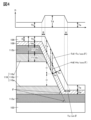
- the supply of the impurity element will be described with reference to FIG. 4.
- the lower side of FIG. 4 shows a cross-sectional view of the insulating layer 106, the semiconductor layer 108, and their vicinity when the impurity element is supplied to the semiconductor layer 108 through the insulating layer 106.
- the impurity element is supplied from a direction perpendicular to the top surface of the substrate 102 will be described. Note that the cross-sectional view shown in FIG.
- FIG 4 shows a configuration in which the surface of the insulating layer 106 (specifically, the top surface and side surface of the insulating layer 106) is parallel to the top surface and side surface of the semiconductor layer 108, which is the surface on which the insulating layer 106 is formed.
- the thickness Td can be the thickness of the insulating layer 106 on a straight line extending from the midpoint between the upper surface end and the lower surface end of the insulating layer 110b in the direction in which the impurity element is supplied (here, the direction perpendicular to the upper surface of the substrate 102).
- the thickness Ta of the region provided along the upper surface of the conductive layer 112a and the thickness Tb of the region provided along the upper surface of the conductive layer 112b are thin.
- the region of the semiconductor layer 108 provided along the upper surface of the conductive layer 112a or the upper surface of the conductive layer 112b receives a larger amount of impurity element than the region provided along the side of the insulating layer 110.
- the supply of the impurity element to the channel formation region of the semiconductor layer 108 can be suppressed, and the electrical resistance of the source region and the drain region can be preferentially reduced.
- the thicker the insulating layer 106 the larger the difference between thickness Ta and thickness Td, and the difference between thickness Tb and thickness Td can be. This can prevent impurity elements from being supplied to the channel formation region of the semiconductor layer 108, and preferentially lower the electrical resistance of the source and drain regions.
- the insulating layer 106 may also contain the impurity elements. It is preferable that each of the regions 108Da and 108Db has a portion with a higher concentration of the impurity element than the insulating layer 106, since this can reduce the electrical resistance of the regions 108Da and 108Db.
- concentration of the impurity element in the insulating layer 106 please refer to the description related to the analysis of the concentration of the impurity element in the semiconductor layer 108.
- the insulating layer 106 preferably has an insulating layer containing oxygen.
- the impurity element exists in a state of being bonded with oxygen in the insulating layer 106 as in the semiconductor layer 108.
- oxygen and the impurity element are bonded and stabilized, oxygen is less likely to be released from the region containing the impurity element even when heat is applied, so that the diffusion of oxygen to other layers can be suppressed.
- This makes it possible to efficiently supply oxygen to the channel formation region while suppressing the supply of oxygen from the insulating layer 106 to the regions 108Da and 108Db. Therefore, oxygen deficiency in the channel formation region can be reduced while preventing the electrical resistance of the regions 108Da and 108Db from increasing. As a result, a transistor with good electrical characteristics and high reliability can be realized.
- the boron contained in the regions 108Da, 108Db, and the insulating layer 106 may exist in a state of being bonded to oxygen. This can be confirmed, for example, by observing a peak due to a B 2 O 3 bond in an XPS analysis. In addition, in the XPS analysis, a spectrum peak due to the state in which the boron element exists alone is not observed, or the peak intensity is extremely small, to the level of background.
- the impurity element When an impurity element is supplied to the semiconductor layer 108 through the insulating layer 106, the impurity element penetrates from the surface of the insulating layer 106, passes through the insulating layer 106, and then reaches the semiconductor layer 108 through the interface between the insulating layer 106 and the semiconductor layer 108.
- the thickness of the insulating layer 106 in the direction in which the impurity element is supplied can also be said to be the depth D from the surface of the insulating layer 106 to the semiconductor layer 108.
- the depth D in each region of the insulating layer 106 is shown in the upper part of FIG. 4.
- the horizontal axis indicates the position of the insulating layer 106 in a cross-sectional view
- the vertical axis indicates the depth D.
- the depth D in the region provided along the upper surface of the conductive layer 112a of the insulating layer 106 corresponds to the thickness Ta of the insulating layer 106.
- the depth D in the region provided along the upper surface of the conductive layer 112b of the insulating layer 106 corresponds to the thickness Tb of the insulating layer 106.
- the depth D in the region provided along the side surface of the insulating layer 110 of the insulating layer 106 corresponds to the thickness Td.
- the impurity element is supplied to the semiconductor layer 108 through the insulating layer 106
- the insulating layer 106 and the semiconductor layer 108 may each be referred to as an implanted layer.
- the depth "Td” in the region of insulating layer 106 that is provided along the side surface of insulating layer 110 is deeper than the depth "Ta” in the region that is provided along the top surface of conductive layer 112a, and is deeper than the depth "Tb” in the region that is provided along the top surface of conductive layer 112b.
- depth D has a value between "Ta” and "Td”
- depth D has a value between "Tb” and "Td”.
- depth D has a value smaller than "Td”.
- the concentration of the impurity element can be expressed by a Gaussian distribution.
- the concentration N(x) of the impurity element at depth x can be expressed by formula (4).
- the concentration N(x) is a real number greater than 0.
- Q is the dose
- m is the projected range (also referred to as Rp)
- s is the standard deviation in the depth direction (also referred to as ⁇ Rp).
- the dose Q, projected range m, and standard deviation s are all real numbers greater than 0. Note that the projected range m is the average depth at which ions stop during implantation, and the concentration of the impurity element is highest at depth "m.”
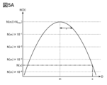
- the Gaussian distribution of the concentration of an impurity element at a projected range m and a standard deviation s (variance s2 ) is shown in Figure 5A.
- the horizontal axis indicates the depth D on a linear scale
- the vertical axis indicates the concentration N(D) on a logarithmic scale.
- the concentration N(m) is highest at a projected range m, which is indicated as " Nmax " in Figure 5A.
- the projected range m and standard deviation s can be calculated, for example, using simulation software.
- the simulation software include TRIM (Transport of Ion in Matter) and SRIM (Stopping and Range of Ions in Matter). These are software that simulate the ion implantation process using the Monte Carlo method.
- the type of impurity element supplied (specifically, the type of ion), the composition and film density of the implanted layer, and the acceleration energy can be used as simulation parameters. For example, if the mass number of the impurity element supplied is large, the projected range m becomes small.
- the stopping power in ion implantation differs depending on the type of element, the projected range m differs depending on the composition of the implanted layer.
- the projected range m can be made different depending on the material used for the implanted layer (e.g., the insulating layer 106). Note that film density refers to the mass per unit volume. Also, if the acceleration energy is high, the projected range m will be large and the standard deviation s will be large.
- the concentration Na of the impurity element in region 108Da is the concentration of the impurity element at depth "Ta” and can be expressed by formula (5).
- the concentration Nb of the impurity element in region 108Db is the concentration of the impurity element at depth "Tb” and can be expressed by formula (6).
- the concentration Nc of the impurity element in the channel formation region is the concentration of the impurity element at depth "Td” and can be expressed by formula (7).
- the concentrations Na, Nb, and Nc are each real numbers greater than 0.
- the ratio Pa of the impurity element concentration Nc in the channel formation region to the impurity element concentration Na in region 108Da can be expressed by formula (8).
- the ratio Pb of the impurity element concentration Nc in the channel formation region to the impurity element concentration Nb in region 108Db can be expressed by formula (9).
- the ratio Pa can be expressed by thickness Ta, thickness Td, projected range m, and standard deviation s, as shown in formula (8).
- the ratio Pb can be expressed by thickness Tb, thickness Td, projected range m, and standard deviation s, as shown in formula (9). It is preferable to set thickness Ta, thickness Tb, thickness Td, projected range m, and standard deviation s so that ratio Pa and ratio Pab are each within the aforementioned range. As shown in formula (8), the ratio Pa can be made smaller as the difference between thickness Td and thickness Ta is increased. As shown in formula (9), the ratio Pb can be made smaller as the difference between thickness Td and thickness Tb is increased.
- the thickness Td can be expressed by formula (10).
- the angle ⁇ is greater than 0 degrees and less than 90 degrees, cos ⁇ is greater than 0 and less than 1. Therefore, the thickness Td is thicker than the thickness Tc.
- the smaller the angle ⁇ the thinner the thickness Td is, and the larger the angle ⁇ , the thicker the thickness Td is.
- the larger the angle ⁇ the greater the difference between the thickness Td and the thickness Ta can be, and the smaller the ratio Pa can be.
- the larger the angle ⁇ the greater the difference between the thickness Td and the thickness Tb can be, and the smaller the ratio Pb can be.
- the angle ⁇ is preferably equal to or less than 90 degrees, and more preferably less than 90 degrees.
- the cross-sectional view shown in FIG. 4 shows a configuration in which the upper surface of the conductive layer 112a is parallel to the upper surface of the substrate 102.
- the angle ⁇ is the same as the angle between the side surface of the insulating layer 110 and the upper surface of the substrate 102.
- the impurity element is preferably supplied from a direction perpendicular or approximately perpendicular to the upper surface of the conductive layer 112a. In other words, the impurity element is preferably supplied from a direction perpendicular or approximately perpendicular to the upper surface of the substrate 102.
- the impurity element is preferably supplied from a direction perpendicular or approximately perpendicular to the upper surface of the conductive layer 112a.
- the ratio Pa can be expressed by formula (11), and the ratio Pb can be expressed by formula (12).
- the ratio Pa can be expressed by the angle ⁇ , thickness Ta, thickness Tc, projected range m, and standard deviation s, as shown in formula (11).
- the ratio Pb can be expressed by the angle ⁇ , thickness Tb, thickness Tc, projected range m, and standard deviation s, as shown in formula (12). It is preferable to set the angle ⁇ , thickness Ta, thickness Tb, thickness Tc, projected range m, and standard deviation s so that the ratio Pa and the ratio Pab are each within the aforementioned range.
- the ratio Pa and the ratio Pb can be made smaller as the angle ⁇ increases.
- the concentration N(D) of the impurity element is highest at the interface between the insulating layer 106 and the semiconductor layer 108 in the region provided along the top surface of the conductive layer 112a, and at the interface between the insulating layer 106 and the semiconductor layer 108 in the region provided along the top surface of the conductive layer 112b. It is also assumed that the thicknesses Ta, Tb, and Tc are the same. In other words, if the projected range m is "Ta”, then as shown in FIG. 5B, the concentration Na at the depth "Ta” and the concentration Nb at the depth "Tb” are highest. If the thickness Td is expressed as "Ta/cos ⁇ ", the ratio Pa can be expressed by formula (13), and the ratio Pb can be expressed by formula (14).
- the ratios Pa and Pb can be expressed by the angle ⁇ , the thickness Ta, and the standard deviation s, respectively. It is preferable to set the angle ⁇ , the thickness Ta, and the standard deviation s so that the ratios Pa and Pab are each within the aforementioned ranges. Note that when the thicknesses Ta and Tb are different from each other, the ratio Pb can be calculated by using formula (12).
- the projected range m and standard deviation s are determined by selecting the acceleration energy according to the type of impurity element supplied, the composition, film density, and thickness of the implanted layer, and the standard deviation s can be expressed by formula (15).
- ⁇ is the ratio of the standard deviation s to the projected range m, and is a dimensionless quantity.
- ⁇ is a real number greater than 0.
- the ratio ⁇ is determined by selecting the acceleration energy according to the type of impurity element supplied, the composition, film density, and thickness of the implanted layer. Using the ratio ⁇ , the ratio Pa can be expressed by formula (16), and the ratio Pb can be expressed by formula (17).
- the ratios Pa and Pb can be expressed by the angle ⁇ and the ratio ⁇ of the standard deviation s to the projected range m, respectively. It is preferable to set the angle ⁇ according to the ratio ⁇ so that the ratios Pa and Pb are each within the aforementioned range. As shown in formulas (16) and (17), the larger the ratio ⁇ , the larger the angle ⁇ can be made to make the ratio Pa smaller. This makes it possible to obtain a transistor that has both a small cutoff current and a large on-current. Therefore, it is possible to obtain a semiconductor device that has both low power consumption and high performance.
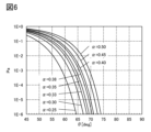
- Figure 6 The relationship between the angle ⁇ and the ratio Pa is shown in Figure 6.
- the horizontal axis represents the angle ⁇
- the vertical axis represents the ratio Pa.
- Figure 6 shows the ratio Pa when the ratio ⁇ is varied to 0.25, 0.30, 0.33, 0.35, 0.38, 0.40, 0.45, and 0.50.
- the angle ⁇ is set to 59 degrees or more, when the ratio ⁇ is 0.30 or less, the angle ⁇ is set to 62 degrees or more, when the ratio ⁇ is 0.33 or less, the angle ⁇ is set to 64 degrees or more, when the ratio ⁇ is 0.35 or less, the angle ⁇ is set to 65 degrees or more, when the ratio ⁇ is 0.38 or less, the angle ⁇ is set to 66 degrees or more, when the ratio ⁇ is 0.40 or less, the angle ⁇ is set to 67 degrees or more, when the ratio ⁇ is 0.45 or less, the angle ⁇ is set to 69 degrees or more, and when the ratio ⁇ is 0.50 or less, the angle ⁇ is set to 70 degrees or more, which is preferable because it is possible to set the ratio Pa to 1 ⁇ 10 ⁇ 3 or less.
- the angle ⁇ is 62 degrees or more, when the ratio ⁇ is 0.30 or less, the angle ⁇ is 65 degrees or more, when the ratio ⁇ is 0.33 or less, the angle ⁇ is 66 degrees or more, when the ratio ⁇ is 0.35 or less, the angle ⁇ is 67 degrees or more, when the ratio ⁇ is 0.38 or less, the angle ⁇ is 68 degrees or more, when the ratio ⁇ is 0.40 or less, the angle ⁇ is 69 degrees or more, when the ratio ⁇ is 0.45 or less, the angle ⁇ is 71 degrees or more, and when the ratio ⁇ is 0.50 or less, the angle ⁇ is 72 degrees or more, thereby making it possible to set the ratio Pa to 1 x 10⁻⁴ or less, which is even more preferable.
- ratio Pa and ratio Pb will also be the same or approximately the same, so ratio Pa in FIG. 6 and the above description can be replaced with ratio Pb.
- the ratios Pa and Pb are 1.6 ⁇ 10 ⁇ 3 when the angle ⁇ is 65 degrees, the ratios Pa and Pb are 6.3 ⁇ 10 ⁇ 4 when the angle ⁇ is 66 degrees, and the ratios Pa and Pb are 6.4 ⁇ 10 ⁇ 5 when the angle ⁇ is 68 degrees. Therefore, by setting the angle ⁇ to 66 degrees or more, the ratios Pa and Pb can each be set to 1 x 10⁻³ or less, and by setting the angle ⁇ to 68 degrees or more, the ratios Pa and Pb can each be set to 1 x 10⁻⁴ or less.
- the ratios Pa and Pb can be reduced. Furthermore, depending on the impurity element used and the film density of the insulating layer 106, by increasing the angle ⁇ , the ratios Pa and Pb can be reduced.
- the thickness Tc can be expressed by the formula (18) using the thickness Ta.
- ⁇ is the ratio of the thickness Tc to the thickness Ta, and is a dimensionless quantity.
- the ratio ⁇ is a real number greater than 0.
- the ratio ⁇ is 1.
- the thickness Tc of the insulating layer 106 in the region provided along the side surface of the insulating layer 110 may be thinner than the thickness Ta of the insulating layer 106 in the region provided along the upper surface of the conductive layer 112a.
- the ratio ⁇ is a real number greater than 0 and less than 1.
- the ratio ⁇ is a real number greater than 1.
- the thickness Tc may be thinner than the thickness Ta, that is, the ratio ⁇ may be smaller than 1.
- the ratio ⁇ can be closer to 1.
- the thickness Tc when the thickness Tc is expressed by formula (18), the thickness Td can be expressed by formula (19). Furthermore, the ratio Pa shown in formula (11) above can be expressed by formula (20). The ratio Pb shown in formula (12) can be expressed by formula (21).
- the ratio Pa can be expressed by the ratio ⁇ , the angle ⁇ , the thickness Ta, the projected range m, and the standard deviation s, as shown in formula (20).
- the ratio Pb can be expressed by the ratio ⁇ , the thickness Ta, the thickness Tb, the projected range m, and the standard deviation s, as shown in formula (21). It is preferable to set the angle ⁇ , the thickness Ta, the thickness Tb, the projected range m, and the standard deviation s according to the ratio ⁇ so that the ratio Pa and the ratio Pab are each within the above-mentioned range.
- the smaller the ratio ⁇ the larger the angle ⁇ can be to reduce the ratio Pa. This allows a transistor that has both a small cutoff current and a large on-current. Therefore, a semiconductor device that has both low power consumption and high performance can be obtained.
- the concentration N of the impurity element is highest at the interface between the insulating layer 106 and the semiconductor layer 108. Also, it is assumed that the thicknesses Ta and Tb are the same. In other words, if the projected range m is "Ta", the ratio Pa can be expressed by formula (22) and the ratio Pb can be expressed by formula (23).
- the ratios Pa and Pb can be expressed by the ratio ⁇ , the thickness Ta, the angle ⁇ , and the standard deviation s, respectively. It is preferable to set the angle ⁇ , the thickness Ta, and the standard deviation s according to the ratio ⁇ so that the ratios Pa and Pab are each within the aforementioned ranges.
- the ratios Pa and Pb can be expressed by the ratio ⁇ of the standard deviation s to the projected range m, the ratio ⁇ of the thickness Tc to the thickness Ta, and the angle ⁇ , respectively. It is preferable to set the angle ⁇ according to the ratio ⁇ and the ratio ⁇ so that the ratios Pa and Pb are each within the aforementioned range.
- the ratio Pa when ⁇ is set to 1 in formula (24) is the aforementioned formula (16).
- the ratio Pb when ⁇ is set to 1 in formula (25) is the aforementioned formula (17).
- Figures 8A and 8B The relationship between the angle ⁇ and the ratio Pa is shown in Figures 8A and 8B.
- Figure 8A shows the relationship between the angle ⁇ and the ratio Pa when the ratio ⁇ is 0.85
- Figure 8B shows the relationship between the angle ⁇ and the ratio Pa when the ratio ⁇ is 0.75.
- the horizontal axis shows the angle ⁇
- the vertical axis shows the ratio Pa.
- Figures 8A and 8B show the ratio Pa when the ratio ⁇ is changed to 0.25, 0.30, 0.33, 0.35, 0.38, 0.40, 0.45, and 0.50, respectively.
- Figure 6 shows the relationship between the angle ⁇ and the ratio Pa when the ratio ⁇ is 1.
- the angle ⁇ is 64 degrees or more, if the ratio ⁇ is 0.30 or less, the angle ⁇ is 67 degrees or more, if the ratio ⁇ is 0.33 or less, the angle ⁇ is 68 degrees or more, if the ratio ⁇ is 0.35 or less, the angle ⁇ is 69 degrees or more, if the ratio ⁇ is 0.38 or less, the angle ⁇ is 70 degrees or more, if the ratio ⁇ is 0.40 or less, the angle ⁇ is 71 degrees or more, if the ratio ⁇ is 0.45 or less, the angle ⁇ is 72 degrees or more, and if the ratio ⁇ is 0.50 or less, the angle ⁇ is 73 degrees or more, thereby making it possible to set the ratio Pa to 1 ⁇ 10 ⁇ 3 or less, which is preferable.
- the angle ⁇ is 66 degrees or more, when the ratio ⁇ is 0.30 or less, the angle ⁇ is 69 degrees or more, when the ratio ⁇ is 0.33 or less, the angle ⁇ is 70 degrees or more, when the ratio ⁇ is 0.35 or less, the angle ⁇ is 71 degrees or more, when the ratio ⁇ is 0.38 or less, the angle ⁇ is 72 degrees or more, when the ratio ⁇ is 0.40 or less, the angle ⁇ is 72 degrees or more, when the ratio ⁇ is 0.45 or less, the angle ⁇ is 74 degrees or more, and when the ratio ⁇ is 0.50 or less, the angle ⁇ is 75 degrees or more, thereby making it possible to set the ratio Pa to 1 x 10⁻⁴ or less, which is even more preferable.
- the angle ⁇ is 68 degrees or more, if the ratio ⁇ is 0.30 or less, the angle ⁇ is 70 degrees or more, if the ratio ⁇ is 0.33 or less, the angle ⁇ is 71 degrees or more, if the ratio ⁇ is 0.35 or less, the angle ⁇ is 71 degrees or more, if the ratio ⁇ is 0.38 or less, the angle ⁇ is 72 degrees or more, if the ratio ⁇ is 0.40 or less, the angle ⁇ is 73 degrees or more, if the ratio ⁇ is 0.45 or less, the angle ⁇ is 74 degrees or more, and if the ratio ⁇ is 0.50 or less, the angle ⁇ is 75 degrees or more, which is preferable.
- the angle ⁇ is 69 degrees or more, when the ratio ⁇ is 0.30 or less, the angle ⁇ is 71 degrees or more, when the ratio ⁇ is 0.33 or less, the angle ⁇ is 72 degrees or more, when the ratio ⁇ is 0.35 or less, the angle ⁇ is 73 degrees or more, when the ratio ⁇ is 0.38 or less, the angle ⁇ is 74 degrees or more, when the ratio ⁇ is 0.40 or less, the angle ⁇ is 74 degrees or more, when the ratio ⁇ is 0.45 or less, the angle ⁇ is 76 degrees or more, and when the ratio ⁇ is 0.50 or less, the angle ⁇ is 77 degrees or more, whereby the ratio Pa can be set to 1 x 10⁻⁴ or less, which is even more preferable.
- ratio Pa and ratio Pb are the same or approximately the same, so ratio Pa in Figures 8A and 8B and the above description can be replaced with ratio Pb.
- the difference between the thickness Td and the thickness Ta of the insulating layer 106 is large. It is preferable that the difference between the thickness Td and the thickness Tb of the insulating layer 106 is large. In other words, it is preferable that the ratio of the thickness Td to the thickness Ta is large. It is preferable that the ratio of the thickness Td to the thickness Tb is large.
- the thickness Td can be expressed by the formula (26) using the thickness Ta.
- ⁇ is the ratio of the thickness Td to the thickness Ta, and is a dimensionless quantity.
- the ratio ⁇ is a real number greater than 0.
- the ratio ⁇ corresponds to " ⁇ /cos ⁇ " in the formula (19).
- the ratio Pa can be expressed by the formula (27). If the thicknesses Tb and Ta of the insulating layer 106 are the same, the ratio Pb can be expressed by the formula (28).
- the ratios Pa and Pb can be expressed by the ratio ⁇ of the standard deviation s to the projected range m, and the ratio ⁇ of the thickness Td to the thickness Ta of the insulating layer 106, respectively. It is preferable to set the ratio ⁇ according to the ratio ⁇ so that the ratios Pa and Pb are each within the aforementioned range. As shown in formulas (27) and (28), the larger the ratio ⁇ , the smaller the ratios Pa and Pb can be. In other words, the larger the ratio of the thickness Td to the thickness Ta, the smaller the ratios Pa and Pb can be.
- Figure 9 shows the relationship between the ratio ⁇ and the ratio Pa.
- the horizontal axis represents the angle ⁇
- the vertical axis represents the ratio Pa.
- Figure 9 shows the ratio Pa when the ratio ⁇ is varied to 0.25, 0.30, 0.33, 0.35, 0.38, 0.40, 0.45, and 0.50.
- the ratio ⁇ when the ratio ⁇ is 0.25 or less, the ratio ⁇ is set to 2.0 or more, when the ratio ⁇ is 0.30 or less, the ratio ⁇ is set to 2.2 or more, when the ratio ⁇ is 0.33 or less, the ratio ⁇ is set to 2.3 or more, when the ratio ⁇ is 0.35 or less, the ratio ⁇ is set to 2.4 or more, when the ratio ⁇ is 0.38 or less, the ratio ⁇ is set to 2.5 or more, when the ratio ⁇ is 0.40 or less, the ratio ⁇ is set to 2.5 or more, when the ratio ⁇ is 0.45 or less, the ratio ⁇ is set to 2.7 or more, and when the ratio ⁇ is 0.50 or less, the ratio ⁇ is set to 2.9 or more, which is preferable to make the ratio Pa 1 ⁇ 10 ⁇ 3 or less.
- the ratio ⁇ is set to 2.1 or more, when the ratio ⁇ is 0.30 or less, the ratio ⁇ is set to 2.3 or more, when the ratio ⁇ is 0.33 or less, the ratio ⁇ is set to 2.5 or more, when the ratio ⁇ is 0.35 or less, the ratio ⁇ is set to 2.6 or more, when the ratio ⁇ is 0.38 or less, the ratio ⁇ is set to 2.7 or more, when the ratio ⁇ is 0.40 or less, the ratio ⁇ is set to 2.8 or more, when the ratio ⁇ is 0.45 or less, the ratio ⁇ is set to 3.0 or more, and when the ratio ⁇ is 0.50 or less, the ratio ⁇ is set to 3.2 or more, whereby the ratio Pa can be set to 1 ⁇ 10-4 or less, which is even more preferable.
- ratio Pa and ratio Pb will also be the same or approximately the same, so ratio Pa in FIG. 9 and the above description can be replaced with ratio Pb.
- the ratio Pa and the ratio Pb can each be set to 1 ⁇ 10 ⁇ 3 or less, and by setting the ratio ⁇ to 2.7 degrees or more, the ratio Pa and the ratio Pb can each be set to 1 ⁇ 10 ⁇ 4 or less.
- the ratios Pa and Pb can be reduced. Furthermore, depending on the impurity element used and the film density of the insulating layer 106, by increasing the ratio ⁇ , the ratios Pa and Pb can be reduced.
- the amount of impurity element supplied to the channel formation region is small. More specifically, it is preferable that the amount of impurity element supplied to the region of the semiconductor layer 108 that contacts the insulating layer 110b is small. Therefore, in a cross-sectional view, it is more preferable that the thickness Te of the insulating layer 106 on a straight line extending from the top surface end of the insulating layer 110b in the direction in which the impurity element is supplied (here, the direction perpendicular to the top surface of the substrate 102) is large. It is more preferable that the thickness Te is at least the same as the thickness Td, or approximately the same as the thickness Td.
- the thickness Ha, Hb, and Hc are thicknesses in a direction perpendicular or approximately perpendicular to the surface on which the semiconductor layer 108 is formed. More specifically, the thickness Ha is the shortest distance between the upper surface of the conductive layer 112a and the upper surface of the semiconductor layer 108. The thickness Hb is the shortest distance between the upper surface of the conductive layer 112b and the upper surface of the semiconductor layer 108.
- the thickness Hc is the shortest distance between the side of the insulating layer 110 and the side of the semiconductor layer 108 on the insulating layer 106 side. Although the thicknesses Ha, Hb, and Hc are the same in FIG. 4 and FIG. 7, one embodiment of the present invention is not limited thereto. The thicknesses Ha, Hb, and Hc may be configured to be partially or entirely different.
- the sum of the thickness Tb of the insulating layer 106 provided along the upper surface of the insulating layer 110b, the thickness Hb of the semiconductor layer 108, the thickness T112b of the conductive layer 112b, and the thickness T110c of the insulating layer 110c is K.
- the sum K is the distance between the upper surface of the insulating layer 106 provided along the upper surface of the conductive layer 112b and the upper surface of the insulating layer 110b in the direction in which the impurity element is supplied (here, the direction perpendicular to the upper surface of the substrate 102). If the sum K is small, the thickness Te of the insulating layer 106 may be thinner than the thickness Td (see region B in FIG. 4 or FIG. 7).
- the sum K is thick. Also, as shown in formula (30), the sum of the thickness Hd of the semiconductor layer 108 and the thickness Td of the insulating layer 106 is L. As shown in formula (31), the sum K is preferably equal to or greater than the sum L. This allows the thickness Te of the insulating layer 106 to be thick.
- the thicknesses Tb and Td of the insulating layer 106, the thicknesses Hb and Hd of the semiconductor layer 108, the thickness T112b of the conductive layer 112b, and the thickness T110c of the insulating layer 110c so as to satisfy formula (31).
- the thickness Td can be expressed by formula (32). If the thicknesses Hb and Hc of the semiconductor layer 108 are the same, the thickness Hd can be expressed by formula (33). The sum L can be expressed by formula (34).
- the angle ⁇ when the angle ⁇ is greater than 0 degrees and less than 90 degrees, it is preferable to increase the sum of the thickness T112b of the conductive layer 112b and the thickness T110c of the insulating layer 110c as the angle ⁇ increases. Specifically, it is preferable to increase one or both of the thickness T112b of the conductive layer 112b and the thickness T110c of the insulating layer 110c as the angle ⁇ increases.
- the angle ⁇ is 60 degrees or less, it is more preferable that the sum of the thickness T112b of the conductive layer 112b and the thickness T110c of the insulating layer 110c is at least equal to or greater than the sum of the thickness Tb of the insulating layer 106 and the thickness Hb of the semiconductor layer 108.
- the angle ⁇ is 65 degrees or less, it is more preferable that the sum of the thickness T112b of the conductive layer 112b and the thickness T110c of the insulating layer 110c is at least 1.4 times the sum of the thickness Tb of the insulating layer 106 and the thickness Hb of the semiconductor layer 108.
- the angle ⁇ is 70 degrees or less, it is more preferable that the sum of the thickness T112b of the conductive layer 112b and the thickness T110c of the insulating layer 110c is at least 2.0 times the sum of the thickness Tb of the insulating layer 106 and the thickness Hb of the semiconductor layer 108.
- the angle ⁇ is 75 degrees or less, it is more preferable that the sum of the thickness T112b of the conductive layer 112b and the thickness T110c of the insulating layer 110c is at least 2.9 times the sum of the thickness Tb of the insulating layer 106 and the thickness Hb of the semiconductor layer 108.
- the angle ⁇ is 80 degrees or less, it is more preferable that the sum of the thickness T112b of the conductive layer 112b and the thickness T110c of the insulating layer 110c is at least 4.8 times the sum of the thickness Tb of the insulating layer 106 and the thickness Hb of the semiconductor layer 108.
- the thicknesses Tb and Tc of the insulating layer 106 are the same, and the thicknesses Hb and Hc of the semiconductor layer 108 are the same, one embodiment of the present invention is not limited to this.
- a configuration in which the thicknesses Tb and Tc are different from each other is also possible.
- a configuration in which the thicknesses Hb and Hc are different from each other is also possible. Even in such cases, it is preferable to set the thicknesses of each layer so as to satisfy formula (31).
- the thickness Tc of the insulating layer 106 is 0.85 times the thickness Tb
- the thickness Hc of the semiconductor layer 108 is 0.85 times the thickness Hb.
- the sum L can be expressed as "0.85 x (Tb + Hb) / cos ⁇ ", which can be applied to formula (31).
- the angle ⁇ is 60 degrees or less, it is more preferable that the sum of the thickness T112b of the conductive layer 112b and the thickness T110c of the insulating layer 110c is at least 0.7 times the sum of the thickness Tb of the insulating layer 106 and the thickness Hb of the semiconductor layer 108.
- the angle ⁇ is 65 degrees or less, it is more preferable that the sum of the thickness T112b of the conductive layer 112b and the thickness T110c of the insulating layer 110c is at least 1.1 times the sum of the thickness Tb of the insulating layer 106 and the thickness Hb of the semiconductor layer 108.
- the sum of the thickness T112b of the conductive layer 112b and the thickness T110c of the insulating layer 110c is more preferably at least 1.5 times the sum of the thickness Tb of the insulating layer 106 and the thickness Hb of the semiconductor layer 108.
- the sum of the thickness T112b of the conductive layer 112b and the thickness T110c of the insulating layer 110c is more preferably at least 2.3 times the sum of the thickness Tb of the insulating layer 106 and the thickness Hb of the semiconductor layer 108.
- the sum of the thickness T112b of the conductive layer 112b and the thickness T110c of the insulating layer 110c is more preferably at least 3.9 times the sum of the thickness Tb of the insulating layer 106 and the thickness Hb of the semiconductor layer 108.
- the concentration ratios Pa and Pb of the impurity elements are small.
- the angle ⁇ can be determined so that the ratios Pa and Pb are each within the ranges mentioned above.
- Region 108Da and region 108Db can each be configured to have a second element in addition to a first element as an impurity element.
- the second element is different from the first element.
- the second element one or more of the elements that can be used as the first element described above can be used. It is preferable that the second element has a larger mass number than the first element. It is also preferable that the first element is easily bonded to oxygen. For example, boron or phosphorus can be used as the first element, and argon, krypton, or xenon can be used as the second element.
- the first element can be supplied to the semiconductor layer 108.
- the mass number of the supplied element is large, the number of metal-oxygen bonds broken in the metal oxide of the semiconductor layer 108 increases. Furthermore, oxygen vacancies (V 2 O 3 ) occur in the region that will become the region 108Da and the region that will become the region 108Db due to the breaking of the metal-oxygen bonds.
- oxygen vacancies are generated in the channel formation region, which may increase VOH and increase the carrier concentration.
- concentration of the second element in the channel formation region is preferably lower than the concentration of the second element in the region 108Da.
- the concentration of the second element in the channel formation region is preferably lower than the concentration of the second element in the region 108Db.
- the second element is preferably supplied to the semiconductor layer 108 through the insulating layer 106.
- the first element is preferably supplied to the semiconductor layer 108 through the insulating layer 106.
- the insulating layer 106 may also contain the second impurity element.
- the second element is preferably supplied from a direction perpendicular or approximately perpendicular to the upper surface of the substrate 102.
- the second element can be supplied by a method that can be used to supply the first element.
- plasma ion doping or ion implantation can be preferably used to supply the second element.
- the amount of the second element supplied to the channel formation region can be reduced by setting the angle ⁇ of the insulating layer 110 or the thickness Td of the insulating layer 106 to the above-mentioned range, which is preferable.
- the acceleration energy when supplying the second element is higher than the acceleration energy when supplying the first element. This increases the amount of the second element supplied to the regions 108Da and 108Db, and the electrical resistance of the regions 108Da and 108Db can be efficiently reduced.
- the first element and the second element can be supplied in the same process.
- the first element and the second element can be supplied to the semiconductor layer 108 using a source gas containing the first element and the second element.
- a plasma ion doping method can be suitably used for supplying the first element and the second element.
- a mixed gas of a gas containing the first element and a gas containing the second element can be used as the source gas.
- a mixed gas of BF 3 gas and Ar gas can be used.
- the source gas is not limited to the mixed gas, and a gas containing the first element and the second element can also be used as the source gas.
- a step may be formed between the insulating layer 110 and the conductive layer 112b, and the conductive layer 112a, and the semiconductor layer 108, the insulating layer 106, and the conductive layer 104 may be provided along the step.
- Metal oxides that can be used for the semiconductor layer 108 will be specifically described.
- metal oxides include indium oxide, gallium oxide, and zinc oxide.
- the metal oxide preferably contains at least indium or zinc.
- the metal oxide preferably contains one or more elements selected from indium, element M, and zinc.
- the element M is a metal element or semimetal element having a high bond energy with oxygen, for example, a metal element or semimetal element having a bond energy with oxygen higher than that of indium.
- the element M include aluminum, gallium, tin, yttrium, titanium, vanadium, chromium, manganese, iron, cobalt, nickel, zirconium, molybdenum, hafnium, tantalum, tungsten, lanthanum, cerium, neodymium, magnesium, calcium, strontium, barium, boron, silicon, germanium, and antimony.
- the element M of the metal oxide is preferably one or more of the above elements, more preferably one or more selected from gallium, aluminum, tin, and yttrium, and even more preferably one or more of gallium, aluminum, and tin.
- metal elements and metalloid elements may be collectively referred to as "metal elements", and the "metal elements" described in this specification may include metalloid elements.
- the semiconductor layer 108 may be, for example, indium zinc oxide (In-Zn oxide, also referred to as IZO (registered trademark)), indium tin oxide (In-Sn oxide, also referred to as ITO), indium titanium oxide (In-Ti oxide), indium gallium oxide (In-Ga oxide), indium tungsten oxide (In-W oxide, also referred to as IWO), indium gallium aluminum oxide (In-Ga-Al oxide), indium gallium tin oxide (In-Ga-Sn oxide, also referred to as IGTO), gallium zinc oxide (Ga-Zn oxide, also referred to as GZO), aluminum zinc oxide (Al-Zn oxide), Indium aluminum zinc oxide (In-Al-Zn oxide, also written as AZO), indium tin zinc oxide (In-Sn-Zn oxide, also written as ITZO (registered trademark)), indium titanium zinc oxide (In-Ti-Zn oxide), indium gallium zinc oxide (In-Ga
- the metal oxide may have one or more metal elements with a higher period number in the periodic table instead of or in addition to indium.
- metal elements with a higher period number include metal elements belonging to the fifth period and metal elements belonging to the sixth period.
- Specific examples of the metal elements include yttrium, zirconium, silver, cadmium, tin, antimony, barium, lead, bismuth, lanthanum, cerium, praseodymium, neodymium, promethium, samarium, and europium. Note that lanthanum, cerium, praseodymium, neodymium, promethium, samarium, and europium are called light rare earth elements.
- the field effect mobility of the transistor can be increased.
- a transistor with a large on-current can be realized.
- the ratio of the number of indium atoms to the sum of the numbers of atoms of all contained metal elements may be referred to as the indium content.
- the sum of the ratios of the number of atoms of element M to the sum of the numbers of atoms of all contained metal elements can be taken as the content of element M.
- Increasing the zinc content in the metal oxide results in a highly crystalline metal oxide, which can suppress the diffusion of impurities in the metal oxide. This suppresses fluctuations in the electrical characteristics of the transistor, and increases reliability.
- the metal oxide By increasing the content of element M in the metal oxide, the metal oxide can have a large band gap. Furthermore, by suppressing the formation of oxygen vacancies (V 2 O 3 ) in the metal oxide, carrier generation due to oxygen vacancies (V 2 O 3 ) can be suppressed, and a shift in the threshold voltage of the transistor can be suppressed. As a result, the cutoff current can be reduced, and a normally-off transistor can be obtained. Furthermore, a transistor with a small off-current can be obtained. Furthermore, fluctuations in the electrical characteristics of the transistor can be suppressed, and reliability can be improved.
- the electrical characteristics and reliability of the transistor vary depending on the composition of the metal oxide applied to the semiconductor layer 108. Therefore, by varying the composition of the metal oxide depending on the electrical characteristics and reliability required of the transistor, it is possible to obtain a semiconductor device that has both excellent electrical characteristics and high reliability.
- the metal oxide is an In-M-Zn oxide
- the atomic ratio of In in the In-M-Zn oxide is equal to or greater than the atomic ratio of element M.
- the atomic ratio of In in the In-M-Zn oxide can be less than the atomic ratio of element M.
- the sum of the atomic ratios of these elements can be regarded as the atomic ratio of element M.
- the on-current or field effect mobility of the transistor can be increased. Furthermore, by having the element M, the generation of oxygen vacancies (V 0 ) can be suppressed.
- the content of the element M (the ratio of the number of atoms of the element M to the sum of the number of atoms of all metal elements contained) is preferably 0.1% to 25% or less, more preferably 0.1% to 20% or less, more preferably 0.1% to 10% or less, more preferably 0.1% to 8% or less, more preferably 0.1% to 6% or less, and even more preferably 0.1% to 4% or less. This allows a transistor with good electrical characteristics to be obtained.
- the element M is preferably one or more of the above elements, and more preferably one or more selected from aluminum, gallium, tin, and yttrium.
- the grain boundaries become recombination centers, and carriers are captured, which may reduce the on-current of the transistor.
- a polycrystalline metal oxide is used for the semiconductor layer 108, the surface of the semiconductor layer 108 may become uneven. This increases the step on the surface on which a layer (e.g., the insulating layer 106) formed on the semiconductor layer 108 is formed, and defects such as breaks or pores may occur in the layer.
- a metal oxide having a composition that is likely to form a polycrystalline structure is used for the semiconductor layer 108, it is preferable to include an element that inhibits crystallization.
- the semiconductor layer 108 prevents the semiconductor layer 108 from becoming a polycrystalline structure, and a transistor with a large on-current can be obtained.
- the coverage of the layer (e.g., the insulating layer 106) formed on the semiconductor layer 108 can be improved, and defects such as breaks or pores in the layer can be suppressed.
- indium tin oxide (ITSO) containing silicon is less likely to have a polycrystalline structure, and therefore can be suitably used for the semiconductor layer 108.
- the silicon content (the ratio of the number of silicon atoms to the sum of the numbers of atoms of all metal elements contained) is preferably 1 atomic% or more and 20 atomic% or less, more preferably 3 atomic% or more and 20 atomic% or less, more preferably 3 atomic% or more and 15 atomic% or less, and even more preferably 5 atomic% or more and 15 atomic% or less.
- indium tin oxide (ITSO) containing silicon is used for the semiconductor layer 108, it is preferable that it has crystallinity.
- the semiconductor layer 108 may have an amorphous region or may be amorphous.
- a metal oxide that does not contain element M can be applied to the semiconductor layer 108.
- the metal oxide is an In-Zn oxide
- the atomic ratio of In is equal to or greater than the atomic ratio of Zn.
- the composition of the semiconductor layer 108 can be analyzed using, for example, energy dispersive X-ray spectrometry (EDX), X-ray photoelectron spectrometry (XPS), inductively coupled plasma mass spectrometry (ICP-MS), or inductively coupled plasma-atomic emission spectrometry (ICP-AES).
- EDX energy dispersive X-ray spectrometry
- XPS X-ray photoelectron spectrometry
- ICP-MS inductively coupled plasma mass spectrometry
- ICP-AES inductively coupled plasma-atomic emission spectrometry
- a combination of these techniques can be used for analysis. It is preferable to separate the peaks of the spectrum obtained by the analysis and identify and quantify the elements.
- the actual content may differ from the content obtained by analysis due to the influence of analytical accuracy. For example, if the content of element M is low, the content of element M obtained by analysis may be lower than the actual content, may be difficult to quantify, or may be below the detection limit
- the sputtering method or the ALD method can be suitably used to form the metal oxide.
- the composition of the formed metal oxide may differ from the composition of the sputtering target.
- the zinc content in the formed metal oxide may decrease to about 50% compared to the sputtering target.
- the semiconductor layer 108 is preferably made of a crystalline metal oxide.
- a crystalline metal oxide examples include a CAAC (c-axis aligned crystal) structure, a polycrystalline structure, and a nano-crystalline (nc: nano-crystal) structure.
- the semiconductor layer 108 is preferably made of CAAC-OS or nc-OS.
- CAAC-OS has multiple layered crystals.
- the c-axis of the crystals is oriented in the normal direction of the surface on which the semiconductor layer 108 is formed.
- the semiconductor layer 108 preferably has layered crystals parallel or approximately parallel to the surface on which the semiconductor layer 108 is formed.
- the semiconductor layer 108 preferably has layered crystals parallel or approximately parallel to the top surface in a region in contact with the top surface of the conductive layer 112b, and has layered crystals parallel or approximately parallel to the side surface in a region in contact with the side surface of the conductive layer 112b.
- the semiconductor layer 108 preferably has layered crystals parallel or approximately parallel to the side surface of the insulating layer 110, which is the surface on which the semiconductor layer 108 is formed, in the opening 141.
- the layered crystals of the semiconductor layer 108 are formed parallel or approximately parallel to the channel length direction of the transistor 100, and thus the transistor can have a large on-current.
- the density of defect states in the channel formation region can be reduced.
- a metal oxide with low crystallinity a transistor capable of passing a large current can be realized.
- the substrate temperature during formation can be adjusted, for example, by the temperature of the stage on which the substrate is placed during formation. Also, the higher the oxygen flow rate ratio of the deposition gas used for formation, or the oxygen partial pressure in the processing chamber, the more crystalline the metal oxide that can be formed.
- the crystallinity of the semiconductor layer 108 can be analyzed, for example, by X-ray diffraction (XRD), a transmission electron microscope (TEM), or electron diffraction (ED). Alternatively, the analysis can be performed by combining a plurality of these techniques.
- XRD X-ray diffraction
- TEM transmission electron microscope
- ED electron diffraction
- VOH When a metal oxide is used for the semiconductor layer 108, it is preferable to reduce VOH in the channel formation region as much as possible to make it highly pure or substantially highly pure.
- it is important to remove impurities such as water and hydrogen in the metal oxide (sometimes referred to as dehydration or dehydrogenation treatment) and to supply oxygen to the metal oxide to repair oxygen vacancies ( VOH ).
- impurities such as water and hydrogen in the metal oxide
- VOH oxygen vacancies
- supplying oxygen to a metal oxide to repair oxygen vacancies ( VOH ) may be referred to as oxygen addition treatment.
- the carrier concentration of the channel formation region is preferably 1 ⁇ 10 18 cm ⁇ 3 or less, more preferably less than 1 ⁇ 10 17 cm ⁇ 3 , even more preferably less than 1 ⁇ 10 16 cm ⁇ 3 , even more preferably less than 1 ⁇ 10 13 cm ⁇ 3 , and even more preferably less than 1 ⁇ 10 12 cm ⁇ 3 .
- the carrier concentration of the channel formation region can be, for example, 1 ⁇ 10 ⁇ 9 cm ⁇ 3 .
- the region of the semiconductor layer 108 in contact with the conductive layer 112a functions as one of the source and drain regions of the transistor 100, and the region in contact with the conductive layer 112b functions as the other.
- the source and drain regions are regions with lower electrical resistance than the channel formation region.
- the source and drain regions can also be said to be regions with a higher carrier concentration and a higher oxygen defect density than the channel formation region.
- OS transistors have small variations in electrical characteristics due to radiation exposure, i.e., they have high resistance to radiation, and therefore can be suitably used in environments where radiation may be present. It can also be said that OS transistors have high reliability against radiation.
- OS transistors can be suitably used in pixel circuits of X-ray flat panel detectors.
- OS transistors can also be suitably used in semiconductor devices used in outer space.
- radiation include electromagnetic radiation (e.g., X-rays and gamma rays) and particle radiation (e.g., alpha rays, beta rays, proton rays, and neutron rays).
- the semiconductor layer 108 may have a layered material that functions as a semiconductor.
- a layered material is a general term for a group of materials that have a layered crystal structure.
- a layered crystal structure is a structure in which layers formed by covalent or ionic bonds are stacked via bonds weaker than covalent or ionic bonds, such as van der Waals bonds.
- a layered material has high electrical conductivity within a unit layer, that is, high two-dimensional electrical conductivity.
- Examples of the layered material include graphene, silicene, and chalcogenides.
- Chalcogenides are compounds containing chalcogen (an element belonging to Group 16).
- Examples of the chalcogenides include transition metal chalcogenides and Group 13 chalcogenides.
- the insulating layer 110 preferably has a stacked structure.
- the insulating layer 110b has a function of supplying oxygen to a channel formation region.
- the insulating layers 110a and 110c function as barrier films.
- the thickness T110a of the insulating layer 110a is preferably 3 nm or more and 500 nm or less, more preferably 5 nm or more and 400 nm or less, more preferably 10 nm or more and 300 nm or less, more preferably 20 nm or more and 300 nm or less, more preferably 50 nm or more and 300 nm or less, more preferably 100 nm or more and 300 nm or less, more preferably 100 nm or more and 250 nm or less, more preferably 150 nm or more and 250 nm or less. As shown in FIG.
- the thickness T110a of the insulating layer 110a can be made thicker than the thickness T110c of the insulating layer 110c.
- the region of the semiconductor layer 108 in contact with the insulating layer 110a functions as a source region or a drain region
- the distance from the source region or the drain region to the gate electrode can be made more uniform by making the thickness T110a thicker. This makes it possible to make the electric field of the gate electrode applied to the channel formation region more uniform.
- the thickness T110c can be the shortest distance between the surface on which the insulating layer 110c is formed (here, the upper surface of the insulating layer 110b) and the upper surface of the insulating layer 110c in a cross-sectional view.
- the thickness T110c of the insulating layer 110c is preferably 3 nm or more and 200 nm or less, more preferably 3 nm or more and 100 nm or less, even more preferably 3 nm or more and 50 nm or less, even more preferably 3 nm or more and 30 nm or less, even more preferably 3 nm or more and 20 nm or less, even more preferably 3 nm or more and 10 nm or less, even more preferably 5 nm or more and 10 nm or less.
- the thickness T110c is preferably a value that functions as a barrier film against oxygen.
- the thickness T110c can be thinner than the thickness T110a. If the thickness T110c of the insulating layer 110c is thick, the amount of impurities released from the insulating layer 110c increases, and the amount of impurities diffusing into the channel formation region may increase. On the other hand, if the thickness T110c is thin, oxygen contained in the insulating layer 110b may diffuse to the conductive layer 112b side through the insulating layer 110c, and the amount of oxygen supplied to the channel formation region may decrease.
- the thickness T110c By setting the thickness T110c within the above range, the amount of oxygen supplied to the channel formation region can be increased, and oxygen vacancies (V O ) and V O H in the channel formation region can be reduced.
- the conductive layer 112b is oxidized by the oxygen contained in the insulating layer 110b, and the electrical resistance of the conductive layer 112b can be suppressed from increasing. Note that the thickness T110c is not limited to the above range.
- At least one of the regions of the semiconductor layer 108 in contact with the insulating layer 110a and the insulating layer 110c can be a region having a lower electrical resistance than the channel formation region (hereinafter, also referred to as a low-resistance region).
- the region can also be said to be a region having a higher carrier concentration and a higher oxygen defect density than the channel formation region.
- impurities e.g., water and hydrogen
- the semiconductor layer 108 can be configured to have a low-resistance region between the region in contact with the conductive layer 112a (one of the source region and the drain region) and the channel formation region. Similarly, by using a material that releases impurities in the insulating layer 110c, the region of the semiconductor layer 108 in contact with the insulating layer 110c can be a low-resistance region.
- the semiconductor layer 108 can be configured to have a low-resistance region between the region in contact with the conductive layer 112b (the other of the source region and the drain region) and the channel formation region.
- the low resistance regions can function as buffer regions to reduce the drain electric field. These low resistance regions can also function as source or drain regions.
- impurities released from the insulating layer 110a may diffuse into the channel formation region through the insulating layer 110b or through one of the source region and the drain region of the semiconductor layer 108.
- impurities released from the insulating layer 110c may diffuse into the channel formation region through the insulating layer 110b or through the other of the source region and the drain region of the semiconductor layer 108.
- oxygen is supplied from the insulating layer 110b to at least the region of the semiconductor layer 108 in contact with the insulating layer 110b, so that oxygen vacancies (V O ) and V O H in the channel formation region can be reduced. This suppresses the shift of the threshold voltage, and a transistor having both a small cutoff current and a large on-current can be obtained. Therefore, a semiconductor device having both low power consumption and high performance can be obtained.
- the amount of impurities released from the insulating layers 110a and 110c becomes too large, the amount of oxygen vacancies ( VO ) and VOH generated by the impurities may be greater than the amount of oxygen vacancies ( VO ) and VOH repaired by oxygen supplied from the insulating layer 110b. Even when a material that releases impurities is used for the insulating layers 110a and 110c, it is more preferable that the amount of released impurities is small.
- One or more of the insulating layers 110a, 110b, and 110c may have a laminated structure.
- the materials mentioned in the description of the insulating layer 110c can be used for each layer constituting the insulating layer 110c.
- An oxide or an oxynitride can be preferably used for the layer provided on the insulating layer 110b side. More specifically, one or more of aluminum oxide, hafnium oxide, hafnium aluminate, magnesium oxide, gallium oxide, and gallium zinc oxide can be particularly preferably used for the layer provided on the insulating layer 110b side.
- the insulating layer 110c can have a laminated structure of, for example, a first film having an oxide or an oxynitride and a second film having a nitride or a nitride oxide on the first film. More specifically, the insulating layer 110c can have a laminated structure of, for example, an aluminum oxide film and a silicon nitride film on the aluminum oxide film.
- the upper surface shape of the opening 141 and the opening 143 is not limited, and each of them may be, for example, a circle, an ellipse, a triangle, a quadrangle (including a rectangle, a rhombus, and a square), a polygon such as a pentagon, or a shape with rounded corners of these polygons.
- the polygon may be either a concave polygon (a polygon with at least one interior angle exceeding 180 degrees) or a convex polygon (a polygon with all interior angles less than 180 degrees).
- the upper surface shape of the opening 141 and the opening 143 is preferably a circle.
- the top shape of the opening 141 refers to the shape of the top end of the insulating layer 110 on the opening 141 side.
- the top shape of the opening 143 refers to the shape of the bottom end of the conductive layer 112b on the opening 143 side.
- the top shapes of the openings 141 and 143 can be made to match or approximately match each other.
- the bottom end of the conductive layer 112b on the opening 143 side is made to match or approximately match the top end of the insulating layer 110 on the opening 141 side.
- the bottom surface of the conductive layer 112b refers to the surface on the insulating layer 110 side.
- the top surface of the insulating layer 110 refers to the surface on the conductive layer 112b side.
- the top shapes of the openings 141 and 143 can be configured not to match each other. When the top shapes of the openings 141 and 143 are circular, the openings 141 and 143 may or may not be concentric.
- the channel length and channel width of transistor 100 are explained using Figures 3A and 3B.
- the channel length L100 of the transistor 100 is indicated by a double-headed dashed arrow.
- the channel length L100 of the transistor 100 corresponds to the length of the side of the insulating layer 110b on the opening 141 side in a cross-sectional view.
- the channel length L100 is determined by the thickness T110b of the insulating layer 110b and the angle ⁇ 110b between the side of the insulating layer 110b on the opening 141 side and the surface on which the insulating layer 110b is to be formed (here, the upper surface of the insulating layer 110a). Therefore, the channel length L100 can be set to a value smaller than the minimum exposure dimension of the exposure device, and a transistor of a fine size can be realized.
- a transistor with an extremely short channel length that could not be realized with a conventional exposure device for mass production of flat panel displays (for example, a minimum dimension of about 2 ⁇ m or 1.5 ⁇ m).
- a transistor with a channel length of less than 10 nm without using an extremely expensive exposure device used in cutting-edge LSI technology.
- the cross-sectional view shown in FIG. 3 shows a configuration in which the top surface of the insulating layer 110a, the top surface of the conductive layer 112a, and the top surface of the substrate 102 are parallel to one another.
- the angle ⁇ 110b is the same as the angle ⁇ shown in FIG. 4.
- the angle ⁇ please refer to the above description.
- the channel length L100 can be, for example, 5 nm or more, 7 nm or more, or 10 nm or more, and less than 3 ⁇ m, 2.5 ⁇ m or less, 2 ⁇ m or less, 1.5 ⁇ m or less, 1.2 ⁇ m or less, 1 ⁇ m or less, 500 nm or less, 300 nm or less, 200 nm or less, 100 nm or less, 50 nm or less, 30 nm or less, or 20 nm or less.
- the channel length L100 can be 100 nm or more and 1 ⁇ m or less.
- the on-state current of the transistor 100 can be increased.
- the transistor 100 By using the transistor 100, a circuit capable of high-speed operation can be manufactured. Furthermore, the area occupied by the circuit can be reduced. Therefore, a small-sized semiconductor device can be obtained. For example, when the semiconductor device of one embodiment of the present invention is applied to a large display device or a high-definition display device, even if the number of wirings is increased, signal delay in each wiring can be reduced and display unevenness can be suppressed. Furthermore, since the area occupied by the circuit can be reduced, the frame of the display device can be narrowed.
- the channel length L100 can be controlled by adjusting the thickness T110b and angle ⁇ 110b of the insulating layer 110b.
- the thickness T110b of the insulating layer 110b can be, for example, 5 nm or more, 7 nm or more, or 10 nm or more, and less than 3 ⁇ m, 2.5 ⁇ m or less, 2 ⁇ m or less, 1.5 ⁇ m or less, 1.2 ⁇ m or less, 1 ⁇ m or less, 500 nm or less, 300 nm or less, 200 nm or less, 100 nm or less, 50 nm or less, 30 nm or less, or 20 nm or less.
- the angle ⁇ 110b is shown as less than 90 degrees, but this is not a limitation of one embodiment of the present invention. As shown in FIG. 10, the angle ⁇ 110b can be set to 90 degrees or approximately 90 degrees. This allows the channel length L100 of the transistor 100 to be shortened.
- the impurity element passes through the insulating layer 106, the region of the semiconductor layer 108 that contacts the conductive layer 112b, and the region that contacts the insulating layer 110c, in order to reach the channel formation region.
- the impurity element passes through the insulating layer 106 with a thickness Tb and the semiconductor layer 108 with a thickness equal to the sum of the thickness Hb, the thickness T112b, and the thickness T110c (see FIG. 4). Therefore, the depth of the channel formation region is deeper than the depth of the region provided along the upper surface of the conductive layer 112b.
- the concentration Nc of the impurity element in the channel formation region is lower than the concentration Nb of the impurity element in the region 108Db.
- the concentration Nc is also lower than the concentration Na of the impurity element in the region 108Da.
- the conductive layer 112b is not provided inside the opening 141. Specifically, it is preferable that the conductive layer 112b does not have a region in contact with the side surface of the insulating layer 110 on the opening 141 side. If the conductive layer 112b is also provided inside the opening 141, the channel length L100 of the transistor 100 becomes shorter than the length of the side surface of the insulating layer 110b, and it may become difficult to control the channel length L100. Therefore, it is preferable that the top shape of the opening 143 matches the top shape of the opening 141, or that the opening 143 encompasses the opening 141 in a top view (also referred to as a plan view).
- the region of the semiconductor layer 108 in contact with the insulating layer 110b functions as a channel formation region
- one embodiment of the present invention is not limited to this.
- the region of the semiconductor layer 108 in contact with the insulating layer 110a may also function as a channel formation region.
- the region in contact with the insulating layer 110c may also function as a channel formation region.
- the conductive layer 112a, the conductive layer 112b, and the conductive layer 104 can each be made of a metal oxide having electrical conductivity (also called an oxide conductor).
- oxide conductors include indium oxide, zinc oxide, In-Sn oxide (ITO), In-Zn oxide, In-W oxide, In-W-Zn oxide, In-Ti oxide, In-Ti-Sn oxide, In-Sn-Si oxide (also called ITO containing silicon, ITSO), zinc oxide to which gallium is added, and In-Ga-Zn oxide.
- oxide conductors containing indium are preferred because of their high electrical conductivity.
- a metal oxide that has become a conductor can be called an oxide conductor.
- the conductive layer 112a, the conductive layer 112b, and the conductive layer 104 can each have a stacked structure of a conductive film containing the oxide conductor (metal oxide) described above and a conductive film containing a metal or an alloy. By using a conductive film containing a metal or an alloy, the wiring resistance can be reduced.
- the conductive layer 112a, the conductive layer 112b, and the conductive layer 104 can be made of the same material. Alternatively, at least one of them can be made of a different material.
- the conductive layer 112a and the conductive layer 112b each have a region in contact with the semiconductor layer 108.
- an oxide semiconductor is used for the semiconductor layer 108
- a metal that is easily oxidized e.g., aluminum
- an insulating oxide e.g., aluminum oxide
- the conductive layer 112a and the conductive layer 112b are preferably made of, for example, titanium, tantalum nitride, titanium nitride, a nitride containing titanium and aluminum, a nitride containing tantalum and aluminum, ruthenium, ruthenium oxide, ruthenium nitride, an oxide containing strontium and ruthenium, or an oxide containing lanthanum and nickel. These are preferable because they are conductive materials that are difficult to oxidize, or materials that maintain low electrical resistance even when oxidized. Note that when the conductive layer 112a or the conductive layer 112b has a stacked structure, it is preferable to use a conductive material that is difficult to oxidize at least for the layer in contact with the semiconductor layer 108.
- the conductive layer 112a and the conductive layer 112b may each be made of a nitride conductor.
- nitride conductors include tantalum nitride and titanium nitride.
- the conductive layer 104 may also be made of the nitride conductor described above.
- One or more of the conductive layers 112a, 112b, and 104 can have a stacked structure.
- the semiconductor device 10A has a transistor 100A and an insulating layer 110.
- the transistor 100A differs mainly from the transistor 100 shown in FIG. 1B etc. in that the conductive layer 112a has a stacked structure.
- Figures 11A and 11B show a configuration in which the conductive layer 112a has a two-layer structure consisting of a conductive layer 112a_1 and a conductive layer 112a_2 on the conductive layer 112a_1.
- the conductive layer 112a_2 having a region in contact with the semiconductor layer 108 is preferably made of a conductive material that is not easily oxidized, a conductive material that maintains low electrical resistance even when oxidized, or an oxide conductor.
- the conductive layer 112a_2 can be made of any of the materials listed in the description of the conductive layer 112a.
- the material used is not particularly limited. For example, it is preferable to use a material having a lower electrical resistivity than the conductive layer 112a_2 for the conductive layer 112a_1. This can reduce the electrical resistance of the conductive layer 112a. For example, it is preferable to use In-Sn-Si oxide (ITSO) for the conductive layer 112a_2, and copper or tungsten for the conductive layer 112a_1.
- ITSO In-Sn-Si oxide
- the end of conductive layer 112a_2 can be configured to be aligned or approximately aligned with the end of conductive layer 112a_1.
- a first film that will become conductive layer 112a_1 and a second film that will become conductive layer 112a_2 are formed, and a mask layer (e.g., photoresist) is formed on the second film.
- the first film and the second film are processed using the mask layer as a mask to form conductive layer 112a.
- manufacturing costs can be reduced.
- the end of the conductive layer 112a_2 may not be aligned with the end of the conductive layer 112a_1.
- the conductive layer 112a_2 may be provided so as to cover the conductive layer 112a_1.
- the conductive layer 112a_2 has a region in contact with the upper surface and side surface of the conductive layer 112a_1. It can also be said that the conductive layer 112a_2 has a portion protruding from the end of the conductive layer 112a_1.
- the conductive layer 112a_1 may be formed, a film to become the conductive layer 112a_2 may be formed on the conductive layer 112a_1, and the film may be processed to form the conductive layer 112a_2.
- the step of the surface to be formed of the layer (e.g., the insulating layer 110) formed on the conductive layer 112a is reduced, and the coverage of the layer can be improved. This can suppress the occurrence of defects such as step discontinuities or porosity in the layer.
- the layers constituting the conductive layer 112a are shown to have the same or approximately the same thickness, but one embodiment of the present invention is not limited to this.
- the layers constituting the conductive layer 112a may have different thicknesses in part or all. For example, by making the layer using a material with low electrical resistivity thicker than the other layers, the electrical resistance of the conductive layer 112a can be lowered, which is more preferable. Specifically, a material with lower electrical resistivity than the conductive layer 112a_2 can be used for the conductive layer 112a_1, and the thickness of the conductive layer 112a_1 can be made thicker than the thickness of the conductive layer 112a_2. This can lower the electrical resistance of the conductive layer 112a.
- FIGS. 11C and 11D show a configuration in which the conductive layer 112a has a three-layer structure consisting of a conductive layer 112a_3, a conductive layer 112a_1 on the conductive layer 112a_3, and a conductive layer 112a_2 on the conductive layer 112a_1.
- the end of the conductive layer 112a_1 can be configured to be in contact with the upper surface of the conductive layer 112a_3.
- the conductive layer 112a_2 has an area in contact with the upper surface and side surface of the conductive layer 112a_1 and the upper surface of the conductive layer 112a_3.
- the conductive layer 112a_2 and the conductive layer 112a_3 each have a portion that protrudes beyond the end of the conductive layer 112a_1.
- the upper surface, side surface, and lower surface of the conductive layer 112a_1 are surrounded by the conductive layer 112a_2 and the conductive layer 112a_3. It is preferable to use a material for the conductive layer 112a_3 that has high adhesion to the surface on which the conductive layer 112a_3 is formed (here, the surface of the substrate 102).
- the adhesiveness between the conductive layer 112a_1 and the surface on which the conductive layer 112a_1 is formed may be low, which may result in a low manufacturing yield of the semiconductor device.
- the manufacturing yield of the semiconductor device can be increased.
- the thickness of the conductive layer 112a_3 can be set to a thickness that has the effect of increasing the adhesiveness of the conductive layer 112a to the surface on which the conductive layer 112a is formed, and can be thinner than the thicknesses of the conductive layer 112a_1 and the conductive layer 112a_2. By reducing the thickness of the conductive layer 112a_3, the manufacturing cost can be reduced.
- In-Sn-Si oxide can be suitably used for the conductive layer 112a_3, copper for the conductive layer 112a_1, and In-Sn-Si oxide (ITSO) for the conductive layer 112a_2.
- the adhesion between the glass substrate and the ITSO film is higher than that between the glass substrate and the copper film.
- the processing when forming the conductive layer 112a_2 and the conductive layer 112a_3 in the same process becomes easier, and the manufacturing yield of the semiconductor device can be increased.
- the end of the conductive layer 112a_2 can be aligned or approximately aligned with the end of the conductive layer 112a_3.
- a first film that will become the conductive layer 112a_3 is formed
- a conductive layer 112a_1 is formed on the first film
- a second film that will become the conductive layer 112a_2 is formed on the first film and the conductive layer 112a_1.
- a mask layer e.g., photoresist
- the first film and the second film are processed using the mask layer as a mask, thereby forming the conductive layer 112a having the conductive layer 112a_3, the conductive layer 112a_1, and the conductive layer 112a_2.
- the manufacturing cost can be reduced.
- the end of the conductive layer 112a_1 can be aligned or approximately aligned with the end of the conductive layer 112a_3.
- the conductive layer 112a has a two-layer or three-layer stacked structure, but one embodiment of the present invention is not limited to this.
- the conductive layer 112a can also have a four or more layer stacked structure.
- the insulating layer 106 preferably includes one or more inorganic insulating layers.
- the insulating layer 106 can be made of any of the materials that can be used for the insulating layer 110.
- the insulating layer 106 has regions in contact with the semiconductor layer 108, the conductive layer 112b, the conductive layer 104, and the insulating layer 110.
- a metal oxide is used for the semiconductor layer 108, it is preferable to use any of the above-mentioned oxides and oxynitrides for at least the film that is in contact with the semiconductor layer 108 among the films that constitute the insulating layer 106.
- the insulating layer 106 has a single-layer structure, silicon oxide, silicon oxynitride, or aluminum oxide can be suitably used for the insulating layer 106.
- the thickness of the gate insulating layer becomes thin, the leakage current may become large.
- a material with a high relative dielectric constant also called a high-k material
- high-k materials that can be used for the insulating layer 106 include gallium oxide, hafnium oxide, zirconium oxide, oxides containing aluminum and hafnium, oxynitrides containing aluminum and hafnium, oxides containing silicon and hafnium, oxynitrides containing silicon and hafnium, and nitrides containing silicon and hafnium.
- the insulating layer 106 is shown as having a single-layer structure, but one embodiment of the present invention is not limited to this.
- the insulating layer 106 can have a stacked structure of two or more layers.
- FIG. 12 shows a configuration in which the insulating layer 106 has a two-layer structure of an insulating layer 106a and an insulating layer 106b on the insulating layer 106a.
- the insulating layer 110 can have a structure in which the insulating layer 110 has insulating layers 110a, 110b, 110c, and 110e.
- the insulating layer 110e uses a material that releases impurities that reduce the electrical resistance of the conductive layer 112b. This can reduce the electrical resistance of the conductive layer 112b.
- the impurities contain hydrogen.
- the insulating layer 110 can also have a structure in which the insulating layer 110 has an insulating layer 110d.
- the insulating layer 110 can be configured to have insulating layer 110a, insulating layer 110b, insulating layer 110c, insulating layer 110d, and insulating layer 110e.
- the insulating layer 110 can be configured to contact the side of the insulating layer 109.
- the end of the insulating layer 109 can be configured to be aligned or approximately aligned with the end of the conductive layer 112a.
- an insulating film that will become the insulating layer 109 and a conductive film that will become the conductive layer 112a can be formed and processed to form the insulating layer 109 and the conductive layer 112a.
- the end of the insulating layer 109 may not be aligned with the end of the conductive layer 112a. As shown in FIG. 16B, the insulating layer 109 may have a portion that protrudes beyond the end of the conductive layer 112a. The end of the conductive layer 112a contacts the upper surface of the insulating layer 109. With this configuration, the step on the surface on which the conductive layer 112a and the layer (e.g., insulating layer 110) formed on the insulating layer 109 are formed is reduced, and the coverage of the layer can be improved. This can prevent defects such as step discontinuities or voids in the layer.
- the configuration of the insulating layer 109 shown in configuration example 1-3 can also be applied to other configuration examples.
- the semiconductor device 10E has a transistor 100C and an insulating layer 110.
- the transistor 100C differs from the transistor 100 shown in FIG. 1B etc. mainly in that the semiconductor layer 108 has a stacked structure.
- the conduction band lower edge of the first metal oxide is preferably closer to the vacuum level than the conduction band lower edge of the second metal oxide.
- the conduction band lower edge of the third metal oxide is preferably closer to the vacuum level than the conduction band lower edge of the second metal oxide.
- the electron affinity of the first metal oxide is preferably smaller than the electron affinity of the second metal oxide.
- the electron affinity of the third metal oxide is preferably smaller than the electron affinity of the second metal oxide.
- the band gaps of the first metal oxide, the second metal oxide, and the third metal oxide can be evaluated by optical evaluation using a spectrophotometer, spectroscopic ellipsometry, photoluminescence, X-ray photoelectron spectroscopy (XPS or ESCA), or X-ray absorption fine structure (XAFS).
- the analysis can be performed by combining a plurality of these techniques.
- the electron affinity or the bottom of the conduction band can be determined from the ionization potential, which is the difference in energy between the vacuum level and the top of the valence band, and the band gap.
- the ionization potential can be evaluated by, for example, ultraviolet photoelectron spectroscopy (UPS).
- Trap levels due to impurities or defects may be formed at the interface between the insulating layer 110 and the semiconductor layer 108 and in the vicinity thereof.
- impurities include residual components of the etchant or etching gas used when forming the opening 141, and components of the conductive layers 112a and 112b that adhere to the side surfaces of the insulating layer 110 when forming the opening 141.
- the interface between the insulating layer 106 and the semiconductor layer 108 and its vicinity may be damaged during the formation of the insulating layer 106. This may result in the formation of a trap level at the interface between the insulating layer 106 and the semiconductor layer 108 and its vicinity.
- the semiconductor layer 108c By providing the semiconductor layer 108c between the semiconductor layer 108b and the insulating layer 106, the semiconductor layer 108b can be kept away from the trap level.
- the composition of the first metal oxide is preferably different from that of the second metal oxide.
- the composition of the third metal oxide is preferably different from that of the second metal oxide.
- the band gap can be adjusted. Specifically, the content of element M in the first metal oxide and the content of element M in the third metal oxide are preferably higher than the content of element M in the second metal oxide. This allows the band gap of the first metal oxide and the band gap of the third metal oxide to be larger than the band gap of the second metal oxide.
- the indium content in the second metal oxide is preferably higher than the indium content in the first metal oxide and the indium content in the third metal oxide. This allows a transistor with a large on-state current to be obtained.
- the first metal oxide and the second metal oxide are In-M-Zn oxides
- the element M in the first metal oxide, the element M in the second metal oxide, and the element M in the third metal oxide may be the same as each other, or may be partially or entirely different.
- each element of the element M may be the same as the element M in the other metal oxide, or may be partially or entirely different.
- the second metal oxide may be configured not to include element M.
- the second metal oxide may be In-Zn oxide, and the first metal oxide and the third metal oxide may be In-M-Zn oxide.
- the second metal oxide may be In-Zn oxide, and the first metal oxide and the third metal oxide may be In-M-Zn oxide.
- Figure 18 shows an enlarged view of the side of insulating layer 110 and its vicinity.
- the thickness T108a of semiconductor layer 108a, the thickness T108b of semiconductor layer 108b, and the thickness T108c of semiconductor layer 108c are each indicated by a solid double-headed arrow.
- the thickness of semiconductor layer 108 is defined as the shortest distance between insulating layer 110 and insulating layer 106 in a cross-sectional view. Specifically, the thickness of each layer of semiconductor layer 108 at the midpoint between the height of the top surface and the height of the bottom surface of insulating layer 110 is shown.
- the thickness T108b of the semiconductor layer 108b which is the main current path, a transistor with a large on-state current can be obtained.
- the amount of oxygen vacancies (V O ) and V O H in the semiconductor layer 108b may be greater than the amount of oxygen vacancies (V O ) and V O H repaired by oxygen supplied from the insulating layer 110.
- the thickness T108b is preferably 1 nm or more and 50 nm or less, more preferably 3 nm or more and 30 nm or less, further preferably 3 nm or more and 20 nm or less, further preferably 5 nm or more and 20 nm or less, and further preferably 5 nm or more and 15 nm or less.
- the thickness T108c of the semiconductor layer 108c is preferably thicker than the thickness T108a of the semiconductor layer 108a. By making the thickness T108c thicker, the semiconductor layer 108b can be separated from the trap level that may be formed at the interface between the insulating layer 106 and the semiconductor layer 108 and in the vicinity thereof. In addition, damage to the semiconductor layer 108b during the formation of the insulating layer 106 can be suppressed. If the thickness T108c is too thick, the distance between the conductive layer 104 functioning as the gate electrode and the semiconductor layer 108b becomes long, and the on-current may become small.
- the thickness T108c is preferably 1 nm or more and 30 nm or less, more preferably 1 nm or more and 20 nm or less, even more preferably 1 nm or more and 10 nm or less, and even more preferably 2 nm or more and 10 nm or less.
- the oxygen contained in the insulating layer 110 is supplied to the semiconductor layer 108b through the semiconductor layer 108a. Therefore, it is preferable that the semiconductor layer 108a is easily permeable to oxygen.
- the oxygen contained in the insulating layer 110 can be efficiently supplied to the semiconductor layer 108b. This makes it possible to reduce oxygen vacancies (V O ) and V O H in the semiconductor layer 108b, which is the main current path. If the thickness T108a is too thin, the distance between the interface between the insulating layer 110 and the semiconductor layer 108 and the trap level near the interface and the semiconductor layer 108b, which is the main current path, becomes shorter, and the on-current may become smaller. In addition, the reliability may deteriorate.
- the thickness T108a is preferably 0.1 nm or more and 10 nm or less, more preferably 0.3 nm or more and 5 nm or less, more preferably 0.5 nm or more and 5 nm or less, and even more preferably 0.5 nm or more and 3 nm or less.
- the semiconductor layers 108a, 108b, and 108c each have crystallinity.
- the crystallinity of the semiconductor layer 108b formed thereon can be increased.
- the semiconductor layer 108b has crystallinity
- the crystallinity of the semiconductor layer 108c formed thereon can be increased.
- the band gap of the first metal oxide and the band gap of the third metal oxide can be different.
- the band gap of the third metal oxide is preferably larger than the band gap of the first metal oxide.
- the semiconductor layer 108a has a region in contact with the conductive layer 112a and the conductive layer 112b that function as a source electrode and a drain electrode.
- the difference between the band gap of the first metal oxide and the band gap of the third metal oxide is preferably 0.1 eV or more, more preferably 0.2 eV or more, and even more preferably 0.3 eV or more.
- the conduction band lower edge of the third metal oxide is preferably closer to the vacuum level than the conduction band lower edge of the first metal oxide.
- the electron affinity of the third metal oxide is preferably smaller than the electron affinity of the first metal oxide.
- the content of element M in the third metal oxide is preferably higher than the content of element M in the first metal oxide. This allows the band gap of the third metal oxide to be larger than the band gap of the first metal oxide.
- the first metal oxide, the second metal oxide, and the third metal oxide are In-M-Zn oxides
- the second metal oxide may be configured not to include element M.
- the second metal oxide may be an In-Zn oxide
- the first metal oxide and the third metal oxide may be an In-M-Zn oxide.
- the semiconductor layer 108 has a three-layer structure of semiconductor layers 108a, 108b, and 108c, but one embodiment of the present invention is not limited to this.
- a structure that does not have one or both of the semiconductor layers 108a and 108c is also possible.
- the semiconductor layer 108 can have a two-layer structure of the semiconductor layers 108a and 108b.
- the semiconductor layer 108 can have a two-layer structure of the semiconductor layers 108b and 108c.
- the semiconductor layer 108 can have a stacked structure of four or more layers.
- configuration of the semiconductor layer 108 shown in configuration example 1-4 can also be applied to other configuration examples.
- FIG 20A is a top view of a semiconductor device 10F according to one embodiment of the present invention
- FIG 20B is a cross-sectional view taken along dashed dotted line A1-A2 in FIG 20A
- FIG 20C is a cross-sectional view taken along dashed dotted line B1-B2 in FIG 20A.
- the semiconductor device 10F has a transistor 100D and an insulating layer 110.
- the transistor 100D differs from the transistor 100 shown in FIG. 1B etc. mainly in that the transistor 100D has a conductive layer 103 and an insulating layer 107.
- the insulating layer 107 is located on the conductive layer 112a.
- the insulating layer 107 is provided so as to cover the upper and side surfaces of the conductive layer 112a.
- the conductive layer 103 is located on the insulating layer 107.
- the conductive layer 112a and the conductive layer 103 are electrically insulated from each other by the insulating layer 107.
- the conductive layer 103 has an opening 148 that reaches the insulating layer 107 in the area that overlaps with the conductive layer 112a.
- the insulating layer 110 is provided on the insulating layer 107 and the conductive layer 103.
- the insulating layer 110 is provided so as to cover the upper and side surfaces of the conductive layer 103 and the upper surface of the insulating layer 107.
- the insulating layer 110 and the insulating layer 107 are provided with an opening 141 that reaches the conductive layer 112a.
- the thickness of the conductive layer 103 can be greater than the sum of the thickness of the portion of the semiconductor layer 108 that contacts the conductive layer 112a inside the opening 141 and the thickness of the insulating layer 106 that contacts that portion.
- the conductive layer 112c can be formed using the same material as the conductive layer 112b.
- the conductive layer 112c can be formed in the same process as the conductive layer 112b.
- Transistor 100 and transistor 250 are each provided on substrate 102.
- the semiconductor device 20B has a conductive layer 259 on the substrate 102, an insulating layer 252 on the substrate 102 and the conductive layer 259, and a semiconductor layer 253 on the insulating layer 252. It also has an insulating layer 254 on the insulating layer 252 and the semiconductor layer 253, and a conductive layer 255 on the insulating layer 254. The semiconductor layer 253 and the conductive layer 255 have an overlapping region.
- the conductive layer 259 functions as a backgate electrode of the transistor 250, and the insulating layer 252 functions as a backgate insulating layer.
- the insulating layer 254 functions as a gate insulating layer, and the conductive layer 255 functions as a gate electrode.
- An insulating layer 256 is provided on the insulating layer 254 and the conductive layer 255.
- An opening 257a is provided in the insulating layer 254 and the insulating layer 256 in a region overlapping with a part of the semiconductor layer 253.
- An opening 257b is provided in the insulating layer 254 and the insulating layer 256 in a region overlapping with another part of the semiconductor layer 253.
- a conductive layer 258a is provided on the insulating layer 256 and the opening 257a, and a conductive layer 258b is provided on the insulating layer 256 and the opening 257b.
- the conductive layer 258a is electrically connected to the semiconductor layer 253 in the opening 257a.
- the conductive layer 258b is electrically connected to the semiconductor layer 253 in the opening 257b.
- a region overlapping with the conductive layer 255 functions as a channel formation region.
- the semiconductor layer 253 has a pair of regions 253D that sandwich the channel formation region.
- One of the pair of regions 253D functions as one of the source region and drain region, and is electrically connected to the conductive layer 258a.
- the other of the pair of regions 253D functions as the other of the source region and drain region, and is electrically connected to the conductive layer 258b.
- An insulating layer 110 is provided on the insulating layer 256, the conductive layer 258a, and the conductive layer 258b, and a conductive layer 112b is provided on the insulating layer 110.
- the conductive layer 112b and the insulating layer 110 have an opening 146 in an area overlapping a portion of the conductive layer 258a (FIG. 24A).
- the semiconductor layer 108 is provided to cover the opening 146.
- An insulating layer 106 is provided on the insulating layer 110, the conductive layer 112b, and the semiconductor layer 108, and a conductive layer 104 is provided on the insulating layer 106.
- an insulating layer 195 is provided on the insulating layer 106 and the conductive layer 104.
- the conductive layer 259 preferably overlaps with the channel formation region and extends beyond the edge of the channel formation region. That is, the conductive layer 259 is preferably larger than the channel formation region. Also, the conductive layer 259 preferably extends beyond the edge of the semiconductor layer 253. That is, the conductive layer 259 is preferably larger than the semiconductor layer 253.
- the gate electrode and the back gate electrode are arranged to sandwich the channel formation region of the semiconductor layer.
- the threshold voltage of the transistor can be changed by changing the potential of the back gate electrode.
- the potential of the back gate electrode can be the ground potential or any potential.
- the backgate electrode can be formed using the same materials and methods as the gate electrode, source electrode, drain electrode, etc.
- the gate electrode and the backgate electrode are conductive layers, they have a function of preventing an electric field generated outside the transistor from acting on the semiconductor layer in which the channel is formed (particularly an electric field shielding function against static electricity). In other words, it is possible to prevent the electrical characteristics of the transistor from fluctuating due to the influence of an external electric field such as static electricity.
- a backgate electrode it is possible to reduce the amount of change in the threshold voltage of the transistor before and after a BT (Bias Temperature) stress test. By providing a backgate electrode, the variation in the characteristics of the transistor is reduced, and the reliability of the semiconductor device can be improved.
- the transistor 250 can be configured such that the backgate and the gate are electrically connected. Also, as shown in FIG. 21F, the transistor 250 can be configured such that the backgate and the source or the drain are electrically connected. Also, as shown in FIG. 21G, the transistor 250 can be configured such that it does not have a backgate.
- the transistor 100 is shown as an n-channel type and the transistor 250 is shown as a p-channel type, but one embodiment of the present invention is not limited to this. Both the transistor 100 and the transistor 250 can be n-channel types or p-channel types. Alternatively, the transistor 100 can be a p-channel type and the transistor 250 can be an n-channel type.
- an OS transistor can also be used for transistor 250.
- the same material can be used for the semiconductor layer 108 and the semiconductor layer 253. Alternatively, different materials can be used for these layers.
- the description of the semiconductor layer 108 and the semiconductor layer 208 in the semiconductor device 20 can also be referred to.
- Transistors using silicon in the channel formation region can also be used for the transistor 250.
- transistors having LTPS in the semiconductor layer (hereinafter also referred to as LTPS transistors) have high field effect mobility and good frequency characteristics.
- Transistor 100 has the same structure as described above, except that it has conductive layer 258a instead of conductive layer 112a (see FIG. 1).
- the conductive layer 258a functions as one of the source electrode and drain electrode of the transistor 100 and also functions as one of the source electrode and drain electrode of the transistor 250. By sharing the conductive layer 258a between the transistor 100 and the transistor 250, the occupation area of the semiconductor device can be reduced.
- transistor 100 is a vertical channel transistor.
- transistor 250 the current flowing through the semiconductor layer flows horizontally, that is, parallel or nearly parallel to the surface of substrate 102.
- Such a transistor can be called a horizontal channel transistor.
- a semiconductor device can have a configuration including not only vertical channel transistors but also horizontal channel transistors.
- the transistor 100 can also be formed in a region that overlaps with the opening 257a.
- an opening 146 can be provided in the region that overlaps with the opening 257a, and the conductive layer 258a and the semiconductor layer 108 can be in contact with each other at the opening 257a.
- a structure can be adopted in which the conductive layer 258a is not provided, and the region 253D and the semiconductor layer 108 are in contact with each other at the opening 257a. With such a structure, a semiconductor device that occupies a smaller area can be obtained.
- FIG. 21H A circuit diagram of a semiconductor device 20C according to one embodiment of the present invention is shown in Fig. 21H.
- a top view of the semiconductor device 20C is shown in Fig. 25A.
- a cross-sectional view taken along dashed dotted line A1-A2 in Fig. 25A is shown in Fig. 25B.
- the semiconductor device 20C has a transistor 100 and a transistor 250.
- the gate of the transistor 250 is electrically connected to one of the source and drain of the transistor 100.
- the semiconductor device 20C is different from the semiconductor device 20B mainly in that the opening 146 is provided so as to overlap the conductive layer 255 that functions as the gate electrode of the transistor 250. Therefore, in the semiconductor device 20B, the transistor 100 is provided so as to overlap the gate electrode of the transistor 250.
- the opening 146 is provided overlapping the channel formation region, but this is not limited thereto.
- the opening 146 can be provided not overlapping the channel formation region and overlapping the conductive layer 255.
- the conductive layer 255 functions as the gate electrode of the transistor 250 and also functions as one of the source electrode and drain electrode of the transistor 100.
- transistor 100 By stacking transistor 100 and transistor 250, a semiconductor device with a reduced occupied area can be realized.
- Semiconductor device 20C differs from semiconductor device 20B in the configuration of opening 257a, opening 257b, conductive layer 258a, and conductive layer 258b.
- Openings 257a and 257b are formed by selectively removing a portion of insulating layer 254 and insulating layer 110 in a region overlapping with region 253D of semiconductor layer 253.
- Conductive layers 258a and 258b are provided on insulating layer 110 and are electrically connected to region 253D via openings 257a and 257b.
- the conductive layer 258a and the conductive layer 258b can be formed in the same process as the conductive layer 112b. Since it is not necessary to form the conductive layer 258a and the conductive layer 258b in a separate process from the conductive layer 112b, the manufacturing process of the semiconductor device can be shortened, and the productivity of the semiconductor device can be increased.
- a semiconductor device has at least one transistor and at least one capacitor, and has a structure in which the source or drain of the transistor is electrically connected to one of a pair of electrodes of the capacitor.
- Figure 21I shows an example in which the source or drain of the transistor 100 is electrically connected to one electrode of the capacitor 190.
- the transistor according to one embodiment of the present invention is a type of vertical transistor, and since the source electrode, the semiconductor layer, and the drain electrode can be stacked, the area occupied can be significantly reduced compared to a planar transistor.
- a CMOS Complementary Metal Oxide Semiconductor
- CMOS Complementary Metal Oxide Semiconductor
- FIG. 26A illustrates an equivalent circuit diagram of a semiconductor device 30 which is one embodiment of the present invention.
- the semiconductor device 30 includes transistors 100_1 to 100_p (p is an integer of 2 or more).
- the transistors 100_1 to 100_p are connected in parallel, and the semiconductor device 30 can be regarded as one transistor.
- the gate electrodes of transistors 100_1 to 100_p are electrically connected to each other.
- the source electrodes of transistors 100_1 to 100_p are electrically connected to each other.
- the drain electrodes of transistors 100_1 to 100_p are electrically connected to each other.
- FIG. 26A illustrates the transistors 100_1 to 100_p as n-channel transistors, one embodiment of the present invention is not limited to this.
- the transistors 100_1 to 100_p can also be p-channel transistors.
- FIG. 26B shows an equivalent circuit diagram of a semiconductor device 30 which is one embodiment of the present invention.
- FIG. 26C shows a top view of the semiconductor device 30.
- FIG. 27 shows a cross-sectional view taken along dashed dotted line A3-A4 in FIG. 26C.
- FIG. 28 shows a perspective view of the semiconductor device 30.
- the semiconductor device 30 includes transistors 100_1 to 100_4.
- the structure of the transistor 100 described above can be applied to each of the transistors 100_1 to 100_4. Note that although the transistor 100 is described here as an example, one embodiment of the present invention is not limited thereto. Any of the transistors 100A to 100D can be applied to the transistors 100_1 to 100_4.
- the transistors 100_1 to 100_4 are arranged in two rows and two columns, but the arrangement of the transistors is not particularly limited.
- the transistors 100_1 to 100_4 may be arranged in one row and four columns.
- Transistors 100_1 to 100_4 each have a conductive layer 104, an insulating layer 106, a semiconductor layer 108, a conductive layer 112a, and a conductive layer 112b.
- the conductive layer 104 functions as a gate electrode of transistors 100_1 to 100_4.
- a part of the insulating layer 106 functions as a gate insulating layer of transistors 100_1 to 100_4.
- the conductive layer 112a functions as one of a source electrode and a drain electrode of transistors 100_1 to 100_4, and the conductive layer 112b functions as the other.
- 29B is a perspective view showing the conductive layer 112a, the conductive layer 112b, the openings 141_1 to 141_4, and the openings 143_1 to 143_4. Note that the openings 141_1 to 141_4 provided in the insulating layer 110 are shown by dashed lines. The openings 141_1 to 141_4 and the openings 143_1 to 143_4 can be described with reference to the description of the openings 141 and 143, and therefore detailed description thereof will be omitted.
- the channel width of the transistor is the sum of the channel widths of the transistors 100_1 to 100_4.
- the semiconductor device 30 can be regarded as a transistor with a channel width of "D141 x ⁇ x 4" (see Figures 3A and 3B).
- the semiconductor device 30, which is composed of p transistors, can be regarded as a transistor with a channel width of "D141 x ⁇ x p". Note that the semiconductor device 30 can be regarded as a transistor with a channel length L100 (see Figure 3B).
- the channel width can be increased, and the on-current can be increased.
- the channel width can be made different by adjusting the number (p) of transistors connected in parallel. The number (p) of transistors connected in parallel can be determined so as to obtain a desired on-current.
- 29C is a perspective view showing the conductive layer 112a and the semiconductor layer 108.
- the semiconductor layer 108 is provided to cover the openings 141_1 to 141_4 and the openings 143_1 to 143_4. Note that although FIG. 29C and other drawings show a structure in which the transistors 100_1 to 100_4 share the semiconductor layer 108, one embodiment of the present invention is not limited to this.
- the semiconductor layer 108 may be separate for each of the transistors 100_1 to 100_4.
- 29D is a perspective view showing the conductive layer 112a and the conductive layer 104.
- the conductive layer 104 is provided so as to cover the openings 141_1 to 141_4 and the openings 143_1 to 143_4.
- the configuration of the semiconductor device 30 shown in configuration example 2-5 can also be applied to other configuration examples.
- the semiconductor device 30 can be applied to one or more of the transistors included in the semiconductor device shown in Figures 21A to 21I.
- FIG. 30A illustrates an equivalent circuit diagram of a semiconductor device 40 which is one embodiment of the present invention.
- the semiconductor device 40 includes transistors 100_1 to 100_q (q is an integer of 2 or more).
- the transistors 100_1 to 100_q are connected in series, and the semiconductor device 40 can be regarded as one transistor.
- FIG. 30A illustrates the transistors 100_1 to 100_q as n-channel transistors, one embodiment of the present invention is not limited to this.
- the transistors 100_1 to 100_q can also be p-channel transistors.
- FIG. 30B shows an equivalent circuit diagram of a semiconductor device 40 which is one embodiment of the present invention.
- FIG. 30C shows a top view of the semiconductor device 40.
- FIG. 31 shows a cross-sectional view of the cut surface taken along dashed dotted line A5-A6 in FIG. 30C.
- FIG. 32 shows a perspective view of the semiconductor device 40.
- the semiconductor device 40 includes transistors 100_1 to 100_4.
- the structure of the transistor 100 described above can be applied to each of the transistors 100_1 to 100_4. Note that although the transistor 100 is described here as an example, one embodiment of the present invention is not limited thereto. Any of the transistors 100A to 100D can be applied to the transistors 100_1 to 100_4.
- the transistors 100_1 to 100_4 are arranged in two rows and two columns, but the arrangement of the transistors is not particularly limited.
- the transistors 100_1 to 100_4 may be arranged in one row and four columns.
- Transistor 100_1 has a conductive layer 104, an insulating layer 106, a semiconductor layer 108_1, a conductive layer 112a, and a conductive layer 112b.
- the conductive layer 112a functions as one of the source electrode and drain electrode of transistor 100_1, and the conductive layer 112b functions as the other.
- Transistor 100_2 has a conductive layer 104, an insulating layer 106, a semiconductor layer 108_2, a conductive layer 112a, and a conductive layer 112c.
- the conductive layer 112a functions as one of a source electrode and a drain electrode of transistor 100_2, and the conductive layer 112c functions as the other.
- the conductive layer 112a is shared by transistors 100_1 and 100_2.
- Transistor 100_3 has a conductive layer 104, an insulating layer 106, a semiconductor layer 108_3, a conductive layer 112c, and a conductive layer 112d.
- the conductive layer 112c functions as one of a source electrode and a drain electrode of transistor 100_3, and the conductive layer 112d functions as the other.
- the conductive layer 112c is shared by transistors 100_2 and 100_3.
- Transistor 100_4 has a conductive layer 104, an insulating layer 106, a semiconductor layer 108_4, a conductive layer 112d, and a conductive layer 112e.
- the conductive layer 112d functions as one of a source electrode and a drain electrode of transistor 100_4, and the conductive layer 112e functions as the other.
- the conductive layer 112d is shared by transistors 100_3 and 100_4.
- Figure 33A is a perspective view showing conductive layer 112a and conductive layer 112d. Conductive layer 112a and conductive layer 112d can be formed in the same process.
- Figure 33B is a perspective view showing conductive layer 112a, conductive layer 112b, conductive layer 112c, conductive layer 112d, conductive layer 112e, openings 141_1 to 141_4, and openings 143_1 to 143_4.
- Conductive layers 112a to 112e can be formed in the same process.
- An opening 143_1 is provided in conductive layer 112b
- openings 143_2 and 143_3 are provided in conductive layer 112c
- opening 143_4 is provided in conductive layer 112e.
- FIG. 33C is a perspective view showing the conductive layer 112a, the conductive layer 112d, and the semiconductor layers 108_1 to 108_4.
- the semiconductor layers 108_1 to 108_4 can be formed in the same process.
- 33D is a perspective view showing the conductive layer 112a, the conductive layer 112d, and the conductive layer 104.
- the conductive layer 104 functions as the gate electrode of the transistors 100_1 to 100_4.
- One of the source electrode and drain electrode of transistor 100_1 is electrically connected to one of the source electrode and drain electrode of transistor 100_2.
- the other of the source electrode and drain electrode of transistor 100_2 is electrically connected to one of the source electrode and drain electrode of transistor 100_3.
- the other of the source electrode and drain electrode of transistor 100_3 is electrically connected to one of the source electrode and drain electrode of transistor 100_4.
- the channel length of the transistor is the sum of the channel lengths of the transistors 100_1 to 100_4.
- the semiconductor device 40 can be regarded as a transistor with a channel length of "L100 x 4" (see FIG. 3B).
- the semiconductor device 40 which is composed of q transistors, can be regarded as a transistor with a channel length of "L100 x q".
- the semiconductor device 40 can be regarded as a transistor with a channel width of W100 (see FIGS. 3A and 3B).
- the channel length can be made different by adjusting the number (q) of transistors connected in series.
- the number (q) of transistors connected in series can be determined so as to achieve the desired saturation.
- the configuration of the semiconductor device 40 shown in configuration example 2-6 can also be applied to other configuration examples.
- the semiconductor device 40 can be applied to one or more of the transistors included in the semiconductor device shown in Figures 21A to 21I.
- the semiconductor device 40 can be applied to each transistor of the semiconductor device 30.
- a group of transistors connected in parallel can be further connected in series (hereinafter also referred to as series-parallel connection).
- Embodiment 2 In this embodiment, a manufacturing method of a semiconductor device of one embodiment of the present invention will be described with reference to Figures 34A to 37. Note that with regard to materials and formation methods of elements, description of parts similar to those described in Embodiment 1 may be omitted.
- the thin films (insulating films, semiconductor films, conductive films, etc.) that make up semiconductor devices can be formed using methods such as sputtering, chemical vapor deposition (CVD), vacuum deposition, pulsed laser deposition (PLD), and ALD.
- CVD methods include PECVD and thermal CVD.
- One type of thermal CVD method is metal organic chemical vapor deposition (MOCVD).
- the thin films (insulating films, semiconductor films, conductive films, etc.) that make up semiconductor devices can be formed by wet film formation methods such as spin coating, dipping, spray coating, inkjet, dispensing, screen printing, offset printing, doctor knife method, slit coating, roll coating, curtain coating, or knife coating.
- a photolithography method or the like can be used.
- the thin film can be processed using a nanoimprint method, a sandblasting method, a lift-off method, or the like.
- island-shaped thin films can be directly formed using a film formation method that uses a shielding mask such as a metal mask.
- the light used for exposure can be, for example, i-line (wavelength 365 nm), g-line (wavelength 436 nm), h-line (wavelength 405 nm), or a mixture of these.
- ultraviolet light, KrF laser light, ArF laser light, etc. can also be used.
- Exposure can also be performed by immersion exposure technology.
- Extreme ultraviolet (EUV) light or X-rays can also be used as the light used for exposure.
- Electron beams can also be used instead of the light used for exposure. Extreme ultraviolet light, X-rays, or electron beams are preferable because they enable extremely fine processing. When exposure is performed by scanning a beam such as an electron beam, a photomask is not required.
- etching the thin film one or more of the following methods can be used: dry etching, wet etching, and sandblasting.
- Fig. 34A to Fig. 37 show a cross-sectional view taken along dashed line A1-A2 and a cross-sectional view taken along dashed line B1-B2 shown in Fig. 1A side by side.
- an insulating layer 109 is formed on the substrate 102.
- the insulating layer 109 can be formed preferably by a sputtering method or a PECVD method.
- a conductive film that will become the conductive layer 112a is formed on the insulating layer 109, and the conductive film is processed to form the conductive layer 112a ( Figure 34A).
- the conductive film can be preferably formed by a sputtering method.
- an insulating film 110af that will become the insulating layer 110a, and an insulating film 110bf that will become the insulating layer 110b are formed on the conductive layer 112a ( Figure 34B).
- the insulating films 110af and 110bf can be preferably formed by sputtering or PECVD. After forming the insulating film 110af, it is preferable to form the insulating film 110bf without exposing the surface of the insulating film 110af to the atmosphere. This makes it possible to prevent impurities from the atmosphere from adhering to the surface of the insulating film 110af. Examples of such impurities include water and organic matter. For example, it is preferable to form the insulating film 110bf continuously in the same device after forming the insulating film 110af.
- the substrate temperature during the formation of the insulating film 110af and the insulating film 110bf is preferably 180°C or higher and 450°C or lower, more preferably 200°C or higher and 450°C or lower, even more preferably 250°C or higher and 450°C or lower, even more preferably 300°C or higher and 450°C or lower, even more preferably 300°C or higher and 400°C or lower, even more preferably 350°C or higher and 400°C or lower.
- the amount of impurities (e.g., water and hydrogen) released from the insulating film 110af and the insulating film 110bf can be reduced, and the diffusion of the impurities into the semiconductor layer 108 can be suppressed. Therefore, a transistor exhibiting good electrical characteristics and high reliability can be obtained.
- the insulating films 110af and 110bf are formed before the semiconductor layer 108, there is no need to worry about oxygen being desorbed from the semiconductor layer 108 due to the heat applied during the formation of the insulating films 110af and 110bf.
- a heat treatment can be performed.
- impurities e.g., water and hydrogen
- oxygen can be supplied to the insulating film 110bf.
- an ion implantation method, an ion doping method, a plasma immersion ion implantation method, or a plasma treatment can be used as a method for supplying oxygen.
- an apparatus that converts oxygen gas into plasma by high-frequency power can be suitably used.
- a PECVD apparatus, a plasma etching apparatus, and a plasma ashing apparatus can be given as an apparatus that converts gas into plasma by high-frequency power.
- the plasma treatment is preferably performed in an atmosphere containing oxygen.
- the plasma treatment is preferably performed in an atmosphere containing one or more of oxygen, nitrous oxide (N 2 O), nitrogen dioxide (NO 2 ), carbon monoxide, and carbon dioxide.
- the plasma treatment can be performed without exposing the surface of the insulating film 110bf to the air.
- a PECVD apparatus is used to form the insulating film 110bf, it is preferable to perform the plasma treatment in the PECVD apparatus. This can increase productivity.
- an N 2 O plasma treatment can be performed continuously.
- FIG. 34D shows a schematic diagram with arrows of oxygen being supplied to insulating film 110bf.
- the conductivity of the film 139 does not matter.
- At least one of an insulating film, a semiconductor film, and a conductive film can be used as the film 139.
- aluminum oxide, hafnium oxide, hafnium aluminate, indium oxide, indium tin oxide (ITO), or indium tin oxide containing silicon (ITSO) can be used as the film 139.
- the film 139 it is preferable to use an oxide material that contains one or more of the same elements as the semiconductor layer 108. In particular, it is preferable to use an oxide semiconductor material that can be applied to the semiconductor layer 108.
- the oxygen flow ratio or oxygen partial pressure is, for example, preferably 50% or more and 100% or less, more preferably 60% or more and 100% or less, even more preferably 70% or more and 100% or less, even more preferably 80% or more and 100% or less, and even more preferably 90% or more and 100% or less.
- oxygen can be supplied to the insulating film 110bf during the formation of the film 139, and oxygen can be prevented from being released from the insulating film 110bf.
- a large amount of oxygen can be trapped in the insulating film 110bf.
- a large amount of oxygen can be supplied to the semiconductor layer 108 by a later heat treatment.
- oxygen vacancies and VOH in the semiconductor layer 108 can be reduced, and a transistor with good electrical characteristics and high reliability can be obtained.
- a heat treatment may be performed. By performing a heat treatment after the film 139 is formed, oxygen can be effectively supplied from the film 139 to the insulating film 110bf.
- the temperature of the heat treatment is preferably 150°C or higher and lower than the distortion point of the substrate, more preferably 200°C or higher and 450°C or lower, even more preferably 250°C or higher and 450°C or lower, even more preferably 300°C or higher and 450°C or lower, even more preferably 300°C or higher and 400°C or lower, and even more preferably 350°C or higher and 400°C or lower.
- the heat treatment can be performed in an atmosphere containing one or more of a noble gas, nitrogen, or oxygen.
- a noble gas, nitrogen, or oxygen dry air (CDA: Clean Dry Air) can be used. Note that it is preferable that the content of hydrogen, water, and the like in the atmosphere is as small as possible.
- a high-purity gas with a dew point of -60°C or lower, preferably -100°C or lower.
- a high-purity gas with a dew point of -60°C or lower, preferably -100°C or lower.
- Heat treatment can be performed using an oven, rapid thermal annealing (RTA) device, etc. Using an RTA device can shorten the heat treatment time.
- oxygen can be further supplied to the insulating film 110bf through the film 139.
- a method for supplying oxygen for example, an ion implantation method, an ion doping method, a plasma immersion ion implantation method, or a plasma treatment can be used.
- the plasma treatment the above description can be referred to, and therefore a detailed description will be omitted.
- film 139 is removed ( Figure 34E).
- wet etching can be suitably used.
- wet etching By using wet etching, etching of insulating film 110bf can be suppressed when film 139 is removed. This can suppress the thickness of insulating film 110bf from becoming thin, and the thickness of insulating layer 110b can be made uniform.
- the process of supplying oxygen to the insulating film 110bf is not limited to the above-mentioned method.
- oxygen radicals, oxygen atoms, oxygen atomic ions, or oxygen molecular ions are supplied to the insulating film 110bf by ion doping, ion implantation, or plasma treatment.
- oxygen can be supplied to the insulating film 110bf through the film. It is preferable to remove the film after supplying oxygen.
- a conductive film or a semiconductor film containing one or more of indium, zinc, gallium, tin, aluminum, chromium, tantalum, titanium, molybdenum, nickel, iron, cobalt, and tungsten can be used.
- an insulating film 110cf that will become the insulating layer 110c, and an insulating film 110ef that will become the insulating layer 110e are formed (FIG. 35A).
- the insulating film 110cf can be preferably formed by a sputtering method.
- the description of the formation of the insulating films 110af and 110bf can be referred to for the formation of the insulating films 110cf and 110ef, so a detailed description will be omitted.
- a conductive film 112bf that will become the conductive layer 112b is formed on the insulating film 110ef (FIG. 35B).
- the conductive film 112bf can be preferably formed by a sputtering method.
- the conductive film 112bf is processed to form the conductive layer 112B (FIG. 35C).
- the conductive layer 112B will later become the conductive layer 112b.
- the conductive layer 112B can be preferably formed by, for example, wet etching.
- a portion of the conductive layer 112B is removed to form a conductive layer 112b having an opening 143.
- a wet etching method can be suitably used to form the conductive layer 112b.
- a portion of the insulating film 110af, the insulating film 110bf, and the insulating film 110cf is removed to form the insulating layer 110 having an opening 141 (FIG. 35D).
- the opening 141 is provided in a region overlapping with the opening 143.
- the conductive layer 112a is exposed by forming the opening 141.
- a dry etching method can be suitably used to form the insulating layer 110.
- the opening 141 can be formed, for example, by using the resist mask used to form the opening 143. Specifically, a resist mask is formed on the conductive layer 112B, a part of the conductive layer 112B is removed using the resist mask to form the opening 143, and the insulating film 110af, the insulating film 110bf, and the insulating film 110cf are removed using the resist mask to form the opening 141.
- the opening 141 can also be formed by using a resist mask different from the resist mask used to form the opening 143.
- a metal oxide film 108f that will become the semiconductor layer 108 is formed so as to cover the openings 141 and 143 ( Figure 36A).
- the metal oxide film 108f is provided in contact with the upper and side surfaces of the conductive layer 112b, the upper and side surfaces of the insulating layer 110, and the upper surface of the conductive layer 112a.
- the metal oxide film 108f is preferably formed by sputtering using a metal oxide target.
- the metal oxide film 108f is preferably formed by ALD. Since the ALD method has high coverage, it can be suitably used to form the metal oxide film 108f that covers the openings 141 and 143. By using the ALD method, a metal oxide film can be formed with high coverage on the side surface of the insulating layer 110. In addition, since the film formation speed is easy to control with the ALD method, a thin film can be formed with good yield. Therefore, the ALD method can be suitably used especially when the metal oxide film 108f is thin. In addition, instead of the sputtering method and the ALD method, the CVD method can also be used to form the metal oxide film 108f.
- the metal oxide film 108f is preferably a dense film with as few defects as possible.
- the metal oxide film 108f is preferably a high-purity film with as few impurities, including hydrogen, as possible reduced.
- oxygen gas oxygen can be suitably supplied to the insulating layer 110.
- oxygen gas oxygen can be suitably supplied to the insulating layer 110b.
- oxygen vacancies and VOH in the semiconductor layer 108 can be reduced.
- the metal oxide film 108f can be formed by mixing oxygen gas with an inert gas (e.g., helium gas, argon gas, xenon gas, etc.).
- an inert gas e.g., helium gas, argon gas, xenon gas, etc.
- the higher the oxygen flow rate ratio or oxygen partial pressure of the deposition gas when forming the metal oxide film the higher the crystallinity of the metal oxide film can be, and a highly reliable transistor can be realized.
- the lower the oxygen flow rate ratio or oxygen partial pressure the lower the crystallinity and the higher the electrical conductivity of the metal oxide film can be, and the larger the on-current of the transistor can be.
- the metal oxide film may become polycrystalline.
- the grain boundaries become the recombination center, and carriers may be captured, resulting in a small on-current of the transistor. Therefore, it is preferable to adjust the oxygen flow ratio or oxygen partial pressure so that the metal oxide film 108f does not become polycrystalline. Since the ease with which the metal oxide film becomes polycrystalline differs depending on the composition of the metal oxide film, it is preferable to adjust the oxygen flow ratio or oxygen partial pressure according to the composition of the metal oxide film 108f.
- the higher the substrate temperature when forming the metal oxide film the higher the crystallinity and the denser the metal oxide film can be. This allows for a highly reliable transistor.
- the lower the substrate temperature the lower the crystallinity and the higher the electrical conductivity of the metal oxide film can be. This allows for a transistor with a large on-state current.
- the substrate temperature during the formation of the metal oxide film 108f is preferably from room temperature to 250°C, more preferably from room temperature to 200°C, and even more preferably from room temperature to 140°C.
- a substrate temperature of from room temperature to 140°C is preferable because it increases productivity.
- the crystallinity can be reduced.
- the metal oxide film may have a polycrystalline structure. It is preferable to vary the substrate temperature depending on the composition of the material used for the metal oxide film 108f.
- the ALD method it is preferable to use a film formation method such as thermal ALD or PEALD (Plasma Enhanced ALD).
- a film formation method such as thermal ALD or PEALD (Plasma Enhanced ALD).
- the thermal ALD method is preferable because it shows extremely high coating properties.
- the PEALD method is preferable because it shows high coating properties and allows low-temperature film formation.
- the metal oxide film can be formed, for example, by the ALD method using a precursor containing the constituent metal elements and an oxidizing agent.
- three precursors can be used: a precursor containing indium, a precursor containing gallium, and a precursor containing zinc.
- two precursors can be used: a precursor containing indium, and a precursor containing gallium and zinc.
- precursors containing indium include triethylindium, trimethylindium, tris(2,2,6,6-tetramethyl-3,5-heptanedionate)indium, cyclopentadienylindium, indium(III) chloride, (3-(dimethylamino)propyl)dimethylindium, and [1,1,1-trimethyl-N-(trimethylsilyl)amide]-indium.
- precursors containing gallium include trimethylgallium, triethylgallium, gallium trichloride, tris(dimethylamido)gallium(III), gallium(III) acetylacetonate, tris(2,2,6,6-tetramethyl-3,5-heptanedionate)gallium, dimethylchlorogallium, and diethylchlorogallium.
- aluminum-containing precursors examples include aluminum chloride and trimethylaluminum.
- precursors containing tin include tin(IV) chloride and tetrakis(dimethylamido)tin.
- Examples of zinc-containing precursors include dimethylzinc, diethylzinc, zinc bis(2,2,6,6-tetramethyl-3,5-heptanedionate), and zinc chloride.
- Oxidizing agents include, for example, ozone, oxygen, and water.
- Methods for controlling the composition of the resulting film include adjusting one or more of the type of raw material gas, the flow rate ratio of the raw material gas, the time for which the raw material gas is flowed, and the order in which the raw material gas is flowed. By adjusting these, the composition of the metal oxide film 108f can be controlled. Furthermore, by adjusting these, it is also possible to form a metal oxide film 108f whose composition changes continuously.
- a treatment for removing water, hydrogen, organic substances, and the like adsorbed on the surface of the insulating layer 110 it is preferable to perform at least one of a treatment for removing water, hydrogen, organic substances, and the like adsorbed on the surface of the insulating layer 110 and a treatment for supplying oxygen into the insulating layer 110.
- a heat treatment can be performed at a temperature of 70° C. or higher and 200° C. or lower in a reduced pressure atmosphere.
- a plasma treatment in an atmosphere containing oxygen may be performed.
- oxygen may be supplied to the insulating layer 110 by a plasma treatment in an atmosphere containing an oxidizing gas such as nitrous oxide ( N 2 O).
- oxygen can be supplied while the organic substances on the surface of the insulating layer 110 are suitably removed. After such a treatment, it is preferable to continuously form the metal oxide film 108f without exposing the surface of the insulating layer 110 to the air.
- the semiconductor layer 108 has a laminated structure, it is preferable to deposit a metal oxide film first, and then deposit the next metal oxide film in succession without exposing the surface to the air.
- all layers constituting the semiconductor layer 108 can be formed by the same deposition method (e.g., sputtering or ALD).
- ALD atomic layer deposition
- different deposition methods can be used for different layers.
- the first metal oxide layer can be deposited by sputtering
- the second metal oxide layer can be deposited by ALD.
- the metal oxide film 108f is processed into an island shape to form the semiconductor layer 108 ( Figure 36B).
- the semiconductor layer 108 can be preferably formed by wet etching. At this time, a part of the conductive layer 112b in the region that does not overlap with the semiconductor layer 108 may be etched and become thinner. Similarly, a part of the insulating layer 110 in the region that does not overlap with both the semiconductor layer 108 and the conductive layer 112b may be etched and become thinner. For example, the insulating layer 110c of the insulating layer 110 may disappear by etching, and the surface of the insulating layer 110b may be exposed. Note that, in the etching of the metal oxide film 108f, by using a material with a high selectivity for the insulating layer 110c, it is possible to prevent the insulating layer 110c from becoming thinner.
- the heat treatment can remove hydrogen and water contained in the metal oxide film 108f or the semiconductor layer 108 or adsorbed on the surface.
- the heat treatment can also improve the film quality of the metal oxide film 108f or the semiconductor layer 108 (e.g., reduce defects or improve crystallinity).
- oxygen can be supplied from the insulating layer 110b to the metal oxide film 108f or the semiconductor layer 108. In this case, it is more preferable to perform the heat treatment before processing into the semiconductor layer 108.
- the above description can be referred to, and therefore a detailed description is omitted.
- this heat treatment does not have to be performed if it is not necessary. Also, instead of performing the heat treatment here, it is possible to combine this with a heat treatment performed in a later process. Also, a high-temperature process in a later process (e.g., a film formation process) may also serve as this heat treatment.
- the insulating layer 106 is formed to cover the semiconductor layer 108, the conductive layer 112b, and the insulating layer 110 (FIG. 36C).
- the insulating layer 106 can be formed by, for example, a PECVD method, a sputtering method, or an ALD method.
- the insulating layer 106 When an oxide semiconductor is used for the semiconductor layer 108, the insulating layer 106 preferably functions as a barrier film that suppresses the diffusion of oxygen. Since the insulating layer 106 has the function of suppressing the diffusion of oxygen, the diffusion of oxygen from above the insulating layer 106 to the conductive layer 104 can be suppressed, and the oxidation of the conductive layer 104 can be suppressed. As a result, a transistor that exhibits good electrical characteristics and is highly reliable can be obtained.
- the substrate temperature during the formation of the insulating layer 106 is preferably 180° C. to 450° C., more preferably 200° C. to 450° C., more preferably 250° C. to 450° C., even more preferably 300° C. to 450° C., and even more preferably 300° C. to 400° C.
- the substrate temperature during the formation of the insulating layer 106 By setting the substrate temperature during the formation of the insulating layer 106 within the above range, defects in the insulating layer 106 can be reduced and oxygen can be prevented from being released from the semiconductor layer 108. Therefore, a transistor exhibiting good electrical characteristics and high reliability can be obtained.
- a plasma treatment may be performed on the surface of the semiconductor layer 108.
- the plasma treatment can reduce impurities such as water adsorbed on the surface of the semiconductor layer 108.
- impurities at the interface between the semiconductor layer 108 and the insulating layer 106 can be reduced, and a highly reliable transistor can be realized. This is particularly suitable for the case where the surface of the semiconductor layer 108 is exposed to the air between the formation of the semiconductor layer 108 and the formation of the insulating layer 106.
- the plasma treatment can be performed in an atmosphere of oxygen, ozone, nitrogen, nitrous oxide, argon, or the like, for example.
- it is preferable that the plasma treatment and the formation of the insulating layer 106 are performed successively without exposure to the air.
- impurity elements 189 are supplied to the semiconductor layer 108 ( Figure 37). By supplying the impurity elements 189, regions 108Da and 108Db are formed.
- the impurity element 189 is preferably supplied from a direction perpendicular or substantially perpendicular to the upper surface of the substrate 102.
- the amount of the impurity element supplied to the region inclined with respect to the upper surface of the substrate 102 in the semiconductor layer 108 is smaller than that to the region parallel or substantially parallel to the upper surface of the substrate 102. That is, the amount of the impurity element supplied to the source region and the drain region of the semiconductor layer 108 is larger than that to the channel formation region. Therefore, the electrical resistance of the source region and the drain region can be preferentially reduced.
- oxygen vacancies (V O ) may occur in the semiconductor layer 108.
- the impurity element 189 may be combined with oxygen vacancies (V O ) in the semiconductor layer 108.
- the impurity element 189 is preferably supplied to the semiconductor layer 108 through the insulating layer 106.
- the thickness of the insulating layer 106 in the direction in which the impurity element 189 is supplied varies depending on the location. Therefore, the semiconductor layer 108 has regions with a large amount of the impurity element 189 supplied and regions with a small amount of the impurity element 189 supplied.
- the region of the semiconductor layer 108 provided along the top surface of the conductive layer 112a or the top surface of the conductive layer 112b has a larger amount of the impurity element supplied than the region provided along the side surface of the insulating layer 110.
- the supply of the impurity element to the channel formation region of the semiconductor layer 108 can be suppressed, and the electrical resistance of the source region and the drain region can be preferentially reduced.
- the impurity element 189 is also supplied to the insulating layer 106.
- impurity element 189 The elements that can be used for impurity element 189 are as described above.
- the impurity element 189 can be preferably supplied by plasma ion doping or ion implantation.
- the purity of the supplied impurity element can be increased.
- the ion implantation method it is preferable to use the first element described above as the impurity element 189, and it is more preferable to use boron or phosphorus.
- the impurity element 189 By using an element that becomes stable when bonded with oxygen as the impurity element 189, it is possible to realize regions 108Da and 108Db that are stable and have low electrical resistance.
- the plasma ion doping method By using the plasma ion doping method in which the impurity element 189 is supplied without mass separation, productivity can be increased.
- the plasma ion doping method it is preferable to use both the first element and hydrogen as the impurity element 189, and it is even more preferable to use both boron or phosphorus and hydrogen.
- both an element that becomes stable when bonded with oxygen and hydrogen as the impurity element 189 it is easy to lower the electrical resistance of the regions 108Da and 108Db, and the low electrical resistance state can be stably maintained.
- the ion implantation equipment or ion doping equipment used to supply the impurity element 189 is also used in the manufacture of Si transistors such as LTPS transistors, so equipment from existing LTPS production lines can be reused, which is preferable since no new capital investment is required. This makes it possible to reduce the initial capital investment costs involved in the manufacture of semiconductor devices.
- boron and phosphorus are particularly preferable since they are used in ion implantation equipment or ion doping equipment in Si transistor production lines and no new capital investment is required.
- the impurity element 189 In the supplying process of the impurity element 189, it is preferable to control the processing conditions so that the concentration of the impurity element in the portion of the semiconductor layer 108 that overlaps with the conductive layer 112a or the conductive layer 112b is higher than the concentration of the impurity element in other regions. This allows the impurity element 189 to be supplied at an optimal concentration to the source region and drain region of the semiconductor layer 108.
- a gas containing the above - mentioned impurity element can be used as a source gas for the impurity element 189.
- boron typically, B2H6 gas, BF3 gas, or the like can be used.
- phosphorus typically, PH3 gas can be used.
- a mixed gas in which these source gases are diluted with hydrogen or a noble gas may also be used.
- source gas examples include CH4 , N2 , NH3, AlH3 , AlCl3 , SiH4 , Si2H6 , F2 , HF, H2 , ( C5H5 ) 2Mg , and noble gases.
- the source material used to supply the impurity element is not limited to gas, and a solid or liquid may be heated and vaporized for use.
- the impurity element 189 it is preferable to use a gas containing boron and hydrogen to supply boron and hydrogen as the impurity element 189.
- the impurity element 189 can be supplied without mass separation, and it is easy to reduce the electrical resistance of the semiconductor layer 108, which is preferable because it is possible to improve both the productivity and characteristics of the semiconductor device.
- the supply of the impurity element 189 can be controlled by setting conditions such as acceleration energy and dose amount, taking into consideration the type of impurity element 189, the composition, film density, and thickness of each of the insulating layer 106 and the semiconductor layer 108, etc.
- the method of supplying the impurity element 189 is not limited, and for example, plasma processing or processing utilizing thermal diffusion by heating can be used.
- the impurity element can be supplied by generating plasma in a gas atmosphere containing the impurity element to be supplied and performing plasma processing.
- a dry etching apparatus, an ashing apparatus, a plasma CVD apparatus, a high density plasma CVD apparatus, etc. can be used as an apparatus for generating the above plasma.
- the impurity element 189 is supplied to the semiconductor layer 108 through the insulating layer 106. This makes it possible to suppress a decrease in the crystallinity of the semiconductor layer 108 when the impurity element 189 is supplied. Therefore, it is possible to suppress an increase in electrical resistance due to a decrease in crystallinity.
- the inside of the deposition chamber for the insulating layer 106 may be contaminated. For this reason, it is preferable to supply the impurity element 189 after the insulating layer 106 is formed.
- the impurity element 189 can be directly supplied to the semiconductor layer 108, and then the insulating layer 106 can be formed on the semiconductor layer 108. This can prevent the insulating layer 106 from being damaged by the supply of the impurity element 189.
- the supplying step of the impurity element 189 is preferably performed while heating the substrate 102. This allows damage to the semiconductor layer 108 that occurs when the impurity element 189 is supplied to be repaired. That is, the supply of the impurity element 189 to the semiconductor layer 108 and the repair of damage caused by the supply can be performed in parallel. In addition, damage to the insulating layer 106 that occurs when the impurity element 189 is supplied can also be repaired. Note that one embodiment of the present invention is not limited thereto, and the supplying step of the impurity element 189 can be performed without heating the substrate 102.
- the substrate temperature during the supply process of the impurity element 189 is preferably 150°C or higher and lower than the distortion point of the substrate, more preferably 200°C or higher and 500°C or lower, even more preferably 200°C or higher and 450°C or lower, even more preferably 250°C or higher and 400°C or lower, even more preferably 250°C or higher and 350°C or lower, or 300°C or higher and 400°C or lower, even more preferably 300°C or higher and 350°C or lower.
- a heat treatment can be performed. By performing this heat treatment, damage that the semiconductor layer 108 and the insulating layer 106 received during the process of supplying the impurity element 189 can be repaired.
- the electrical resistance of region 108Da, the electrical resistance of region 108Db, the contact resistance between region 108Da and conductive layer 112a, and the contact resistance between region 108Db and conductive layer 112b may increase.
- the temperature of the heat treatment after supplying the impurity element 189 is preferably 150°C or higher and lower than the distortion point of the substrate, more preferably 200°C or higher and 500°C or lower, even more preferably 200°C or higher and 450°C or lower, even more preferably 250°C or higher and 400°C or lower, even more preferably 250°C or higher and 350°C or lower, or 300°C or higher and 400°C or lower, even more preferably 300°C or higher and 350°C or lower.
- the impurity element 189 By using an element that becomes stable when bonded with oxygen as the impurity element 189, it is possible to prevent the impurity element 189 from being detached during the process of applying heat. Therefore, after the impurity element 189 is supplied, the electrical resistance of the regions 108Da and 108Db can be kept low even after the process of applying heat is performed.
- a conductive layer 104 is formed on the insulating layer 106 (FIGS. 15A and 15B).
- the conductive film that becomes the conductive layer 104 can be formed by, for example, a sputtering method, a thermal CVD method (including an MOCVD method), or an ALD method.
- a semiconductor device 10C according to one embodiment of the present invention can be manufactured.
- FIGS. 38A and 38B show a cross-sectional view between dashed dotted lines A1-A2 and B1-B2 shown in FIG. 1A side by side.
- the process is performed up to the formation of the insulating layer 106 in the same manner as in ⁇ Fabrication method example 1>. Since the description of FIG. 34A and FIG. 36C can be referred to for the formation of the insulating layer 106, detailed description will be omitted.
- an impurity element 187 is supplied to the semiconductor layer 108 (FIG. 38A). It is preferable to use the second element described above as the impurity element 187, and argon can be suitably used.
- regions 108Ea and 108Eb having the second element are formed. Later, region 108Ea becomes region 108Da, and region 108Eb becomes region 108Db.
- the impurity element 187 can be supplied by the same method as that for supplying the impurity element 189 described above.
- the impurity element 187 can be supplied by a plasma ion doping method or an ion implantation method.
- the supply of the impurity element 187 can be controlled by setting conditions such as acceleration energy and dose amount, taking into consideration the type of impurity element 187, the composition, film density, and thickness of each of the insulating layer 106 and the semiconductor layer 108, and the like.
- the impurity element 187 is preferably supplied from a direction perpendicular or approximately perpendicular to the upper surface of the substrate 102.
- the above description of the supply of the impurity element 189 can be referred to.
- the metal-oxygen bonds of the metal oxide are broken in the region 108Ea, which becomes the region 108Da, and in the region 108Eb, which becomes the region 108Db. Furthermore, the breaking of the metal-oxygen bonds causes oxygen vacancies (V O ) in the regions 108Ea and 108Eb. Thereafter, by supplying the first element to the regions 108Ea and 108Eb, the first element can be efficiently bonded to oxygen. Therefore, the electrical resistance of the regions 108Da and 108Db can be efficiently reduced.
- impurity element 189 is supplied to semiconductor layer 108 (FIG. 38B). By supplying impurity element 189, regions 108Da and 108Db are formed. Regions 108Da and 108Db each have a first element and a second element.
- the supply conditions of the impurity element 189 can be different from the supply conditions of the impurity element 187. It is preferable to set conditions such as acceleration energy and dose amount according to the type of the first element and the type of the second element.
- the supply conditions of the impurity element 187 and the supply conditions of the impurity element 189 can be the same.
- first element and the second element are supplied in different processes.
- first element and the second element can be supplied in the same process.
- a conductive layer 104 is formed on the insulating layer 106 (FIGS. 15A and 15B).
- the conductive layer 104 please refer to the above description.
- a semiconductor device 10C according to one embodiment of the present invention can be manufactured.
- the display device of this embodiment can be a high-resolution display device or a large display device. Therefore, the display device of this embodiment can be used in electronic devices with relatively large screens, such as television devices, desktop or notebook computers, computer monitors, digital signage, and large game machines such as pachinko machines, as well as in the display units of digital cameras, digital video cameras, digital photo frames, mobile phones, portable game machines, personal digital assistants, and audio playback devices.
- electronic devices with relatively large screens such as television devices, desktop or notebook computers, computer monitors, digital signage, and large game machines such as pachinko machines, as well as in the display units of digital cameras, digital video cameras, digital photo frames, mobile phones, portable game machines, personal digital assistants, and audio playback devices.
- the display device of this embodiment can be a high-definition display device. Therefore, the display device of this embodiment can be used, for example, in the display section of a wristwatch-type or bracelet-type information terminal (wearable device), as well as in the display section of a wearable device that can be worn on the head, such as a head-mounted display (HMD) or other VR device, or a glasses-type AR device.
- a wearable device such as a head-mounted display (HMD) or other VR device, or a glasses-type AR device.
- HMD head-mounted display
- AR device glasses-type AR device
- the semiconductor device of one embodiment of the present invention can be used in a display device or a module having the display device.
- the module having the display device include a module in which a connector such as a flexible printed circuit (hereinafter, referred to as FPC) or a TCP (Tape Carrier Package) is attached to the display device, and a module in which an integrated circuit (IC) is mounted by a COG (chip on glass) method, a COF (chip on film) method, or the like.
- the display device of this embodiment may have a function as a touch panel.
- various detection elements also called sensor elements
- various detection elements that can detect the proximity or contact of a detectable object such as a finger can be applied to the display device.
- Sensor types include, for example, capacitive type, resistive film type, surface acoustic wave type, infrared type, optical type, and pressure sensitive type.
- Examples of the capacitance type include the surface capacitance type and the projected capacitance type.
- Examples of the projected capacitance type include the self-capacitance type and the mutual capacitance type.
- the mutual capacitance type is preferable because it allows simultaneous multi-point detection.
- touch panels examples include out-cell, on-cell, and in-cell types.
- an in-cell touch panel is one in which electrodes constituting a sensing element are provided on one or both of the substrate supporting the display element and the opposing substrate.
- FIG. 39 shows a perspective view of a display device 50A.
- Display device 50A has a configuration in which substrate 152 and substrate 151 are bonded together.
- substrate 152 is indicated by a dashed line.
- the display device 50A has a display section 162, a connection section 140, a circuit section 164, a conductive layer 165, etc.
- FIG. 39 shows an example in which an IC 173 and an FPC 172 are mounted on the display device 50A. Therefore, the configuration shown in FIG. 39 can also be said to be a display module having the display device 50A, an IC, and an FPC.
- connection portion 140 is provided on the outside of the display portion 162.
- the connection portion 140 can be provided along one side or multiple sides of the display portion 162. There may be one or multiple connection portions 140.
- Figure 39 shows an example in which the connection portion 140 is provided so as to surround the four sides of the display portion 162.
- the connection portion 140 electrically connects the common electrode of the display element and the conductive layer, and can supply a potential to the common electrode.
- the circuit portion 164 has, for example, a scanning line driver circuit (also called a gate driver).
- the circuit portion 164 may also have both a scanning line driver circuit and a signal line driver circuit (also called a source driver).
- the conductive layer 165 has a function of supplying signals and power to the display portion 162 and the circuit portion 164.
- the signals and power are input to the conductive layer 165 from the outside via the FPC 172, or are input to the conductive layer 165 from the IC 173.
- FIG. 39 shows an example in which an IC 173 is provided on a substrate 151 by a COG method, a COF method, or the like.
- an IC having one or both of a scanning line driver circuit and a signal line driver circuit can be used as the IC 173.
- the display device 50A and the display module may be configured without an IC.
- the IC may be mounted on an FPC by a COF method, or the like.
- the semiconductor device of one embodiment of the present invention can be applied to, for example, one or both of the display portion 162 and the circuit portion 164 of the display device 50A.
- An oxide semiconductor (OS) can be preferably used for a channel formation region of a transistor included in the display device.
- OS oxide semiconductor
- the semiconductor device of one embodiment of the present invention can be used for both the display portion 162 and the circuit portion 164, that is, all the transistors included in the display device can be OS transistors. By using OS transistors for all the transistors included in the display device in this manner, an effect of keeping manufacturing costs low can be obtained.
- the semiconductor device of one embodiment of the present invention when the semiconductor device of one embodiment of the present invention is applied to a pixel circuit of a display device, the area occupied by the pixel circuit can be reduced, and a high-definition display device can be obtained. Furthermore, when the semiconductor device of one embodiment of the present invention is applied to a driver circuit of a display device (e.g., one or both of a gate line driver circuit and a source line driver circuit), the area occupied by the driver circuit can be reduced, and a display device with a narrow frame can be obtained. Furthermore, since the semiconductor device of one embodiment of the present invention has good electrical characteristics, the reliability of the display device can be improved by using it in a display device.
- a driver circuit of a display device e.g., one or both of a gate line driver circuit and a source line driver circuit
- the display unit 162 is an area in the display device 50A that displays an image, and has a number of periodically arranged pixels 201.
- Figure 39 shows an enlarged view of one pixel 201.
- pixel arrangements there are no particular limitations on the pixel arrangement in the display device of this embodiment, and various methods can be applied. Examples of pixel arrangements include a stripe arrangement, an S-stripe arrangement, a matrix arrangement, a delta arrangement, a Bayer arrangement, and a Pentile arrangement.
- the pixel 201 shown in FIG. 39 has a sub-pixel 11R that emits red light, a sub-pixel 11G that emits green light, and a sub-pixel 11B that emits blue light. Note that there is no particular limit to the number of sub-pixels that one pixel has.
- Each of the sub-pixels 11R, 11G, and 11B has a display element and a circuit that controls the driving of the display element.
- Various elements can be used as display elements, including liquid crystal elements and light-emitting elements.
- Other elements that can be used include shutter-type or optical interference-type MEMS (Micro Electro Mechanical Systems) elements, display elements that use microcapsules, electrophoresis, electrowetting, or electronic liquid powder (registered trademark) methods, etc.
- QLEDs Quantum-dot LEDs that use a light source and color conversion technology using quantum dot materials.
- Display devices using liquid crystal elements include, for example, transmissive liquid crystal display devices, reflective liquid crystal display devices, and semi-transmissive liquid crystal display devices.
- Modes that can be used in displays using liquid crystal elements include, for example, vertical alignment (VA) mode, FFS (Fringe Field Switching) mode, IPS (In-Plane Switching) mode, TN (Twisted Nematic) mode, and ASM (Axially Symmetrically aligned Micro-cell) mode.
- VA mode include the MVA (Multi-Domain Vertical Alignment) mode, the PVA (Patterned Vertical Alignment) mode, and the ASV (Advanced Super View) mode.
- Liquid crystal materials that can be used in liquid crystal elements include, for example, thermotropic liquid crystal, low molecular weight liquid crystal, polymer liquid crystal, polymer dispersed liquid crystal (PDLC: Polymer Dispersed Liquid Crystal), polymer network liquid crystal (PNLC: Polymer Network Liquid Crystal), ferroelectric liquid crystal, and antiferroelectric liquid crystal.
- thermotropic liquid crystal low molecular weight liquid crystal
- polymer liquid crystal polymer dispersed liquid crystal
- PNLC Polymer Network liquid crystal
- ferroelectric liquid crystal and antiferroelectric liquid crystal.
- these liquid crystal materials can exhibit cholesteric phase, smectic phase, cubic phase, chiral nematic phase, isotropic phase, blue phase, etc.
- either positive type liquid crystal or negative type liquid crystal can be used as the liquid crystal material, and can be selected according to the mode or design to be applied.
- Light-emitting elements include, for example, self-emitting light-emitting elements such as LEDs (Light Emitting Diodes), OLEDs (Organic LEDs), and semiconductor lasers. LEDs can also include, for example, mini LEDs and micro LEDs.
- Light-emitting materials that light-emitting elements have include, for example, materials that emit fluorescence (fluorescent materials), materials that emit phosphorescence (phosphorescent materials), materials that exhibit thermally activated delayed fluorescence (thermally activated delayed fluorescence (TADF) materials), and inorganic compounds (quantum dot materials, etc.).
- fluorescent materials materials that emit fluorescence
- phosphorescent materials materials that emit phosphorescence
- TADF thermally activated delayed fluorescence
- inorganic compounds quantum dot materials, etc.
- the light-emitting element can emit light of infrared, red, green, blue, cyan, magenta, yellow, or white.
- the color purity can be increased by providing the light-emitting element with a microcavity structure.
- one electrode functions as an anode and the other electrode functions as a cathode.
- the display device of one embodiment of the present invention may be a top-emission type that emits light in a direction opposite to the substrate on which the light-emitting elements are formed, a bottom-emission type that emits light toward the substrate on which the light-emitting elements are formed, or a dual-emission type that emits light on both sides.
- FIG. 40A shows an example of a cross section of the display device 50A when a portion of the area including the FPC 172, a portion of the circuit section 164, a portion of the display section 162, a portion of the connection section 140, and a portion of the area including the end portion are cut away.
- Display device 50A shown in FIG. 40A has transistors 205D, 205R, 205G, 205B, light-emitting element 130R, light-emitting element 130G, light-emitting element 130B, etc. between substrate 151 and substrate 152.
- Light-emitting element 130R is a display element of subpixel 11R that emits red light
- light-emitting element 130G is a display element of subpixel 11G that emits green light
- light-emitting element 130B is a display element of subpixel 11B that emits blue light.
- the display device 50A uses an SBS structure.
- the SBS structure allows the material and configuration to be optimized for each light-emitting element, which increases the freedom of material and configuration selection and makes it easier to improve brightness and reliability.
- the display device 50A is a top emission type.
- transistors and the like can be arranged so as to overlap the light emitting region of the light emitting element, so the aperture ratio of the pixel can be increased compared to a bottom emission type.
- Transistor 205D, transistor 205R, transistor 205G, and transistor 205B are all formed on substrate 151. These transistors can be manufactured in the same process. Note that transistors 205D, transistor 205R, transistor 205G, and transistor 205B may have different structures.
- Transistors of one embodiment of the present invention can be used as the transistors 205D, 205R, 205G, and 205B. That is, the display device 50A includes transistors of one embodiment of the present invention in both the display portion 162 and the circuit portion 164. By using a transistor of one embodiment of the present invention in the display portion 162, the pixel size can be reduced, leading to higher resolution. Furthermore, by using a transistor of one embodiment of the present invention in the circuit portion 164, the area occupied by the circuit portion 164 can be reduced, leading to a narrower frame. For the transistors of one embodiment of the present invention, refer to the description of the previous embodiment.
- transistors 205D, 205R, 205G, and 205B each have a conductive layer 104 that functions as a gate, an insulating layer 106 that functions as a gate insulating layer, conductive layers 112a and 112b that function as a source and drain, a semiconductor layer 108 having a metal oxide, and an insulating layer 110.
- the same hatched pattern is applied to multiple layers obtained by processing the same conductive film.
- the insulating layer 110 is located between the conductive layer 112a and the conductive layer 112b.
- the insulating layer 106 is located between the conductive layer 104 and the semiconductor layer 108.
- the transistors included in the display device of this embodiment are not limited to the transistors of one embodiment of the present invention.
- the display device may include a combination of a transistor of one embodiment of the present invention and a transistor having another structure.
- the display device of this embodiment may have, for example, one or more of a planar transistor, a staggered transistor, and an inverted staggered transistor.
- the transistors of the display device of this embodiment may be either a top-gate type or a bottom-gate type.
- a gate may be provided above and below a semiconductor layer in which a channel is formed.
- the display device of this embodiment may have a Si transistor.
- an OS transistor When a transistor operates in the saturation region, an OS transistor can reduce the change in source-drain current in response to a change in gate-source voltage compared to a Si transistor. Therefore, by using an OS transistor as a driving transistor included in a pixel circuit, the current flowing between the source and drain can be precisely determined by changing the gate-source voltage, and the amount of current flowing to the light-emitting element can be controlled. This makes it possible to increase the number of gray levels in the pixel circuit.
- an OS transistor can pass a more stable current (saturation current) than a Si transistor, even when the source-drain voltage gradually increases. Therefore, by using an OS transistor as a driving transistor, a stable current can be passed to the light-emitting element, for example, even when there is variation in the current-voltage characteristics of the light-emitting element. In other words, when an OS transistor operates in the saturation region, the source-drain current hardly changes even when the source-drain voltage is changed, so the light emission luminance of the light-emitting element can be stabilized.
- the transistors in the circuit unit 164 and the transistors in the display unit 162 may have the same structure or different structures.
- the transistors in the circuit unit 164 may all have the same structure or may be of two or more types.
- the transistors in the display unit 162 may all have the same structure or may be of two or more types.
- All of the transistors in the display portion 162 may be OS transistors, all of the transistors in the display portion 162 may be Si transistors, or some of the transistors in the display portion 162 may be OS transistors and the rest may be Si transistors.
- LTPS transistors and OS transistors are combined in the display unit 162
- LTPO A configuration in which LTPS transistors and OS transistors are combined is sometimes called LTPO.
- a more suitable example is a configuration in which an OS transistor is used as a transistor that functions as a switch for controlling conduction/non-conduction between wirings, and an LTPS transistor is used as a transistor for controlling current.
- one of the transistors in the display unit 162 functions as a transistor for controlling the current flowing to the light-emitting element, and can also be called a driving transistor.
- One of the source and drain of the driving transistor is electrically connected to the pixel electrode of the light-emitting element. It is preferable to use an LTPS transistor as the driving transistor. This makes it possible to increase the current flowing to the light-emitting element in the pixel circuit.
- the other one of the transistors in the display unit 162 functions as a switch for controlling pixel selection/non-selection and can also be called a selection transistor.
- the gate of the selection transistor is electrically connected to a gate line, and one of the source and drain is electrically connected to a source line (signal line).
- an OS transistor is used as the selection transistor. This makes it possible to maintain the gradation of the pixel even if the frame frequency is significantly lowered (for example, 1 fps or less), and therefore power consumption can be reduced by stopping the driver when displaying a still image.
- An insulating layer 218 is provided to cover transistors 205D, 205R, 205G, and 205B, and an insulating layer 235 is provided on insulating layer 218.
- the insulating layer 218 preferably functions as a protective layer for the transistor.
- the insulating layer 218 is preferably made of a material through which impurities such as water and hydrogen do not easily diffuse. This allows the insulating layer 218 to function as a barrier film. With this structure, it is possible to effectively prevent impurities from diffusing from the outside into the transistor, and the reliability of the display device can be improved.
- the insulating layer 218 preferably has one or more inorganic insulating layers.
- the insulating layer 218 can be made of a material that can be used for the insulating layer 110.
- the insulating layer 235 preferably functions as a planarization layer, and is preferably an organic insulating film.
- Materials that can be used for the organic insulating film include acrylic resin, polyimide resin, epoxy resin, polyamide resin, polyimideamide resin, siloxane resin, benzocyclobutene resin, phenol resin, and precursors of these resins.
- the insulating layer 235 may also have a laminated structure of an organic insulating film and an inorganic insulating film.
- the outermost layer of the insulating layer 235 preferably functions as an etching protection layer. This makes it possible to prevent the formation of recesses in the insulating layer 235 when processing the pixel electrodes 111R, 111G, 111B, etc. Alternatively, recesses may be provided in the insulating layer 235 when processing the pixel electrodes 111R, 111G, 111B, etc.
- Light emitting elements 130R, 130G, and 130B are provided on insulating layer 235.
- the light-emitting element 130R has a pixel electrode 111R on the insulating layer 235, an EL layer 113R on the pixel electrode 111R, and a common electrode 115 on the EL layer 113R.
- the light-emitting element 130R shown in FIG. 40A emits red light (R).
- the EL layer 113R has a light-emitting layer that emits red light.
- the light-emitting element 130G has a pixel electrode 111G on the insulating layer 235, an EL layer 113G on the pixel electrode 111G, and a common electrode 115 on the EL layer 113G.
- the light-emitting element 130G shown in FIG. 40A emits green light (G).
- the EL layer 113G has a light-emitting layer that emits green light.
- the light-emitting element 130B has a pixel electrode 111B on the insulating layer 235, an EL layer 113B on the pixel electrode 111B, and a common electrode 115 on the EL layer 113B.
- the light-emitting element 130B shown in FIG. 40A emits blue light (B).
- the EL layer 113B has a light-emitting layer that emits blue light.
- EL layers 113R, 113G, and 113B are all shown to have the same thickness, but this is not limited to this.
- EL layers 113R, 113G, and 113B may each have a different thickness.
- the pixel electrode 111R is electrically connected to the conductive layer 112b of the transistor 205R through openings provided in the insulating layer 106, the insulating layer 218, and the insulating layer 235.
- the pixel electrode 111G is electrically connected to the conductive layer 112b of the transistor 205G
- the pixel electrode 111B is electrically connected to the conductive layer 112b of the transistor 205B.
- the ends of each of the pixel electrodes 111R, 111G, and 111B are covered with an insulating layer 237.
- the insulating layer 237 functions as a partition wall.
- the insulating layer 237 can be formed in a single layer structure or a laminated structure using one or both of an inorganic insulating material and an organic insulating material.
- the material that can be used for the insulating layer 218 and the material that can be used for the insulating layer 235 can be used for the insulating layer 237.
- the insulating layer 237 can electrically insulate the pixel electrode and the common electrode. Furthermore, the insulating layer 237 can electrically insulate adjacent light-emitting elements from each other.
- the insulating layer 237 is provided at least in the display section 162.
- the insulating layer 237 may be provided not only in the display section 162, but also in the connection section 140 and the circuit section 164.
- the insulating layer 237 may also be provided up to the edge of the display device 50A.
- the common electrode 115 is a continuous film that is provided in common to the light-emitting elements 130R, 130G, and 130B.
- the common electrode 115 that is shared by the multiple light-emitting elements is electrically connected to a conductive layer 123 provided in the connection portion 140.
- a conductive layer 123 it is preferable to use a conductive layer formed from the same material and in the same process as the pixel electrodes 111R, 111G, and 111B.
- a conductive film that transmits visible light is used for the pixel electrode and the common electrode, which is the electrode from which light is extracted. It is preferable to use a conductive film that reflects visible light for the electrode from which light is not extracted.
- a conductive film that transmits visible light may also be used for the electrode on the side from which light is not extracted.
- the light emitted from the EL layer may be reflected by the reflective layer and extracted from the display device.
- metals, alloys, electrically conductive compounds, and mixtures thereof can be appropriately used.
- the material include metals such as aluminum, magnesium, titanium, chromium, manganese, iron, cobalt, nickel, copper, gallium, zinc, indium, tin, molybdenum, tantalum, tungsten, palladium, gold, platinum, silver, yttrium, and neodymium, and alloys containing these in appropriate combinations.
- examples of the material include indium tin oxide (In-Sn oxide, also called ITO), In-Si-Sn oxide (also called ITSO), indium zinc oxide (In-Zn oxide), and In-W-Zn oxide.
- examples of the material include alloys containing aluminum (aluminum alloys), such as an alloy of aluminum, nickel, and lanthanum (Al-Ni-La), and alloys containing silver, such as an alloy of silver and magnesium, and an alloy of silver, palladium, and copper (Ag-Pd-Cu, also called APC).
- Such materials include elements belonging to Group 1 or 2 of the periodic table (e.g., lithium, cesium, calcium, and strontium) that are not listed above, rare earth metals such as europium and ytterbium, and alloys containing appropriate combinations of these, graphene, etc.
- the light-emitting element preferably has a micro-optical resonator (microcavity) structure. Therefore, one of the pair of electrodes of the light-emitting element is preferably an electrode that is transparent and reflective to visible light (semi-transparent and semi-reflective electrode), and the other is preferably an electrode that is reflective to visible light (reflective electrode).
- the light-emitting element have a microcavity structure, the light emitted from the light-emitting layer can be resonated between both electrodes, thereby intensifying the light emitted from the light-emitting element.
- the light transmittance of the transparent electrode is 40% or more.
- the visible light reflectance of the semi-transmissive/semi-reflective electrode is 10% or more and 95% or less, preferably 30% or more and 80% or less.
- the visible light reflectance of the reflective electrode is 40% or more and 100% or less, preferably 70% or more and 100% or less.
- the electrical resistivity of these electrodes is preferably 1 ⁇ 10 ⁇ 2 ⁇ cm or less.
- the EL layers 113R, 113G, and 113B are each provided in an island shape.
- the ends of adjacent EL layers 113R and 113G overlap, the ends of adjacent EL layers 113G and 113B overlap, and the ends of adjacent EL layers 113R and 113B overlap.
- the ends of adjacent EL layers may overlap as shown in FIG. 40A, but this is not limited to this. In other words, adjacent EL layers may not overlap and may be separated from each other.
- the EL layers 113R, 113G, and 113B each have at least a light-emitting layer.
- the light-emitting layer has one or more types of light-emitting materials.
- a material that emits light of a color such as blue, purple, blue-purple, green, yellow-green, yellow, orange, or red is appropriately used.
- a material that emits near-infrared light can also be used as the light-emitting material.
- Light-emitting materials include fluorescent materials, phosphorescent materials, TADF materials, and quantum dot materials.
- the light-emitting layer may have one or more organic compounds (host material, assist material, etc.) in addition to the light-emitting substance (guest material).
- the one or more organic compounds one or both of a substance with high hole transport properties (hole transport material) and a substance with high electron transport properties (electron transport material) can be used.
- a bipolar substance a substance with high electron transport properties and hole transport properties
- a TADF material may be used as the one or more organic compounds.
- the light-emitting layer preferably contains, for example, a phosphorescent material and a hole-transporting material and an electron-transporting material, which are a combination that easily forms an exciplex.
- ExTET Exciplex-Triple Energy Transfer
- the energy transfer becomes smooth and light emission can be efficiently obtained.
- the EL layer may have one or more of a layer containing a substance with high hole injection properties (hole injection layer), a layer containing a hole transport material (hole transport layer), a layer containing a substance with high electron blocking properties (electron blocking layer), a layer containing a substance with high electron injection properties (electron injection layer), a layer containing an electron transport material (electron transport layer), and a layer containing a substance with high hole blocking properties (hole blocking layer).
- the EL layer may contain one or both of a bipolar substance and a TADF material.
- Either low molecular weight compounds or high molecular weight compounds can be used for the light emitting element, and it may contain inorganic compounds.
- the layers constituting the light emitting element can be formed by a deposition method (including vacuum deposition), a transfer method, a printing method, an inkjet method, a coating method, etc.
- the light-emitting element may have a single structure (a structure having only one light-emitting unit) or a tandem structure (a structure having multiple light-emitting units).
- the light-emitting unit has at least one light-emitting layer.
- the tandem structure is a structure in which multiple light-emitting units are connected in series via a charge-generating layer. When a voltage is applied between a pair of electrodes, the charge-generating layer has the function of injecting electrons into one of the two light-emitting units and injecting holes into the other.
- the tandem structure makes it possible to obtain a light-emitting element capable of emitting light with high brightness. Furthermore, the tandem structure can reduce the current required to obtain the same brightness compared to a single structure, thereby improving reliability.
- the tandem structure can also be called a stack structure.
- EL layer 113R has a structure having multiple light-emitting units that emit red light
- EL layer 113G has a structure having multiple light-emitting units that emit green light
- EL layer 113B has a structure having multiple light-emitting units that emit blue light.
- a protective layer 131 is provided on the light-emitting elements 130R, 130G, and 130B.
- the protective layer 131 and the substrate 152 are bonded via an adhesive layer 142.
- the substrate 152 is provided with a light-shielding layer 117.
- a solid sealing structure or a hollow sealing structure can be applied to seal the light-emitting elements.
- the space between the substrates 152 and 151 is filled with an adhesive layer 142, and a solid sealing structure is applied.
- the space may be filled with an inert gas (such as nitrogen or argon), and a hollow sealing structure may be applied.
- the adhesive layer 142 may be provided so as not to overlap with the light-emitting elements.
- the space may also be filled with a resin different from the adhesive layer 142 provided in a frame shape.
- the protective layer 131 is provided at least on the display unit 162, and is preferably provided so as to cover the entire display unit 162.
- the protective layer 131 is preferably provided so as to cover not only the display unit 162, but also the connection unit 140 and the circuit unit 164.
- the protective layer 131 is also preferably provided up to the end of the display device 50A.
- the connection unit 197 has a portion where the protective layer 131 is not provided in order to electrically connect the FPC 172 and the conductive layer 166.
- the reliability of the light-emitting elements can be improved.
- the protective layer 131 can be a single layer structure or a laminated structure of two or more layers.
- the conductivity of the protective layer 131 does not matter.
- At least one of an insulating film, a semiconductor film, and a conductive film can be used as the protective layer 131.
- the protective layer 131 has an inorganic film, which prevents the common electrode 115 from being oxidized and prevents impurities (such as moisture and oxygen) from entering the light-emitting element, thereby suppressing deterioration of the light-emitting element and improving the reliability of the display device.
- the protective layer 131 preferably has one or more inorganic insulating layers.
- the protective layer 131 can be made of a material that can be used for the insulating layer 110.
- the protective layer 131 is preferably made of a nitride or a nitride oxide, and more preferably made of a nitride.
- the protective layer 131 may be an inorganic film containing ITO, In-Zn oxide, Ga-Zn oxide, Al-Zn oxide, IGZO, or the like.
- the inorganic film preferably has a high resistance, and more specifically, preferably has a higher resistance than the common electrode 115.
- the inorganic film may further contain nitrogen.
- the protective layer 131 has high transparency to visible light.
- ITO, IGZO, and aluminum oxide are preferable because they are inorganic materials that have high transparency to visible light.
- the protective layer 131 may be, for example, a laminated structure of an aluminum oxide film and a silicon nitride film on the aluminum oxide film, or a laminated structure of an aluminum oxide film and an IGZO film on the aluminum oxide film. By using this laminated structure, it is possible to prevent impurities (water, oxygen, etc.) from entering the EL layer side.
- the protective layer 131 may have an organic film.
- the protective layer 131 may have both an organic film and an inorganic film.
- An example of an organic film that can be used for the protective layer 131 is an organic insulating film that can be used for the insulating layer 235.
- connection portion 197 is provided in an area of the substrate 151 where the substrate 152 does not overlap.
- the conductive layer 165 is electrically connected to the FPC 172 via the conductive layer 166 and the connection layer 242.
- the conductive layer 165 is an example of a conductive layer obtained by processing the same conductive film as the conductive layer 112b.
- the conductive layer 166 is an example of a conductive layer obtained by processing the same conductive film as the pixel electrodes 111R, 111G, and 111B.
- the connection portion between the conductive layer 165 and the conductive layer 166 can have the same structure as the connection portion between the pixel electrode 111 and the conductive layer 112b. Specifically, FIG.
- connection portion 197 shows an example in which an opening is provided in the upper layer of the conductive layer 165, and the conductive layer 166 contacts the upper surface of the conductive layer 165 through the opening.
- the conductive layer 166 is exposed on the upper surface of the connection portion 197. This allows the connection portion 197 and the FPC 172 to be electrically connected via the connection layer 242.
- the display device 50A is a top emission type. Light emitted by the light emitting elements is emitted towards the substrate 152. It is preferable to use a material that is highly transparent to visible light for the substrate 152.
- the pixel electrodes 111R, 111G, and 111B contain a material that reflects visible light, and the counter electrode (common electrode 115) contains a material that transmits visible light.
- the light-shielding layer 117 can be provided between adjacent light-emitting elements, in the connection section 140, in the circuit section 164, etc.
- a colored layer such as a color filter may be provided on the surface of substrate 152 facing substrate 151 or on protective layer 131. By providing a color filter over the light-emitting element, the color purity of the light emitted from the pixel can be increased.
- the colored layers are colored layers that selectively transmit light in a specific wavelength range and absorb light in other wavelength ranges.
- a red (R) color filter that transmits light in the red wavelength range
- a green (G) color filter that transmits light in the green wavelength range
- a blue (B) color filter that transmits light in the blue wavelength range
- R red
- G green
- B blue
- metal materials, resin materials, pigments, and dyes can be used.
- the colored layers are formed at the desired positions by printing, inkjet, etching using photolithography, or the like.
- optical members can be arranged on the outside of the substrate 152 (the surface opposite to the substrate 151).
- optical members include a polarizing plate, a retardation plate, a light diffusion layer (such as a diffusion film), an anti-reflection layer, and a light collecting film.
- a surface protection layer such as an antistatic film that suppresses the adhesion of dust, a water-repellent film that makes it difficult for dirt to adhere, a hard coat film that suppresses the occurrence of scratches due to use, and an impact absorbing layer may be arranged on the outside of the substrate 152.
- a glass layer or a silica layer As the surface protection layer, it is possible to suppress the occurrence of surface contamination and scratches, which is preferable.
- DLC diamond-like carbon
- AlO x aluminum oxide
- a polyester-based material a polycarbonate-based material, or the like
- the substrates 151 and 152 may each be made of glass, quartz, ceramics, sapphire, resin, metal, alloy, semiconductor, or the like.
- a material that transmits light is used for the substrate on the side from which light from the light-emitting element is extracted. If a flexible material is used for the substrates 151 and 152, the flexibility of the display device can be increased, and a flexible display can be realized.
- a polarizing plate may also be used for at least one of the substrates 151 and 152.
- the substrates 151 and 152 may each be made of polyester resins such as polyethylene terephthalate (PET) and polyethylene naphthalate (PEN), polyacrylonitrile resin, acrylic resin, polyimide resin, polymethyl methacrylate resin, polycarbonate (PC) resin, polyethersulfone (PES) resin, polyamide resin (nylon, aramid, etc.), polysiloxane resin, cycloolefin resin, polystyrene resin, polyamideimide resin, polyurethane resin, polyvinyl chloride resin, polyvinylidene chloride resin, polypropylene resin, polytetrafluoroethylene (PTFE) resin, ABS resin, cellulose nanofiber, etc. At least one of the substrates 151 and 152 may be made of glass having a thickness sufficient to provide flexibility.
- PET polyethylene terephthalate
- PEN polyethylene naphthalate
- polyacrylonitrile resin acrylic resin
- polyimide resin polymethyl methacrylate resin
- a substrate with high optical isotropy has low birefringence (it can also be said that the amount of birefringence is small).
- films with high optical isotropy include triacetyl cellulose (TAC, also known as cellulose triacetate) film, cycloolefin polymer (COP) film, cycloolefin copolymer (COC) film, and acrylic film.
- connection layer 242 an anisotropic conductive film (ACF), an anisotropic conductive paste (ACP), etc. can be used.
- ACF anisotropic conductive film
- ACP anisotropic conductive paste
- FIG. 40B shows an example of a cross section of the display unit 162 of the display device 50B.
- the display device 50B is mainly different from the display device 50A in that a light-emitting element having a common EL layer 113 and a colored layer (such as a color filter) are used in each subpixel of each color.
- the configuration shown in FIG. 40B can be combined with the region including the FPC 172, the circuit portion 164, the laminated structure from the substrate 151 to the insulating layer 235 of the display unit 162, the connection portion 140, and the configuration of the end portion shown in FIG. 40A. Note that in the following description of the display device, the description of the same parts as those of the display device described above may be omitted.
- the display device 50B shown in FIG. 40B has light emitting elements 130R, 130G, and 130B, a colored layer 132R that transmits red light, a colored layer 132G that transmits green light, and a colored layer 132B that transmits blue light.
- the light-emitting element 130R has a pixel electrode 111R, an EL layer 113 on the pixel electrode 111R, and a common electrode 115 on the EL layer 113.
- the light emitted by the light-emitting element 130R is extracted as red light to the outside of the display device 50B via the colored layer 132R.
- the light-emitting element 130B has a pixel electrode 111B, an EL layer 113 on the pixel electrode 111B, and a common electrode 115 on the EL layer 113.
- the light emitted by the light-emitting element 130B is extracted as blue light to the outside of the display device 50B via the colored layer 132B.
- a tandem structure For light-emitting elements that emit white light, it is preferable to use a tandem structure. Specifically, a two-stage tandem structure having a light-emitting unit that emits yellow light and a light-emitting unit that emits blue light, a two-stage tandem structure having a light-emitting unit that emits red and green light and a light-emitting unit that emits blue light, a three-stage tandem structure having, in this order, a light-emitting unit that emits blue light, a light-emitting unit that emits yellow, yellow-green or green light, and a light-emitting unit that emits blue light, or a three-stage tandem structure having, in this order, a light-emitting unit that emits blue light, a light-emitting unit that emits yellow, yellow-green or green light, and red light, and a light-emitting unit that emits blue light, etc.
- the number of layers and the order of colors of the light-emitting units can be, from the anode side, a two-layer structure of B and light-emitting unit X, a three-layer structure of B, Y, and B, or a three-layer structure of B, X, and B.
- the number of layers and the order of colors of the light-emitting layers in light-emitting unit X can be, from the anode side, a two-layer structure of R and Y, a two-layer structure of R and G, a two-layer structure of G and R, a three-layer structure of G, R, and G, or a three-layer structure of R, G, and R.
- another layer may be provided between the two light-emitting layers.
- a light-emitting element configured to emit white light may emit light of a specific wavelength, such as red, green, or blue, with the light being enhanced.
- a color conversion layer is provided between the light-emitting element 130R or the light-emitting element 130G and the substrate 152, so that the blue light emitted by the light-emitting element 130R or the light-emitting element 130G can be converted into light with a longer wavelength, and red or green light can be extracted. Furthermore, it is preferable to provide a colored layer 132R between the color conversion layer and the substrate 152 on the light-emitting element 130R, and a colored layer 132G between the color conversion layer and the substrate 152 on the light-emitting element 130G.
- Light emitted by the light-emitting element is emitted toward the substrate 151. It is preferable to use a material that is highly transparent to visible light for the substrate 151. On the other hand, the translucency of the material used for the substrate 152 does not matter.
- FIG. 41 shows an example in which the light-shielding layer 117 is provided on the substrate 151, the insulating layer 153 is provided on the light-shielding layer 117, and the transistors 205D, 205R (not shown), 205G, and 205B are provided on the insulating layer 153.
- the colored layers 132R, 132G, and 132B are provided on the insulating layer 218, and the insulating layer 235 is provided on the colored layers 132R, 132G, and 132B.
- the light-emitting element 130G which overlaps with the colored layer 132G, has a pixel electrode 111G, an EL layer 113, and a common electrode 115.
- the light-emitting element 130B which overlaps with the colored layer 132B, has a pixel electrode 111B, an EL layer 113, and a common electrode 115.
- the pixel electrodes 111R, 111G, and 111B are each made of a material that is highly transparent to visible light. It is preferable to use a material that reflects visible light for the common electrode 115. In a bottom-emission display device, a metal with low electrical resistivity can be used for the common electrode 115, so that voltage drops caused by the electrical resistance of the common electrode 115 can be suppressed, and high display quality can be achieved.
- the transistor of one embodiment of the present invention can be miniaturized and its occupation area can be reduced, so that in a display device with a bottom emission structure, the pixel aperture ratio can be increased or the pixel size can be reduced.
- a display device 50D shown in FIG. 42A differs from the display device 50A mainly in that a light receiving element 130S is included.
- Display device 50D has a light-emitting element and a light-receiving element in each pixel.
- display device 50D it is preferable to use an organic EL element as the light-emitting element and an organic photodiode as the light-receiving element.
- the organic EL element and the organic photodiode can be formed on the same substrate. Therefore, an organic photodiode can be built into a display device that uses an organic EL element.
- display unit 162 has one or both of an imaging function and a sensing function. For example, in addition to displaying an image using all of the sub-pixels of display device 50D, some of the sub-pixels can provide light as a light source, some other sub-pixels can perform light detection, and the remaining sub-pixels can display an image.
- the light receiving element can be used as a touch sensor (also called a direct touch sensor) or a non-contact sensor (also called a hover sensor, hover touch sensor, or touchless sensor).
- a touch sensor can detect an object (such as a finger, hand, or pen) when the display device and the object are in direct contact with each other.
- a non-contact sensor can detect an object even if the object does not come into contact with the display device.
- the light receiving element 130S has a pixel electrode 111S on an insulating layer 235, a functional layer 113S on the pixel electrode 111S, and a common electrode 115 on the functional layer 113S.
- Light Lin is incident on the functional layer 113S from outside the display device 50D.
- the pixel electrode 111S is electrically connected to the conductive layer 112b of the transistor 205S through openings provided in the insulating layer 106, the insulating layer 218, and the insulating layer 235.
- the ends of the pixel electrode 111S are covered by an insulating layer 237.
- the common electrode 115 is a continuous film provided in common to the light receiving element 130S, the light emitting element 130R (not shown), the light emitting element 130G, and the light emitting element 130B.
- the common electrode 115 shared by the light emitting element and the light receiving element is electrically connected to the conductive layer 123 provided in the connection portion 140.
- the functional layer 113S has at least an active layer (also called a photoelectric conversion layer).
- the active layer includes a semiconductor.
- the semiconductor include inorganic semiconductors such as silicon, and organic semiconductors including organic compounds.
- an organic semiconductor is used as the semiconductor of the active layer.
- the light-emitting layer and the active layer can be formed by the same method (for example, vacuum deposition), which is preferable because the manufacturing equipment can be shared.
- the functional layer 113S may further include a layer containing a material with high hole transport properties, a material with high electron transport properties, or a bipolar material, as a layer other than the active layer.
- the functional layer 113S may further include a layer containing a material with high hole injection properties, a hole blocking material, a material with high electron injection properties, or an electron blocking material.
- the materials that can be used in the light-emitting element described above can be used for the functional layer 113S.
- the light receiving element can be made of either a low molecular weight compound or a high molecular weight compound, and may contain an inorganic compound.
- the layers that make up the light receiving element can be formed by a deposition method (including vacuum deposition), a transfer method, a printing method, an inkjet method, a coating method, etc.
- the display device 50D shown in Figures 42B and 42C has a layer 353 having light receiving elements, a circuit layer 355, and a layer 357 having light emitting elements between the substrate 151 and the substrate 152.
- Layer 353 has, for example, light receiving element 130S.
- Layer 357 has, for example, light emitting elements 130R, 130G, and 130B.
- Circuit layer 355 has a circuit that drives the light receiving element and a circuit that drives the light emitting element.
- Circuit layer 355 has, for example, transistors 205R, 205G, and 205B.
- circuit layer 355 can be provided with one or more of switches, capacitance, resistance, wiring, and terminals.
- Figure 42B shows an example in which the light receiving element 130S is used as a touch sensor. As shown in Figure 42B, light emitted by the light emitting element in layer 357 is reflected by a finger 352 that touches the display device 50D, and the light receiving element in layer 353 detects the reflected light. This makes it possible to detect that the finger 352 has touched the display device 50D.
- Figure 42C shows an example in which the light receiving element 130S is used as a non-contact sensor. As shown in Figure 42C, light emitted by a light emitting element in layer 357 is reflected by a finger 352 that is close to (i.e., not in contact with) the display device 50D, and the light receiving element in layer 353 detects the reflected light.
- ⁇ Display device 50E> 43A is an example of a display device to which an MML (metal maskless) structure is applied, that is, the display device 50E has light-emitting elements fabricated without using a fine metal mask.
- MML metal maskless
- the island-shaped light-emitting layer in the light-emitting element of a display device to which the MML structure is applied is formed by depositing a light-emitting layer on one surface and then processing it using photolithography. This makes it possible to realize a high-definition display device or a display device with a high aperture ratio, which has been difficult to achieve until now. Furthermore, since the light-emitting layer can be made separately for each color, a display device that is extremely vivid, has high contrast, and has high display quality can be realized.
- a display device is composed of three types of light-emitting elements, one that emits blue light, one that emits green light, and one that emits red light
- the deposition of the light-emitting layer and processing by photolithography can be repeated three times to form three types of island-shaped light-emitting layers.
- Devices with an MML structure can be manufactured without using a metal mask, and therefore can exceed the upper limit of fineness resulting from the alignment accuracy of the metal mask. Furthermore, when devices are manufactured without using a metal mask, the equipment required for manufacturing the metal mask and the process of cleaning the metal mask are unnecessary. Furthermore, since the same or similar equipment as that used to manufacture transistors can be used for photolithography processing, there is no need to introduce special equipment to manufacture devices with an MML structure. In this way, the MML structure makes it possible to keep manufacturing costs low, making it suitable for mass production of devices.
- a display device to which the MML structure is applied for example, there is no need to artificially increase the resolution by applying a special pixel arrangement such as a pentile arrangement, so it is possible to realize a display device with high resolution (for example, 500 ppi or more, 1000 ppi or more, 2000 ppi or more, 3000 ppi or more, or 5000 ppi or more) with a so-called stripe arrangement in which R, G, and B sub-pixels are each arranged in one direction.
- a special pixel arrangement such as a pentile arrangement
- the layered structure from the substrate 151 to the insulating layer 235, and the layered structure from the protective layer 131 to the substrate 152 are similar to those of the display device 50A, and therefore will not be described.
- light-emitting elements 130R, 130G, and 130B are provided on insulating layer 235.
- the light-emitting element 130R has a conductive layer 124R on the insulating layer 235, a conductive layer 126R on the conductive layer 124R, a layer 133R on the conductive layer 126R, a common layer 114 on the layer 133R, and a common electrode 115 on the common layer 114.
- the light-emitting element 130R shown in FIG. 43A emits red light (R).
- the layer 133R has a light-emitting layer that emits red light.
- the layer 133R and the common layer 114 can be collectively referred to as an EL layer.
- one or both of the conductive layer 124R and the conductive layer 126R can be referred to as a pixel electrode.
- the light-emitting element 130G has a conductive layer 124G on the insulating layer 235, a conductive layer 126G on the conductive layer 124G, a layer 133G on the conductive layer 126G, a common layer 114 on the layer 133G, and a common electrode 115 on the common layer 114.
- the light-emitting element 130G shown in FIG. 43A emits green light (G).
- the layer 133G has a light-emitting layer that emits green light.
- the layer 133G and the common layer 114 can be collectively referred to as an EL layer.
- one or both of the conductive layer 124G and the conductive layer 126G can be referred to as a pixel electrode.
- the light-emitting element 130B has a conductive layer 124B on the insulating layer 235, a conductive layer 126B on the conductive layer 124B, a layer 133B on the conductive layer 126B, a common layer 114 on the layer 133B, and a common electrode 115 on the common layer 114.
- the light-emitting element 130B shown in FIG. 43A emits blue light (B).
- the layer 133B has a light-emitting layer that emits blue light.
- the layer 133B and the common layer 114 can be collectively referred to as an EL layer.
- one or both of the conductive layer 124B and the conductive layer 126B can be referred to as a pixel electrode.
- layers provided in an island shape for each light-emitting element are indicated as layer 133B, layer 133G, or layer 133R, and a layer shared by a plurality of light-emitting elements is indicated as common layer 114.
- the layer 133R, layer 133G, and layer 133B may be referred to as an island-shaped EL layer or an EL layer formed in an island shape, without including the common layer 114.
- a light-emitting element manufactured without using a metal mask may not have a common layer, and all layers constituting the EL layer may be formed in an island shape.
- Layer 133R, layer 133G, and layer 133B are separated from each other.
- an island-like EL layer for each light-emitting element it is possible to suppress leakage current between adjacent light-emitting elements. This makes it possible to prevent unintended light emission caused by crosstalk, and to realize a display device with extremely high contrast.
- layers 133R, 133G, and 133B are all shown to have the same thickness, but this is not limited to this.
- the thicknesses of layers 133R, 133G, and 133B may be different.
- the conductive layer 124R is electrically connected to the conductive layer 112b of the transistor 205R through openings provided in the insulating layer 106, the insulating layer 218, and the insulating layer 235.
- the conductive layer 124G is electrically connected to the conductive layer 112b of the transistor 205G
- the conductive layer 124B is electrically connected to the conductive layer 112b of the transistor 205B.
- the conductive layers 124R, 124G, and 124B are formed to cover the openings provided in the insulating layer 235.
- Layer 128 is embedded in the recesses of the conductive layers 124R, 124G, and 124B, respectively.
- Layer 128 has the function of planarizing the recesses of conductive layers 124R, 124G, and 124B.
- Conductive layers 126R, 126G, and 126B that are electrically connected to conductive layers 124R, 124G, and 124B are provided on conductive layers 124R, 124G, and 124B and layer 128. Therefore, the regions that overlap with the recesses of conductive layers 124R, 124G, and 124B can also be used as light-emitting regions, and the aperture ratio of the pixel can be increased. It is preferable to use a conductive layer that functions as a reflective electrode for conductive layer 124R and conductive layer 126R.
- Layer 128 may be an insulating layer or a conductive layer.
- Various inorganic insulating materials, organic insulating materials, and conductive materials can be used as appropriate for layer 128.
- layer 128 is preferably formed using an insulating material, and is particularly preferably formed using an organic insulating material.
- the organic insulating material that can be used for insulating layer 237 described above can be used for layer 128.
- FIG. 43A shows an example in which the top surface of layer 128 has a flat portion, but the shape of layer 128 is not particularly limited.
- the top surface of layer 128 can have at least one of a convex curved surface, a concave curved surface, and a flat surface.
- the height of the upper surface of layer 128 and the height of the upper surface of conductive layer 124R may be the same or approximately the same, or may be different from each other.
- the height of the upper surface of layer 128 may be lower or higher than the height of the upper surface of conductive layer 124R.
- the end of the conductive layer 126R may be aligned with the end of the conductive layer 124R, or may cover the side of the end of the conductive layer 124R.
- the ends of the conductive layer 124R and the conductive layer 126R preferably have a tapered shape.
- the ends of the conductive layer 124R and the conductive layer 126R preferably have a tapered shape with a taper angle greater than 0 degrees and less than 90 degrees.
- the layer 133R provided along the side of the pixel electrode has an inclined portion.
- the conductive layers 124G, 126G and the conductive layers 124B, 126B are similar to the conductive layers 124R, 126R, so detailed description will be omitted.
- conductive layer 126R The upper and side surfaces of conductive layer 126R are covered by layer 133R. Similarly, the upper and side surfaces of conductive layer 126G are covered by layer 133G, and the upper and side surfaces of conductive layer 126B are covered by layer 133B. Therefore, the entire area in which conductive layers 126R, 126G, and 126B are provided can be used as the light-emitting area of light-emitting elements 130R, 130G, and 130B, thereby increasing the aperture ratio of the pixel.
- a portion of the top surface and the side surfaces of layers 133R, 133G, and 133B are covered with insulating layers 125 and 127.
- a common layer 114 is provided on layers 133R, 133G, 133B, and insulating layers 125 and 127, and a common electrode 115 is provided on common layer 114.
- Common layer 114 and common electrode 115 are each a continuous film provided in common to multiple light-emitting elements.
- the insulating layer 237 shown in FIG. 40A and the like is not provided between the conductive layer 126R and the layer 133R.
- the display device 50E does not have an insulating layer (also called a partition, bank, spacer, etc.) that contacts the pixel electrode and covers the upper end of the pixel electrode. This allows the distance between adjacent light-emitting elements to be extremely narrow. This allows a high-definition or high-resolution display device to be obtained.
- a mask for forming the insulating layer is not required, which reduces the manufacturing costs of the display device.
- each of the layers 133R, 133G, and 133B has a light-emitting layer.
- Each of the layers 133R, 133G, and 133B preferably has a light-emitting layer and a carrier transport layer (electron transport layer or hole transport layer) on the light-emitting layer.
- each of the layers 133R, 133G, and 133B preferably has a light-emitting layer and a carrier block layer (hole block layer or electron block layer) on the light-emitting layer.
- each of the layers 133R, 133G, and 133B preferably has a light-emitting layer, a carrier block layer on the light-emitting layer, and a carrier transport layer on the carrier block layer. Since the surfaces of the layers 133R, 133G, and 133B are exposed during the manufacturing process of the display device, by providing one or both of the carrier transport layer and the carrier block layer on the light-emitting layer, it is possible to suppress exposure of the light-emitting layer to the outermost surface and reduce damage to the light-emitting layer. This can improve the reliability of the light-emitting element.
- the common layer 114 has, for example, an electron injection layer or a hole injection layer.
- the common layer 114 may have an electron transport layer and an electron injection layer stacked together, or a hole transport layer and a hole injection layer stacked together.
- the common layer 114 is shared by the light-emitting elements 130R, 130G, and 130B.
- Insulating layer 125 covers the sides of layers 133R, 133G, and 133B via insulating layer 125.
- the side surfaces (and even parts of the top surfaces) of layers 133R, 133G, and 133B are covered with at least one of insulating layers 125 and 127, which prevents the common layer 114 (or common electrode 115) from coming into contact with the pixel electrodes and the side surfaces of layers 133R, 133G, and 133B, thereby preventing short circuits in the light-emitting elements. This improves the reliability of the light-emitting elements.
- the insulating layer 125 has an area in contact with each side surface of the layers 133R, 133G, and 133B. By configuring the insulating layer 125 to be in contact with the layers 133R, 133G, and 133B, peeling of the layers 133R, 133G, and 133B can be prevented, and the reliability of the light-emitting element can be improved.
- the insulating layer 127 is provided on the insulating layer 125 so as to fill the recesses in the insulating layer 125. It is preferable that the insulating layer 127 covers at least a portion of the side surface of the insulating layer 125.
- the gap between adjacent island-shaped layers can be filled, reducing the large unevenness of the surface on which layers (such as the carrier injection layer and the common electrode) are formed on the island-shaped layers, making it possible to make the surface flatter. This improves the coverage of the carrier injection layer, the common electrode, etc.
- the common layer 114 and the common electrode 115 are provided on the layers 133R, 133G, and 133B, the insulating layer 125, and the insulating layer 127. Before the insulating layer 125 and the insulating layer 127 are provided, there is a step between the region where the pixel electrode and the island-shaped EL layer are provided and the region (region between the light-emitting elements) where the pixel electrode and the island-shaped EL layer are not provided. In the display device of one embodiment of the present invention, the step can be flattened by having the insulating layer 125 and the insulating layer 127, and the coverage of the common layer 114 and the common electrode 115 can be improved. Therefore, poor connection due to step disconnection can be suppressed. In addition, the step can be suppressed from locally thinning the common electrode 115 and increasing the electrical resistance.
- the upper surface of the insulating layer 127 preferably has a highly flat shape.
- the upper surface of the insulating layer 127 may have at least one of a flat surface, a convex curved surface, and a concave curved surface.
- the upper surface of the insulating layer 127 preferably has a convex curved shape with a large radius of curvature.
- the insulating layer 125 can be a single layer structure or a laminated structure of two or more layers.
- the insulating layer 125 preferably has one or more inorganic insulating layers.
- the insulating layer 125 can be made of a material that can be used for the insulating layer 110.
- aluminum oxide is preferable because it has a high selectivity with respect to the EL layer in etching and has a function of protecting the EL layer in the formation of the insulating layer 127.
- an inorganic insulating film such as an aluminum oxide film, a hafnium oxide film, or a silicon oxide film formed by the ALD method to the insulating layer 125, it is possible to form an insulating layer 125 that has few pinholes and has an excellent function of protecting the EL layer.
- the insulating layer 125 may also be a laminated structure of a film formed by the ALD method and a film formed by the sputtering method.
- the insulating layer 125 may be a laminated structure of, for example, an aluminum oxide film formed by the ALD method and a silicon nitride film formed by the sputtering method.
- the insulating layer 125 preferably functions as a barrier insulating layer against at least one of water and oxygen.
- the insulating layer 125 preferably has a function of suppressing the diffusion of at least one of water and oxygen.
- the insulating layer 125 preferably has a function of capturing or fixing (gettering) at least one of water and oxygen.
- the insulating layer 125 functions as a barrier insulating layer, making it possible to suppress the intrusion of impurities (typically at least one of water and oxygen) that may diffuse from the outside into each light-emitting element. This configuration makes it possible to provide a highly reliable light-emitting element and further a highly reliable display device.
- impurities typically at least one of water and oxygen
- the insulating layer 125 preferably has a low impurity concentration. This can prevent impurities from entering the EL layer from the insulating layer 125 and causing deterioration of the EL layer. In addition, by lowering the impurity concentration in the insulating layer 125, the barrier properties against at least one of water and oxygen can be improved. For example, it is desirable that the insulating layer 125 has a sufficiently low hydrogen concentration or carbon concentration, or preferably both.
- the insulating layer 127 provided on the insulating layer 125 has the function of flattening the unevenness of the insulating layer 125 formed between adjacent light-emitting elements. In other words, the presence of the insulating layer 127 has the effect of improving the flatness of the surface on which the common electrode 115 is formed.
- an insulating layer containing an organic material can be suitably used.
- the organic material it is preferable to use a photosensitive resin, for example, a photosensitive resin composition containing an acrylic resin.
- acrylic resin does not only refer to polymethacrylic acid ester or methacrylic resin, but may refer to acrylic polymers in a broad sense.
- the insulating layer 127 may be made of acrylic resin, polyimide resin, epoxy resin, imide resin, polyamide resin, polyimideamide resin, silicone resin, siloxane resin, benzocyclobutene resin, phenol resin, or precursors of these resins.
- the insulating layer 127 may be made of organic materials such as polyvinyl alcohol (PVA), polyvinyl butyral, polyvinylpyrrolidone, polyethylene glycol, polyglycerin, pullulan, water-soluble cellulose, or alcohol-soluble polyamide resin.
- PVA polyvinyl alcohol
- a photoresist may be used as the photosensitive resin.
- Either a positive-type material or a negative-type material may be used as the photosensitive resin.
- the insulating layer 127 may be made of a material that absorbs visible light. By having the insulating layer 127 absorb the light emitted from the light-emitting element, it is possible to suppress leakage of light from the light-emitting element to an adjacent light-emitting element through the insulating layer 127 (stray light). This can improve the display quality of the display device. In addition, since the display quality can be improved without using a polarizing plate in the display device, it is possible to reduce the weight and thickness of the display device.
- Materials that absorb visible light include materials containing pigments such as black, materials containing dyes, resin materials with light absorbing properties (such as polyimide), and resin materials that can be used in color filters (color filter materials).
- resin materials that can be used in color filters color filter materials.
- by mixing three or more colors of color filter materials it is possible to create a resin layer that is black or close to black.
- Fig. 43B shows an example of a cross section of the display unit 162 of the display device 50F.
- the display device 50F is mainly different from the display device 50E in that a colored layer (such as a color filter) is provided in each subpixel of each color.
- the configuration shown in Fig. 43B can be combined with the region including the FPC 172, the circuit portion 164, the laminated structure from the substrate 151 to the insulating layer 235 of the display unit 162, the connection portion 140, and the configuration of the end portion shown in Fig. 43A.
- the display device 50F shown in FIG. 43B has light emitting elements 130R, 130G, and 130B, a colored layer 132R that transmits red light, a colored layer 132G that transmits green light, and a colored layer 132B that transmits blue light.
- the light emitted by the light-emitting element 130R is extracted as red light to the outside of the display device 50F via the colored layer 132R.
- the light emitted by the light-emitting element 130G is extracted as green light to the outside of the display device 50F via the colored layer 132G.
- the light emitted by the light-emitting element 130B is extracted as blue light to the outside of the display device 50F via the colored layer 132B.
- Each of the light-emitting elements 130R, 130G, and 130B has a layer 133. These three layers 133 are formed using the same material and in the same process. In addition, these three layers 133 are separated from one another. By providing an island-like EL layer for each light-emitting element, it is possible to suppress leakage current between adjacent light-emitting elements. This makes it possible to prevent unintended light emission due to crosstalk, and to realize a display device with extremely high contrast.
- the light emitting elements 130R, 130G, and 130B shown in FIG. 43B emit white light.
- the white light emitted by the light emitting elements 130R, 130G, and 130B passes through the colored layers 132R, 132G, and 132B to obtain light of the desired color.
- the light-emitting elements 130R, 130G, and 130B shown in FIG. 43B emit blue light.
- the layer 133 has one or more light-emitting layers that emit blue light.
- the blue light emitted by the light-emitting element 130B can be extracted.
- a color conversion layer is provided between the light-emitting element 130R or the light-emitting element 130G and the substrate 152, so that the blue light emitted by the light-emitting element 130R or the light-emitting element 130G can be converted into light with a longer wavelength, and red or green light can be extracted.
- a colored layer 132R between the color conversion layer and the substrate 152 on the light-emitting element 130R, and a colored layer 132G between the color conversion layer and the substrate 152 on the light-emitting element 130G.
- a display device 50G shown in FIG. 44 differs from the display device 50F mainly in that it is a bottom emission type display device.
- Light emitted by the light-emitting element is emitted toward the substrate 151. It is preferable to use a material that is highly transparent to visible light for the substrate 151. On the other hand, the translucency of the material used for the substrate 152 does not matter.
- FIG. 44 shows an example in which the light-shielding layer 117 is provided on the substrate 151, the insulating layer 153 is provided on the light-shielding layer 117, and the transistors 205D, 205R (not shown), 205G, and 205B are provided on the insulating layer 153.
- the colored layers 132R, 132G, and 132B are provided on the insulating layer 218, and the insulating layer 235 is provided on the colored layers 132R, 132G, and 132B.
- the light-emitting element 130R which overlaps with the colored layer 132R, has a conductive layer 124R, a conductive layer 126R, a layer 133, a common layer 114, and a common electrode 115.
- the light-emitting element 130G which overlaps with the colored layer 132G, has a conductive layer 124G, a conductive layer 126G, a layer 133, a common layer 114, and a common electrode 115.
- the light-emitting element 130B which overlaps with the colored layer 132B, has a conductive layer 124B, a conductive layer 126B, a layer 133, a common layer 114, and a common electrode 115.
- the conductive layers 124R, 124G, 124B, 126R, 126G, and 126B are each made of a material that is highly transparent to visible light. It is preferable to use a material that reflects visible light for the common electrode 115. In a bottom emission display device, a metal with low electrical resistivity can be used for the common electrode 115, so that voltage drops caused by the electrical resistance of the common electrode 115 can be suppressed, and high display quality can be achieved.
- the transistor of one embodiment of the present invention can be miniaturized and its occupation area can be reduced, so that in a display device with a bottom emission structure, the pixel aperture ratio can be increased or the pixel size can be reduced.
- a display device 50H shown in FIG. 45 is a VA mode liquid crystal display device.
- Substrate 151 and substrate 152 are bonded together by adhesive layer 144.
- Liquid crystal 262 is sealed in the area surrounded by substrate 151, substrate 152, and adhesive layer 144.
- Polarizing plate 260a is located on the outer surface of substrate 152
- polarizing plate 260b is located on the outer surface of substrate 151.
- a backlight can be provided outside polarizing plate 260a or polarizing plate 260b.
- Transistors 205D, 205R, and 205G, a connection portion 197, a spacer 224, and the like are provided on the substrate 151.
- the transistor 205D is provided in the circuit portion 164, and the transistors 205R and 205G are provided in the display portion 162.
- the conductive layer 112b of the transistors 205R and 205G functions as a pixel electrode of the liquid crystal element 60.
- the substrate 152 is provided with colored layers 132R and 132G, a light-shielding layer 117, an insulating layer 225, a conductive layer 263, etc.
- the conductive layer 263 functions as a common electrode for the liquid crystal element 60.
- Transistors 205D, 205R, and 205G each have a conductive layer 112a, a semiconductor layer 108, an insulating layer 106, a conductive layer 104, and a conductive layer 112b.
- the conductive layer 112a functions as one of the source electrode and the drain electrode, and the conductive layer 112b functions as the other of the source electrode and the drain electrode.
- the conductive layer 104 functions as a gate electrode.
- a part of the insulating layer 106 functions as a gate insulating layer.
- the display device 50H includes transistors of one embodiment of the present invention in both the display portion 162 and the circuit portion 164.
- the pixel size can be reduced, leading to higher resolution.
- the area occupied by the circuit portion 164 can be reduced, leading to a narrower frame.
- Transistors 205D, 205R, and 205G are covered with insulating layer 218.
- Insulating layer 218 functions as a protective layer for transistors 205D, 205R, and 205G.
- the subpixels of the display unit 162 each have a transistor, a liquid crystal element 60, and a colored layer.
- a subpixel that emits red light has a transistor 205R, a liquid crystal element 60, and a colored layer 132R that transmits red light.
- a subpixel that emits green light has a transistor 205G, a liquid crystal element 60, and a colored layer 132G that transmits green light.
- a subpixel that emits blue light similarly has a transistor, a liquid crystal element 60, and a colored layer that transmits blue light.
- the liquid crystal element 60 has a conductive layer 112b, a conductive layer 263, and a liquid crystal 262 sandwiched between them.
- a conductive layer 264 is provided, which is located on the same plane as the conductive layer 112a.
- the conductive layer 264 has a portion that overlaps with the conductive layer 112b via the insulating layer 110 (insulating layer 110a, insulating layer 110b, and insulating layer 110c).
- a storage capacitance is formed by the conductive layer 112b, the conductive layer 264, and the insulating layer 110 between them. Note that it is sufficient that there is one or more insulating layers between the conductive layer 112b and the conductive layer 264, and one or two of the insulating layers 110 may be removed by etching.
- an insulating layer 225 is provided to cover the colored layers 132R and 132G and the light-shielding layer 117.
- the insulating layer 225 may also function as a planarizing layer.
- the insulating layer 225 can make the surface of the conductive layer 263 roughly flat, thereby making the orientation state of the liquid crystal 262 uniform.
- an alignment film for controlling the alignment of the liquid crystal 262 may be provided on the surfaces of the conductive layer 263 and the insulating layer 218, etc. that come into contact with the liquid crystal 262 (see the alignment film 265 in Figures 47A and 47B).
- the conductive layer 112b and the conductive layer 263 transmit visible light.
- it can be a transmissive liquid crystal device.
- the orientation of the liquid crystal 262 can be controlled by the voltage applied between the conductive layer 112b and the conductive layer 263, and the optical modulation of the light can be controlled.
- the intensity of the light emitted through the polarizing plate 260b can be controlled.
- the colored layer absorbs light other than a specific wavelength range of the incident light, so that the extracted light is, for example, red light.
- a linear polarizing plate may be used as polarizing plate 260b, but a circular polarizing plate may also be used.
- a linear polarizing plate and a quarter-wave retardation plate stacked together may be used as the circular polarizing plate.
- the conductive layer 263 is electrically connected to the conductive layer 166b provided on the substrate 151 side by the connector 223 at the connection portion 140.
- the conductive layer 166b is connected to the conductive layer 165b through an opening provided in the insulating layer 110. This allows a potential or signal to be supplied to the conductive layer 263 from an FPC or IC arranged on the substrate 151 side.
- the configuration shown in FIG. 45 shows an example in which the conductive layer 165b is formed in the same process using the same material as the conductive layer 112a, and an example in which the conductive layer 166b is formed in the same process using the same material as the conductive layer 112b.
- conductive particles can be used.
- the conductive particles particles such as resin or silica whose surfaces are coated with a metal material can be used. Nickel or gold is preferably used as the metal material because it can reduce the contact resistance. It is also preferable to use particles coated with two or more metal materials in layers, such as nickel further coated with gold. It is also preferable to use a material that undergoes elastic or plastic deformation as the connector 223. In this case, the conductive particles may be crushed in the vertical direction as shown in FIG. 45. This increases the contact area between the connector 223 and the conductive layer electrically connected thereto, thereby reducing the contact resistance and suppressing the occurrence of problems such as poor connection. It is preferable to arrange the connector 223 so that it is covered by the adhesive layer 144. For example, it is preferable to disperse the connector 223 in the adhesive layer 144 before hardening.
- connection portion 197 is provided in a region near the end of the substrate 151.
- the conductive layer 166a is electrically connected to the FPC 172 via the connection layer 242.
- the conductive layer 166a is connected to the conductive layer 165a via an opening provided in the insulating layer 110.
- the configuration shown in FIG. 45 shows an example in which the conductive layer 165a is formed in the same process as the conductive layer 112a using the same material, and the conductive layer 166a is formed in the same process as the conductive layer 112b using the same material.
- ⁇ Display device 50I> 46 is a liquid crystal display device in the FFS mode.
- the display device 50I differs from the display device 50H mainly in the configuration of the liquid crystal element 60.
- a conductive layer 263 that functions as a common electrode of the liquid crystal element 60 is provided on the insulating layer 110, and an insulating layer 261 is provided on the conductive layer 263.
- a conductive layer 112b that functions as the other of the source electrode and drain electrode of the transistor and as a pixel electrode of the liquid crystal element 60 is provided on the insulating layer 261.
- An insulating layer 218 is provided on the conductive layer 112b.
- the conductive layer 112b has a comb-like shape or a shape with slits in a plan view.
- the conductive layer 263 is disposed so as to overlap the conductive layer 112b. In the area overlapping the colored layer, there is a portion on the conductive layer 263 where the conductive layer 112b is not disposed.
- a capacitance is formed by stacking the conductive layer 112b and the conductive layer 263 with the insulating layer 261 interposed therebetween. This eliminates the need to form a separate capacitive element, and allows the aperture ratio of the pixel to be increased.
- ⁇ Display device 50J> In the display device 50J shown in Fig. 47A, the portion of the insulating layer 110b that overlaps with the liquid crystal element 60 is removed by etching.
- the liquid crystal element 60 of the display device 50J has a portion in which a conductive layer 112b, an insulating layer 110a, an insulating layer 110c, and a conductive layer 112m are stacked in this order.
- the conductive layer 112b functions as a pixel electrode of the liquid crystal element 60.
- the conductive layer 112m functions as a common electrode of the liquid crystal element 60.
- the conductive layer 112m is formed from the same conductive film as the conductive layer 112a.
- either one or both of the insulating layers 106 and 218 may have a portion that overlaps with the liquid crystal element 60 removed by etching.
- the insulating layer 218 may not be provided. This allows the electric field of the conductive layer 112b and the conductive layer 112m to be easily transmitted to the liquid crystal 262, enabling the liquid crystal element 60 to operate at high speed. Furthermore, not only is the light transmittance in the portion that overlaps with the liquid crystal element 60 increased, but the effects of interface reflection and interface scattering can be suppressed.
- either one of the insulating layers 110a and 110c may have a portion that overlaps with the liquid crystal element 60 removed by etching. This also allows the electric field of the conductive layer 112b and the conductive layer 112m to be easily transmitted to the liquid crystal 262. Furthermore, the capacitance between the conductive layer 112b and the conductive layer 112m may be increased in some cases.
- both the conductive layer 112b and the conductive layer 112m may have a comb-like upper surface shape.
- the conductive layer 112b and the conductive layer 112m are configured to partially overlap. This allows the capacitance between the conductive layer 112b and the conductive layer 112m to be used as a storage capacitance, eliminating the need to provide a separate capacitive element and increasing the aperture ratio of the display device.
- ⁇ Display device 50K> 47B is different from the display device 50I mainly in that a common electrode is provided over a pixel electrode.
- a conductive layer 112b included in the transistor 100 functions as a pixel electrode in the liquid crystal element 60.
- An insulating layer 106 and an insulating layer 218 are provided over the conductive layer 112b, and a conductive layer 263 is provided over the insulating layer 218.
- the conductive layer 263 functions as a common electrode in the liquid crystal element 60.
- the conductive layer 263 has a comb-like shape or a shape provided with slits in a plan view.
- the electronic device of this embodiment has a display device of one embodiment of the present invention in a display portion.
- the display device of one embodiment of the present invention can easily achieve high definition and high resolution. Therefore, it can be used in the display portion of various electronic devices.
- the semiconductor device of one embodiment of the present invention can be applied to parts other than the display part of an electronic device.
- the semiconductor device of one embodiment of the present invention in a control part of an electronic device, it is possible to reduce power consumption, which is preferable.
- Electronic devices include, for example, electronic devices with relatively large screens such as television sets, desktop or notebook computers, computer monitors, digital signage, large game machines such as pachinko machines, as well as digital cameras, digital video cameras, digital photo frames, mobile phones, portable game machines, personal digital assistants, and audio playback devices.
- the display device of one embodiment of the present invention can be used favorably in electronic devices having a relatively small display area because it is possible to increase the resolution.
- electronic devices include wristwatch-type and bracelet-type information terminals (wearable devices), as well as wearable devices that can be worn on the head, such as VR devices such as head-mounted displays, glasses-type AR devices, and MR devices.
- the display device of one embodiment of the present invention preferably has an extremely high resolution such as HD (1280 x 720 pixels), FHD (1920 x 1080 pixels), WQHD (2560 x 1440 pixels), WQXGA (2560 x 1600 pixels), 4K (3840 x 2160 pixels), or 8K (7680 x 4320 pixels).
- an extremely high resolution such as HD (1280 x 720 pixels), FHD (1920 x 1080 pixels), WQHD (2560 x 1440 pixels), WQXGA (2560 x 1600 pixels), 4K (3840 x 2160 pixels), or 8K (7680 x 4320 pixels).
- HD 1280 x 720 pixels
- FHD (1920 x 1080 pixels
- WQHD 2560 x 1440 pixels
- WQXGA 2560 x 1600 pixels
- 4K 3840 x 2160 pixels
- 8K 8K
- the electronic device of this embodiment can be configured to have a sensor (including the function of sensing, detecting, or measuring force, displacement, position, speed, acceleration, angular velocity, rotation speed, distance, light, liquid, magnetism, temperature, chemical substances, sound, time, hardness, electric field, current, voltage, power, radiation, flow rate, humidity, gradient, vibration, odor, or infrared light).
- a sensor including the function of sensing, detecting, or measuring force, displacement, position, speed, acceleration, angular velocity, rotation speed, distance, light, liquid, magnetism, temperature, chemical substances, sound, time, hardness, electric field, current, voltage, power, radiation, flow rate, humidity, gradient, vibration, odor, or infrared light).
- the electronic device of this embodiment can have various functions. For example, it can have a function to display various information (still images, videos, text images, etc.) on the display unit, a touch panel function, a function to display a calendar, date or time, etc., a function to execute various software (programs), a wireless communication function, a function to read out programs or data recorded on a recording medium, etc.
- a function to display various information still images, videos, text images, etc.
- a touch panel function a function to display a calendar, date or time, etc.
- a function to execute various software (programs) a wireless communication function
- a function to read out programs or data recorded on a recording medium etc.
- FIG. 48A to 48D An example of a wearable device that can be worn on the head will be described using Figures 48A to 48D.
- These wearable devices have at least one of the following functions: a function to display AR content, a function to display VR content, a function to display SR content, and a function to display MR content.
- a function to display AR content a function to display AR content
- VR content a function to display VR content
- SR content a function to display SR content
- MR content a function to display MR content
- a display device can be applied to the display panel 751. Therefore, the electronic device can display images with extremely high resolution.
- Electronic device 700A and electronic device 700B can each project an image displayed on display panel 751 onto display area 756 of optical member 753. Because optical member 753 is translucent, the user can see the image displayed in the display area superimposed on the transmitted image visible through optical member 753. Therefore, electronic device 700A and electronic device 700B are each electronic devices capable of AR display.
- Electronic device 700A and electronic device 700B can be provided with a camera capable of capturing an image of the front as an imaging unit. Furthermore, electronic device 700A and electronic device 700B can each be provided with an acceleration sensor such as a gyro sensor, thereby detecting the orientation of the user's head and displaying an image corresponding to that orientation in display area 756.
- an acceleration sensor such as a gyro sensor
- the communication unit has a wireless communication device, and can supply video signals and the like via the wireless communication device.
- a connector can be provided to which a cable through which a video signal and power supply potential can be connected.
- Electronic device 700A and electronic device 700B are provided with a battery (not shown) and can be charged wirelessly, wired, or both.
- the housing 721 may be provided with a touch sensor module.
- the touch sensor module has a function of detecting that the outer surface of the housing 721 is touched.
- the touch sensor module can detect a tap operation or a slide operation by the user and execute various processes. For example, a tap operation can execute processes such as pausing or resuming a video, and a slide operation can execute processes such as fast-forwarding or rewinding. Furthermore, by providing a touch sensor module on each of the two housings 721, the range of operations can be expanded.
- touch sensors can be used as the touch sensor module.
- various types can be adopted, such as the capacitance type, resistive film type, infrared type, electromagnetic induction type, surface acoustic wave type, and optical type.
- a photoelectric conversion element When using an optical touch sensor, a photoelectric conversion element can be used as the light receiving element.
- the active layer of the photoelectric conversion element can be made of either or both of an inorganic semiconductor and an organic semiconductor.
- Electronic device 800A shown in Fig. 48C and electronic device 800B shown in Fig. 48D each have a pair of display units 820, a housing 821, a communication unit 822, a pair of mounting units 823, a control unit 824, a pair of imaging units 825, and a pair of lenses 832. Note that display unit 820, communication unit 822, and imaging unit 825 are omitted in Fig. 48D.
- a display device can be applied to the display portion 820. Therefore, the electronic device can display images with extremely high resolution. This allows the user to feel a high sense of immersion.
- the display unit 820 is provided inside the housing 821 at a position that can be seen through the lens 832. In addition, by displaying different images on the pair of display units 820, it is also possible to perform a three-dimensional display using parallax.
- the electronic device 800A and the electronic device 800B can each be considered electronic devices for VR.
- a user wearing the electronic device 800A or the electronic device 800B can view the image displayed on the display unit 820 through the lens 832.
- Electric device 800A and electronic device 800B each preferably have a mechanism that can adjust the left-right positions of lens 832 and display unit 820 so that they are optimally positioned according to the position of the user's eyes. Also, it is preferable that they have a mechanism that can adjust the focus by changing the distance between lens 832 and display unit 820.
- the attachment unit 823 allows the user to attach the electronic device 800A or electronic device 800B to the head. Note that in FIG. 48C and other figures, the attachment unit 823 is shaped like the temples of glasses, but is not limited to this. The attachment unit 823 may be shaped like a helmet or band, for example, as long as it can be worn by the user.
- the imaging unit 825 has a function of acquiring external information.
- the data acquired by the imaging unit 825 can be output to the display unit 820.
- An image sensor can be used for the imaging unit 825.
- multiple cameras may be provided to support multiple angles of view, such as telephoto and wide angle.
- a distance measuring sensor capable of measuring the distance to an object
- the imaging unit 825 is one aspect of the detection unit.
- the detection unit for example, an image sensor or a distance image sensor such as a LIDAR (Light Detection and Ranging) can be used.
- LIDAR Light Detection and Ranging
- the electronic device 800A may have a vibration mechanism that functions as a bone conduction earphone.
- a vibration mechanism that functions as a bone conduction earphone.
- a configuration having such a vibration mechanism can be applied to one or more of the display unit 820, the housing 821, and the wearing unit 823. This makes it possible to enjoy video and audio by simply wearing the electronic device 800A without the need for separate audio equipment such as headphones, earphones, or speakers.
- the electronic device of one embodiment of the present invention may have a function of wireless communication with the earphone 750.
- the earphone 750 has a communication unit (not shown) and has a wireless communication function.
- the earphone 750 can receive information (e.g., audio data) from the electronic device through the wireless communication function.
- the electronic device 700A shown in FIG. 48A has a function of transmitting information to the earphone 750 through the wireless communication function.
- the electronic device 800A shown in FIG. 48C has a function of transmitting information to the earphone 750 through the wireless communication function.
- the electronic device may have an earphone unit.
- the electronic device 700B shown in FIG. 48B has an earphone unit 727.
- the earphone unit 727 and the control unit may be configured to be connected to each other by wire.
- a portion of the wiring connecting the earphone unit 727 and the control unit may be disposed inside the housing 721 or the attachment unit 723.
- the electronic device may have an audio output terminal to which earphones or headphones can be connected.
- the electronic device may also have one or both of an audio input terminal and an audio input mechanism.
- a sound collection device such as a microphone can be used as the audio input mechanism.
- the electronic device may be endowed with the functionality of a so-called headset.
- electronic devices according to one embodiment of the present invention are suitable for both glasses-type devices (such as electronic device 700A and electronic device 700B) and goggle-type devices (such as electronic device 800A and electronic device 800B).
- the electronic device of one embodiment of the present invention can transmit information to the earphones via wire or wirelessly.
- the electronic device 6500 has a housing 6501, a display portion 6502, a power button 6503, a button 6504, a speaker 6505, a microphone 6506, a camera 6507, and a light source 6508.
- the display portion 6502 has a touch panel function.
- the display device of one embodiment of the present invention can be applied to the display portion 6502.
- Figure 49B is a schematic cross-sectional view including the end of the housing 6501 on the microphone 6506 side.
- a translucent protective member 6510 is provided on the display surface side of the housing 6501, and a display panel 6511, optical members 6512, a touch sensor panel 6513, a printed circuit board 6517, a battery 6518, etc. are arranged in the space surrounded by the housing 6501 and the protective member 6510.
- the display panel 6511, the optical member 6512, and the touch sensor panel 6513 are fixed to the protective member 6510 by an adhesive layer (not shown).
- the display device of one embodiment of the present invention can be applied to the display panel 6511. Therefore, an extremely lightweight electronic device can be realized.
- the display panel 6511 is extremely thin, a large-capacity battery 6518 can be mounted thereon while keeping the thickness of the electronic device small.
- a connection portion with the FPC 6515 on the back side of the pixel portion, an electronic device with a narrow frame can be realized.
- Figure 49C shows an example of a television device.
- a display unit 7000 is built into a housing 7101.
- the housing 7101 is supported by a stand 7103.
- a display device can be applied to the display portion 7000.
- the television device 7100 is configured to include a receiver and a modem.
- the receiver can receive general television broadcasts.
- by connecting to a wired or wireless communication network via the modem it is also possible to carry out one-way (from sender to receiver) or two-way (between sender and receiver, or between receivers, etc.) information communication.
- a display device can be applied to the display portion 7000.
- Figures 49E and 49F show an example of digital signage.
- the digital signage 7300 shown in FIG. 49E has a housing 7301, a display unit 7000, and a speaker 7303. It can also have LED lamps, operation keys (including a power switch or an operation switch), connection terminals, various sensors, a microphone, etc.
- Figure 49F shows digital signage 7400 attached to a cylindrical pole 7401.
- Digital signage 7400 has a display unit 7000 that is provided along the curved surface of pole 7401.
- a display device according to one embodiment of the present invention can be applied to the display portion 7000.
- the larger the display unit 7000 the more information can be provided at one time. Also, the larger the display unit 7000, the more easily it catches people's attention, which can increase the advertising effectiveness of an advertisement, for example.
- the digital signage 7300 or the digital signage 7400 can be linked via wireless communication with an information terminal 7311 or an information terminal 7411 such as a smartphone carried by a user.
- advertising information displayed on the display unit 7000 can be displayed on the screen of the information terminal 7311 or the information terminal 7411.
- the display on the display unit 7000 can be switched by operating the information terminal 7311 or the information terminal 7411.
- the digital signage 7300 or the digital signage 7400 can also be made to run a game using the screen of the information terminal 7311 or the information terminal 7411 as an operating means (controller). This allows an unspecified number of users to participate in and enjoy the game at the same time.
- the electronic device shown in Figures 50A to 50G has a housing 9000, a display unit 9001, a speaker 9003, operation keys 9005 (including a power switch or an operation switch), a connection terminal 9006, a sensor 9007 (including a function to sense, detect, or measure force, displacement, position, speed, acceleration, angular velocity, rotation speed, distance, light, liquid, magnetism, temperature, chemical substance, sound, time, hardness, electric field, current, voltage, power, radiation, flow rate, humidity, gradient, vibration, odor, or infrared light), a microphone 9008, etc.
- a display device of one embodiment of the present invention can be applied to the display portion 9001.
- the electronic devices shown in Figures 50A to 50G have various functions. For example, they can have a function to display various information (still images, videos, text images, etc.) on the display unit, a touch panel function, a function to display a calendar, date or time, etc., a function to control processing by various software (programs), a wireless communication function, a function to read and process programs or data recorded on a recording medium, etc.
- the functions of the electronic devices are not limited to these, and they can have various functions.
- the electronic devices may have multiple display units.
- the electronic devices may have a function to provide a camera or the like, capture still images or videos, and store them on a recording medium (external or built into the camera), display the captured images on the display unit, etc.
- FIG. 50A is a perspective view showing a mobile information terminal 9101.
- the mobile information terminal 9101 can be used as a smartphone, for example.
- the mobile information terminal 9101 may be provided with a speaker 9003, a connection terminal 9006, a sensor 9007, and the like.
- the mobile information terminal 9101 can display text and image information on multiple surfaces.
- FIG. 50A shows an example in which three icons 9050 are displayed.
- Information 9051 shown in a dashed rectangle can also be displayed on another surface of the display unit 9001. Examples of the information 9051 include notifications of incoming e-mail, SNS, and telephone calls, the title of e-mail or SNS, the sender's name, the date and time, the remaining battery level, and radio wave strength.
- an icon 9050 or the like may be displayed at the position where the information 9051 is displayed.
- Figure 50B is a perspective view showing a mobile information terminal 9102.
- the mobile information terminal 9102 has a function of displaying information on three or more sides of the display unit 9001.
- information 9052, information 9053, and information 9054 are each displayed on different sides.
- a user can check information 9053 displayed in a position that can be observed from above the mobile information terminal 9102 while the mobile information terminal 9102 is stored in a breast pocket of clothes. The user can check the display without taking the mobile information terminal 9102 out of the pocket and decide, for example, whether or not to answer a call.
- FIG. 50C is a perspective view showing a tablet terminal 9103.
- the tablet terminal 9103 is capable of executing various applications such as mobile phone calls, e-mail, text browsing and creation, music playback, internet communication, and computer games, for example.
- the tablet terminal 9103 has a display unit 9001, a camera 9002, a microphone 9008, and a speaker 9003 on the front side of the housing 9000, operation keys 9005 as operation buttons on the side of the housing 9000, and a connection terminal 9006 on the bottom.
- FIG. 50D is a perspective view showing a wristwatch-type mobile information terminal 9200.
- the mobile information terminal 9200 can be used, for example, as a smart watch (registered trademark).
- the display surface of the display unit 9001 is curved, and display can be performed along the curved display surface.
- the mobile information terminal 9200 can also make hands-free calls by communicating with, for example, a headset capable of wireless communication.
- the mobile information terminal 9200 can also transmit data to and from other information terminals and charge itself via a connection terminal 9006. Charging may be performed by wireless power supply.
- FIG. 50E to 50G are perspective views showing a foldable mobile information terminal 9201.
- FIG. 50E is a perspective view of the mobile information terminal 9201 in an unfolded state
- FIG. 50G is a perspective view of the mobile information terminal 9201 in a folded state
- FIG. 50F is a perspective view of a state in the process of changing from one of FIG. 50E and FIG. 50G to the other.
- the mobile information terminal 9201 is highly portable when folded, and is highly viewable due to a seamless, wide display area when unfolded.
- the display unit 9001 of the mobile information terminal 9201 is supported by three housings 9000 connected by hinges 9055.
- the display unit 9001 can be bent with a radius of curvature of 0.1 mm or more and 150 mm or less.
Landscapes
- Physics & Mathematics (AREA)
- Geometry (AREA)
- Engineering & Computer Science (AREA)
- Microelectronics & Electronic Packaging (AREA)
- Thin Film Transistor (AREA)
Abstract
オン電流の大きいトランジスタを有する半導体装置を提供する。 半導体層と、第1乃至第3の導電層と、第1及び第2の絶縁層と、を有する半導体装置とする。第1の絶縁層は、第1の導電層に達する第1の開口部を有する。第2の導電層は、第1の絶縁層上に位置し、第1の開口部と重なる領域に第2の開口部を有する。半導体層は、第1の導電層の上面と接する第1の領域と、第1の絶縁層の側面と接する第2の領域と、を有する。第2の絶縁層は、半導体層上に位置する。第3の導電層は、第2の絶縁層を介して半導体層と重なる領域を有する。第1の領域及び第2の絶縁層はそれぞれ、第1の元素を有する。第1の元素は、ホウ素またはリンである。第2の領域における第1の元素の濃度は、第1の領域における第1の元素の濃度の0.001倍以下である。第1の絶縁層の側面と第1の導電層の上面のなす角度は、66度以上90度以下である。
Description
本発明の一態様は、半導体装置、及びその作製方法に関する。本発明の一態様は、トランジスタ、及びその作製方法に関する。本発明の一態様は、半導体装置を有する表示装置に関する。
なお、本発明の一態様は、上記の技術分野に限定されない。本発明の一態様の技術分野として、半導体装置、表示装置、発光装置、蓄電装置、記憶装置、電子機器、照明装置、入力装置(例えば、タッチセンサ)、入出力装置(例えば、タッチパネル)、それらの駆動方法、またはそれらの製造方法を一例として挙げることができる。
なお、本明細書等において、半導体装置とは、半導体特性を利用した装置であり、半導体素子(トランジスタ、ダイオード、フォトダイオード等)を含む回路、同回路を有する装置等をいう。また、半導体特性を利用することで機能しうる装置全般をいう。例えば、集積回路、集積回路を備えたチップ、パッケージにチップを収納した電子部品は半導体装置の一例である。また、記憶装置、表示装置、発光装置、照明装置、及び電子機器は、それ自体が半導体装置であり、かつ、それぞれが半導体装置を有している場合がある。
トランジスタを有する半導体装置は、電子機器に広く適用されている。例えば、表示装置において、トランジスタの占有面積を小さくすることで、画素サイズを縮小でき、精細度を高めることができる。そのため、微細なトランジスタが求められている。
高精細な表示装置が要求される機器として、例えば、仮想現実(VR:Virtual Reality)、拡張現実(AR:Augmented Reality)、代替現実(SR:Substitutional Reality)、及び、複合現実(MR:Mixed Reality)向けの機器が、盛んに開発されている。
表示装置として、例えば、有機EL(Electro Luminescence)素子、または発光ダイオード(LED:Light Emitting Diode)を有する発光装置が開発されている。
特許文献1には、有機EL素子を用いた、高精細な表示装置が開示されている。
本発明の一態様は、微細なサイズのトランジスタを有する半導体装置を提供することを課題の一とする。または、チャネル長の短いトランジスタを有する半導体装置を提供することを課題の一とする。または、オン電流の大きいトランジスタを有する半導体装置を提供することを課題の一とする。または、電界効果移動度の高いトランジスタを有する半導体装置を提供することを課題の一とする。または、電気特性が良好なトランジスタを有する半導体装置を提供することを課題の一とする。または、高速に動作する半導体装置を提供することを課題の一とする。または、占有面積の小さい半導体装置を提供することを課題の一とする。または、配線抵抗の低い半導体装置を提供することを課題の一とする。または、消費電力の低い半導体装置または表示装置を提供することを課題の一とする。または、信頼性の高いトランジスタ、半導体装置、または表示装置を提供することを課題の一とする。または、高精細の表示装置を提供することを課題の一とする。または、生産性の高い半導体装置または表示装置の作製方法を提供することを課題の一とする。または、新規なトランジスタ、半導体装置、表示装置、またはこれらの作製方法を提供することを課題の一とする。
なお、これらの課題の記載は、他の課題の存在を妨げるものではない。本発明の一態様は、必ずしも、これらの課題の全てを解決する必要はないものとする。明細書、図面、請求項の記載から、これら以外の課題を抽出することが可能である。
本発明の一態様は、半導体層と、第1の導電層と、第2の導電層と、第3の導電層と、第1の絶縁層と、第2の絶縁層と、を有する半導体装置である。第1の絶縁層は、第1の導電層上に位置する。第1の絶縁層は、第1の導電層に達する第1の開口部を有する。第2の導電層は、第1の絶縁層上に位置する。第2の導電層は、第1の開口部と重なる領域に第2の開口部を有する。半導体層は、第1の開口部において、第1の導電層の上面と接する第1の領域と、第1の絶縁層の側面と接する第2の領域と、を有する。第2の絶縁層は、半導体層上に位置する。第3の導電層は、第2の絶縁層を介して、半導体層と重なる領域を有する。第1の領域及び第2の絶縁層はそれぞれ、第1の元素を有する。第1の元素は、ホウ素またはリンである。第2の領域における第1の元素の濃度は、第1の領域における第1の元素の濃度の1×10⁻³倍以下である。第1の開口部における第1の絶縁層の側面と、第1の導電層の上面のなす角度は、66度以上90度以下である。
前述の半導体装置において、半導体層は、第2の開口部において、第2の導電層の側面と接する領域を有するとともに、第2の導電層の上面と接する第3の領域を有することが好ましい。第3の領域は、第1の元素を有することが好ましい。第2の領域における第1の元素の濃度は、第3の領域における第1の元素の濃度の1×10⁻³倍以下であることが好ましい。
本発明の一態様は、半導体層と、第1の導電層と、第2の導電層と、第3の導電層と、第1の絶縁層と、第2の絶縁層と、を有する半導体装置である。第1の絶縁層は、第1の導電層上に位置する。第1の絶縁層は、第1の導電層に達する第1の開口部を有する。第2の導電層は、第1の絶縁層上に位置する。第2の導電層は、第1の開口部と重なる領域に第2の開口部を有する。半導体層は、第1の開口部において、第1の導電層の上面と接する第1の領域と、第1の絶縁層の側面と接する第2の領域と、を有する。第2の絶縁層は、半導体層上に位置する。第3の導電層は、第2の絶縁層を介して、半導体層と重なる領域を有する。第1の領域及び第2の絶縁層はそれぞれ、第1の元素を有する。第1の元素は、ホウ素またはリンである。第2の領域における第1の元素の濃度は、第1の領域における第1の元素の濃度の1×10⁻³倍以下である。第1の導電層の上面に垂直な方向において、第2の絶縁層の第2の領域と接する部分の厚さは、第2の絶縁層の第1の領域と接する部分の厚さの2.5倍以上である。
前述の半導体装置において、半導体層は、第2の開口部において、第2の導電層の側面と接する領域を有するとともに、第2の導電層の上面と接する第3の領域を有することが好ましい。第3の領域は、第1の元素を有することが好ましい。第1の導電層の上面に垂直な方向における、第2の絶縁層の第2の領域と接する部分の厚さは、第2の絶縁層の第3の領域と接する部分の厚さの2.5倍以上であることが好ましい。
前述の半導体装置において、第1の領域は、水素を有することが好ましい。第1の領域における水素の濃度は、第2の領域における水素の濃度より高いことが好ましい。
前述の半導体装置において、第1の領域は、第2の元素を有することが好ましい。第2の元素は、アルゴン、クリプトンまたはキセノンであることが好ましい。第1の領域における第2の元素の濃度は、第2の領域における第2の元素の濃度より高いことが好ましい。
前述の半導体装置において、半導体層は、金属酸化物を有することが好ましい。
前述の半導体装置において、第1の絶縁層は、第3の絶縁層と、第3の絶縁層上の第4の絶縁層と、第4の絶縁層上の第5の絶縁層と、を有することが好ましい。第3の絶縁層及び第5の絶縁層はそれぞれ、シリコンと、窒素と、を有することが好ましい。第4の絶縁層は、シリコンと、酸素と、を有することが好ましい。
前述の半導体装置において、第1の絶縁層は、第3の絶縁層と、第3の絶縁層上の第4の絶縁層と、第4の絶縁層上の第5の絶縁層と、を有することが好ましい。第3の絶縁層は、シリコンと、窒素と、を有することが好ましい。第4の絶縁層は、シリコンと、酸素と、を有することが好ましい。第5の絶縁層は、アルミニウム及びハフニウムの一方または双方と、酸素と、を有することが好ましい。
本発明の一態様は、第1の導電層を形成し、第1の導電層上に、第1の絶縁膜を形成し、第1の絶縁膜上に、第1の導電膜を形成し、第1の導電膜及び第1の絶縁膜を加工し、第1の導電層に達する第1の開口部を有する第1の絶縁層を形成するとともに、第1の開口部と重なる第2の開口部を有する第2の導電層を形成し、第1の導電層、第1の絶縁層、及び第2の導電層上に、半導体層を形成し、半導体層上に、第2の絶縁層を形成し、第2の絶縁層を介して、プラズマイオンドーピング法またはイオン注入法を用いて、半導体層に第1の元素を供給し、第2の絶縁層上に、第3の導電層を形成する半導体装置の作製方法である。第1の元素は、ホウ素またはリンである。半導体層は、第1の導電層の上面と接する第1の領域と、第1の絶縁層の側面と接する第2の領域と、を有する。第1の領域及び第2の絶縁層はそれぞれ、第1の元素を有する。下記数式(1)で表わされるPaは、1×10⁻³以下である。
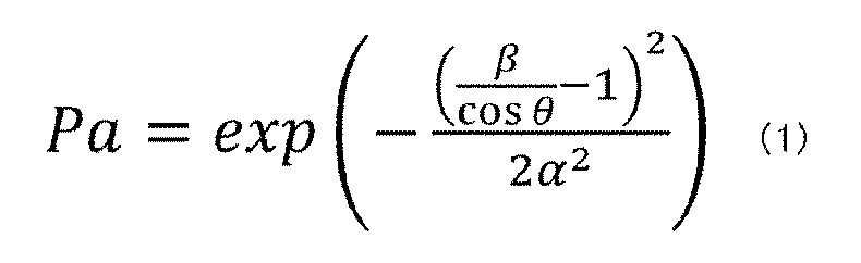
上記数式(1)において、θは、90度未満であり、かつ第1の絶縁層の第1の開口部における側面と、第1の導電層の上面のなす角度を表す。αは、0より大きい実数であり、かつ第1の元素の供給におけるイオンの投影飛程に対する標準偏差の比を表す。βは、0より大きい実数であり、かつ第1の導電層の上面に垂直な方向において、第2の絶縁層の第1の導電層の上面に沿って設けられる部分の厚さに対する、第2の絶縁層の第1の絶縁層の側面に沿って設けられる部分の厚さの比を表す。
前述の半導体装置の作製方法において、第1の元素を供給する前に、第2の絶縁層を介して、プラズマイオンドーピング法またはイオン注入法を用いて、半導体層に第2の元素を供給することが好ましい。第2の元素は、アルゴン、クリプトンまたはキセノンであることが好ましい。
本発明の一態様により、微細なサイズのトランジスタを有する半導体装置を提供できる。または、チャネル長の短いトランジスタを有する半導体装置を提供できる。または、オン電流の大きいトランジスタを有する半導体装置を提供できる。または、電界効果移動度の高いトランジスタを有する半導体装置を提供できる。または、電気特性が良好なトランジスタを有する半導体装置を提供できる。または、高速に動作する半導体装置を提供できる。または、占有面積の小さい半導体装置を提供できる。または、配線抵抗の低い半導体装置を提供できる。または、消費電力の低い半導体装置または表示装置を提供できる。または、信頼性の高いトランジスタ、半導体装置、または表示装置を提供できる。または、高精細の表示装置を提供できる。または、生産性の高い半導体装置または表示装置の作製方法を提供できる。または、新規なトランジスタ、半導体装置、表示装置、またはこれらの作製方法を提供できる。
なお、これらの効果の記載は、他の効果の存在を妨げるものではない。本発明の一態様は、必ずしも、これらの効果の全てを有する必要はない。明細書、図面、請求項の記載から、これら以外の効果を抽出することが可能である。
図1Aは、半導体装置の一例を示す上面図である。図1B及び図1Cは、半導体装置の一例を示す断面図である。
図2A乃至図2Dは、半導体装置の一例を示す斜視図である。
図3Aは、半導体装置の一例を示す上面図である。図3Bは、半導体装置の一例を示す断面図である。
図4は、半導体装置の一例を示す断面図である。
図5A及び図5Bは、不純物元素の濃度の一例を示す図である。
図6は、不純物元素の濃度の比の一例を示す図である。
図7は、半導体装置の一例を示す断面図である。
図8A及び図8Bは、不純物元素の濃度の比の一例を示す図である。
図9は、不純物元素の濃度の比の一例を示す図である。
図10は、半導体装置の一例を示す断面図である。
図11A乃至図11Dは、半導体装置の一例を示す断面図である。
図12は、半導体装置の一例を示す断面図である。
図13A乃至図13Cは、半導体装置の一例を示す断面図である。
図14A及び図14Bは、半導体装置の一例を示す断面図である。
図15A及び図15Bは、半導体装置の一例を示す断面図である。
図16A及び図16Bは、半導体装置の一例を示す断面図である。
図17A及び図17Bは、半導体装置の一例を示す断面図である。
図18は、半導体装置の一例を示す断面図である。
図19A及び図19Bは、半導体装置の一例を示す断面図である。
図20Aは、半導体装置の一例を示す上面図である。図20B及び図20Cは、半導体装置の一例を示す断面図である。
図21A乃至図21Iは、半導体装置の一例を示す回路図である。
図22Aは、半導体装置の一例を示す上面図である。図22B及び図22Cは、半導体装置の一例を示す断面図である。
図23Aは、半導体装置の一例を示す上面図である。図23B及び図23Cは、半導体装置の一例を示す断面図である。
図24Aは、半導体装置の一例を示す上面図である。図24Bは、半導体装置の一例を示す断面図である。
図25Aは、半導体装置の一例を示す上面図である。図25Bは、半導体装置の一例を示す断面図である。
図26A及び図26Bは、半導体装置の等価回路図である。図26Cは、半導体装置の一例を示す上面図である。
図27は、半導体装置の一例を示す断面図である。
図28は、半導体装置の一例を示す斜視図である。
図29A乃至図29Dは、半導体装置の一例を示す斜視図である。
図30A及び図30Bは、半導体装置の等価回路図である。図30Cは、半導体装置の一例を示す上面図である。
図31は、半導体装置の一例を示す断面図である。
図32は、半導体装置の一例を示す斜視図である。
図33A乃至図33Dは、半導体装置の一例を示す斜視図である。
図34A乃至図34Eは、半導体装置の作製方法の一例を示す断面図である。
図35A乃至図35Dは、半導体装置の作製方法の一例を示す断面図である。
図36A乃至図36Cは、半導体装置の作製方法の一例を示す断面図である。
図37は、半導体装置の作製方法の一例を示す断面図である。
図38A及び図38Bは、半導体装置の作製方法の一例を示す断面図である。
図39は、表示装置の一例を示す斜視図である。
図40A及び図40Bは、表示装置の一例を示す断面図である。
図41は、表示装置の一例を示す断面図である。
図42A乃至図42Cは、表示装置の一例を示す断面図である。
図43A及び図43Bは、表示装置の一例を示す断面図である。
図44は、表示装置の一例を示す断面図である。
図45は、表示装置の一例を示す断面図である。
図46は、表示装置の一例を示す断面図である。
図47A及び図47Bは、表示装置の一例を示す断面図である。
図48A乃至図48Dは、電子機器の一例を示す図である。
図49A乃至図49Fは、電子機器の一例を示す図である。
図50A乃至図50Gは、電子機器の一例を示す図である。
図2A乃至図2Dは、半導体装置の一例を示す斜視図である。
図3Aは、半導体装置の一例を示す上面図である。図3Bは、半導体装置の一例を示す断面図である。
図4は、半導体装置の一例を示す断面図である。
図5A及び図5Bは、不純物元素の濃度の一例を示す図である。
図6は、不純物元素の濃度の比の一例を示す図である。
図7は、半導体装置の一例を示す断面図である。
図8A及び図8Bは、不純物元素の濃度の比の一例を示す図である。
図9は、不純物元素の濃度の比の一例を示す図である。
図10は、半導体装置の一例を示す断面図である。
図11A乃至図11Dは、半導体装置の一例を示す断面図である。
図12は、半導体装置の一例を示す断面図である。
図13A乃至図13Cは、半導体装置の一例を示す断面図である。
図14A及び図14Bは、半導体装置の一例を示す断面図である。
図15A及び図15Bは、半導体装置の一例を示す断面図である。
図16A及び図16Bは、半導体装置の一例を示す断面図である。
図17A及び図17Bは、半導体装置の一例を示す断面図である。
図18は、半導体装置の一例を示す断面図である。
図19A及び図19Bは、半導体装置の一例を示す断面図である。
図20Aは、半導体装置の一例を示す上面図である。図20B及び図20Cは、半導体装置の一例を示す断面図である。
図21A乃至図21Iは、半導体装置の一例を示す回路図である。
図22Aは、半導体装置の一例を示す上面図である。図22B及び図22Cは、半導体装置の一例を示す断面図である。
図23Aは、半導体装置の一例を示す上面図である。図23B及び図23Cは、半導体装置の一例を示す断面図である。
図24Aは、半導体装置の一例を示す上面図である。図24Bは、半導体装置の一例を示す断面図である。
図25Aは、半導体装置の一例を示す上面図である。図25Bは、半導体装置の一例を示す断面図である。
図26A及び図26Bは、半導体装置の等価回路図である。図26Cは、半導体装置の一例を示す上面図である。
図27は、半導体装置の一例を示す断面図である。
図28は、半導体装置の一例を示す斜視図である。
図29A乃至図29Dは、半導体装置の一例を示す斜視図である。
図30A及び図30Bは、半導体装置の等価回路図である。図30Cは、半導体装置の一例を示す上面図である。
図31は、半導体装置の一例を示す断面図である。
図32は、半導体装置の一例を示す斜視図である。
図33A乃至図33Dは、半導体装置の一例を示す斜視図である。
図34A乃至図34Eは、半導体装置の作製方法の一例を示す断面図である。
図35A乃至図35Dは、半導体装置の作製方法の一例を示す断面図である。
図36A乃至図36Cは、半導体装置の作製方法の一例を示す断面図である。
図37は、半導体装置の作製方法の一例を示す断面図である。
図38A及び図38Bは、半導体装置の作製方法の一例を示す断面図である。
図39は、表示装置の一例を示す斜視図である。
図40A及び図40Bは、表示装置の一例を示す断面図である。
図41は、表示装置の一例を示す断面図である。
図42A乃至図42Cは、表示装置の一例を示す断面図である。
図43A及び図43Bは、表示装置の一例を示す断面図である。
図44は、表示装置の一例を示す断面図である。
図45は、表示装置の一例を示す断面図である。
図46は、表示装置の一例を示す断面図である。
図47A及び図47Bは、表示装置の一例を示す断面図である。
図48A乃至図48Dは、電子機器の一例を示す図である。
図49A乃至図49Fは、電子機器の一例を示す図である。
図50A乃至図50Gは、電子機器の一例を示す図である。
実施の形態について、図面を用いて詳細に説明する。但し、本発明は以下の説明に限定されず、本発明の趣旨及びその範囲から逸脱することなくその形態及び詳細を様々に変更し得ることは当業者であれば容易に理解される。従って、本発明は以下に示す実施の形態の記載内容に限定して解釈されるものではない。
なお、以下に説明する発明の構成において、同一部分または同様な機能を有する部分には同一の符号を異なる図面間で共通して用い、その繰り返しの説明は省略する。また、同様の機能を指す場合には、ハッチングパターンを同じくし、特に符号を付さない場合がある。
図面において示す各構成の、位置、大きさ、及び、範囲などは、理解の簡単のため、実際の位置、大きさ、及び、範囲などを表していない場合がある。このため、開示する発明は、必ずしも、図面に開示された位置、大きさ、及び、範囲などに限定されない。
なお、本明細書等において、「第1」、「第2」という序数詞は、便宜上用いるものであり、構成要素の数、または、構成要素の順序(例えば、工程順、または積層順)を限定するものではない。また、本明細書のある箇所において構成要素に付す序数詞と、本明細書の他の箇所、または特許請求の範囲において、当該構成要素に付す序数詞と、が一致しない場合がある。
なお、「膜」という言葉と、「層」という言葉とは、場合によっては、または、状況に応じて、互いに入れ替えることが可能である。例えば、「導電層」という用語を、「導電膜」という用語に変更することが可能である。または、例えば、「絶縁膜」という用語を、「絶縁層」という用語に変更することが可能である。
トランジスタは半導体素子の一種であり、電流または電圧を増幅する機能、及び、導通または非導通を制御するスイッチング動作などを実現することができる。本明細書におけるトランジスタは、IGFET(Insulated Gate Field Effect Transistor)及び薄膜トランジスタ(TFT:Thin Film Transistor)を含む。
「ソース」と「ドレイン」の機能は、異なる極性のトランジスタを採用する場合、または回路動作において電流の方向が変化する場合などには入れ替わることがある。このため、本明細書においては、「ソース」と「ドレイン」の用語は、入れ替えて用いることができるものとする。なお、トランジスタのソース及びドレインの呼称については、ソース端子及びドレイン端子、またはソース電極及びドレイン電極等、状況に応じて適切に言い換えることができる。
本明細書等において、「電気的に接続」には、「何らかの電気的作用を有するもの」を介して接続されている場合が含まれる。ここで、「何らかの電気的作用を有するもの」は、接続対象間での電気信号の授受を可能とするものであれば、特に制限を受けない。例えば、「何らかの電気的作用を有するもの」には、電極または配線をはじめ、トランジスタなどのスイッチング素子、抵抗素子、コイル、その他の各種機能を有する素子などが含まれる。
本明細書等において、特に断りがない場合、オフ電流とは、トランジスタがオフ状態(非導通状態、遮断状態、ともいう)にあるときのソース−ドレイン間のリーク電流をいう。オフ状態とは、特に断りがない場合、nチャネル型トランジスタでは、ゲートとソースの間の電圧Vgsがしきい値電圧Vthよりも低い(pチャネル型トランジスタでは、Vthよりも高い)状態をいう。
本明細書等において、構成要素の上面形状とは、上面視(平面視ともいう)における当該構成要素の輪郭形状を指す。また、上面視とは、当該構成要素の被形成面、または当該構成要素が形成される支持体(例えば、基板)の表面の法線方向から見ることを指す。
本明細書等において「上面形状が概略一致」とは、積層した層と層との間で少なくとも輪郭の一部が重なることをいう。例えば、上層と下層とが、同一のマスクパターン、または一部が同一のマスクパターンにより加工された場合を含む。ただし、厳密には輪郭が重なり合わず、上層が下層の内側に位置すること、または上層が下層の外側に位置することもあり、この場合も「上面形状が概略一致」という場合がある。また、上面形状が一致または概略一致している場合、端部が揃っている、または概略揃っているということもできる。
なお、本明細書等において、テーパ形状とは、構造の側面の少なくとも一部が、基板面または被形成面に対して傾斜して設けられている形状のことを指す。また、傾斜した側面と基板面または被形成面とがなす角を、テーパ角ということがある。なお、構造の側面、基板面、及び被形成面は、必ずしも完全に平坦である必要はなく、微小な曲率を有する略平面状、または微細な凹凸を有する略平面状であってもよい。
本明細書等において、メタルマスク、またはFMM(ファインメタルマスク、高精細なメタルマスク)を用いて作製されるデバイスをMM(メタルマスク)構造のデバイスと呼称する場合がある。また、本明細書等において、メタルマスク、またはFMMを用いずに作製されるデバイスをMML(メタルマスクレス)構造のデバイスと呼称する場合がある。なお、MML構造のデバイスは、メタルマスクを用いることなく製造することができるため、メタルマスクの合わせ精度に起因する精細度の上限を超えることができる。また、MML構造のデバイスは、メタルマスクの製造に係る設備およびメタルマスクの洗浄工程を不要にすることができる。また、MML構造のデバイスは、製造コストを低く抑えることが可能となるため、大量生産に適している。
本明細書等では、発光波長が異なる発光素子(発光デバイスともいう)で発光層を作り分ける構造をSBS(Side By Side)構造と呼ぶ場合がある。SBS構造は、発光素子ごとに材料及び構成を最適化することができるため、材料及び構成の選択の自由度が高まり、輝度の向上及び信頼性の向上を図ることが容易となる。
本明細書等において、正孔または電子を、「キャリア」といって示す場合がある。例えば、発光素子における正孔注入層または電子注入層を「キャリア注入層」といい、正孔輸送層または電子輸送層を「キャリア輸送層」といい、正孔ブロック層または電子ブロック層を「キャリアブロック層」という場合がある。なお、上述のキャリア注入層、キャリア輸送層、及びキャリアブロック層は、明確に区別できない場合がある。また、1つの層が、キャリア注入層、キャリア輸送層、及びキャリアブロック層のうち2つまたは3つの機能を兼ねる場合がある。
本明細書等において、発光素子は、一対の電極間にEL層を有する。EL層は、少なくとも発光層を有する。ここで、EL層が有する層(機能層ともいう)として、発光層、キャリア注入層(正孔注入層及び電子注入層)、キャリア輸送層(正孔輸送層及び電子輸送層)、及び、キャリアブロック層(正孔ブロック層及び電子ブロック層)などが挙げられる。本明細書等において、受光素子(受光デバイスともいう)は、一対の電極間に少なくとも光電変換層として機能する活性層を有する。本明細書等では、一対の電極の一方を画素電極と記し、他方を共通電極と記すことがある。
本明細書等において、犠牲層(マスク層と呼称してもよい)とは、少なくとも発光層(より具体的には、EL層を構成する層のうち、島状に加工される層)の上方に位置し、製造工程中において、当該発光層を保護する機能を有する。
本明細書等において、段切れとは、層、膜、または電極が、被形成面の形状(例えば段差など)に起因して分断される現象を示す。
(実施の形態1)
本実施の形態では、本発明の一態様の半導体装置について、図1A乃至図33Dを用いて説明する。
本実施の形態では、本発明の一態様の半導体装置について、図1A乃至図33Dを用いて説明する。
本発明の一態様は、半導体層と、第1の導電層と、第2の導電層と、第3の導電層と、第1の絶縁層と、第2の絶縁層と、を有する半導体装置である。第1の導電層は、トランジスタのソース電極及びドレイン電極の一方として機能し、第2の導電層は、他方として機能する。第3の導電層は、ゲート電極の一方として機能する。第2の絶縁層は、ゲート絶縁層として機能する。半導体層の第1の導電層と接する領域は、ソース領域及びドレイン領域の一方として機能し、第2の導電層と接する領域は、他方として機能する。
第1の絶縁層は、第1の導電層上に位置し、第1の導電層に達する第1の開口部を有する。第1の絶縁層の第1の開口部における側面と、第1の導電層の上面のなす角度は、66度以上90度以下である。第2の導電層は、第1の絶縁層上に位置し、第1の開口部と重なる領域に第2の開口部を有する。半導体層は、第1の開口部において、第1の導電層の上面と接する第1の領域と、第1の絶縁層の側面と接する第2の領域と、を有する。また、半導体層は、第2の開口部において、第2の導電層の側面と接する領域を有するとともに、第2の導電層の上面と接する第3の領域を有する。第2の絶縁層は、半導体層上に位置する。第3の導電層は、第2の絶縁層を介して、半導体層と重なる領域を有する。
第1の領域、第3の領域及び第2の絶縁層はそれぞれ、不純物元素を有する。不純物元素として、第1の元素を用いることが好ましい。第1の元素として、ホウ素、アルミニウム、インジウム、炭素、シリコン、ゲルマニウム、スズ、リン、ヒ素、アンチモン、マグネシウム、カルシウム、チタン、銅、亜鉛、タングステン、モリブデン、タンタル、ハフニウム、セリウム、及び貴ガス(ヘリウム、ネオン、アルゴン、クリプトン、キセノン等)のうち一種または複数種を用いることが好ましい。
第1の領域及び第3の領域が不純物元素を有することにより、ソース領域及びドレイン領域の電気抵抗を低くすることができ、オン電流の大きいトランジスタとすることができる。
第2の領域は、トランジスタのチャネル形成領域として機能する。第2の領域における第1の元素の濃度は、第1の領域における第1の元素の濃度の1×10⁻³倍以下であることが好ましい。第2の領域における第1の元素の濃度は、第3の領域における第1の元素の濃度の1×10⁻³倍以下であることが好ましい。第2の領域における第1の元素の濃度を低くすることにより、しきい値電圧がシフトすることを抑制でき、良好な電気特性を有するトランジスタとすることができる。
本発明の一態様のトランジスタは、ソース電極とドレイン電極とが、異なる高さに位置し、半導体層を流れる電流は、高さ方向に流れる。すなわち、チャネル長方向が高さ方向(縦方向)の成分を有するといえるため、本発明の一態様のトランジスタは、VFET(Vertical Field Effect Transistor)、縦型トランジスタ、縦型チャネルトランジスタ、縦チャネル型トランジスタなどとも呼ぶことができる。
本発明の一態様のトランジスタは、ソース電極、半導体層、及びドレイン電極を、重ねて設けることができるため、半導体層を平面状に配置した、いわゆるプレナー型のトランジスタと比較して、占有面積を大幅に縮小できる。
<構成例1>
〔構成例1−1〕
本発明の一態様である半導体装置について、説明する。半導体装置10の上面図(平面図ともいう)を、図1Aに示す。図1Aに示す一点鎖線A1−A2における切断面の断面図を図1Bに示し、一点鎖線B1−B2における切断面の断面図を図1Cに示す。なお、図1Aにおいて、半導体装置10の構成要素の一部(ゲート絶縁層等)を省略している。半導体装置の上面図については、以降の図面においても図1Aと同様に、構成要素の一部を省略する。半導体装置10の斜視図を、図2A乃至図2Dに示す。図2Bは、図2Aに示す一点鎖線C1−C2における切断面を示している。図2Cでは、図2Aに示す絶縁層を透過させ、輪郭を破線で示している。同様に、図2Dでは、図2Bに示す絶縁層を透過させ、輪郭を破線で示している。図1A及び図1Bの拡大図を、図3A及び図3Bに示す。
〔構成例1−1〕
本発明の一態様である半導体装置について、説明する。半導体装置10の上面図(平面図ともいう)を、図1Aに示す。図1Aに示す一点鎖線A1−A2における切断面の断面図を図1Bに示し、一点鎖線B1−B2における切断面の断面図を図1Cに示す。なお、図1Aにおいて、半導体装置10の構成要素の一部(ゲート絶縁層等)を省略している。半導体装置の上面図については、以降の図面においても図1Aと同様に、構成要素の一部を省略する。半導体装置10の斜視図を、図2A乃至図2Dに示す。図2Bは、図2Aに示す一点鎖線C1−C2における切断面を示している。図2Cでは、図2Aに示す絶縁層を透過させ、輪郭を破線で示している。同様に、図2Dでは、図2Bに示す絶縁層を透過させ、輪郭を破線で示している。図1A及び図1Bの拡大図を、図3A及び図3Bに示す。
半導体装置10は、トランジスタ100と、絶縁層110と、を有する。半導体装置10は、基板102上に設けられる。
トランジスタ100は、導電層104と、絶縁層106と、半導体層108と、導電層112aと、導電層112bと、を有する。導電層104は、ゲート電極として機能する。絶縁層106の一部は、ゲート絶縁層として機能する。導電層112aはソース電極及びドレイン電極の一方として機能し、導電層112bは他方として機能する。半導体層108のうち、ソース電極とドレイン電極との間において、ゲート絶縁層を介してゲート電極と重なる領域がチャネル形成領域として機能する。また、半導体層108のうち、ソース電極と接する領域はソース領域として機能し、ドレイン電極と接する領域はドレイン領域として機能する。
基板102上に導電層112aが設けられ、導電層112a上に絶縁層110が設けられ、絶縁層110上に導電層112bが設けられる。絶縁層110は、導電層112a及び導電層112bと接し、これらに挟持される領域を有する。導電層112aは、絶縁層110を介して導電層112bと重なる領域を有する。絶縁層110は、導電層112aに達する開口部141を有する。開口部141において、導電層112aが露出するともいえる。導電層112bは、導電層112aと重なる領域に開口部143を有する。開口部143は、開口部141と重なる領域に設けられる。
半導体層108は、開口部141及び開口部143を覆うように設けられる。半導体層108は、開口部141において導電層112aの上面と接する領域及び絶縁層110の側面と接する領域を有し、開口部143において導電層112bの側面と接する領域を有する。さらに、半導体層108は、導電層112bの上面と接する領域を有することが好ましい。半導体層108は、導電層112bの上面及び側面、絶縁層110の側面、並びに導電層112aの上面の形状に沿った形状を有する。
半導体層108に用いる半導体材料は、特に限定されない。例えば、単体元素よりなる半導体、または化合物半導体を用いることができる。単体元素よりなる半導体として、例えば、シリコン、及びゲルマニウムが挙げられる。化合物半導体として、例えば、ヒ化ガリウム、及びシリコンゲルマニウムが挙げられる。その他、化合物半導体として、例えば、有機半導体、窒化物半導体、及び酸化物半導体(OS:Oxide Semiconductor)が挙げられる。なお、これらの半導体材料に、ドーパントとして不純物が含まれてもよい。
半導体層108に用いる半導体材料の結晶性は特に限定されず、非晶質半導体、単結晶半導体、または単結晶以外の結晶性を有する半導体(微結晶半導体、多結晶半導体、または一部に結晶領域を有する半導体)のいずれを用いることができる。単結晶半導体または結晶性を有する半導体を用いると、トランジスタ特性の劣化を抑制できるため好ましい。
半導体層108は、例えば、シリコンを用いることができる。シリコンとして、単結晶シリコン、多結晶シリコン、微結晶シリコン、及び非晶質シリコンが挙げられる。多結晶シリコンとして、例えば、低温ポリシリコン(LTPS:Low Temperature Poly Silicon)が挙げられる。チャネル形成領域に非晶質シリコンを用いたトランジスタは、大型のガラス基板上に形成でき、低コストで作製することができる。チャネル形成領域に多結晶シリコンを用いたトランジスタは、電界効果移動度が高く、高速動作が可能である。また、チャネル形成領域に微結晶シリコンを用いたトランジスタは、非晶質シリコンを用いたトランジスタより電界効果移動度が高く、高速動作が可能である。
半導体層108は、半導体特性を示す金属酸化物(酸化物半導体ともいう)を有することが好ましい。酸化物半導体を用いたトランジスタ(以下、OSトランジスタと記す)は、非晶質シリコンを用いたトランジスタと比較して電界効果移動度が極めて高い。また、OSトランジスタは、オフ電流が著しく小さく、当該トランジスタと直列に接続された容量に蓄積した電荷を長期間に亘って保持することが可能である。また、OSトランジスタを適用することで、半導体装置の消費電力を低減することができる。
半導体層108は、その一部に領域108Daを有し、他の一部に領域108Dbを有する。領域108Da及び領域108Dbはそれぞれ、不純物元素を有する。領域108Da及び領域108Dbはそれぞれ、半導体層108の他の領域(例えば、チャネル形成領域)よりも不純物元素の濃度が高く、かつ、電気抵抗が低い領域(以下、低抵抗領域とも記す)である。半導体層108において、チャネル形成領域は、領域108Daと領域108Dbの間に位置する。
図1B、図1C及び図3Bは、半導体層108の導電層112aの上面と接する領域のうち、導電層112aの上面と導電層104の下面との間に位置する領域に、領域108Daが形成されている例を示す。領域108Daが形成される領域は、これに限られず、例えば、導電層112aの上面と接する領域全体に、領域108Daが形成される構成とすることができる。例えば、半導体層108に不純物元素が供給される際に、または不純物元素が供給された後の工程で加わる熱によって、不純物元素が拡散する場合がある。
図1B、図1C及び図3Bでは、半導体層108の導電層112bの上面と接する領域に、領域108Dbが形成されている例を示す。なお、領域108Dbは、半導体層108における、導電層112bの側面と接する領域にも設けられる構成とすることができる。また、領域108Dbは、半導体層108における、絶縁層110の側面と接する領域の一部にも設けられる構成とすることができる。
不純物元素として、第1の元素を用いることが好ましい。または、不純物元素として、第1の元素と、水素と、の双方を用いることが好ましい。
第1の元素として、ホウ素、アルミニウム、インジウム、炭素、シリコン、ゲルマニウム、スズ、リン、ヒ素、アンチモン、マグネシウム、カルシウム、チタン、銅、亜鉛、タングステン、モリブデン、タンタル、ハフニウム、セリウム、及び貴ガス(ヘリウム、ネオン、アルゴン、クリプトン、キセノン等)のうち一種または複数種を用いることが好ましい。
なお、第1の元素として、上記の元素に限られず、第一遷移元素(3d遷移元素、3d遷移金属)、第二遷移元素(4d遷移元素、4d遷移金属)、第三遷移元素(5d遷移元素、5d遷移金属)、アルカリ土類金属元素、及び、希土類元素に含まれる元素のうち、一種または複数種を用いることができる。
ソース領域及びドレイン領域に、第1の元素を供給する(第1の元素を添加する、または第1の元素を注入する、ということもできる)ことで、ソース領域及びドレイン領域に酸素欠損(VO:Oxygen Vacancy)が生じる。そして、当該酸素欠損(VO)に水素が入った欠陥(以下、VOHとも記す)によりキャリアが生成される。これにより、ソース領域及びドレイン領域の電気抵抗を低くすることができる。また、半導体層108の電気抵抗、半導体層108と導電層112aとの接触抵抗、及び、半導体層108と導電層112bとの接触抵抗をそれぞれ低くすることができる。したがって、トランジスタ100のオン電流を大きくすることができる。オン電流を大きくすることで、トランジスタ100の動作電圧を低くすることができる。これにより、半導体装置の消費電力の低減を図ることができる。
第1の元素として酸素と結合しやすい元素を用いる場合、第1の元素は半導体層108中の酸素を奪い、酸素と結合した状態で存在する。また、半導体層108中には酸素欠損(VO)が生じる。第1の元素として酸素と結合して安定になる元素を用いると、半導体層108中の第1の元素は酸化された状態で安定に存在するため、トランジスタ100の作製工程中に加わる熱などで脱離しにくく、電気抵抗を低く保つことができる。このことから、第1の元素として、少なくとも作製工程中の温度においてその酸化物が固体で存在しうる元素を用いることが好ましい。具体的には、好ましい第1の元素として、水素以外の典型非金属元素、典型金属元素、及び遷移元素(遷移金属)が挙げられ、特に好ましい第1の元素として、ホウ素、リン、マグネシウム、アルミニウム、及び、シリコンが挙げられる。
以上のことから、第1の元素の一つとして、ホウ素、リン、マグネシウム、アルミニウム、またはシリコンを用いることが好ましい。特に、第1の元素の一つとして、ホウ素またはリンを用いることが好ましい。
水素は、酸素欠損を生じさせる機能に加えて、酸素欠損と結合する機能も有するため、不純物元素として好適である。
不純物元素の供給には、プラズマイオンドーピング法またはイオン注入法を好適に用いることができる。これらの方法は、イオンの加速エネルギー及びドーズ量により、深さ方向の濃度プロファイルを高い精度で制御することができる。なお、原料ガスをイオン化し、当該イオンを質量分離して供給するイオン注入法を用いることで、特定の質量のイオンを供給でき、供給される不純物元素の純度を高めることができる。または、イオンを質量分離せずに供給するプラズマイオンドーピング法を用いることで、生産性を高めることができる。
第1の元素としてホウ素を用いる場合、原料ガスとして、例えば、BF3ガスを用いることができる。第1の元素としてリンを用いる場合、原料ガスとして、例えば、PH3ガスを用いることができる。また、これらのガスから生じたイオンを質量分離して供給することにより、特定の質量のイオンを領域108Da及び領域108Dbに供給でき、より好ましい。
不純物元素として、第1の元素と、水素と、の双方を用いることで、領域108Da及び領域108Dbそれぞれの電気抵抗を低くしやすく、かつ、電気抵抗が低い状態を保つことができる。
第1の元素と、水素と、の双方を供給する場合、原料ガスとして、第1の元素及び水素を含むガス(例えば、PH3ガス及びB2H6ガス)を用いることができる。または、原料ガスとして、第1の元素を含むガスと水素を有するガスとの混合ガスを用いることもできる。第1の元素及び水素を含む原料ガスを用いることにより、原料ガスから生じたイオンを質量分離せずに供給することができるため、生産性を高めることができ、好ましい。例えば、原料ガスとしてB2H6ガスを用いることで、不純物元素としてホウ素と水素を供給することができる。また、例えば、原料ガスとしてPH3ガスを用いることで、不純物元素としてリンと水素を供給することができる。
領域108Daは、不純物元素の濃度Naが1×10¹⁹atoms/cm3以上1×1023atoms/cm3以下、好ましくは5×1019atoms/cm3以上5×1022atoms/cm3以下、より好ましくは5×1019atoms/cm3以上5×1021atoms/cm3以下である部分を含むことが好ましい。例えば、第1の元素としてホウ素を用いる場合、領域108Daはホウ素の濃度Naが前述の範囲である部分を含むことが好ましい。
領域108Dbは、不純物元素の濃度Nbが1×10¹⁹atoms/cm3以上1×1023atoms/cm3以下、好ましくは5×1019atoms/cm3以上5×1022atoms/cm3以下、より好ましくは5×1019atoms/cm3以上5×1021atoms/cm3以下である部分を含むことが好ましい。例えば、第1の元素としてホウ素を用いる場合、領域108Dbはホウ素の濃度Nbが前述の範囲である部分を含むことが好ましい。
領域108Daが2種類以上の不純物元素を含む場合は、少なくとも1種類が上記の範囲であることが好ましい。また、それぞれの不純物元素の濃度が、上記の範囲であるとより好ましい。領域108Dbについても同様である。
なお、領域108Da及び領域108Dbに不純物元素を供給する際、半導体層108のチャネル形成領域にも不純物元素が供給される場合がある。または、作製工程中に加わる熱などにより、領域108Da及び領域108Dbそれぞれに含まれる不純物元素の一部がチャネル形成領域に拡散する場合がある。
半導体層108のチャネル形成領域における不純物元素の濃度Ncは、低いことが好ましい。濃度Ncは、領域108Daにおける不純物元素の濃度Naより低いことが好ましい。濃度Ncは、領域108Dbにおける不純物元素の濃度Nbより低いことが好ましい。これにより、チャネル形成領域のキャリア濃度が高くなることを抑制できる。ここで、チャネル形成領域のキャリア濃度が高いと、トランジスタのしきい値電圧がシフトし、ゲート電圧が0V時に流れるドレイン電流(以下、カットオフ電流とも記す)が大きくなってしまう場合がある。例えば、nチャネル型トランジスタの場合、しきい値電圧がマイナス側にシフトすることで、カットオフ電流が大きくなってしまう場合がある。チャネル形成領域のキャリア濃度が高くなることを抑制することにより、しきい値電圧がシフトすることが抑制され、カットオフ電流が小さいトランジスタとすることができる。したがって、消費電力の低い半導体装置とすることができる。
濃度Ncは、濃度Naの1×10⁻¹倍以下であることが好ましく、さらには1×10⁻²倍以下であることが好ましく、さらには1×10⁻³倍以下であることが好ましく、さらには1×10⁻⁴倍以下であることが好ましい。同様に、濃度Ncは、濃度Nbの1×10⁻¹倍以下であることが好ましく、さらには1×10⁻²倍以下であることが好ましく、さらには1×10⁻³倍以下であることが好ましく、さらには1×10⁻⁴倍以下であることが好ましい。これにより、小さいカットオフ電流と、大きいオン電流が両立したトランジスタとすることができる。したがって、低い消費電力と高い性能が両立した半導体装置とすることができる。
濃度Naに対する、濃度Ncの比Paは、数式(2)で表すことができる。濃度Nbに対する、濃度Ncの比Pbは、数式(3)で表すことができる。比Pa及び比Pbはそれぞれ無次元量であり、0より大きい実数である。
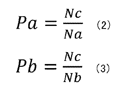
比Pa及び比Pbはそれぞれ、1×10⁻¹以下が好ましく、さらには1×10⁻²以下が好ましく、さらには1×10⁻³以下が好ましく、さらには1×10⁻⁴以下が好ましい。これにより、小さいカットオフ電流と、大きいオン電流が両立したトランジスタとすることができる。したがって、低い消費電力と高い性能が両立した半導体装置とすることができる。
半導体層108のチャネル形成領域、領域108Da、及び領域108Dbにおける不純物元素の濃度(ここでは、濃度Na、濃度Nb及び濃度Nc)の分析には、例えば、二次イオン質量分析法(SIMS:Secondary Ion Mass Spectrometry)、またはX線光電子分光法(XPS:X−ray Photoelectron Spectrometry、またはESCA:Electron Spectrometry for Chemical Analysis)を用いることができる。XPS分析を用いる場合には、試料の表面側または裏面側からのイオンスパッタリングとXPS分析を組み合わせることで、深さ方向の濃度分布を知ることができる。なお、前述したように、チャネル形成領域における濃度Ncは低いことが好ましい。したがって、濃度Ncは定量が困難となる、または検出下限未満となる場合がある。
本発明の一態様の半導体装置の作製において、チャネル形成領域と比較して、半導体層108のソース領域及びドレイン領域に不純物元素が供給されやすい方法を用いることが好ましい。不純物元素は、基板102の上面に対して垂直または概略垂直な方向から供給されることが好ましい。このとき、半導体層108において、基板102の上面に対して傾斜している領域は、基板102の上面に対して平行または概略平行な領域と比べて、供給される不純物元素の量が少なくなる。つまり、半導体層108のソース領域及びドレイン領域は、チャネル形成領域と比較して、供給される不純物元素の量が多くなる。したがって、優先的にソース領域及びドレイン領域の電気抵抗を低くすることができる。
絶縁層110として、無機絶縁層及び有機絶縁層の一方または双方を用いることができる。有機絶縁層に用いることができる材料として、例えば、アクリル樹脂、及びポリイミド樹脂が挙げられる。絶縁層110は、1層以上の無機絶縁層を有することが好ましい。無機絶縁層に用いることができる材料として、例えば、酸化物、窒化物、酸化窒化物、及び窒化酸化物が挙げられる。酸化物として、例えば、酸化シリコン、酸化アルミニウム、酸化マグネシウム、酸化ガリウム、酸化ゲルマニウム、酸化イットリウム、酸化ジルコニウム、酸化ランタン、酸化ネオジム、酸化ハフニウム、酸化タンタル、酸化セリウム、ガリウム亜鉛酸化物、及び、ハフニウムアルミネートが挙げられる。窒化物として、例えば、窒化シリコン、及び窒化アルミニウムが挙げられる。酸化窒化物として、例えば、酸化窒化シリコン、酸化窒化アルミニウム、酸化窒化ガリウム、酸化窒化イットリウム、及び、酸化窒化ハフニウムが挙げられる。窒化酸化物として、例えば、窒化酸化シリコン、及び窒化酸化アルミニウムが挙げられる。
なお、本明細書等において、酸化窒化物とは、その組成として窒素よりも酸素の含有量が多い材料を指す。窒化酸化物とは、その組成として酸素よりも窒素の含有量が多い材料を指す。
絶縁層110は、半導体層108と接する領域を有する。半導体層108に金属酸化物を用いる場合、半導体層108と絶縁層110との界面特性を向上させるため、絶縁層110の半導体層108と接する領域の少なくとも一部は酸素を有することが好ましい。具体的には、絶縁層110における半導体層108のチャネル形成領域と接する部分は、酸素を有することが好ましい。絶縁層110における半導体層108のチャネル形成領域と接する部分に、酸化物及び酸化窒化物の一以上を好適に用いることができる。
半導体層108に金属酸化物を用いる場合、絶縁層110の半導体層108と接する領域の少なくとも一部は加熱により酸素を放出することが好ましい。これにより、絶縁層110から半導体層108に酸素が供給され、半導体層108中の酸素欠損(VO)、及びVOHを低減することができる。
トランジスタ100のゲート絶縁層として機能する絶縁層106は、開口部141及び開口部143を覆うように設けられる。絶縁層106は、半導体層108、導電層112b、及び絶縁層110上に設けられる。絶縁層106は、半導体層108の上面及び側面、導電層112bの上面及び側面、並びに絶縁層110の上面と接する領域を有する。絶縁層106は、絶縁層110の上面、導電層112bの上面及び側面、半導体層108の上面及び側面、並びに導電層112aの上面の形状に沿った形状を有する。
図3Bでは、絶縁層106の領域108Daと接する部分の厚さTa、領域108Dbと接する部分の厚さTb、及びチャネル形成領域と接する部分の厚さTcを示している。厚さTa、厚さTb及び厚さTcはそれぞれ、絶縁層106の被形成面に垂直または概略垂直な方向における厚さである。より具体的には、厚さTaは、導電層112aの上面に沿って設けられる半導体層108の上面と、絶縁層106の上面との最短距離である。厚さTbは、導電層112bの上面に沿って設けられる半導体層108の上面と、絶縁層106の上面との最短距離である。厚さTcは、絶縁層110の側面に沿って設けられる半導体層108の絶縁層106側の側面と、絶縁層106の導電層104側の側面との最短距離である。図3Bでは、厚さTa、厚さTb及び厚さTcが互いに同じである構成を示しているが、本発明の一態様はこれに限られない。厚さTa、厚さTb及び厚さTcの一部または全てが異なる構成とすることもできる。
前述したように、絶縁層106の一部はゲート絶縁層として機能する。絶縁層106のチャネル形成領域と接する部分の厚さTcは、1nm以上200nm以下が好ましく、さらには1nm以上150nm以下が好ましく、さらには1nm以上100nm以下が好ましい。例えば、チャネル長が100nm以上500nm以下の場合、厚さTcは、30nm以上100nm以下が好ましい。また、例えば、チャネル長が10nm以上100nm以下の場合、厚さTcは、1nm以上50nm以下が好ましい。また、例えば、チャネル長が1nm以上10nm以下の場合、厚さTcは、1nm以上10nm以下が好ましい。
トランジスタ100のゲート電極として機能する導電層104は、絶縁層106上に設けられ、絶縁層106の上面と接する領域を有する。導電層104は、絶縁層106を介して、半導体層108と重なる領域を有する。導電層104は、絶縁層106の上面の形状に沿った形状を有する。
トランジスタ100は、半導体層108よりも上方にゲート電極を有する、いわゆるトップゲート型のトランジスタである。さらに、半導体層108の下面がソース電極及びドレイン電極と接することから、TGBC(Top Gate Bottom Contact)型のトランジスタということができる。また、トランジスタ100は、被形成面である基板102の表面に対してソース電極とドレイン電極とが異なる高さに位置し、基板102の表面に対して垂直方向、または概略垂直方向にドレイン電流が流れる。トランジスタ100において、縦方向、または概略縦方向にドレイン電流が流れるということもできる。そのため、本発明の一態様であるトランジスタは、VFETということができる。
トランジスタ100は、導電層112aと導電層112bの間に設けられる絶縁層110の厚さでチャネル長を制御することができる。したがって、トランジスタの作製に用いる露光装置の露光の最小寸法よりも短いチャネル長を有するトランジスタを精度高く作製できる。また、複数のトランジスタ100間の特性ばらつきも低減される。よって、半導体装置10の動作が安定し、信頼性を高めることができる。また、トランジスタの特性ばらつきが減ると、回路設計の自由度が高くなり、半導体装置の動作電圧を低くすることができる。よって、半導体装置の消費電力を低減できる。
本発明の一態様のトランジスタは、ソース電極、半導体層、及びドレイン電極を、重ねて設けることができるため、半導体層を平面状に配置した、いわゆるプレナー型のトランジスタと比較して、占有面積を大幅に縮小できる。
導電層112a、導電層112b、及び導電層104はそれぞれ、配線として機能することができ、トランジスタ100はこれらの配線が重なる領域に設けることができる。つまり、トランジスタ100及び配線を有する回路において、トランジスタ100及び配線の占有面積を縮小することができる。したがって、回路の占有面積を縮小することができ、小型の半導体装置とすることができる。
例えば、本発明の一態様の半導体装置を表示装置の画素回路に適用する場合、画素回路の占有面積を縮小することができ、高精細の表示装置とすることができる。また、例えば、本発明の一態様の半導体装置を表示装置の駆動回路(例えば、ゲート線駆動回路及びソース線駆動回路の一方または双方)に適用する場合、駆動回路の占有面積を縮小することができ、狭額縁の表示装置とすることができる。
絶縁層110は、積層構造を有することが好ましい。図1B等では、絶縁層110が、絶縁層110aと、絶縁層110a上の絶縁層110bと、絶縁層110b上の絶縁層110cと、を有する例を示している。絶縁層110a、絶縁層110b及び絶縁層110cはそれぞれ、絶縁層110の説明で挙げた材料を用いることができる。
半導体層108の絶縁層110bと接する領域は、チャネル形成領域として機能する。絶縁層110bは酸素を有することが好ましく、前述の酸化物及び酸化窒化物のいずれか一つまたは複数を用いることが好ましい。具体的には、絶縁層110bには、酸化シリコン及び酸化窒化シリコンの一方または双方を好適に用いることができる。
絶縁層110bには、加熱により酸素を放出する材料を用いるとより好ましい。半導体装置10の作製工程中に加わる熱により、絶縁層110bが酸素を放出することで、半導体層108に酸素を供給することができる。絶縁層110bから半導体層108、特に半導体層108のチャネル形成領域に酸素を供給することで、酸素欠損(VO)が修復され、酸素欠損(VO)を低減することができる。また、VOHを低減することができる。したがって、良好な電気特性を示し、かつ信頼性の高いトランジスタとすることができる。
例えば、酸素を含む雰囲気における加熱処理、または、酸素を含む雰囲気におけるプラズマ処理を行うことで、絶縁層110bに酸素を供給することができる。また、絶縁層110bの上面に、スパッタリング法により、酸素を含む雰囲気で膜を形成することで酸素を供給することができる。その後、当該膜を除去してもよい。なお、絶縁層110bに酸素を供給する方法については、実施の形態2で具体的に説明する。
絶縁層110bは、スパッタリング法、またはプラズマ化学気相堆積(PECVD:Plasma Enhanced Chemical Vapor Deposition)法などの成膜方法で形成することが好ましい。特に、成膜ガスに水素を含むガス(例えば、水素ガス及びアンモニアガス)を用いない方法で形成することで、水素の含有量の極めて少ない膜とすることができる。絶縁層110bは、スパッタリング法を特に好適に用いることができる。これにより、チャネル形成領域に水素が供給されることを抑制し、トランジスタ100の電気特性を安定にすることができる。
絶縁層110aは、絶縁層110bと導電層112aとの間に設けられる。絶縁層110cは、絶縁層110bと導電層112bの間に設けられる。絶縁層110a及び絶縁層110cはそれぞれ、自身から放出される不純物(例えば、水素及び水)の量が少ないことが好ましい。さらに、絶縁層110a及び絶縁層110cはそれぞれ、物質(例えば、原子、分子及びイオン)が透過しにくいことが好ましい。絶縁層110a及び絶縁層110cは、バリア膜として機能するともいえる。具体的には、絶縁層110a及び絶縁層110cはそれぞれ、不純物が透過しにくいことが好ましい。これにより、絶縁層110a及び絶縁層110cに含まれる不純物が、チャネル形成領域に拡散することを抑制できる。したがって、良好な電気特性を示し、かつ信頼性の高いトランジスタとすることができる。
絶縁層110a及び絶縁層110cはそれぞれ、酸素が透過しにくい材料を用いることが好ましい。これにより、絶縁層110bに含まれる酸素が、絶縁層110aを介して導電層112a側に拡散することを抑制できる。同様に、絶縁層110bに含まれる酸素が、絶縁層110cを介して導電層112b側に拡散することを抑制できる。これにより、絶縁層110bから半導体層108のチャネル形成領域へ供給される酸素の量が増え、チャネル形成領域の酸素欠損(VO)及びVOHを低減することができる。したがって、良好な電気特性を示し、かつ信頼性の高いトランジスタとすることができる。また、絶縁層110bに含まれる酸素によって導電層112aが酸化され、導電層112aの電気抵抗が高くなることを抑制できる。同様に、絶縁層110bに含まれる酸素によって導電層112bが酸化され、導電層112bの電気抵抗が高くなることを抑制できる。したがって、オン電流の大きいトランジスタとすることができる。
なお、本明細書等において、バリア膜とは、バリア性を有する膜を指す。バリア性とは、対象とする物質が拡散しづらく、それにより当該物質が膜を透過することを抑制する機能(透過性が低いともいう)、及び、当該物質を、捕獲、または固着する(ゲッタリングともいう)機能の一方または双方を指すものとする。例えば、バリア性を有する絶縁層を、バリア絶縁層ということができる。
バリア膜として機能する絶縁層110a及び絶縁層110cにはそれぞれ、例えば、アルミニウム及びハフニウムの一方または双方を有する酸化物、マグネシウムを有する酸化物、ガリウムを有する酸化物、シリコンを有する窒化物、及びシリコンを有する窒化酸化物の一または複数を用いることができる。具体的には、絶縁層110a及び絶縁層110cにはそれぞれ、例えば、酸化アルミニウム、酸化ハフニウム、ハフニウムアルミネート、酸化マグネシウム、酸化ガリウム、ガリウム亜鉛酸化物、窒化シリコン、及び窒化酸化シリコンの一または複数を好適に用いることができる。なお、絶縁層110aと絶縁層110cは同じ材料を用いることができる。または、絶縁層110aと絶縁層110cは異なる材料を用いることができる。
絶縁層110cに酸化物または酸化窒化物を用いることにより、絶縁層110c(または絶縁層110cとなる絶縁膜)を形成する際に、絶縁層110b(または絶縁層110bとなる絶縁膜)に酸素を供給することができる。
本明細書等において、異なる材料とは、構成元素の一部または全てが異なる材料、または構成元素が同じで組成が異なる材料をいう。
不純物元素は、絶縁層106を介して、半導体層108に供給されることが好ましい。絶縁層106を介して半導体層108に不純物元素を供給することで、供給の際に半導体層108に加わるダメージを軽減することができる。不純物元素の供給について、図4を用いて説明する。図4の下側に、絶縁層106を介して半導体層108に不純物元素を供給する際の絶縁層106、半導体層108及びその近傍の断面図を示す。ここでは、基板102の上面に対して垂直な方向から不純物元素が供給される例を挙げて、説明する。なお、図4に示す断面図では、絶縁層106の表面(具体的には、絶縁層106の上面及び側面)が、絶縁層106の被形成面である半導体層108の上面及び側面と平行である構成を示している。
図4では、不純物元素が供給される方向(ここでは、基板102の上面に対して垂直な方向)における、絶縁層106の絶縁層110の側面に沿って設けられている領域の厚さTdを示している。厚さTdとして、例えば、絶縁層110bの上面端部と下面端部の中間点から、不純物元素が供給される方向(ここでは、基板102の上面に対して垂直な方向)に延びる直線上の絶縁層106の厚さを用いることができる。厚さTdと比較して、導電層112aの上面に沿って設けられている領域の厚さTa、及び導電層112bの上面に沿って設けられている領域の厚さTbは薄い。これにより、半導体層108における、導電層112aの上面または導電層112bの上面に沿って設けられている領域は、絶縁層110の側面に沿って設けられている領域に比べて、供給される不純物元素の量が多くなる。このように、半導体層108のチャネル形成領域に不純物元素が供給されることを抑制し、優先的にソース領域及びドレイン領域の電気抵抗を低くすることができる。
絶縁層106の厚さが大きいほど、厚さTaと厚さTdの差、及び厚さTbと厚さTdとの差をそれぞれ大きくすることができる。したがって、半導体層108のチャネル形成領域に不純物元素が供給されることを抑制し、優先的にソース領域及びドレイン領域の電気抵抗を低くすることができる。一方で、トランジスタを微細化する、または、極めて短いチャネル長のトランジスタを作製するためには、オン電流の向上、短チャネル効果の抑制などの観点から、厚さTcは小さい方が好ましい。
不純物元素を、絶縁層106を介して半導体層108に供給する場合、絶縁層106も、不純物元素を有することがある。領域108Da及び領域108Dbはそれぞれ、絶縁層106よりも不純物元素の濃度が高い部分を有すると、領域108Da及び領域108Dbの電気抵抗をより低くできるため、好ましい。絶縁層106における不純物元素の濃度の分析については、半導体層108における不純物元素の濃度の分析に係る記載を参照できる。
絶縁層106は、酸素を含む絶縁層を有することが好ましい。不純物元素として酸素と結合しやすい元素を用いる場合、半導体層108と同様に絶縁層106においても、不純物元素は酸素と結合した状態で存在する。酸素と不純物元素とが結合して安定になることにより、不純物元素を含む領域では、熱が加わっても酸素が脱離しにくくなるため、酸素が他の層に拡散することを抑制できる。これにより、絶縁層106から領域108Da及び領域108Dbに酸素が供給されることを抑制しつつ、チャネル形成領域に酸素を効率的に供給することができる。したがって、領域108Da及び領域108Dbの電気抵抗が高くなることを防ぎつつ、チャネル形成領域の酸素欠損を低減できる。その結果、電気特性が良好で、信頼性の高いトランジスタを実現できる。
例えば、不純物元素としてホウ素を用いた場合、領域108Da、領域108Db及び絶縁層106に含まれるホウ素は酸素と結合した状態で存在しうる。このことは、例えば、XPS分析において、B2O3結合に起因するピークが観測されることで確認できる。また、XPS分析において、ホウ素元素が単体で存在する状態に起因するスペクトルピークが観測されない、またはバックグラウンド程度にまでピーク強度が極めて小さくなる。
不純物元素が絶縁層106を介して半導体層108に供給される場合、当該不純物元素は絶縁層106の表面から侵入し、絶縁層106を通過した後、絶縁層106と半導体層108の界面を介して、半導体層108に達する。このとき、不純物元素が供給される方向における絶縁層106の厚さは、不純物元素が絶縁層106の表面から半導体層108に達するまでの深さDともいえる。絶縁層106の各領域における深さDを、図4の上側に示す。当該図において、横軸は断面視における絶縁層106の位置を示し、縦軸は深さDを示す。絶縁層106の導電層112aの上面に沿って設けられている領域における深さDは、絶縁層106の厚さTaに相当する。絶縁層106の導電層112bの上面に沿って設けられている領域における深さDは、絶縁層106の厚さTbに相当する。絶縁層106の絶縁層110の側面に沿って設けられている領域における深さDは、厚さTdに相当する。なお、不純物元素が絶縁層106を介して半導体層108に供給される場合、絶縁層106及び半導体層108をそれぞれ、被注入層と記す場合がある。
図4の上側に示すように、絶縁層106の絶縁層110の側面に沿って設けられている領域における深さ“Td”は、導電層112aの上面に沿って設けられている領域における深さ“Ta”より深く、導電層112bの上面に沿って設けられている領域における深さ“Tb”より深い。なお、図中で示す領域Aにおいて、深さDは“Ta”と“Td”の間の値をとり、領域Bにおいて、深さDは“Tb”と“Td”の間の値をとる。つまり、領域A及び領域Bにおいて、深さDは“Td”より小さい値となる。
不純物元素の供給にプラズマイオンドーピング法またはイオン注入法を用いる場合、不純物元素の濃度はガウス分布で表すことができる。具体的には、深さxにおける不純物元素の濃度N(x)を数式(4)で表すことができる。濃度N(x)は、0より大きい実数である。

上記数式(4)において、Qはドーズ量であり、mは投影飛程(Projected Range、Rpとも記す)であり、sは深さ方向の標準偏差(△Rpとも記す)である。ドーズ量Q、投影飛程m及び標準偏差sはそれぞれ0より大きい実数である。なお、投影飛程mは、注入においてイオンが停止する深さの平均値であり、深さ“m”において不純物元素の濃度が最も高くなる。
投影飛程m、標準偏差s(分散s2)における不純物元素の濃度のガウス分布を、図5Aに示す。図5Aにおいて、横軸は深さDを線形スケールで示し、縦軸は濃度N(D)を対数スケールで示す。図5Aに示すように、投影飛程mにおける濃度N(m)が最も高くなり、図5Aでは“Nmax”と記している。
投影飛程m及び標準偏差sは、例えば、シミュレーションソフトを用いて算出することができる。当該シミュレーションソフトとして、例えば、TRIM(Transport of Ion in Matter)、及びSRIM(Stopping and Range of Ions in Matter)が挙げられる。これらは、モンテカルロ法によりイオン注入過程をシミュレーションするソフトである。シミュレーションのパラメータとして、供給される不純物元素の種類(具体的には、イオンの種類)、被注入層の組成及び膜密度、並びに加速エネルギーを用いることができる。例えば、供給する不純物元素の質量数が大きいと、投影飛程mが小さくなる。また、元素の種類によってイオン注入における阻止能の高さが異なるため、被注入層の組成によって投影飛程mが異なる。また、被注入層の膜密度が高いと、阻止能が高くなり、投影飛程mが小さくなる。したがって、被注入層(例えば、絶縁層106)に用いる材料によって、投影飛程mを異ならせることができる。なお、膜密度とは、単位体積あたりの質量を指す。また、加速エネルギーが高いと、投影飛程mが大きく、標準偏差sが大きくなる。
領域108Daにおける不純物元素の濃度Naは、深さ“Ta”における不純物元素の濃度となり、数式(5)で表すことができる。領域108Dbにおける不純物元素の濃度Nbは、深さ“Tb”における不純物元素の濃度となり、数式(6)で表すことができる。チャネル形成領域における不純物元素の濃度Ncは、深さ“Td”における不純物元素の濃度となり、数式(7)で表すことができる。濃度Na、濃度Nb及び濃度Ncはそれぞれ、0より大きい実数である。

領域108Daにおける不純物元素の濃度Naに対する、チャネル形成領域における不純物元素の濃度Ncの比Paは、数式(8)で表すことができる。領域108Dbにおける不純物元素の濃度Nbに対する、チャネル形成領域における不純物元素の濃度Ncの比Pbは、数式(9)で表すことができる。
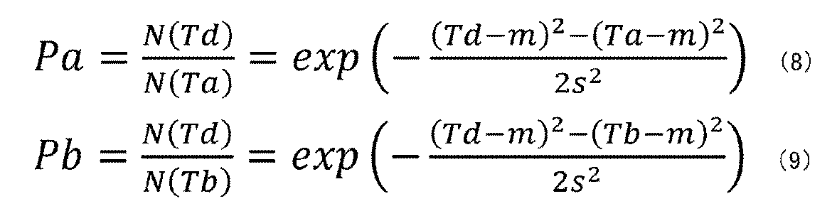
比Paは、数式(8)に示すように、厚さTa、厚さTd、投影飛程m及び標準偏差sで表すことができる。比Pbは、数式(9)に示すように、厚さTb、厚さTd、投影飛程m及び標準偏差sで表すことができる。比Pa及び比Pabそれぞれが前述の範囲となるように、厚さTa、厚さTb、厚さTd、投影飛程m及び標準偏差sを設定することが好ましい。数式(8)に示すように、厚さTdと厚さTaの差を大きくするほど比Paを小さくすることができる。数式(9)に示すように、厚さTdと厚さTbの差を大きくするほど比Pbを小さくすることができる。
ここで、絶縁層110の側面と絶縁層110の被形成面(ここでは、導電層112aの上面)とのなす角の角度θとすると、厚さTdは数式(10)で表すことができる。角度θが0度より大きく90度未満の場合、cosθは0より大きく1未満となる。したがって、厚さTdは厚さTcより厚くなる。また、角度θが小さいほど厚さTdが薄く、角度θが大きいほど厚さTdが厚くなる。つまり、角度θを大きくするほど、厚さTdと厚さTaの差を大きくすることができ、比Paを小さくすることができる。同様に、角度θを大きくするほど、厚さTdと厚さTbの差を大きくすることができ、比Pbを小さくすることができる。

角度θは、90度以下が好ましく、さらには90度未満であることが好ましい。角度θを小さくすることにより、絶縁層110上に設けられる層(例えば、半導体層108、絶縁層106及び導電層104)の被覆性を高めることができ、当該層に段切れまたは鬆といった不具合が発生することを抑制できる。
図4に示す断面図では、導電層112aの上面が、基板102の上面と平行である構成を示している。このとき、角度θは、絶縁層110の側面と基板102の上面とのなす角の角度と同じとなる。不純物元素は、導電層112aの上面に対して垂直または概略垂直な方向から供給されることが好ましい。つまり、不純物元素は、基板102の上面に対して垂直または概略垂直な方向から供給されることが好ましい。なお、断面視において、導電層112aの上面と基板102の上面が平行でない場合、不純物元素は、導電層112aの上面に対して垂直または概略垂直な方向から供給されることが好ましい。
厚さTdを数式(10)で表すとき、比Paは数式(11)で表すことができ、比Pbは数式(12)で表すことができる。

比Paは、数式(11)に示すように、角度θ、厚さTa、厚さTc、投影飛程m及び標準偏差sで表すことができる。比Pbは、数式(12)に示すように、角度θ、厚さTb、厚さTc、投影飛程m及び標準偏差sで表すことができる。比Pa及び比Pabそれぞれが前述の範囲となるように、角度θ、厚さTa、厚さTb、厚さTc、投影飛程m及び標準偏差sを設定することが好ましい。角度θが0度より大きく90度未満の場合、数式(11)及び数式(12)に示すように、角度θを大きくするほど比Pa及び比Pbを小さくすることができる。
ここで、導電層112aの上面に沿って設けられる領域の絶縁層106と半導体層108の界面、及び導電層112bの上面に沿って設けられる領域の絶縁層106と半導体層108の界面において、不純物元素の濃度N(D)が最も高くなるとする。また、厚さTa、厚さTb及び厚さTcが互いに同じとする。つまり、投影飛程mを“Ta”とすると、図5Bに示すように、深さ“Ta”における濃度Na、及び深さ“Tb”における濃度Nbが最も高くなる。また、厚さTdを“Ta/cosθ”で表すと、比Paは数式(13)で表すことができ、比Pbは数式(14)で表すことができる。

数式(13)及び数式(14)に示すように、比Pa及び比Pbはそれぞれ、角度θ、厚さTa及び標準偏差sで表すことができる。比Pa及び比Pabそれぞれが前述の範囲となるように、角度θ、厚さTa及び標準偏差sを設定することが好ましい。なお、厚さTaと厚さTbが互いに異なる場合は、数式(12)を用いることにより比Pbを算出することができる。
供給される不純物元素の種類、被注入層の組成、膜密度及び厚さに応じて加速エネルギーを選択することにより、投影飛程m及び標準偏差sが決まり、標準偏差sは数式(15)で表すことができる。αは投影飛程mに対する標準偏差sの比であり、無次元量である。また、αは0より大きい実数である。供給される不純物元素の種類、被注入層の組成、膜密度及び厚さに応じて加速エネルギーを選択することにより、比αは決まる。比αを用いて、比Paは数式(16)で表すことができ、比Pbは数式(17)で表すことができる。
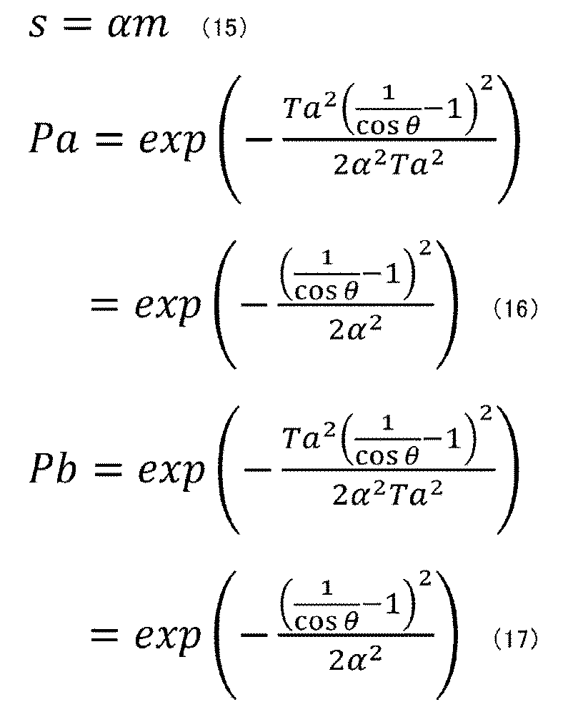
数式(16)及び数式(17)に示すように、比Pa及び比Pbはそれぞれ、角度θ、及び投影飛程mに対する標準偏差sの比αで表すことができる。比Pa及び比Pbそれぞれが前述の範囲となるように、比αに応じて角度θを設定することが好ましい。数式(16)及び数式(17)に示すように、比αが大きいほど、角度θを大きくすることにより、比Paを小さくすることができる。これにより、小さいカットオフ電流と、大きいオン電流が両立したトランジスタとすることができる。したがって、低い消費電力と高い性能が両立した半導体装置とすることができる。
角度θと比Paとの関係を、図6に示す。図6において、横軸は角度θを示し、縦軸は比Paを示す。図6では、比αを0.25、0.30、0.33、0.35、0.38、0.40、0.45、及び0.50で異ならせた場合の比Paを示している。
図6に示すように、比αが0.25以下の場合は角度θを59度以上、比αが0.30以下の場合は角度θを62度以上、比αが0.33以下の場合は角度θを64度以上、比αが0.35以下の場合は角度θを65度以上、比αが0.38以下の場合は角度θを66度以上、比αが0.40以下の場合は角度θを67度以上、比αが0.45以下の場合は角度θを69度以上、比αが0.50以下の場合は角度θを70度以上にすることにより、比Paを1×10⁻³以下とすることができ、好ましい。また、比αが0.25以下の場合は角度θを62度以上、比αが0.30以下の場合は角度θを65度以上、比αが0.33以下の場合は角度θを66度以上、比αが0.35以下の場合は角度θを67度以上、比αが0.38以下の場合は角度θを68度以上、比αが0.40以下の場合は角度θを69度以上、比αが0.45以下の場合は角度θを71度以上、比αが0.50以下の場合は角度θを72度以上にすることにより、比Paを1×10⁻⁴以下とすることができ、さらに好ましい。
以上のように、比αが大きいほど、角度θを大きくすることにより比Pa及び比Pbを小さくすることができる。
厚さTaと厚さTbが互いに同じ、または概略同じ場合、比Paと比Pbは互いに同じ、または概略同じとなるため、図6及び前述の記載における比Paを比Pbに置き換えることができる。
供給される不純物元素としてホウ素(具体的には、11B+イオン)、絶縁層106に膜密度が2.23g/cm3である酸化シリコン(SiO2)層を適用する構成を例に挙げて、より具体的に説明する。この構成のTRIMを用いたシミュレーションにおいて、加速エネルギーが20keVの場合、投影飛程mが約83.4nm、標準偏差sが約32.0nm(比αが約0.38)となる。比αを0.38としたとき、前述の数式(16)及び数式(17)から、角度θが65度で比Pa及び比Pbはそれぞれ1.6×10−3となり、角度θが66度で比Pa及び比Pbはそれぞれ6.3×10−4となり、角度θが68度で比Pa及び比Pbはそれぞれ6.4×10−5となる。したがって、角度θを66度以上にすることにより、比Pa及び比Pbをそれぞれ1×10−3以下とすることができ、角度θを68度以上にすることにより、比Pa及び比Pbをそれぞれ1×10−4以下とすることができる。
以上のように、角度θを大きくすることにより、比Pa及び比Pbを小さくすることができる。また、用いる不純物元素、及び絶縁層106の膜密度に応じて、角度θを大きくすることにより、比Pa及び比Pbを小さくすることができる。
ここでは、絶縁層106の厚さTa、厚さTb及び厚さTcが互いに同じ構成を例に挙げて説明したが、本発明の一態様はこれに限られない。厚さTa、厚さTb及び厚さTcの一部及び全てが異なる構成とすることもできる。図7は、厚さTcが厚さTa及び厚さTbより薄い構成を示している。
厚さTcは、厚さTaを用いて数式(18)で表すことができる。βは厚さTaに対する厚さTcの比であり、無次元量である。比βは0より大きい実数である。厚さTa及び厚さTcが互いに同じとき、比βは1である。

厚さTcが厚さTaと異なる、つまり数式(18)において比βが1ではない構成について、説明する。導電層112aの上面に沿って設けられる領域の絶縁層106の厚さTaと比較して、絶縁層110の側面に沿って設けられる領域の絶縁層106の厚さTcが薄くなる場合がある。このとき、比βは0より大きく1より小さい実数である。一方、厚さTaと比較して厚さTcが厚い場合、比βは1より大きい実数である。例えば、絶縁層106の形成にPECVD法またはスパッタリング法を用いる場合、厚さTcは厚さTaより薄く、つまり比βは1より小さくなる場合がある。絶縁層106の形成に原子層堆積(ALD:Atomic Layer Deposition)法を用いる場合、比βを1により近くすることができる。
厚さTcを数式(18)で表すとき、厚さTdは数式(19)で表すことができる。また、前述の数式(11)で示す比Paは、数式(20)で表すことができる。数式(12)で示す比Pbは、数式(21)で表すことができる。
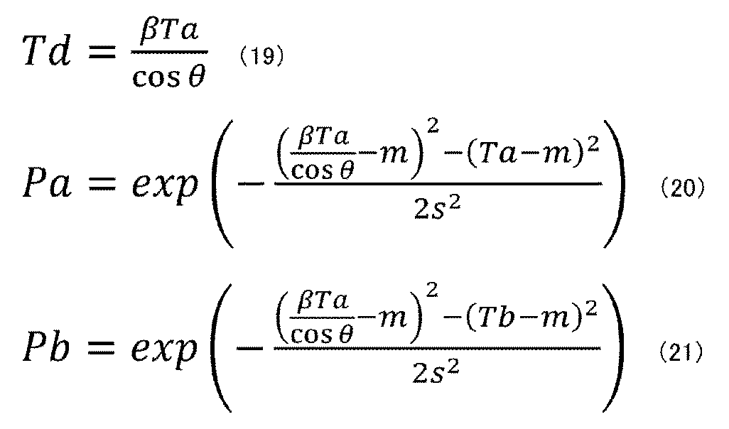
比Paは、数式(20)に示すように、比β、角度θ、厚さTa、投影飛程m及び標準偏差sで表すことができる。比Pbは、数式(21)に示すように、比β、厚さTa、厚さTb、投影飛程m及び標準偏差sで表すことができる。比Pa及び比Pabそれぞれが前述の範囲となるように、比βに応じて角度θ、厚さTa、厚さTb、投影飛程m及び標準偏差sを設定することが好ましい。数式(20)及び数式(21)に示すように、比βが小さいほど、角度θを大きくすることにより、比Paを小さくすることができる。これにより、小さいカットオフ電流と、大きいオン電流が両立したトランジスタとすることができる。したがって、低い消費電力と高い性能が両立した半導体装置とすることができる。
絶縁層106と半導体層108の界面における不純物元素の濃度Nが最も高くなるとする。また、厚さTa及び厚さTbが互いに同じとする。つまり、投影飛程mを“Ta”とすると、比Paは数式(22)で表すことができ、比Pbは数式(23)で表すことができる。

数式(22)及び数式(23)に示すように、比Pa及び比Pbはそれぞれ、比β、厚さTa、角度θ及び標準偏差sで表すことができる。比Pa及び比Pabそれぞれが前述の範囲となるように、比βに応じて角度θ、厚さTa及び標準偏差sを設定することが好ましい。
数式(15)に示すように標準偏差sを投影飛程m及び比αを用いて表し、投影飛程mを“Ta”とするとき、比Paは数式(24)で表すことができ、比Pbは数式(25)で表すことができる。

数式(24)及び数式(25)に示すように、比Pa及び比Pbはそれぞれ、投影飛程mに対する標準偏差sの比α、厚さTaに対する厚さTcの比β、及び角度θで表すことができる。比Pa及び比Pbそれぞれが前述の範囲となるように、比α及び比βに応じて角度θを設定することが好ましい。なお、数式(24)においてβを1とした場合の比Paが、前述の数式(16)である。数式(25)においてβを1とした場合の比Pbが、前述の数式(17)である。
角度θと比Paとの関係を、図8A及び図8Bに示す。図8Aは比βが0.85における角度θと比Paとの関係を示し、図8Bは比βが0.75における角度θと比Paとの関係を示す。図8A及び図8Bにおいて、横軸は角度θを示し、縦軸は比Paを示す。図8A及び図8Bではそれぞれ、比αを0.25、0.30、0.33、0.35、0.38、0.40、0.45、及び0.50で異ならせた場合の比Paを示している。なお、図6は、比βが1における角度θと比Paとの関係を示していることになる。
図8Aに示すように、比βが0.85において、比αが0.25以下の場合は角度θを64度以上、比αが0.30以下の場合は角度θを67度以上、比αが0.33以下の場合は角度θを68度以上、比αが0.35以下の場合は角度θを69度以上、比αが0.38以下の場合は角度θを70度以上、比αが0.40以下の場合は角度θを71度以上、比αが0.45以下の場合は角度θを72度以上、比αが0.50以下の場合は角度θを73度以上にすることにより、比Paを1×10⁻³以下とすることができ、好ましい。また、比αが0.25以下の場合は角度θを66度以上、比αが0.30以下の場合は角度θを69度以上、比αが0.33以下の場合は角度θを70度以上、比αが0.35以下の場合は角度θを71度以上、比αが0.38以下の場合は角度θを72度以上、比αが0.40以下の場合は角度θを72度以上、比αが0.45以下の場合は角度θを74度以上、比αが0.50以下の場合は角度θを75度以上にすることにより、比Paを1×10⁻⁴以下とすることができ、さらに好ましい。
図8Bに示すように、比βが0.75において、比αが0.25以下の場合は角度θを68度以上、比αが0.30以下の場合は角度θを70度以上、比αが0.33以下の場合は角度θを71度以上、比αが0.35以下の場合は角度θを71度以上、比αが0.38以下の場合は角度θを72度以上、比αが0.40以下の場合は角度θを73度以上、比αが0.45以下の場合は角度θを74度以上、比αが0.50以下の場合は角度θを75度以上にすることにより、比Paを1×10⁻³以下とすることができ、好ましい。また、比αが0.25以下の場合は角度θを69度以上、比αが0.30以下の場合は角度θを71度以上、比αが0.33以下の場合は角度θを72度以上、比αが0.35以下の場合は角度θを73度以上、比αが0.38以下の場合は角度θを74度以上、比αが0.40以下の場合は角度θを74度以上、比αが0.45以下の場合は角度θを76度以上、比αが0.50以下の場合は角度θを77度以上にすることにより、比Paを1×10⁻⁴以下とすることができ、さらに好ましい。
以上のように、比αが大きいほど、角度θを大きくすることにより、比Paを小さくすることができる。これにより、小さいカットオフ電流と、大きいオン電流が両立したトランジスタとすることができる。したがって、低い消費電力と高い性能が両立した半導体装置とすることができる。
厚さTaと厚さTbが互いに同じ、または概略同じ場合、比Paと比Pbは互いに同じ、または概略同じとなるため、図8A、図8B及び前述の記載における比Paを比Pbに置き換えることができる。
前述したように、絶縁層106の厚さTdと厚さTaの差が大きいことが好ましい。絶縁層106の厚さTdと厚さTbの差が大きいことが好ましい。つまり、厚さTaに対する厚さTdの比は、大きいことが好ましい。厚さTbに対する厚さTdの比は、大きいことが好ましい。
厚さTdを、厚さTaを用いて数式(26)で表すことができる。γは、厚さTaに対する厚さTdの比であり、無次元量である。また、比γは、0より大きい実数である。なお、比γは、数式(19)における“β/cosθ”にあたる。比γを用いて、比Paは数式(27)で表すことができる。また、絶縁層106の厚さTbと厚さTaが互いに同じとすると、比Pbは数式(28)で表すことができる。

数式(27)及び数式(28)に示すように、比Pa及び比Pbはそれぞれ、投影飛程mに対する標準偏差sの比α、及び絶縁層106の厚さTaに対する厚さTdの比γで表すことができる。比Pa及び比Pbそれぞれが前述の範囲となるように、比αに応じて比βを設定することが好ましい。数式(27)及び数式(28)に示すように、比γを大きくするほど、比Pa及び比Pbを小さくすることができる。つまり、厚さTaに対する厚さTdの比を大きくするほど、比Pa及び比Pbを小さくすることができる。
比γと比Paとの関係を、図9に示す。図9において、横軸は角度θを示し、縦軸は比Paを示す。図9では、比αを0.25、0.30、0.33、0.35、0.38、0.40、0.45、及び0.50で異ならせた場合の比Paを示している。
図9に示すように、比αが0.25以下の場合は比γを2.0以上、比αが0.30以下の場合は比γを2.2以上、比αが0.33以下の場合は比γを2.3以上、比αが0.35以下の場合は比γを2.4以上、比αが0.38以下の場合は比γを2.5以上、比αが0.40以下の場合は比γを2.5以上、比αが0.45以下の場合は比γを2.7以上、比αが0.50以下の場合は比γを2.9以上にすることにより、比Paを1×10⁻³以下とすることができ、好ましい。また、比αが0.25以下の場合は比γを2.1以上、比αが0.30以下の場合は比γを2.3以上、比αが0.33以下の場合は比γを2.5以上、比αが0.35以下の場合は比γを2.6以上、比αが0.38以下の場合は比γを2.7以上、比αが0.40以下の場合は比γを2.8以上、比αが0.45以下の場合は比γを3.0以上、比αが0.50以下の場合は比γを3.2以上にすることにより、比Paを1×10⁻⁴以下とすることができ、さらに好ましい。
以上のように、比αが大きいほど、比γを大きくすることにより、比Paを小さくすることができる。これにより、小さいカットオフ電流と、大きいオン電流が両立したトランジスタとすることができる。したがって、低い消費電力と高い性能が両立した半導体装置とすることができる。
厚さTaと厚さTbが互いに同じ、または概略同じ場合、比Paと比Pbは互いに同じ、または概略同じとなるため、図9及び前述の記載における比Paを比Pbに置き換えることができる。
供給される不純物元素としてホウ素(具体的には、11B+イオン)、絶縁層106に膜密度が2.23g/cm3である酸化シリコン(SiO2)層を適用する構成を例に挙げて、より具体的に説明する。この構成のTRIMを用いたシミュレーションにおいて、加速エネルギーが20keVの場合、投影飛程mが約83.4nm、標準偏差sが約32.0nm(比αが約0.38)となる。比αを0.38としたとき、前述の数式(27)及び数式(28)から、比γが2.4で比Pa及び比Pbはそれぞれ1.1×10−3となり、比γが2.5で比Pa及び比Pbはそれぞれ4.1×10−4となり、比γが2.6で比Pa及び比Pbはそれぞれ1.4×10−4となり、比γが2.7で比Pa及び比Pbはそれぞれ4.5×10−5となる。したがって、比γを2.5以上にすることにより、比Pa及び比Pbをそれぞれ1×10−3以下とすることができ、比γを2.7度以上にすることにより、比Pa及び比Pbをそれぞれ1×10−4以下とすることができる。
以上のように、比γを大きくすることにより、比Pa及び比Pbを小さくすることができる。また、用いる不純物元素、及び絶縁層106の膜密度に応じて、比γを大きくすることにより、比Pa及び比Pbを小さくすることができる。
前述したように、チャネル形成領域に供給される不純物元素の量は少ないことが好ましい。より具体的には、半導体層108の絶縁層110bと接する領域に供給される不純物元素の量は少ないことが好ましい。したがって、断面視において、絶縁層110bの上面端部から、不純物元素が供給される方向(ここでは、基板102の上面に対して垂直な方向)に延びる直線上の絶縁層106の厚さTeは、厚いことがより好ましい。厚さTeは、少なくとも厚さTdと同じ、または概略同じであることがより好ましい。
図4及び図7では、半導体層108の導電層112aの上面に沿って設けられる領域の厚さHa、導電層112bの上面に沿って設けられる領域の厚さHb、及び絶縁層110の側面に沿って設けられる領域の厚さHcを示している。厚さHa、厚さHb及び厚さHcはそれぞれ、半導体層108の被形成面に垂直または概略垂直な方向における厚さである。より具体的には、厚さHaは、導電層112aの上面と、半導体層108の上面との最短距離である。厚さHbは、導電層112bの上面と、半導体層108の上面との最短距離である。厚さHcは、絶縁層110の側面と半導体層108の絶縁層106側の側面との最短距離である。図4及び図7では、厚さHa、厚さHb及び厚さHcが互いに同じである構成を示しているが、本発明の一態様はこれに限られない。厚さHa、厚さHb及び厚さHcの一部または全てが異なる構成とすることもできる。
数式(29)に示すように、絶縁層110bの上面に沿って設けられる絶縁層106の厚さTb、半導体層108の厚さHb、導電層112bの厚さT112b、及び絶縁層110cの厚さT110cの和をKとする。和Kは、不純物元素が供給される方向(ここでは、基板102の上面に対して垂直な方向)における、導電層112bの上面に沿って設けられる絶縁層106の上面と、絶縁層110bの上面との距離である。和Kが薄いと、絶縁層106の厚さTeが厚さTdより薄くなる場合がある(図4または図7の領域B参照)。したがって、和Kは厚いことが好ましい。また、数式(30)に示すように、半導体層108の厚さHd、及び絶縁層106の厚さTdの和をLとする。数式(31)に示すように、和Kは、和L以上であることが好ましい。これにより、絶縁層106の厚さTeを厚くすることができる。
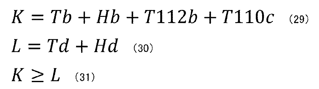
数式(31)を満たすように、絶縁層106の厚さTb及び厚さTd、半導体層108の厚さHb及び厚さHd、導電層112bの厚さT112b、及び絶縁層110cの厚さT110cを設定することが好ましい。例えば、数式(31)を満たすように、導電層112bの厚さT112b、及び絶縁層110cの厚さT110cの一方または双方を厚くすることが好ましい。
ここで、絶縁層106の厚さTbと厚さTcが互いに同じとすると、厚さTdは数式(32)で表すことができる。半導体層108の厚さHbと厚さHcが互いに同じとすると、厚さHdは数式(33)で表すことができる。また、和Lは、数式(34)で表すことができる。

数式(29)及び数式(34)を用いて、数式(31)を展開すると、数式(35)が得られる。

数式(35)に示すように、角度θが0度より大きく90度未満の場合、角度θが大きくなるほど、導電層112bの厚さT112bと絶縁層110cの厚さT110cの和を大きくすることが好ましい。具体的には、角度θが大きくなるほど、導電層112bの厚さT112b及び絶縁層110cの厚さT110cの一方または双方を厚くすることが好ましい。
例えば、角度θが60度以下の場合、導電層112bの厚さT112bと絶縁層110cの厚さT110cの和は、少なくとも絶縁層106の厚さTbと半導体層108の厚さHbの和以上であることがより好ましい。角度θが65度以下の場合、導電層112bの厚さT112bと絶縁層110cの厚さT110cの和は、少なくとも絶縁層106の厚さTbと半導体層108の厚さHbの和の1.4倍以上であることがより好ましい。角度θが70度以下の場合、導電層112bの厚さT112bと絶縁層110cの厚さT110cの和は、少なくとも絶縁層106の厚さTbと半導体層108の厚さHbの和の2.0倍以上であることがより好ましい。角度θが75度以下の場合、導電層112bの厚さT112bと絶縁層110cの厚さT110cの和は、少なくとも絶縁層106の厚さTbと半導体層108の厚さHbの和の2.9倍以上であることがより好ましい。角度θが80度以下の場合、導電層112bの厚さT112bと絶縁層110cの厚さT110cの和は、少なくとも絶縁層106の厚さTbと半導体層108の厚さHbの和の4.8倍以上であることがより好ましい。
なお、ここでは絶縁層106の厚さTbと厚さTcが互いに同じであり、半導体層108の厚さHbと厚さHcが互いに同じである構成を例に挙げて説明したが、本発明の一態様はこれに限られない。厚さTbと厚さTcが互いに異なる構成とすることもできる。厚さHbと厚さHcが互いに異なる構成とすることもできる。このような場合においても、数式(31)を満たすように各層の厚さを設定することが好ましい。
絶縁層106の厚さTcが厚さTbの0.85倍であり、半導体層108の厚さHcが厚さHbの0.85倍である場合を例に挙げて、説明する。この構成において、和Lは“0.85×(Tb+Hb)/cosθ”と表すことができ、これを数式(31)に適用することができる。例えば、角度θが60度以下の場合、導電層112bの厚さT112bと絶縁層110cの厚さT110cの和は、少なくとも絶縁層106の厚さTbと半導体層108の厚さHbの和の0.7倍以上であることがより好ましい。角度θが65度以下の場合、導電層112bの厚さT112bと絶縁層110cの厚さT110cの和は、少なくとも絶縁層106の厚さTbと半導体層108の厚さHbの和の1.1倍以上であることがより好ましい。角度θが70度以下の場合、導電層112bの厚さT112bと絶縁層110cの厚さT110cの和は、少なくとも絶縁層106の厚さTbと半導体層108の厚さHbの和の1.5倍以上であることがより好ましい。角度θが75度以下の場合、導電層112bの厚さT112bと絶縁層110cの厚さT110cの和は、少なくとも絶縁層106の厚さTbと半導体層108の厚さHbの和の2.3倍以上であることがより好ましい。角度θが80度以下の場合、導電層112bの厚さT112bと絶縁層110cの厚さT110cの和は、少なくとも絶縁層106の厚さTbと半導体層108の厚さHbの和の3.9倍以上であることがより好ましい。
前述したように、不純物元素の濃度の比Pa及び比Pbはそれぞれ小さいことが好ましい。比Pa及び比Pbそれぞれが前述の範囲となるように、角度θを決めることができる。さらに、当該角度θにおいて、数式(31)を満たすように、導電層112bの厚さT112bと絶縁層110cの厚さT110cの和を決めることがさらに好ましい。これにより、チャネル形成領域全体の不純物元素の濃度を低くすることができる。
領域108Da及び領域108Dbはそれぞれ、不純物元素として第1の元素に加えて、第2の元素を有する構成とすることができる。なお、第2の元素は、第1の元素と異なる。第2の元素として、前述の第1の元素として用いることができる元素のうち一種または複数種を用いることができる。第2の元素は、第1の元素より質量数が大きいことが好ましい。また、第1の元素は酸素と結合しやすいことが好ましい。例えば、第1の元素として、ホウ素またはリンを用い、第2の元素として、アルゴン、クリプトンまたはキセノンを用いることができる。
第2の元素を半導体層108に供給した後に、第1の元素を半導体層108に供給することができる。供給される元素の質量数が大きいと、半導体層108が有する金属酸化物において切断される金属と酸素の結合が多くなる。また、金属と酸素の結合の切断により、領域108Daとなる領域に及び領域108Dbとなる領域に酸素欠損(VO)が生じる。質量数の大きい第2の元素の供給でより多くの金属と酸素の結合を切断した後に、第1の元素を供給することにより、第1の元素は効率的に酸素と結合することができる。したがって、領域108Da及び領域108Dbの電気抵抗を効率的に低くすることができる。
チャネル形成領域に供給される第2の元素の量が多くなると、チャネル形成領域に酸素欠損(VO)が生じることによりVOHが増加し、キャリア濃度が高くなってしまう恐れがある。チャネル形成領域における第2の元素の濃度は、領域108Daにおける第2の元素の濃度より低いことが好ましい。同様に、チャネル形成領域における第2の元素の濃度は、領域108Dbにおける第2の元素の濃度より低いことが好ましい。
第2の元素は、絶縁層106を介して、半導体層108に供給されることが好ましい。絶縁層106を介して第2の元素を半導体層108に供給した後に、絶縁層106を介して第1の元素を半導体層108に供給することが好ましい。第2の元素を、絶縁層106を介して半導体層108に供給する場合、絶縁層106も、第2の不純物元素を有することがある。
第2の元素は、基板102の上面に対して垂直または概略垂直な方向から供給されることが好ましい。第2の元素の供給は、第1の元素の供給に用いることができる方法を用いることができる。第2の元素の供給は、例えば、プラズマイオンドーピング法またはイオン注入法を好適に用いることができる。第1の元素及び第2の元素の供給にプラズマイオンドーピング法またはイオン注入法を用いる場合、絶縁層110の角度θ、または絶縁層106の厚さTdを前述の範囲とすることにより、チャネル形成領域に供給される第2の元素の量を少なくすることができ、好ましい。なお、第1の元素と比較して第2の元素は質量数が大きいため、第1の元素を供給する際の加速エネルギーより、第2の元素を供給する際の加速エネルギーが高いとより好ましい。これにより、領域108Da及び領域108Dbに供給される第2の元素の量が多くなり、領域108Da及び領域108Dbの電気抵抗を効率的に低くすることができる。
または、第1の元素と第2の元素を同じ工程で供給することができる。例えば、第1の元素と、第2の元素とを含む原料ガスを用いて、第1の元素及び第2の元素を半導体層108に供給することができる。供給には、プラズマイオンドーピング法を好適に用いることができる。このとき、加速エネルギーは、第1の元素の濃度の比Pa及び比Pbが前述の範囲となるように設定することが好ましい。また、原料ガスとして、第1の元素を含むガスと、第2の元素を含むガスとの混合ガスを用いることができる。例えば、第1の元素をホウ素、第2の元素をアルゴンとする場合、BF3ガスとArガスの混合ガスを用いることができる。なお、混合ガスに限定されず、第1の元素と第2の元素とを含むガスを原料ガスとして用いることもできる。
なお、図1B等では、半導体層108、絶縁層106及び導電層104が開口部141及び開口部143を覆う例を示しているが、本発明の一態様はこれに限られない。絶縁層110及び導電層112bと、導電層112aとによって段差が形成され、当該段差に沿って半導体層108、絶縁層106及び導電層104が設けられる構成とすることができる。
[半導体層108]
半導体層108に用いることができる金属酸化物について、具体的に説明する。金属酸化物として、例えば、インジウム酸化物、ガリウム酸化物、及び亜鉛酸化物が挙げられる。金属酸化物は、少なくともインジウムまたは亜鉛を含むことが好ましい。また、金属酸化物は、インジウムと、元素Mと、亜鉛と、の中から選ばれる一または二以上を有することが好ましい。なお、元素Mは、酸素との結合エネルギーが高い金属元素または半金属元素であり、例えば、酸素との結合エネルギーがインジウムよりも高い金属元素または半金属元素である。元素Mとして、具体的には、アルミニウム、ガリウム、スズ、イットリウム、チタン、バナジウム、クロム、マンガン、鉄、コバルト、ニッケル、ジルコニウム、モリブデン、ハフニウム、タンタル、タングステン、ランタン、セリウム、ネオジム、マグネシウム、カルシウム、ストロンチウム、バリウム、ホウ素、シリコン、ゲルマニウム、及びアンチモンが挙げられる。金属酸化物が有する元素Mは、上記元素のいずれか一種または複数種であることが好ましく、ガリウム、アルミニウム、スズ、及びイットリウムから選ばれた一種または複数種であることがより好ましく、ガリウム、アルミニウム、及びスズの一種または複数種がさらに好ましい。これらの元素は、酸素との結合エネルギーが高い上、インジウムまたは亜鉛とイオン半径が同程度であるため、より好ましい。また、スズは4価であることから、キャリア移動度を高めることができ、より好ましい。なお、本明細書等において、金属元素と半金属元素をまとめて「金属元素」と呼ぶことがあり、本明細書等に記載の「金属元素」には半金属元素が含まれることがある。
半導体層108に用いることができる金属酸化物について、具体的に説明する。金属酸化物として、例えば、インジウム酸化物、ガリウム酸化物、及び亜鉛酸化物が挙げられる。金属酸化物は、少なくともインジウムまたは亜鉛を含むことが好ましい。また、金属酸化物は、インジウムと、元素Mと、亜鉛と、の中から選ばれる一または二以上を有することが好ましい。なお、元素Mは、酸素との結合エネルギーが高い金属元素または半金属元素であり、例えば、酸素との結合エネルギーがインジウムよりも高い金属元素または半金属元素である。元素Mとして、具体的には、アルミニウム、ガリウム、スズ、イットリウム、チタン、バナジウム、クロム、マンガン、鉄、コバルト、ニッケル、ジルコニウム、モリブデン、ハフニウム、タンタル、タングステン、ランタン、セリウム、ネオジム、マグネシウム、カルシウム、ストロンチウム、バリウム、ホウ素、シリコン、ゲルマニウム、及びアンチモンが挙げられる。金属酸化物が有する元素Mは、上記元素のいずれか一種または複数種であることが好ましく、ガリウム、アルミニウム、スズ、及びイットリウムから選ばれた一種または複数種であることがより好ましく、ガリウム、アルミニウム、及びスズの一種または複数種がさらに好ましい。これらの元素は、酸素との結合エネルギーが高い上、インジウムまたは亜鉛とイオン半径が同程度であるため、より好ましい。また、スズは4価であることから、キャリア移動度を高めることができ、より好ましい。なお、本明細書等において、金属元素と半金属元素をまとめて「金属元素」と呼ぶことがあり、本明細書等に記載の「金属元素」には半金属元素が含まれることがある。
半導体層108は、例えば、インジウム亜鉛酸化物(In−Zn酸化物、IZO(登録商標)とも記す)、インジウムスズ酸化物(In−Sn酸化物、ITOとも記す)、インジウムチタン酸化物(In−Ti酸化物)、インジウムガリウム酸化物(In−Ga酸化物)、インジウムタングステン酸化物(In−W酸化物、IWOとも記す)、インジウムガリウムアルミニウム酸化物(In−Ga−Al酸化物)、インジウムガリウムスズ酸化物(In−Ga−Sn酸化物、IGTOとも記す)、ガリウム亜鉛酸化物(Ga−Zn酸化物、GZOとも記す)、アルミニウム亜鉛酸化物(Al−Zn酸化物、AZOとも記す)、インジウムアルミニウム亜鉛酸化物(In−Al−Zn酸化物、IAZOとも記す)、インジウムスズ亜鉛酸化物(In−Sn−Zn酸化物、ITZO(登録商標)とも記す)、インジウムチタン亜鉛酸化物(In−Ti−Zn酸化物)、インジウムガリウム亜鉛酸化物(In−Ga−Zn酸化物、IGZOとも記す)、インジウムガリウムスズ亜鉛酸化物(In−Ga−Sn−Zn酸化物、IGZTOとも記す)、インジウムガリウムアルミニウム亜鉛酸化物(In−Ga−Al−Zn酸化物、IGAZO、IGZAO、またはIAGZOとも記す)などを用いることができる。または、シリコンを含むインジウムスズ酸化物(ITSOとも記す)、ガリウムスズ酸化物(Ga−Sn酸化物)、アルミニウムスズ酸化物(Al−Sn酸化物)などを用いることができる。
なお、金属酸化物は、インジウムに代えて、または、インジウムに加えて、元素周期表における周期番号が大きい金属元素の一種または複数種を有する構成とすることができる。金属元素の軌道の重なりが大きいほど、金属酸化物におけるキャリア伝導は大きくなる傾向がある。よって、周期番号が大きい金属元素を有することで、トランジスタの電界効果移動度を高めることができる場合がある。周期番号が大きい金属元素として、第5周期に属する金属元素、及び第6周期に属する金属元素などが挙げられる。当該金属元素として、具体的には、イットリウム、ジルコニウム、銀、カドミウム、スズ、アンチモン、バリウム、鉛、ビスマス、ランタン、セリウム、プラセオジム、ネオジム、プロメチウム、サマリウム、及びユウロピウムなどが挙げられる。なお、ランタン、セリウム、プラセオジム、ネオジム、プロメチウム、サマリウム、及びユウロピウムは、軽希土類元素と呼ばれる。
金属酸化物に含まれる全ての金属元素の原子数の和に対するインジウムの原子数の割合を高くすることにより、トランジスタの電界効果移動度を高めることができる。また、オン電流が大きいトランジスタを実現できる。
本明細書等において、含有される全ての金属元素の原子数の和に対するインジウムの原子数の割合を、インジウムの含有率と記す場合がある。他の金属元素においても同様である。元素Mとして複数の元素を有する場合は、含有される全ての金属元素の原子数の和に対する元素Mの原子数の割合の和を、元素Mの含有率とすることができる。
金属酸化物における亜鉛の含有率を高くすることにより、結晶性の高い金属酸化物となり、金属酸化物中の不純物の拡散を抑制できる。したがって、トランジスタの電気特性の変動が抑制され、信頼性を高めることができる。
金属酸化物における元素Mの含有率を高くすることにより、バンドギャップの大きい金属酸化物とすることができる。また、金属酸化物に酸素欠損(VO)が形成されることが抑制されることにより、酸素欠損(VO)に起因するキャリア生成が抑制され、トランジスタのしきい値電圧がシフトすることを抑制できる。これにより、カットオフ電流を小さくすることができ、ノーマリオフのトランジスタとすることができる。また、オフ電流が小さいトランジスタとすることができる。また、トランジスタの電気特性の変動が抑制され、信頼性を高めることができる。
半導体層108に適用する金属酸化物の組成により、トランジスタの電気特性、及び信頼性が異なる。したがって、トランジスタに求められる電気特性、及び信頼性に応じて金属酸化物の組成を異ならせることにより、優れた電気特性と高い信頼性を両立した半導体装置とすることができる。
金属酸化物がIn−M−Zn酸化物の場合、当該In−M−Zn酸化物におけるInの原子数比は元素Mの原子数比以上であることが好ましい。このようなIn−M−Zn酸化物の金属元素の原子数比として、例えば、In:M:Zn=1:1:1、In:M:Zn=1:1:1.2、In:M:Zn=2:1:3、In:M:Zn=3:1:1、In:M:Zn=3:1:2、In:M:Zn=4:2:3、In:M:Zn=4:2:4.1、In:M:Zn=5:1:3、In:M:Zn=5:1:6、In:M:Zn=5:1:7、In:M:Zn=5:1:8、In:M:Zn=5:1:9、In:M:Zn=6:1:6、In:M:Zn=10:1:1、In:M:Zn=10:1:3、In:M:Zn=10:1:4、In:M:Zn=10:1:6、In:M:Zn=10:1:7、In:M:Zn=10:1:8、In:M:Zn=5:2:5、In:M:Zn=10:1:10、In:M:Zn=20:1:10、In:M:Zn=40:1:10、及び、これらの近傍の組成が挙げられる。なお、近傍の組成とは、所望の原子数比の±30%の範囲を含む。金属酸化物中のインジウムの原子数比を大きくすることで、トランジスタのオン電流、または電界効果移動度を高めることができる。
In−M−Zn酸化物におけるInの原子数比は元素Mの原子数比未満とすることもできる。このようなIn−M−Zn酸化物の金属元素の原子数比として、例えば、In:M:Zn=1:3:2、In:M:Zn=1:3:3、In:M:Zn=1:3:4、In:M:Zn=1:3:6、及びこれらの近傍の組成が挙げられる。金属酸化物中のMの原子数の割合を大きくすることで、酸素欠損(VO)の生成を抑制することができる。
なお、元素Mとして複数の元素を有する場合は、これらの原子数比の和を元素Mの原子数比とすることができる。
半導体層108にインジウムの含有率が高い材料を用いることで、トランジスタのオン電流、または電界効果移動度を高めることができる。さらに、元素Mを有することで、酸素欠損(VO)の生成を抑制することができる。元素Mの含有率(含有される全ての金属元素の原子数の和に対する元素Mの原子数の割合)は、0.1%以上25%以下が好ましく、さらには0.1%以上20%以下が好ましく、さらには0.1%以上10%以下が好ましく、さらには0.1%以上8%以下が好ましく、さらには0.1%以上6%以下が好ましく、さらには0.1%以上4%以下が好ましい。これにより、電気特性が良好なトランジスタとすることができる。例えば、In:M:Zn=40:1:10、及びその近傍の金属酸化物を用いることが好ましい。元素Mは、上記元素のいずれか一種または複数種であることが好ましく、アルミニウム、ガリウム、スズ、及びイットリウムから選ばれた一種または複数種であることがより好ましい。具体的には、In:Sn:Zn=40:1:10、及びその近傍の金属酸化物を好適に用いることができる。または、In:Al:Zn=40:1:10、及びその近傍の金属酸化物を好適に用いることができる。
ここで、半導体層108に多結晶構造の金属酸化物を用いると、結晶粒界が再結合中心となり、キャリアが捕獲されることにより、トランジスタのオン電流が小さくなってしまう場合がある。また、半導体層108に多結晶構造の金属酸化物を用いると、半導体層108表面の凹凸が大きくなる場合がある。これにより、半導体層108上に形成される層(例えば、絶縁層106)の被形成面の段差が大きくなり、該層に段切れまたは鬆といった不具合が発生する場合がある。半導体層108に多結晶構造になりやすい組成の金属酸化物を用いる場合、結晶化を阻害する元素を含むことが好ましい。これにより、半導体層108が多結晶構造となることが抑制され、オン電流の大きいトランジスタとすることができる。また、半導体層108上に形成される層(例えば、絶縁層106)の被覆性を高めることができ、当該層に段切れまたは鬆といった不具合が発生することを抑制できる。
例えば、インジウムスズ酸化物(ITO)と比較して、シリコンを含むインジウムスズ酸化物(ITSO)は多結晶構造になりづらいため、半導体層108に好適に用いることができる。ITSOを用いる場合、シリコンの含有率(含有される全ての金属元素の原子数の和に対するシリコンの原子数の割合)は、1atomic%以上20atomic%以下が好ましく、さらには3atomic%以上20atomic%以下が好ましく、さらには3atomic%以上15atomic%以下が好ましく、さらには5atomic%以上15atomic%以下が好ましい。具体的には、金属元素の原子数比として、In:Sn:Si=45:5:4、In:Sn:Si=95:5:8、及びこれらの近傍の金属酸化物を好適に用いることができる。半導体層108にシリコンを含むインジウムスズ酸化物(ITSO)を用いる場合、結晶性を有することが好ましい。なお、半導体層108は、非晶質の領域を有してもよく、非晶質であってもよい。
半導体層108に元素Mを含まない金属酸化物を適用することができる。当該金属酸化物がIn−Zn酸化物の場合、金属元素の原子数比として、例えば、In:Zn=1:1、In:Zn=2:1、In:Zn=1:2、In:Zn=3:1、In:Zn=3:2、In:Zn=2:3、In:Zn=4:1、In:Zn=4:3、In:Zn=5:1、In:Zn=5:2、In:Zn=5:3、In:Zn=5:4、In:Zn=5:6、In:Zn=5:7、In:Zn=5:8、In:Zn=5:9、In:Zn=7:1、In:Zn=10:1、In:Zn=10:3、In:Zn=10:7、及びこれらの近傍の組成が挙げられる。さらに、Inの原子数比はZnの原子数比以上であるとより好ましい。金属酸化物中のインジウムの原子数比を大きくすることで、トランジスタのオン電流または電界効果移動度を高めることができる。
半導体層108の組成の分析には、例えば、エネルギー分散型X線分光法(EDX:Energy Dispersive X−ray Spectrometry)、X線光電子分光法(XPS)、誘導結合プラズマ質量分析法(ICP−MS:Inductively Coupled Plasma−Mass Spectrometry)、または誘導結合高周波プラズマ発光分光法(ICP−AES:Inductively Coupled Plasma−Atomic Emission Spectrometry)を用いることができる。または、これらの手法を複数組み合わせて分析を行うこともできる。分析によって得られたスペクトルのピーク分離を行い、元素の同定及び定量を行うことが好ましい。なお、含有率が低い元素は、分析精度の影響により、実際の含有率と分析によって得られた含有率が異なる場合がある。例えば、元素Mの含有率が低い場合、分析によって得られた元素Mの含有率が、実際の含有率より低くなる、定量が困難となる、または検出下限未満となる場合がある。
金属酸化物の形成には、スパッタリング法、またはALD法を好適に用いることができる。なお、金属酸化物をスパッタリング法で形成する場合、形成後の金属酸化物の組成はスパッタリングターゲットの組成と異なる場合がある。特に、亜鉛は、形成後の金属酸化物における含有率が、スパッタリングターゲットと比較して50%程度にまで減少する場合がある。
半導体層108は、結晶性を有する金属酸化物を用いることが好ましい。結晶性を有する金属酸化物の構造として、例えば、CAAC(c−axis aligned crystal)構造、多結晶構造、及び、微結晶(nc:nano−crystal)構造が挙げられる。結晶性を有する金属酸化物を用いることにより、半導体層108中の欠陥準位密度を低減でき、信頼性の高い半導体装置を実現できる。
半導体層108は、CAAC−OSまたはnc−OSを用いることが好ましい。
CAAC−OSは、複数の層状結晶を有する。当該結晶のc軸は、被形成面の法線方向に配向している。半導体層108は、被形成面に対して平行または概略平行な層状結晶を有することが好ましい。例えば、半導体層108は、導電層112bの上面と接する領域においては当該上面に対して平行または概略平行な層状結晶を有し、導電層112bの側面と接する領域においては当該側面に対して平行または概略平行な層状結晶を有することが好ましい。特に、半導体層108は、開口部141において、被形成面である絶縁層110の側面に対して平行または概略平行な層状結晶を有することが好ましい。このような構成とすることにより、トランジスタ100のチャネル長方向に対して、半導体層108の層状結晶が平行または概略平行に形成されるため、オン電流の大きいトランジスタとすることができる。
チャネル形成領域に結晶性が高い金属酸化物を用いることで、チャネル形成領域中の欠陥準位密度を低減できる。一方、結晶性の低い金属酸化物を用いることで、大きな電流を流すことができるトランジスタを実現することができる。
金属酸化物の形成時の基板温度が高いほど、結晶性の高い金属酸化物を形成することができる。形成時の基板温度は、例えば、形成時に基板が置かれるステージの温度により調整できる。また、形成に用いる成膜ガスの酸素流量比、または処理室内の酸素分圧が高いほど、結晶性の高い金属酸化物を形成することができる。
半導体層108の結晶性は、例えば、X線回折(XRD:X−Ray Diffraction)、透過型電子顕微鏡(TEM:Transmission Electron Microscope)、または電子線回折(ED:Electron Diffraction)により解析できる。または、これらの手法を複数組み合わせて分析を行うこともできる。
半導体層108に金属酸化物を用いる場合、チャネル形成領域のVOHをできる限り低減し、高純度真性または実質的に高純度真性にすることが好ましい。このように、VOHが十分低減された金属酸化物を得るには、金属酸化物中の水、水素などの不純物を除去すること(脱水、脱水素化処理と記載する場合がある。)と、金属酸化物に酸素を供給して酸素欠損(VO)を修復することが重要である。VOHなどの不純物が十分に低減された金属酸化物をトランジスタのチャネル形成領域に用いることで、安定した電気特性を付与することができる。なお、金属酸化物に酸素を供給して酸素欠損(VO)を修復することを、加酸素化処理と記す場合がある。
半導体層108に金属酸化物を用いる場合、チャネル形成領域のキャリア濃度は、1×1018cm−3以下であることが好ましく、1×1017cm−3未満であることがより好ましく、1×1016cm−3未満であることがさらに好ましく、1×1013cm−3未満であることがさらに好ましく、1×1012cm−3未満であることがさらに好ましい。なお、チャネル形成領域のキャリア濃度の下限値について限定は無いが、例えば、1×10⁻⁹cm−3とすることができる。
半導体層108の導電層112aと接する領域は、トランジスタ100のソース領域及びドレイン領域の一方として機能し、導電層112bと接する領域は他方として機能する。ソース領域及びドレイン領域は、チャネル形成領域と比較して電気抵抗が低い領域である。ソース領域及びドレイン領域は、チャネル形成領域と比較してキャリア濃度が高い領域、酸素欠陥密度が高い領域ともいえる。
OSトランジスタは、放射線照射による電気特性の変動が小さい、つまり放射線に対する耐性が高いため、放射線が入射しうる環境においても好適に用いることができる。OSトランジスタは、放射線に対する信頼性が高いともいえる。例えば、X線のフラットパネルディテクタの画素回路に、OSトランジスタを好適に用いることができる。また、OSトランジスタは、宇宙空間で使用する半導体装置に好適に用いることができる。放射線として、電磁放射線(例えば、X線、及びガンマ線)、及び粒子放射線(例えば、アルファ線、ベータ線、陽子線、及び中性子線)が挙げられる。
半導体層108は、半導体として機能する層状物質を有してもよい。層状物質とは、層状の結晶構造を有する材料群の総称である。層状の結晶構造は、共有結合またはイオン結合によって形成される層が、ファンデルワールス結合のような、共有結合またはイオン結合よりも弱い結合を介して積層している構造である。層状物質は、単位層内における電気伝導性が高く、つまり、2次元電気伝導性が高い。半導体として機能し、かつ、2次元電気伝導性の高い材料をチャネル形成領域に用いることで、オン電流が大きいトランジスタを提供することができる。
上記層状物質として、例えば、グラフェン、シリセン、カルコゲン化物などが挙げられる。カルコゲン化物は、カルコゲン(第16族に属する元素)を含む化合物である。また、カルコゲン化物として、遷移金属カルコゲナイド、13族カルコゲナイドなどが挙げられる。トランジスタのチャネル形成領域として適用可能な遷移金属カルコゲナイドとして、具体的には、硫化モリブデン(代表的にはMoS2)、セレン化モリブデン(代表的にはMoSe2)、モリブデンテルル(代表的にはMoTe2)、硫化タングステン(代表的にはWS2)、セレン化タングステン(代表的にはWSe2)、タングステンテルル(代表的にはWTe2)、硫化ハフニウム(代表的にはHfS2)、セレン化ハフニウム(代表的にはHfSe2)、硫化ジルコニウム(代表的にはZrS2)、セレン化ジルコニウム(代表的にはZrSe2)などが挙げられる。
半導体層108は、2以上の金属酸化物層を有する積層構造とすることができる。半導体層108が有する2以上の金属酸化物層の組成が互いに同じ、または概略同じ構成とすることができる。組成が同じ金属酸化物層の積層構造とすることで、例えば、同じスパッタリングターゲットを用いて形成できるため、製造コストを削減できる。半導体層108が有する2以上の金属酸化物層の組成が同じ、または概略同じである場合、これらの金属酸化物層の境界(界面)を明確に確認できない場合がある。
[絶縁層110]
前述したように、絶縁層110は積層構造を有することが好ましい。絶縁層110bは、チャネル形成領域に酸素を供給する機能を有する。絶縁層110a及び絶縁層110cは、バリア膜として機能する。
前述したように、絶縁層110は積層構造を有することが好ましい。絶縁層110bは、チャネル形成領域に酸素を供給する機能を有する。絶縁層110a及び絶縁層110cは、バリア膜として機能する。
絶縁層110aの厚さT110aは、3nm以上500nm以下が好ましく、さらには5nm以上400nm以下が好ましく、さらには10nm以上300nm以下が好ましく、さらには20nm以上300nm以下が好ましく、さらには50nm以上300nm以下が好ましく、さらには100nm以上300nm以下が好ましく、さらには100nm以上250nm以下が好ましく、さらには150nm以上250nm以下が好ましい。厚さT110aは、図3Bに示すように、断面視における絶縁層110aの被形成面(ここでは、導電層112aの上面)と絶縁層110aの上面の最短距離とすることができる。
絶縁層110aの厚さT110aが薄いと、絶縁層110bに含まれる酸素が絶縁層110aを介して導電層112a側に拡散し、チャネル形成領域に供給される酸素の量が減ってしまう場合がある。一方、厚さT110aが厚いと、絶縁層110aから放出される不純物の量が多くなり、チャネル形成領域に拡散する不純物の量が多くなってしまう場合がある。厚さT110aを前述の範囲とすることにより、チャネル形成領域に供給される酸素の量を増やすことができ、チャネル形成領域の酸素欠損(VO)及びVOHを低減できる。また、絶縁層110bに含まれる酸素によって導電層112aが酸化され、導電層112aの電気抵抗が高くなることを抑制できる。なお、厚さT110aは前述の範囲に限定されない。
絶縁層110aの厚さT110aは、絶縁層110cの厚さT110cより厚くすることができる。半導体層108の絶縁層110aと接する領域がソース領域またはドレイン領域として機能する場合、厚さT110aを厚くすることにより、ソース領域またはドレイン領域からゲート電極までの距離をより均一にすることができる。これにより、チャネル形成領域にかかるゲート電極の電界をより均一にすることができる。厚さT110cは、図3Bに示すように、断面視における絶縁層110cの被形成面(ここでは、絶縁層110bの上面)と絶縁層110cの上面の最短距離とすることができる。
絶縁層110cの厚さT110cは、3nm以上200nm以下が好ましく、さらには3nm以上100nm以下が好ましく、さらには3nm以上50nm以下が好ましく、さらには3nm以上30nm以下が好ましく、さらには3nm以上20nm以下が好ましく、さらには3nm以上10nm以下が好ましく、さらには5nm以上10nm以下が好ましい。
厚さT110cは、少なくとも酸素に対するバリア膜として機能する値であることが好ましい。厚さT110cは、厚さT110aより薄くすることができる。絶縁層110cの厚さT110cが厚いと、絶縁層110cから放出される不純物の量が多くなり、チャネル形成領域に拡散する不純物の量が多くなってしまう場合がある。一方、厚さT110cが薄いと、絶縁層110bに含まれる酸素が絶縁層110cを介して、導電層112b側に拡散し、チャネル形成領域に供給される酸素の量が減ってしまう場合がある。厚さT110cを前述の範囲とすることにより、チャネル形成領域に供給される酸素の量を増やすことができ、チャネル形成領域の酸素欠損(VO)及びVOHを低減できる。また、絶縁層110bに含まれる酸素によって導電層112bが酸化され、導電層112bの電気抵抗が高くなることを抑制できる。なお、厚さT110cは前述の範囲に限定されない。
半導体層108の絶縁層110aと接する領域、及び、絶縁層110cと接する領域の少なくとも一つは、チャネル形成領域と比較して電気抵抗が低い領域(以下、低抵抗領域とも記す)とすることもできる。当該領域は、チャネル形成領域と比較してキャリア濃度が高い領域、酸素欠陥密度が高い領域ともいえる。絶縁層110aに不純物(例えば、水及び水素)を放出する材料を用いることで、半導体層108の絶縁層110aと接する領域を低抵抗領域とすることができる。半導体層108は、導電層112aと接する領域(ソース領域及びドレイン領域の一方)とチャネル形成領域との間に、低抵抗領域を有する構成とすることができる。同様に、絶縁層110cに不純物を放出する材料を用いることで、半導体層108の絶縁層110cと接する領域を低抵抗領域とすることができる。半導体層108は、導電層112bと接する領域(ソース領域及びドレイン領域の他方)とチャネル形成領域との間に、低抵抗領域を有する構成とすることができる。低抵抗領域は、ドレイン電界を緩和するためのバッファ領域として機能することができる。なお、これらの低抵抗領域が、ソース領域またはドレイン領域として機能する構成とすることもできる。
なお、絶縁層110aから放出された不純物が、絶縁層110bを介して、または半導体層108のソース領域及びドレイン領域の一方を介して、チャネル形成領域に拡散する場合がある。同様に、絶縁層110cから放出された不純物が、絶縁層110bを介して、または半導体層108のソース領域及びドレイン領域の他方を介して、チャネル形成領域に拡散する場合がある。しかしながら、少なくとも半導体層108の絶縁層110bと接する領域には絶縁層110bから酸素が供給されるため、チャネル形成領域の酸素欠損(VO)及びVOHを低減することができる。これにより、しきい値電圧がシフトすることが抑制され、小さいカットオフ電流と、大きいオン電流が両立したトランジスタとすることができる。したがって、低い消費電力と高い性能が両立した半導体装置とすることができる。
ただし、絶縁層110a及び絶縁層110cから放出される不純物の量が多くなりすぎる場合、当該不純物によって生成される酸素欠損(VO)及びVOHの量が、絶縁層110bから供給される酸素によって修復される酸素欠損(VO)及びVOHの量よりも多くなる恐れがある。絶縁層110a及び絶縁層110cに不純物を放出する材料を用いる場合であっても、放出される不純物の量は少ないことがより好ましい。
絶縁層110a、絶縁層110b及び絶縁層110cの一以上を積層構造とすることができる。
絶縁層110cを積層構造とする場合、絶縁層110cを構成する各層は絶縁層110cの説明で挙げた材料を用いることができる。絶縁層110b側に設けられる層には酸化物または酸化窒化物を好適に用いることができる。より具体的には、絶縁層110b側に設けられる層に、酸化アルミニウム、酸化ハフニウム、ハフニウムアルミネート、酸化マグネシウム、酸化ガリウム、及びガリウム亜鉛酸化物の一または複数を特に好適に用いることができる。絶縁層110b側に設けられる層に酸化物または酸化窒化物を用いることにより、当該層(または当該層となる膜)を形成する際に、絶縁層110b(または絶縁層110bとなる絶縁膜)に酸素を供給することができ、好ましい。絶縁層110cは、例えば、酸化物または酸化窒化物を有する第1の膜と、第1の膜上の窒化物または窒化酸化物を有する第2の膜との積層構造とすることができる。より具体的には、絶縁層110cは、例えば、酸化アルミニウム膜と、当該酸化アルミニウム膜上の窒化シリコン膜の積層構造とすることができる。
[開口部141、開口部143]
開口部141、及び開口部143の上面形状に限定はなく、それぞれ、例えば、円形、楕円形、三角形、四角形(長方形、菱形、正方形を含む)、五角形などの多角形、またはこれら多角形の角が丸い形状とすることができる。なお、多角形は、凹多角形(少なくとも一つの内角が180度を超える多角形)及び凸多角形(全ての内角が180度以下である多角形)のどちらであってもよい。図1A等に示すように、開口部141、及び開口部143の上面形状は、それぞれ、円形であることが好ましい。開口部の上面形状を円形とすることにより、開口部を形成する際の加工精度を高めることができ、微細なサイズの開口部を形成することができる。なお、本明細書等において、円形とは真円に限定されない。
開口部141、及び開口部143の上面形状に限定はなく、それぞれ、例えば、円形、楕円形、三角形、四角形(長方形、菱形、正方形を含む)、五角形などの多角形、またはこれら多角形の角が丸い形状とすることができる。なお、多角形は、凹多角形(少なくとも一つの内角が180度を超える多角形)及び凸多角形(全ての内角が180度以下である多角形)のどちらであってもよい。図1A等に示すように、開口部141、及び開口部143の上面形状は、それぞれ、円形であることが好ましい。開口部の上面形状を円形とすることにより、開口部を形成する際の加工精度を高めることができ、微細なサイズの開口部を形成することができる。なお、本明細書等において、円形とは真円に限定されない。
本明細書等において、開口部141の上面形状とは、絶縁層110の開口部141側の上面端部の形状を指す。また、開口部143の上面形状とは、導電層112bの開口部143側の下面端部の形状を指す。
図1A等に示すように、開口部141の上面形状と開口部143の上面形状とは互いに一致、または概略一致させることができる。このとき、図1B及び図1C等に示すように、導電層112bの開口部143側の下面端部は、絶縁層110の開口部141側の上面端部と一致、または概略一致することが好ましい。導電層112bの下面とは、絶縁層110側の面を指す。絶縁層110の上面とは、導電層112b側の面を指す。なお、開口部141の上面形状と開口部143の上面形状とは互いに一致しない構成とすることもできる。なお、開口部141と開口部143の上面形状が円形であるとき、開口部141と開口部143は同心円状であってもよく、同心円状でなくてもよい。
トランジスタ100のチャネル長及びチャネル幅について、図3A及び図3Bを用いて説明する。
図3Bでは、トランジスタ100のチャネル長L100を破線の両矢印で示している。トランジスタ100のチャネル長L100は、断面視における絶縁層110bの開口部141側の側面の長さに相当する。つまり、チャネル長L100は、絶縁層110bの厚さT110b、及び絶縁層110bの開口部141側の側面と絶縁層110bの被形成面(ここでは、絶縁層110aの上面)とのなす角の角度θ110bで決まる。したがって、チャネル長L100を露光装置の露光の最小寸法よりも小さな値とすることができ、微細なサイズのトランジスタを実現することができる。具体的には、従来のフラットパネルディスプレイの量産用の露光装置(例えば、最小寸法2μmまたは1.5μm程度)では実現できなかった、極めて短いチャネル長のトランジスタを実現することができる。また、最先端のLSI技術で用いられる極めて高額な露光装置を用いることなく、チャネル長が10nm未満のトランジスタを実現することもできる。
なお、図3に示す断面図では、絶縁層110aの上面、導電層112aの上面、及び基板102の上面が互いに平行である構成を示している。このとき、角度θ110bは、図4に示す角度θと同じとなる。角度θについては、前述の記載を参照できる。
チャネル長L100は、例えば、5nm以上、7nm以上、または10nm以上であって、3μm未満、2.5μm以下、2μm以下、1.5μm以下、1.2μm以下、1μm以下、500nm以下、300nm以下、200nm以下、100nm以下、50nm以下、30nm以下、または20nm以下とすることができる。例えば、チャネル長L100を、100nm以上1μm以下とすることもできる。
チャネル長L100を短くすることにより、トランジスタ100のオン電流を大きくすることができる。トランジスタ100を用いることにより、高速動作が可能な回路を作製することができる。さらには回路の占有面積を縮小することが可能となる。したがって、小型の半導体装置とすることができる。例えば、本発明の一態様の半導体装置を大型の表示装置、または高精細な表示装置に適用する際、配線数が増加した場合においても、各配線における信号遅延を低減することができ、表示ムラを抑制することができる。また、回路の占有面積を縮小できるため、表示装置の額縁を狭くすることができる。
絶縁層110bの厚さT110b及び角度θ110bを調整することにより、チャネル長L100を制御することができる。
絶縁層110bの厚さT110bは、例えば、5nm以上、7nm以上、または10nm以上であって、3μm未満、2.5μm以下、2μm以下、1.5μm以下、1.2μm以下、1μm以下、500nm以下、300nm以下、200nm以下、100nm以下、50nm以下、30nm以下、または20nm以下とすることができる。
なお、角度θ110bが小さいほど、チャネル長L100を長くすることができ、角度θ110bが大きいほど、チャネル長L100を短くすることができる。
図1B等では、角度θ110bを90度未満で示しているが、本発明の一態様はこれに限られない。図10に示すように、角度θ110bを90度または概略90度とすることができる。これにより、トランジスタ100のチャネル長L100を短くすることができる。
角度θ110bが90度の構成において、絶縁層106を介して不純物元素を供給する場合、当該不純物元素がチャネル形成領域に達するには、当該不純物元素が絶縁層106、及び半導体層108の導電層112bと接する領域並びに絶縁層110cと接する領域を通過することになる。このとき、当該不純物元素は、厚さTbの絶縁層106と、厚さHb、厚さT112b、及び厚さT110cの和の分の半導体層108を通過する(図4参照)。したがって、チャネル形成領域における深さは、導電層112bの上面に沿って設けられている領域における深さより深くなる。したがって、チャネル形成領域における不純物元素の濃度Ncは、領域108Dbにおける不純物元素の濃度Nbより低くなる。また、濃度Ncは、領域108Daにおける不純物元素の濃度Naより低くなる。なお、半導体層108に用いる材料の膜密度が高いほど、イオン注入における阻止能が高くなり、チャネル形成領域に到達する不純物元素の量が少なくなる。例えば、絶縁層106より半導体層108の膜密度が高い場合、同じ深さであっても、半導体層108に供給される不純物元素の量は少なくなる。
図1B等では、断面視において、絶縁層110の開口部141側の側面の形状が直線である構成を示しているが、本発明の一態様はこれに限られない。断面視において、絶縁層110の開口部141側の側面の形状は曲線であってもよく、また側面の形状が直線である領域と曲線である領域の双方を有してもよい。
ここで、導電層112bは、開口部141の内側に設けないことが好ましい。具体的には、導電層112bは、絶縁層110の開口部141側の側面と接する領域を有さないことが好ましい。導電層112bを開口部141の内側にも設ける場合、トランジスタ100のチャネル長L100が絶縁層110bの側面の長さより短くなり、チャネル長L100の制御が困難になってしまう場合がある。したがって、開口部143の上面形状が開口部141の上面形状と一致、または、上面視(平面視ともいう)において開口部143が開口部141を包含することが好ましい。
図3A及び図3Bでは、開口部141の幅D141を二点鎖線の両矢印で示している。図3Aでは、開口部141の上面形状が円形である例を示す。このとき、幅D141は当該円の直径に相当し、トランジスタ100のチャネル幅W100は当該円の円周の長さとなる。すなわち、チャネル幅W100は、π×D141となる。このように、開口部141の上面形状が円形であると、他の形状に比べて、チャネル幅W100の小さいトランジスタを実現できる。
開口部141の幅D141は、深さ方向で変化する場合がある。開口部141の幅D141として、例えば、断面視における絶縁層110b(または絶縁層110)の最も高い位置の径、最も低い位置の径、及びこれらの中間点の位置の径の3つの平均値を用いることができる。または、開口部141の径として、例えば、断面視における絶縁層110b(または絶縁層110)の最も高い位置の径、最も低い位置の径、またはこれらの中間点の位置の径の、いずれかの径を用いることもできる。
フォトリソグラフィ法を用いて開口部141を形成する場合、開口部141の幅D141は露光装置の露光の最小寸法以上となる。幅D141は、例えば、200nm以上、300nm以上、400nm以上、または、500nm以上であって、5μm未満、4.5μm以下、4μm以下、3.5μm以下、3μm以下、2.5μm以下、2μm以下、1.5μm以下、または1μm以下とすることができる。
なお、ここでは半導体層108の絶縁層110bと接する領域がチャネル形成領域として機能する構成を例に挙げて説明したが、本発明の一態様はこれに限られない。半導体層108の絶縁層110aと接する領域もチャネル形成領域として機能してもよい。同様に、絶縁層110cと接する領域もチャネル形成領域として機能してもよい。
[導電層112a、導電層112b、導電層104]
導電層112a、導電層112b、及び導電層104はそれぞれ、単層構造、または2層以上の積層構造とすることができる。導電層112a、導電層112b、及び導電層104に用いることができる材料として、それぞれ、例えば、クロム、銅、アルミニウム、金、銀、亜鉛、タンタル、チタン、タングステン、マンガン、ニッケル、鉄、コバルト、モリブデン、及びニオブの一または複数、並びに前述した金属の一または複数を成分とする合金が挙げられる。導電層112a、導電層112b、及び導電層104には、それぞれ、銅、銀、金、及びアルミニウムのうち一または複数を含む、電気抵抗率の低い導電材料を好適に用いることができる。特に、銅またはアルミニウムは量産性に優れるため好ましい。
導電層112a、導電層112b、及び導電層104はそれぞれ、単層構造、または2層以上の積層構造とすることができる。導電層112a、導電層112b、及び導電層104に用いることができる材料として、それぞれ、例えば、クロム、銅、アルミニウム、金、銀、亜鉛、タンタル、チタン、タングステン、マンガン、ニッケル、鉄、コバルト、モリブデン、及びニオブの一または複数、並びに前述した金属の一または複数を成分とする合金が挙げられる。導電層112a、導電層112b、及び導電層104には、それぞれ、銅、銀、金、及びアルミニウムのうち一または複数を含む、電気抵抗率の低い導電材料を好適に用いることができる。特に、銅またはアルミニウムは量産性に優れるため好ましい。
導電層112a、導電層112b、及び導電層104にはそれぞれ、導電性を有する金属酸化物(酸化物導電体ともいう)を用いることができる。酸化物導電体(OC:Oxide Conductor)として、例えば、酸化インジウム、酸化亜鉛、In−Sn酸化物(ITO)、In−Zn酸化物、In−W酸化物、In−W−Zn酸化物、In−Ti酸化物、In−Ti−Sn酸化物、In−Sn−Si酸化物(シリコンを含むITO、ITSOともいう)、ガリウムを添加した酸化亜鉛、及びIn−Ga−Zn酸化物が挙げられる。特にインジウムを含む酸化物導電体は、導電性が高いため好ましい。
半導体特性を有する金属酸化物に酸素欠損を形成し、該酸素欠損に水素を添加すると、伝導帯近傍にドナー準位が形成される。この結果、金属酸化物は、導電性が高くなり導電体化する。導電体化された金属酸化物を、酸化物導電体ということができる。
導電層112a、導電層112b、及び導電層104はそれぞれ、前述の酸化物導電体(金属酸化物)を含む導電膜と、金属または合金を含む導電膜と、の積層構造とすることができる。金属または合金を含む導電膜を用いることで、配線抵抗を小さくすることができる。
導電層112a、導電層112b、及び導電層104はそれぞれ、Cu−X合金膜(Xは、Mn、Ni、Cr、Fe、Co、Mo、Ta、またはTi)を適用することもできる。Cu−X合金膜を用いることで、ウェットエッチング法により加工できるため、製造コストを削減できる。
なお、導電層112a、導電層112b、及び導電層104は互いに同じ材料を用いることができる。または、これらの少なくとも一つに異なる材料を用いることもできる。
導電層112a及び導電層112bはそれぞれ、半導体層108と接する領域を有する。半導体層108に酸化物半導体を用いる場合、導電層112aまたは導電層112bに酸化されやすい金属(例えば、アルミニウム)を用いると、導電層112aまたは導電層112bと半導体層108との間に絶縁性の酸化物(例えば、酸化アルミニウム)が形成され、これらの導通を妨げる恐れがある。そのため、導電層112a及び導電層112bには、酸化されにくい導電材料、酸化されても電気抵抗が低く保たれる導電材料、または酸化物導電体を用いることが好ましい。
導電層112a及び導電層112bには、それぞれ、例えば、チタン、窒化タンタル、窒化チタン、チタンとアルミニウムを含む窒化物、タンタルとアルミニウムを含む窒化物、ルテニウム、酸化ルテニウム、窒化ルテニウム、ストロンチウムとルテニウムを含む酸化物、ランタンとニッケルを含む酸化物を用いることが好ましい。これらは、酸化されにくい導電材料、または、酸化されても電気抵抗が低く保たれる材料であるため、好ましい。なお、導電層112aまたは導電層112bが積層構造である場合、少なくとも半導体層108と接する層に、酸化されにくい導電材料を用いることが好ましい。
導電層112a及び導電層112bには、それぞれ、前述の酸化物導電体を用いることができる。具体的には、酸化インジウム、酸化亜鉛、ITO、In−Zn酸化物、In−W酸化物、In−W−Zn酸化物、In−Ti酸化物、In−Ti−Sn酸化物、シリコンを含むIn−Sn酸化物、ガリウムを添加した酸化亜鉛などの酸化物導電体を用いることができる。
導電層112a及び導電層112bにはそれぞれ、窒化物導電体を用いることもできる。窒化物導電体として、例えば、窒化タンタル、及び窒化チタンが挙げられる。また、導電層104に、前述の窒化物導電体を用いることができる。
導電層112a、導電層112b及び導電層104の一以上が積層構造を有する構成とすることができる。
本発明の一態様である半導体装置10Aの断面図を、図11A乃至図11Dに示す。半導体装置10Aの上面図は、図1Aを参照できる。図11A乃至図11Dはそれぞれ、図1Aに示す一点鎖線A1−A2における切断面の断面図である。
半導体装置10Aは、トランジスタ100Aと、絶縁層110と、を有する。トランジスタ100Aは、導電層112aが積層構造を有する点で、図1B等に示すトランジスタ100と主に異なる。
図11A及び図11Bは、導電層112aが導電層112a_1と、導電層112a_1上の導電層112a_2との2層構造を有する構成を示している。
半導体層108と接する領域を有する導電層112a_2には、酸化されにくい導電材料、酸化されても電気抵抗が低く保たれる導電材料、または酸化物導電体を用いることが好ましい。導電層112a_2は、導電層112aの説明で挙げた材料を用いることができる。
導電層112a_1は、半導体層108と接する領域を有さないため、用いる材料は特に限定されない。例えば、導電層112a_1は、導電層112a_2より電気抵抗率の低い材料を用いることが好ましい。これにより、導電層112aの電気抵抗を低くすることができる。例えば、導電層112a_2にIn−Sn−Si酸化物(ITSO)を、導電層112a_1に銅またはタングステンを好適に用いることができる。
図11Aに示すように、導電層112a_2の端部は、導電層112a_1の端部と揃っている、または概略揃っている構成とすることができる。例えば、導電層112a_1となる第1の膜と、導電層112a_2となる第2の膜を形成し、第2の膜上にマスク層(例えば、フォトレジスト)を形成する。そして、マスク層をマスクに第1の膜及び第2の膜を加工することにより、導電層112aを形成できる。第1の膜と第2の膜を同じマスク層を用いて同じ工程で加工することにより、製造コストを削減できる。
導電層112a_2の端部は、導電層112a_1の端部と揃っていない構成とすることができる。図11Bに示すように、導電層112a_2が導電層112a_1を覆うように設けることができる。導電層112a_2は、導電層112a_1の上面及び側面と接する領域を有する。導電層112a_2は、導電層112a_1の端部より突出した部分を有するともいえる。例えば、導電層112a_1を形成し、導電層112a_1上に導電層112a_2となる膜を形成し、当該膜を加工して導電層112a_2を形成することができる。導電層112a_2を導電層112a_1の端部より突出させることにより、導電層112a上に形成される層(例えば、絶縁層110)の被形成面の段差が小さくなり、当該層の被覆性を高めることができる。これにより、当該層に段切れまたは鬆といった不具合が発生することを抑制できる。
なお、図11A及び図11Bでは、導電層112aを構成する各層の厚さを互いに同じ、または概略同じに示しているが、本発明の一態様はこれに限られない。導電層112aを構成する各層の厚さの一部または全てが異なる構成とすることができる。例えば、電気抵抗率の低い材料を用いる層の厚さを他の層より厚くすることにより、導電層112aの電気抵抗を低くすることができ、より好ましい。具体的には、導電層112a_1に導電層112a_2より電気抵抗率の低い材料を用い、導電層112a_1の厚さを導電層112a_2の厚さより厚くすることができる。これにより、導電層112aの電気抵抗を低くすることができる。
図11C及び図11Dは、導電層112aが導電層112a_3と、導電層112a_3上の導電層112a_1と、導電層112a_1上の導電層112a_2との3層構造を有する構成を示している。
図11Cに示すように、導電層112a_1の端部は、導電層112a_3の上面と接する構成とすることができる。導電層112a_2は、導電層112a_1の上面及び側面、並びに導電層112a_3の上面と接する領域を有する。つまり、導電層112a_2及び導電層112a_3はそれぞれ、導電層112a_1の端部より突出した部分を有するともいえる。また、導電層112a_1は、導電層112a_2と導電層112a_3により上面、側面及び下面を包み込まれているともいえる。導電層112a_3は、導電層112a_3の被形成面(ここでは、基板102の表面)との密着性が高い材料を用いることが好ましい。
前述したように、導電層112a_1は電気抵抗率の低い材料を用いることが好ましい。しかしながら、材料によっては導電層112a_1と導電層112a_1の被形成面(例えば、基板102の表面)との密着性が低く、半導体装置の製造歩留まりが低くなってしまう恐れがある。導電層112a_3に、導電層112a_1より被形成面との密着性が高い材料を用いることにより、半導体装置の製造歩留まりを高くすることができる。なお、導電層112a_3の厚さは、導電層112aの被形成面との密着性を高める効果を奏する厚さとすることができ、導電層112a_1及び導電層112a_2のそれぞれの厚さより薄くすることができる。導電層112a_3の厚さを薄くすることにより、製造コストを低くすることができる。
例えば、導電層112a_3にIn−Sn−Si酸化物(ITSO)を、導電層112a_1に銅を、導電層112a_2にIn−Sn−Si酸化物(ITSO)を好適に用いることができる。基板102にガラス基板を用いる場合、ガラス基板と銅膜の密着性と比較して、ガラス基板とITSO膜の密着性が高い。また、導電層112a_2と導電層112a_3に同じ材料を用いることにより、導電層112a_2及び導電層112a_3を同じ工程で形成する際の加工が容易となり、半導体装置の製造歩留まりを高めることができる。
図11Cに示すように、導電層112a_2の端部は、導電層112a_3の端部と揃っている、または概略揃っている構成とすることができる。例えば、導電層112a_3となる第1の膜を形成し、第1の膜上に導電層112a_1を形成し、第1の膜及び導電層112a_1上に、導電層112a_2となる第2の膜を形成する。第2の膜上にマスク層(例えば、フォトレジスト)を形成する。そして、マスク層をマスクに第1の膜及び第2の膜を加工することにより、導電層112a_3、導電層112a_1及び導電層112a_2を有する導電層112aを形成できる。第1の膜と第2の膜を同じ工程で加工することにより、製造コストを削減できる。または、図11Dに示すように、導電層112a_1の端部が、導電層112a_3の端部と揃っている、または概略揃っている構成とすることができる。
ここでは、導電層112aが2層または3層の積層構造を有する例を示したが、本発明の一態様はこれに限られない。導電層112aを4層以上の積層構造とすることもできる。
なお、図11A乃至図11Dで示した導電層112aの構成は、他の構成例にも適用できる。
[絶縁層106]
絶縁層106は、1層以上の無機絶縁層を有することが好ましい。絶縁層106は、絶縁層110に用いることができる材料を用いることができる。
絶縁層106は、1層以上の無機絶縁層を有することが好ましい。絶縁層106は、絶縁層110に用いることができる材料を用いることができる。
絶縁層106は、半導体層108、導電層112b、導電層104及び絶縁層110と接する領域を有する。半導体層108に金属酸化物を用いる場合、絶縁層106を構成する膜のうち、少なくとも半導体層108と接する膜には、前述の酸化物及び酸化窒化物のいずれかを用いることが好ましい。絶縁層106が単層構造の場合、絶縁層106には、酸化シリコン、酸化窒化シリコンまたは酸化アルミニウムを好適に用いることができる。
なお、微細なトランジスタにおいて、ゲート絶縁層の厚さが薄くなると、リーク電流が大きくなってしまう場合がある。ゲート絶縁層に、比誘電率の高い材料(high−k材料ともいう)を用いることで物理膜厚を保ちながら、トランジスタ動作時の低電圧化が可能となる。絶縁層106に用いることができるhigh−k材料として、例えば、酸化ガリウム、酸化ハフニウム、酸化ジルコニウム、アルミニウム及びハフニウムを有する酸化物、アルミニウム及びハフニウムを有する酸化窒化物、シリコン及びハフニウムを有する酸化物、シリコン及びハフニウムを有する酸化窒化物、並びに、シリコン及びハフニウムを有する窒化物が挙げられる。
図1B等では絶縁層106を単層構造で示しているが、本発明の一態様はこれに限られない。絶縁層106を2層以上の積層構造とすることができる。図12は、絶縁層106が絶縁層106aと、絶縁層106a上の絶縁層106bとの2層構造を有する構成を示している。
本発明の一態様である半導体装置10Bの断面図を、図12に示す。半導体装置10Bの上面図は、図1Aを参照できる。図12は、図1Aに示す一点鎖線A1−A2における切断面の断面図である。
半導体装置10Bは、トランジスタ100Bと、絶縁層110と、を有する。トランジスタ100Bは、絶縁層106が積層構造を有する点で、図1B等に示すトランジスタ100と主に異なる。
絶縁層106を積層構造とする場合、半導体層108側の絶縁層(ここでは、絶縁層106a)は酸化物または酸化窒化物を有することが好ましい。絶縁層106aは、例えば、酸化シリコン、酸化窒化シリコンまたは酸化アルミニウムの一以上を好適に用いることができる。
絶縁層106を構成する層の一以上に、物質が透過しにくい材料を用いることが好ましい。当該層は、バリア膜として機能するともいえる。バリア膜として機能する層を設けることにより、導電層104に含まれる金属成分、及びトランジスタ100上に形成される層に含まれる不純物(例えば、水及び水素)が、絶縁層106を介して、半導体層108に拡散することを抑制できる。さらに、半導体層108に含まれる酸素が、絶縁層106を介して、導電層104側に拡散することを抑制できる。これにより、半導体層108に酸素欠損(VO)が形成されることを抑制できる。また、半導体層108に含まれる酸素によって導電層104が酸化され、導電層104の電気抵抗が高くなることを抑制できる。その結果、良好な電気特性を示し、かつ信頼性の高いトランジスタとすることができる。バリア膜として機能する当該層は、前述の窒化物及び窒化酸化物のいずれか一つまたは複数を用いることが好ましい。または、当該層として酸化物及び酸化窒化物のいずれか一つまたは複数を用いることもでき、例えば、酸化アルミニウムを好適に用いることができる。
絶縁層106を積層構造とする場合、例えば、絶縁層106aに酸化窒化シリコンを用い、絶縁層106bに窒化シリコンを用いることができる。または、絶縁層106aに酸化窒化シリコンを用い、絶縁層106bに酸化アルミニウムを用いることができる。または、絶縁層106aに酸化アルミニウムを用い、絶縁層106bに酸化窒化シリコンを用いることができる。または、絶縁層106aに酸化アルミニウムを用い、絶縁層106bに窒化シリコンを用いることができる。
ここでは、絶縁層106が2層の積層構造を有する例を示したが、本発明の一態様はこれに限られない。絶縁層106を3層以上の積層構造とすることもできる。
なお、図12で示した絶縁層106の構成は、他の構成例にも適用できる。
[基板102]
基板102の材質に大きな制限はないが、少なくとも、後の熱処理に耐えうる程度の耐熱性を有している必要がある。例えば、シリコン、または炭化シリコンを材料とした単結晶半導体基板、多結晶半導体基板、シリコンゲルマニウム等の化合物半導体基板、SOI基板、ガラス基板、石英基板、サファイア基板、セラミック基板、または樹脂基板を、基板102として用いることができる。また、基板102として、半導体素子が設けられている基板を用いることができる。なお、半導体基板、及び絶縁性基板の形状は円形であってもよく、角形であってもよい。
基板102の材質に大きな制限はないが、少なくとも、後の熱処理に耐えうる程度の耐熱性を有している必要がある。例えば、シリコン、または炭化シリコンを材料とした単結晶半導体基板、多結晶半導体基板、シリコンゲルマニウム等の化合物半導体基板、SOI基板、ガラス基板、石英基板、サファイア基板、セラミック基板、または樹脂基板を、基板102として用いることができる。また、基板102として、半導体素子が設けられている基板を用いることができる。なお、半導体基板、及び絶縁性基板の形状は円形であってもよく、角形であってもよい。
基板102として、可撓性基板を用い、可撓性基板上に直接、トランジスタ100等を形成することができる。または、基板102とトランジスタ100等の間に剥離層を設けることができる。剥離層を設けることにより、その上に半導体装置を一部あるいは全部完成させた後、基板102より分離し、他の基板に転載することができる。その際、トランジスタ100等を耐熱性の低い基板、または可撓性基板にも転載できる。
以下では、前述の構成例と一部の構成が異なる半導体装置の構成例について、説明する。なお、以下では、前述の構成例と重複する部分は説明を省略する場合がある。また、以下で示す図面において、前述の構成例と同様の機能を有する部分についてはハッチングパターンを同じくし、符号を付さない場合もある。
〔構成例1−2〕
本発明の一態様である半導体装置10Cの断面図を、図13A及び図13Bに示す。半導体装置10Bの上面図は、図1Aを参照できる。図13Aは、図1Aに示す一点鎖線A1−A2における切断面の断面図であり、図13Bは、図1Aに示す一点鎖線B1−B2における切断面の断面図である。
本発明の一態様である半導体装置10Cの断面図を、図13A及び図13Bに示す。半導体装置10Bの上面図は、図1Aを参照できる。図13Aは、図1Aに示す一点鎖線A1−A2における切断面の断面図であり、図13Bは、図1Aに示す一点鎖線B1−B2における切断面の断面図である。
半導体装置10Cは、トランジスタ100と、絶縁層110と、を有する。半導体装置10Cは、絶縁層110が絶縁層110d及び絶縁層110eを有する点で、図1B等に示す半導体装置10と主に異なる。
図13Aの拡大図を、図13Cに示す。絶縁層110は、絶縁層110dと、絶縁層110d上の絶縁層110aと、絶縁層110a上の絶縁層110bと、絶縁層110b上の絶縁層110cと、絶縁層110c上の絶縁層110eと、を有する。絶縁層110d及び絶縁層110eはそれぞれ、絶縁層110aの説明で挙げた材料を用いることができる。絶縁層110d及び絶縁層110eはそれぞれ、例えば、窒化シリコンまたは窒化酸化シリコンを好適に用いることができる。なお、絶縁層110dと絶縁層110eは同じ材料を用いることができる。または、これらに異なる材料を用いることができる。
絶縁層110dは、基板102及び導電層112aと、絶縁層110aとの間に設けられる。絶縁層110dは、導電層112aを覆うように設けられる。絶縁層110dは、導電層112aの上面及び側面、基板102の上面、並びに半導体層108の側面と接する領域を有する。
絶縁層110eは、導電層112b及び絶縁層106と、絶縁層110cとの間に設けられる。絶縁層110eは、絶縁層110cの上面、導電層112bの下面、絶縁層106の下面、及び半導体層108の側面と接する領域を有する。
絶縁層110d及び絶縁層110eはそれぞれ、半導体層108の電気抵抗を低くする不純物(例えば、水及び水素)を放出する材料を用いることがより好ましい。これにより、半導体層108の絶縁層110dと接する領域を低抵抗領域とすることができる。半導体層108は、導電層112aと接する領域(ソース領域及びドレイン領域の一方)とチャネル形成領域との間に、低抵抗領域を有する構成とすることができる。同様に、絶縁層110eに不純物を放出する材料を用いることで、半導体層108の絶縁層110eと接する領域を低抵抗領域とすることができる。半導体層108は、導電層112bと接する領域(ソース領域及びドレイン領域の他方)とチャネル形成領域との間に、低抵抗領域を有する構成とすることができる。低抵抗領域は、ドレイン電界を緩和するためのバッファ領域として機能することができる。なお、これらの低抵抗領域が、ソース領域またはドレイン領域として機能してもよい。
ドレイン領域とチャネル形成領域との間に低抵抗領域を設けることにより、ドレイン領域近傍に高い電界が生じにくくなり、ホットキャリアの発生を抑制し、トランジスタの劣化を抑制することができる。例えば、導電層112aがドレイン電極として機能し、導電層112bがソース電極として機能する場合、半導体層108の絶縁層110dと接する領域を低抵抗領域とすることにより、ドレイン領域近傍に高い電界が生じにくくなり、ホットキャリアの発生を抑制し、トランジスタの劣化を抑制することができる。導電層112aがソース電極として機能し、導電層112bがドレイン電極として機能する場合、半導体層108の絶縁層110eと接する領域を低抵抗領域とすることにより、ドレイン領域近傍に高い電界が生じにくくなり、ホットキャリアの発生を抑制し、トランジスタの劣化を抑制することができる。
半導体層108の絶縁層110dと接する領域がソース領域またはドレイン領域として機能する場合、半導体層108のソース領域からゲート電極までの距離と、ドレイン領域からゲート電極までの距離をより均一にすることができる。これにより、チャネル形成領域にかかるゲート電極の電界をより均一にすることができる。
絶縁層110aは自身から放出される不純物の量が少なく、かつ不純物が透過しにくいことが好ましい。これにより、不純物が絶縁層110a及び絶縁層110bを介して、半導体層108のチャネル形成領域に拡散することを抑制できる。同様に、絶縁層110cは自身から放出される不純物の量が少なく、かつ不純物が透過しにくいことが好ましい。これにより、不純物が絶縁層110c及び絶縁層110bを介して、半導体層108のチャネル形成領域に拡散することを抑制できる。これにより、良好な電気特性を示し、かつ信頼性の高いトランジスタとすることができる。
半導体層108に金属酸化物を用いる場合、絶縁層110d及び絶縁層110eが放出する不純物は水素を含むとより好ましい。水素は、金属酸化物の金属原子と結合する酸素と反応して水になり、酸素欠損(VO)が形成される。さらに、酸素欠損(VO)に水素が入った欠陥(VOH)はドナーとして機能し、キャリアである電子が生成される。これにより、半導体層108の絶縁層110dと接する領域、及び絶縁層110eと接する領域のキャリア濃度が高くなり、電気抵抗を低くすることができる。
絶縁層110dは、絶縁層110aより水素の含有量が多い領域を有することが好ましい。絶縁層110の水素の含有量の分析には、例えば、二次イオン質量分析法(SIMS)を用いることができる。
絶縁層110dと絶縁層110aで、成膜条件を異ならせることで、放出される水素の量を調整することができる。具体的には、絶縁層110dと絶縁層110aで、形成時の成膜電力(成膜電力密度)、成膜圧力、成膜ガス種、成膜ガス流量比、成膜温度、及び基板と電極との間の距離のいずれか一または複数を互いに異ならせればよい。例えば、絶縁層110dの成膜電力密度を、絶縁層110aの成膜電力密度よりも小さくすることで、絶縁層110d中の水素の含有量を、絶縁層110a中の水素の含有量よりも多くすることができる。これにより、絶縁層110dに加わる熱により自身から放出される水素の量を多くすることができる。
絶縁層110dの形成に用いる成膜ガスにおける水素の含有量は、絶縁層110aの形成に用いる成膜ガスにおける水素の含有量より多いことが好ましい。具体的には、絶縁層110d及び絶縁層110aのそれぞれとして、PECVD法を用いて窒化シリコン膜または窒化酸化シリコン膜を形成する場合、絶縁層110dの形成に用いる成膜ガス全体に対するアンモニアガスの流量の割合(以下、アンモニア流量比ともいう)は、絶縁層110aの形成に用いる成膜ガスのアンモニア流量比より高いことが好ましい。アンモニア流量比が高い条件で絶縁層110dを形成することにより、絶縁層110d中の水素の含有量を多くすることができる。また、絶縁層110dに加わる熱により自身から放出される水素の量を多くすることができる。
絶縁層110aの膜密度は、絶縁層110dの膜密度より高いとより好ましい。これにより、絶縁層110dに含まれる水素が、絶縁層110a及び絶縁層110bを介して、半導体層108のチャネル形成領域に拡散することを抑制できる。膜密度の評価は、例えば、ラザフォード後方散乱法(RBS:Rutherford Backscattering Spectrometry)、またはX線反射率測定法(XRR:X−Ray Reflection)を用いることができる。膜密度の違いは、断面の透過型電子顕微鏡(TEM)像で評価できる場合がある。TEM観察において、膜密度が高いと透過電子(TE:Transmission Electron)像が濃く(暗く)、膜密度が低いと透過電子(TE)像が淡く(明るく)なる。したがって、透過電子(TE)像において、絶縁層110dと比較して、絶縁層110aは濃い(暗い)像となる場合がある。なお、絶縁層110dと絶縁層110aに同じ材料を適用する場合であっても、膜密度が異なるため、断面のTEM像において、これらの境界をコントラストの違いとして観察することができる場合がある。
絶縁層110eは、絶縁層110cより水素の含有量が多い領域を有することが好ましい。絶縁層110cの膜密度は、絶縁層110eの膜密度より高いとより好ましい。絶縁層110c及び絶縁層110eについては、絶縁層110a及び絶縁層110dに係る記載を参照できる。
ここでは絶縁層110を5層の積層構造で示しているが、本発明の一態様はこれに限られない。絶縁層110を2層、3層、4層、または6層以上の積層構造とすることができる。または、絶縁層110を単層構造とすることができる。
なお、構成例1−2で示した絶縁層110の構成は、他の構成例にも適用できる。
〔構成例1−3〕
本発明の一態様である半導体装置10Dの断面図を、図14A及び図14Bに示す。半導体装置10Dの上面図は、図1Aを参照できる。図14Aは、図1Aに示す一点鎖線A1−A2における切断面の断面図であり、図14Bは、図1Aに示す一点鎖線B1−B2における切断面の断面図である。
本発明の一態様である半導体装置10Dの断面図を、図14A及び図14Bに示す。半導体装置10Dの上面図は、図1Aを参照できる。図14Aは、図1Aに示す一点鎖線A1−A2における切断面の断面図であり、図14Bは、図1Aに示す一点鎖線B1−B2における切断面の断面図である。
半導体装置10Dは、トランジスタ100と、絶縁層110と、絶縁層109と、を有する。半導体装置10Dは、基板102と導電層112aとの間に絶縁層109を有する点で、図1B等に示す半導体装置10と主に異なる。
基板102上に絶縁層109が設けられ、絶縁層109上に導電層112aが設けられ、導電層112a上に絶縁層110が設けられる。絶縁層109は、導電層112aの下面及び絶縁層110の下面と接する領域を有する。導電層112aは、絶縁層109及び絶縁層110と接し、これらに挟持される領域を有する。絶縁層110は、導電層112aの上面及び側面、絶縁層109の上面、半導体層108の側面、導電層112bの下面、並びに絶縁層106の下面と接する領域を有する。
絶縁層109は、半導体層108の電気抵抗を低くする不純物(例えば、水及び水素)を放出する材料を用いることが好ましい。絶縁層109は、絶縁層110d及び絶縁層110eに用いることができる材料を用いることができる。絶縁層109は、例えば、窒化シリコンまたは窒化酸化シリコンを好適に用いることができる。
絶縁層109から放出される不純物は、導電層112aの絶縁層109と接する領域に拡散する。また、導電層112aに拡散した不純物は、半導体層108の導電層112aと接する領域に拡散する。これにより、半導体層108の導電層112aと接する領域、つまりソース領域及びドレイン領域の一方の電気抵抗を低くすることができる。したがって、オン電流の大きいトランジスタとすることができ、高速に動作する半導体装置とすることができる。
半導体層108に金属酸化物を用いる場合、絶縁層109が放出する不純物は水素を含むとより好ましい。絶縁層109から導電層112aを介して半導体層108に拡散した水素により、半導体層108の導電層112aと接する領域のキャリア濃度が高くなり、ソース領域及びドレイン領域の一方の電気抵抗を低くすることができる。
絶縁層109は、導電層112aの電気抵抗を低くする不純物を放出する材料を用いるとより好ましい。これにより、導電層112aの電気抵抗を低くすることができる。例えば、導電層112aに金属酸化物を用いる場合、当該不純物は水素を含むとより好ましい。これにより、導電層112aのキャリア濃度が高くなり、電気抵抗を低くすることができる。また、導電層112aは配線として機能することができ、配線抵抗の低い半導体装置とすることができる。なお、導電層112aの電気抵抗を低くする不純物は、半導体層108の電気抵抗を低くする不純物と同じであってもよく、異なってもよい。
導電層112aに用いることができる材料は前述の通りである。なお、導電層112aは不純物を透過しやすいことがより好ましい。導電層112aは不純物を吸着しにくいことがより好ましい。
絶縁層110aは、絶縁層109の上面、並びに導電層112aの上面及び側面と接する領域を有する。これにより、絶縁層109及び導電層112aに含まれる不純物が、絶縁層110bを介して、半導体層108のチャネル形成領域に拡散することを抑制できる。
絶縁層109は、絶縁層110aより水素の含有量が多い領域を有することが好ましい。絶縁層110aの膜密度は、絶縁層109の膜密度より高いことが好ましい。絶縁層109については、絶縁層110d及び絶縁層110eに係る記載を参照することができる。
なお、絶縁層109から放出された不純物が、導電層112a、並びに半導体層108のソース領域及びドレイン領域の一方を介して、チャネル形成領域に拡散する場合がある。しかしながら、少なくとも半導体層108の絶縁層110bと接する領域には絶縁層110bから酸素が供給されるため、チャネル形成領域の酸素欠損(VO)及びVOHを低減することができる。これにより、しきい値電圧がシフトすることが抑制され、小さいカットオフ電流と、大きいオン電流が両立したトランジスタとすることができる。したがって、低い消費電力と高い性能が両立した半導体装置とすることができる。
図14A等では、絶縁層110が絶縁層110a、絶縁層110b及び絶縁層110cの3層構造を有する構成を示しているが、本発明の一態様はこれに限られない。例えば、図15A及び図15Bに示すように、絶縁層110が絶縁層110a、絶縁層110b、絶縁層110c及び絶縁層110eを有する構成とすることができる。絶縁層110eは、導電層112bの電気抵抗を低くする不純物を放出する材料を用いるとより好ましい。これにより、導電層112bの電気抵抗を低くすることができる。例えば、導電層112bに金属酸化物を用いる場合、当該不純物は水素を含むとより好ましい。これにより、導電層112bのキャリア濃度が高くなり、電気抵抗を低くすることができる。導電層112bは配線として機能することができ、配線抵抗の低い半導体装置とすることができる。また、絶縁層110が絶縁層110dを有する構成とすることもできる。例えば、絶縁層110が絶縁層110a、絶縁層110b、絶縁層110c、絶縁層110d及び絶縁層110eを有する構成とすることができる。
図16Aに示すように、絶縁層110が絶縁層109の側面と接する構成とすることができる。また、絶縁層109の端部が、導電層112aの端部と揃っている、または概略揃っている構成とすることができる。例えば、絶縁層109となる絶縁膜と、導電層112aとなる導電膜を形成し、これらを加工することにより絶縁層109及び導電層112aを形成することができる。当該絶縁膜及び当該導電膜を同じ工程で加工することにより、製造コストを削減できる。
絶縁層109の端部は、導電層112aの端部と揃っていない構成とすることもできる。図16Bに示すように、絶縁層109は、導電層112aの端部より突出した部分を有する構成とすることができる。導電層112aの端部は、絶縁層109の上面と接する。このような構成とすることにより、導電層112a及び絶縁層109上に形成される層(例えば、絶縁層110)の被形成面の段差が小さくなり、当該層の被覆性を高めることができる。これにより、当該層に段切れまたは鬆といった不具合が発生することを抑制できる。
なお、構成例1−3で示した絶縁層109の構成は、他の構成例にも適用できる。
〔構成例1−4〕
本発明の一態様である半導体装置10Eの断面図を、図17A及び図17Bに示す。半導体装置10Eの上面図は、図1Aを参照できる。図17Aは、図1Aに示す一点鎖線A1−A2における切断面の断面図であり、図17Bは、図1Aに示す一点鎖線B1−B2における切断面の断面図である。
本発明の一態様である半導体装置10Eの断面図を、図17A及び図17Bに示す。半導体装置10Eの上面図は、図1Aを参照できる。図17Aは、図1Aに示す一点鎖線A1−A2における切断面の断面図であり、図17Bは、図1Aに示す一点鎖線B1−B2における切断面の断面図である。
半導体装置10Eは、トランジスタ100Cと、絶縁層110と、を有する。トランジスタ100Cは、半導体層108が積層構造を有する点で、図1B等に示すトランジスタ100と主に異なる。
図17A及び図17Bは、半導体層108が半導体層108aと、半導体層108a上の半導体層108bと、半導体層108b上の半導体層108cとの3層構造を有する構成を示している。
半導体層108a、半導体層108b及び半導体層108cはそれぞれ、半導体層108の説明で挙げた材料を用いることができる。半導体層108a、半導体層108b及び半導体層108cはそれぞれ、半導体特性を示す金属酸化物を有することが好ましい。
半導体層108aが有する第1の金属酸化物、半導体層108bが有する第2の金属酸化物、及び半導体層108cが有する第3の金属酸化物のバンドギャップはそれぞれ、2.0eV以上が好ましく、2.5eV以上がより好ましい。
第1の金属酸化物のバンドギャップは、第2の金属酸化物のバンドギャップより大きいことが好ましい。第3の金属酸化物のバンドギャップは、第2の金属酸化物のバンドギャップより大きいことが好ましい。半導体層108bが、半導体層108bよりもバンドギャップの大きい半導体層108aと半導体層108cに挟持され、埋め込みチャネルの構成とすることができる。これにより、半導体層108において、主な電流経路は半導体層108bとなる。
第1の金属酸化物のバンドギャップと第2の金属酸化物のバンドギャップの差は、0.1eV以上が好ましく、さらには0.2eV以上が好ましく、さらには0.3eV以上が好ましく、さらには0.5eV以上が好ましい。第3の金属酸化物のバンドギャップと第2の金属酸化物のバンドギャップの差は、0.1eV以上が好ましく、さらには0.2eV以上が好ましく、さらには0.3eV以上が好ましく、さらには0.5eV以上が好ましい。
第1の金属酸化物の伝導帯下端は、第2の金属酸化物の伝導帯下端より真空準位に近いことが好ましい。第3の金属酸化物の伝導帯下端は、第2の金属酸化物の伝導帯下端より真空準位に近いことが好ましい。言い換えると、第1の金属酸化物の電子親和力は、第2の金属酸化物の電子親和力より小さいことが好ましい。第3の金属酸化物の電子親和力は、第2の金属酸化物の電子親和力より小さいことが好ましい。
第1の金属酸化物、第2の金属酸化物及び第3の金属酸化物のバンドギャップの評価には、分光光度計による光学評価、分光エリプソメトリ、フォトルミネッセンス法、X線光電子分光法(XPS、またはESCA)、またはX線吸収微細構造(XAFS:X−ray Absorption Fine Structure)を用いることができる。または、これらの手法を複数組み合わせて分析を行うこともできる。電子親和力または伝導帯下端は、真空準位と価電子帯上端のエネルギーとの差であるイオン化ポテンシャルと、バンドギャップから求めることができる。イオン化ポテンシャルの評価には、例えば、紫外線光電子分光分析(UPS:Ultraviolet Photoelectron Spectrometry)を用いることができる。
絶縁層110と半導体層108の界面及びその近傍には、不純物または欠陥に起因するトラップ準位が形成されうる。当該不純物として、開口部141を形成する際に用いるエッチャントまたはエッチングガスの残留成分、及び開口部141を形成する際に絶縁層110の側面に付着する導電層112a及び導電層112bの成分が挙げられる。半導体層108bと絶縁層110の間に半導体層108aを設けることにより、半導体層108bと当該トラップ準位を遠ざけることができる。
絶縁層106と半導体層108の界面及びその近傍には、絶縁層106の形成の際にダメージが加わる場合がある。これにより、絶縁層106と半導体層108の界面及びその近傍にトラップ準位が形成されうる。半導体層108bと絶縁層106の間に半導体層108cを設けることにより、半導体層108bと当該トラップ準位を遠ざけることができる。
半導体層108の主な電流経路である半導体層108bを、半導体層108a及び半導体層108cで挟持することにより、半導体層108bの界面及び界面近傍のトラップ準位を少なくすることができる。これにより、オン電流が大きく、かつ信頼性の高いトランジスタとすることができる。したがって、高速動作と高い信頼性が両立した半導体装置とすることができる。
第1の金属酸化物の組成は、第2の金属酸化物の組成と異なることが好ましい。第3の金属酸化物の組成は、第2の金属酸化物の組成と異なることが好ましい。金属酸化物の組成を異ならせることで、バンドギャップを調整することができる。具体的には、第1の金属酸化物における元素Mの含有率、及び第3の金属酸化物における元素Mの含有率はそれぞれ、第2の金属酸化物における元素Mの含有率より高いことが好ましい。これにより、第1の金属酸化物のバンドギャップ、及び第3の金属酸化物のバンドギャップをそれぞれ、第2の金属酸化物のバンドギャップより大きくすることができる。
第2の金属酸化物におけるインジウムの含有率は、第1の金属酸化物におけるインジウムの含有率、及び第3の金属酸化物におけるインジウムの含有率のそれぞれより高いことが好ましい。これにより、オン電流が大きいトランジスタとすることができる。
例えば、第1の金属酸化物及び第2の金属酸化物をIn−M−Zn酸化物とする場合、第1の金属酸化物はIn:M:Zn=1:1:1[原子数比]またはその近傍の組成、第2の金属酸化物はIn:M:Zn=40:1:10[原子数比]またはその近傍の組成とすることができる。または、第1の金属酸化物はIn:M:Zn=1:1:1[原子数比]またはその近傍の組成、第2の金属酸化物はIn:M:Zn=10:1:10[原子数比]またはその近傍の組成とすることができる。または、第1の金属酸化物はIn:M:Zn=1:1:1[原子数比]またはその近傍の組成、第2の金属酸化物はIn:M:Zn=10:1:40[原子数比]またはその近傍の組成とすることができる。元素Mとして、ガリウム、アルミニウム、及びスズの一または複数を用いることが特に好ましい。なお、第1の金属酸化物における元素M、第2の金属酸化物における元素M、及び第3の金属酸化物における元素Mは互いに同じであってもよく、一部または全てが異なってもよい。また、第1の金属酸化物、第2の金属酸化物、及び第3の金属酸化物の一以上が複数の元素Mを有する場合、当該元素Mの各元素が他の金属酸化物が有する元素Mと同じであってもよく、一部または全てが異なってもよい。
より具体的には、第1の金属酸化物はIn:Ga:Zn=1:1:1[原子数比]またはその近傍の組成、第2の金属酸化物はIn:Sn:Zn=40:1:10[原子数比]またはその近傍の組成、第3の金属酸化物はIn:Ga:Zn=1:1:1[原子数比]またはその近傍の組成を好適に用いることができる。または、第1の金属酸化物はIn:Ga:Zn=1:1:1[原子数比]またはその近傍の組成、第2の金属酸化物はIn:Sn:Zn=10:1:10[原子数比]またはその近傍の組成、第3の金属酸化物はIn:Ga:Zn=1:1:1[原子数比]またはその近傍の組成を好適に用いることができる。または、第1の金属酸化物はIn:Ga:Zn=1:1:1[原子数比]またはその近傍の組成、第2の金属酸化物はIn:Sn:Zn=10:1:40[原子数比]またはその近傍の組成、第3の金属酸化物はIn:Ga:Zn=1:1:1[原子数比]またはその近傍の組成を好適に用いることができる。
第2の金属酸化物が元素Mを含まない構成とすることができる。例えば、第2の金属酸化物をIn−Zn酸化物とし、第1の金属酸化物及び第3の金属酸化物をIn−M−Zn酸化物とすることができる。具体的には、第2の金属酸化物をIn−Zn酸化物とし、第1の金属酸化物及び第3の金属酸化物をIn−M−Zn酸化物とすることができる。より具体的には、第1の金属酸化物はIn:Ga:Zn=1:1:1[原子数比]またはその近傍の組成、第2の金属酸化物はIn:Zn=4:1[原子数比]またはその近傍の組成、第3の金属酸化物はIn:Ga:Zn=1:1:1[原子数比]またはその近傍の組成を好適に用いることができる。または、第1の金属酸化物はIn:Ga:Zn=1:1:1[原子数比]またはその近傍の組成、第2の金属酸化物はIn:Zn=1:1[原子数比]またはその近傍の組成、第3の金属酸化物はIn:Ga:Zn=1:1:1[原子数比]またはその近傍の組成を好適に用いることができる。または、第1の金属酸化物はIn:Ga:Zn=1:1:1[原子数比]またはその近傍の組成、第2の金属酸化物はIn:Zn=1:4[原子数比]またはその近傍の組成、第3の金属酸化物はIn:Ga:Zn=1:1:1[原子数比]またはその近傍の組成を好適に用いることができる。
絶縁層110の側面及びその近傍の拡大図を、図18に示す。図18では、半導体層108aの厚さT108a、半導体層108bの厚さT108b、及び半導体層108cの厚さT108cをそれぞれ実線の両矢印で示している。ここでは、断面視における絶縁層110と絶縁層106の最短距離を半導体層108の厚さとしている。具体的には、絶縁層110の上面の高さと下面の高さの中間点の位置における半導体層108の各層の厚さを示している。
主な電流経路である半導体層108bの厚さT108bを厚くすることにより、オン電流の大きいトランジスタとすることができる。しかしながら、厚さT108bが厚すぎる場合、半導体層108b中の酸素欠損(VO)及びVOHの量が、絶縁層110から供給される酸素によって修復される酸素欠損(VO)及びVOHの量よりも多くなる恐れがある。厚さT108bは、1nm以上50nm以下が好ましく、さらには3nm以上30nm以下が好ましく、さらには3nm以上20nm以下が好ましく、さらには5nm以上20nm以下が好ましく、さらには5nm以上15nm以下が好ましい。
半導体層108cの厚さT108cは、半導体層108aの厚さT108aより厚いことが好ましい。厚さT108cを厚くすることにより、絶縁層106と半導体層108の界面及びその近傍に形成されうるトラップ準位と半導体層108bを遠ざけることができる。また、絶縁層106の形成の際に半導体層108bにダメージが加わることを抑制することができる。厚さT108cが厚すぎると、ゲート電極として機能する導電層104と、半導体層108bとの距離が長くなり、オン電流が小さくなってしまう場合がある。厚さT108cは、1nm以上30nm以下が好ましく、さらには1nm以上20nm以下が好ましく、さらには1nm以上10nm以下が好ましく、さらには2nm以上10nm以下が好ましい。
絶縁層110に含まれる酸素は、半導体層108aを介して、半導体層108bに供給される。したがって、半導体層108aは酸素が透過しやすいことが好ましい。厚さT108aを厚さT108cより薄くすることにより、絶縁層110に含まれる酸素を、効率的に半導体層108bに供給することができる。これにより、主な電流経路である半導体層108b中の酸素欠損(VO)及びVOHを低減することができる。厚さT108aが薄すぎると、絶縁層110と半導体層108の界面及び界面近傍のトラップ準位と、主な電流経路である半導体層108bとの距離が短くなり、オン電流が小さくなってしまう場合がある。また、信頼性が悪化してしまう場合がある。厚さT108aは、0.1nm以上10nm以下が好ましく、さらには0.3nm以上5nm以下が好ましく、さらには0.5nm以上5nm以下が好ましく、さらには0.5nm以上3nm以下が好ましい。
半導体層108a、半導体層108b及び半導体層108cはそれぞれ、結晶性を有するとより好ましい。半導体層108aが結晶性を有することにより、その上に形成される半導体層108bの結晶性を高めることができる場合がある。同様に、半導体層108bが結晶性を有することにより、その上に形成される半導体層108cの結晶性を高めることができる場合がある。
第1の金属酸化物のバンドギャップと第3の金属酸化物のバンドギャップが異なる構成とすることができる。
第3の金属酸化物のバンドギャップは、第1の金属酸化物のバンドギャップより大きいことがより好ましい。ゲート電極として機能する導電層104側に位置する半導体層108cにバンドギャップが大きい材料を用いることにより、半導体層108c中、及び半導体層108cとゲート絶縁層(ここでは、絶縁層106)の界面にキャリアが生成及び誘起されることが抑制されるため、信頼性の高いトランジスタとすることができる。例えば、トランジスタに入射した光によって半導体層108c中及びその界面にキャリアが生成及び誘起されることが抑制されるため、光に対するトランジスタの電気特性の変動を抑制することができる。
半導体層108aは、ソース電極及びドレイン電極として機能する導電層112a及び導電層112bと接する領域を有する。半導体層108aが有する第1の金属酸化物のバンドギャップを第3の金属酸化物のバンドギャップより小さくすることにより、半導体層108aと導電層112aとの接触抵抗、及び半導体層108aと導電層112bとの接触抵抗をそれぞれ小さくすることができる。したがって、オン電流の大きいトランジスタとすることができる。
第1の金属酸化物のバンドギャップと第3の金属酸化物のバンドギャップの差は、0.1eV以上が好ましく、さらには0.2eV以上が好ましく、さらには0.3eV以上が好ましい。第3の金属酸化物の伝導帯下端は、第1の金属酸化物の伝導帯下端より真空準位に近いことが好ましい。言い換えると、第3の金属酸化物の電子親和力は、第1の金属酸化物の電子親和力より小さいことが好ましい。
第3の金属酸化物における元素Mの含有率は、第1の金属酸化物における元素Mの含有率より高いことが好ましい。これにより、第3の金属酸化物のバンドギャップを、第1の金属酸化物のバンドギャップより大きくすることができる。
第1の金属酸化物、第2の金属酸化物及び第3の金属酸化物をIn−M−Zn酸化物とする場合、例えば、第1の金属酸化物はIn:M:Zn=1:1:1[原子数比]またはその近傍の組成、第2の金属酸化物はIn:M:Zn=40:1:10[原子数比]またはその近傍の組成、第3の金属酸化物はIn:M:Zn=1:3:4[原子数比]またはその近傍の組成とすることができる。または、第1の金属酸化物はIn:M:Zn=1:1:1[原子数比]またはその近傍の組成、第2の金属酸化物はIn:M:Zn=10:1:10[原子数比]またはその近傍の組成、第3の金属酸化物はIn:M:Zn=1:3:4[原子数比]またはその近傍の組成とすることができる。
より具体的には、第1の金属酸化物はIn:Ga:Zn=1:1:1[原子数比]またはその近傍の組成、第2の金属酸化物はIn:Sn:Zn=40:1:10[原子数比]またはその近傍の組成、第3の金属酸化物はIn:Ga:Zn=1:3:4[原子数比]またはその近傍の組成を好適に用いることができる。または、第1の金属酸化物はIn:Ga:Zn=1:1:1[原子数比]またはその近傍の組成、第2の金属酸化物はIn:Sn:Zn=10:1:10[原子数比]またはその近傍の組成、第3の金属酸化物はIn:Ga:Zn=1:3:4[原子数比]またはその近傍の組成を好適に用いることができる。
第2の金属酸化物が元素Mを含まない構成とすることができる。例えば、第2の金属酸化物をIn−Zn酸化物とし、第1の金属酸化物及び第3の金属酸化物をIn−M−Zn酸化物とすることができる。具体的には、第1の金属酸化物はIn:Ga:Zn=1:1:1[原子数比]またはその近傍の組成、第2の金属酸化物はIn:Zn=4:1[原子数比]またはその近傍の組成、第3の金属酸化物はIn:Ga:Zn=1:3:4[原子数比]またはその近傍の組成を好適に用いることができる。または、第1の金属酸化物はIn:Ga:Zn=1:1:1[原子数比]またはその近傍の組成、第2の金属酸化物はIn:Zn=1:1[原子数比]またはその近傍の組成、第3の金属酸化物はIn:Ga:Zn=1:3:4[原子数比]またはその近傍の組成を好適に用いることができる。
図17A等では、半導体層108が半導体層108a、半導体層108b及び半導体層108cの3層構造を有する例を示しているが、本発明の一態様はこれに限られない。例えば、半導体層108a及び半導体層108cの一方または双方を有さない構成とすることができる。具体的には、図19Aに示すように、半導体層108が半導体層108aと半導体層108bの2層構造を有する構成とすることができる。または、図19Bに示すように、半導体層108が半導体層108bと半導体層108cの2層構造を有する構成とすることができる。または、半導体層108が4層以上の積層構造を有する構成とすることもできる。
なお、構成例1−4で示した半導体層108の構成は、他の構成例にも適用できる。
〔構成例1−5〕
本発明の一態様である半導体装置10Fの上面図を、図20Aに示す。図20Aに示す一点鎖線A1−A2における切断面の断面図を図20Bに示し、一点鎖線B1−B2における切断面の断面図を図20Cに示す。
本発明の一態様である半導体装置10Fの上面図を、図20Aに示す。図20Aに示す一点鎖線A1−A2における切断面の断面図を図20Bに示し、一点鎖線B1−B2における切断面の断面図を図20Cに示す。
半導体装置10Fは、トランジスタ100Dと、絶縁層110と、を有する。トランジスタ100Dは、導電層103及び絶縁層107を有する点で、図1B等に示すトランジスタ100と主に異なる。
トランジスタ100Dは、導電層112aと絶縁層110との間に、導電層103及び絶縁層107を有する。
絶縁層107は、導電層112a上に位置する。絶縁層107は、導電層112aの上面及び側面を覆うように設けられる。
導電層103は、絶縁層107上に位置する。導電層112aと導電層103とは、絶縁層107によって互いに電気的に絶縁される。導電層103には、導電層112aと重なる領域に絶縁層107に達する開口部148が設けられる。
絶縁層110は、絶縁層107及び導電層103上に設けられる。絶縁層110は、導電層103の上面及び側面、並びに絶縁層107の上面を覆うように設けられる。絶縁層110及び絶縁層107には、導電層112aに達する開口部141が設けられる。
絶縁層110aは、絶縁層107及び導電層103上に位置する。絶縁層110aは、導電層103の上面及び側面を覆うように設けられる。また、絶縁層110aは、開口部148の一部を覆うように設けられる。絶縁層110aは、開口部148において、絶縁層107と接する。
開口部148の上面形状は特に限定されない。開口部148の上面形状は、開口部141及び開口部143に適用できる形状とすることができる。図20Aに示すように、開口部141、開口部143及び開口部148の上面形状はそれぞれ、円形であることが好ましい。開口部の上面形状を円形とすることにより、開口部を形成する際の加工精度を高めることができ、微細なサイズの開口部を形成することができる。
本明細書等において、開口部148の上面形状とは、導電層103の開口部148側の上面端部の形状または下面端部の形状を指す。
開口部141と開口部148の上面形状が円形であるとき、開口部141と開口部148は同心円状であることが好ましい。これにより、断面視における半導体層108と導電層103との間の最短距離を開口部141の左右で等しくできる。また、開口部141と開口部148は同心円状とならない場合もある。
トランジスタ100Dにおいて、半導体層108には、絶縁層106を介して導電層104と重なり、かつ、絶縁層110の一部(特に、絶縁層110a、及び絶縁層110b)を介して導電層103と重なる領域が存在する。言い換えると、半導体層108には、絶縁層106を介して導電層104と、絶縁層110の一部(特に、絶縁層110a、及び絶縁層110b)を介して導電層103と、に挟まれる領域が存在する。
導電層104は、トランジスタ100Dのゲート電極(第1のゲート電極ともいえる)として機能する。絶縁層106の一部は、ゲート絶縁層(第1のゲート絶縁層ともいえる)として機能する。また、導電層103は、バックゲート電極(第2のゲート電極ともいえる)として機能する。絶縁層110の一部は、バックゲート絶縁層(第2のゲート絶縁層ともいえる)として機能する。導電層103は、導電層112a、導電層112b及び導電層104に用いることができる材料を用いることができる。
トランジスタ100Dにバックゲート電極を設けることで、半導体層108のバックゲート電極側(バックチャネル側ともいう)の電位が固定され、Id−Vd特性における飽和性を高めることができる。
なお、本明細書等において、トランジスタのId−Vd特性における、飽和領域の電流の変化が小さいことを、「飽和性が高い」と表現する場合がある。
トランジスタ100Dは、バックゲート電極を有するため、半導体層108のバックチャネル側の電位を固定でき、しきい値電圧がシフトすることを抑制できる。ここで、トランジスタのしきい値電圧がシフトすると、カットオフ電流が大きくなってしまう場合がある。しきい値電圧がシフトすることを抑制することにより、カットオフ電流が小さいトランジスタとすることができる。これにより、消費電力の小さい半導体装置とすることができる。
絶縁層107は、絶縁層110に用いることができる材料を用いることができる。導電層112a、及び導電層103と接する絶縁層107は、窒素を含む絶縁層を用いることが好ましい。絶縁層107は、絶縁層110aに用いることができる材料を好適に用いることができる。絶縁層107は、例えば、窒化シリコンを好適に用いることができる。なお、本実施の形態では絶縁層107を単層構造で示しているが、本発明の一態様はこれに限られない。絶縁層107を2層以上の積層構造とすることができる。
導電層103が、導電層112aと電気的に接続される構成とすることができる。例えば、絶縁層107の導電層112aと重なる領域に開口部を設け、当該開口部を覆うように導電層103を設けることにより、導電層103と導電層112aが接する構成とすることができる。ソース電極またはドレイン電極として機能する導電層112aと、バックゲート電極として機能する導電層103が電気的に接続されることにより、ソース電極またはドレイン電極と、バックゲート電極を同電位にすることができる。例えば、導電層112aがソース電極として機能する場合、トランジスタ100Dのしきい値電圧がシフトすることを抑制できる。また、トランジスタ100Dの信頼性を高めることができる。なお、絶縁層107を設けず、導電層112aの上面に接して導電層103を形成することもできる。
導電層103が、導電層112bと電気的に接続される構成とすることができる。例えば、絶縁層110の導電層103と重なる領域に開口部を設け、当該開口部を覆うように導電層112bを設けることにより、導電層103と導電層112bが接する構成とすることができる。
導電層103が、導電層104と電気的に接続される構成とすることができる。例えば、絶縁層106及び絶縁層110の導電層103と重なる領域に開口部を設け、当該開口部を覆うように導電層104を設けることにより、導電層103と導電層104が接する構成とすることができる。ゲート電極として機能する導電層104と、バックゲート電極として機能する導電層103が電気的に接続されることにより、バックゲート電極とゲート電極を同電位にすることができ、トランジスタ100Dのオン電流を大きくすることができる。
導電層103の厚さは、絶縁層110の厚さより厚くすることができる。これにより、半導体層108におけるソース領域とドレイン領域の間の広い範囲で、半導体層108のバックチャネル側の電位を固定することができる。
トランジスタ100Dは、導電層103、絶縁層110、半導体層108、絶縁層106、及び導電層104が、間に他の層を含まず、一方向にこの順で重なっている領域を有する。当該方向として、チャネル長方向に垂直な方向が挙げられる。当該領域を広くすることで、半導体層108のバックチャネル側の電位をより確実に制御することができる。
導電層103の厚さは、半導体層108における開口部141の内側で導電層112aと接する部分の厚さと、当該部分に接する絶縁層106の厚さとの和よりも大きくすることができる。
なお、構成例1−5で示した導電層103及び絶縁層107の構成は、他の構成例にも適用できる。
<構成例2>
本発明の一態様の半導体装置の回路図を、図21A乃至図21Iに示す。図21乃至図25に、本発明の一態様の半導体装置の上面図及び断面図を示す。以下では、本発明の一態様の半導体装置が有する縦チャネル型トランジスタとして、主にトランジスタ100を例に挙げて説明する。本発明の一態様の半導体装置はこれに限られず、前述のトランジスタ100A乃至トランジスタ100Dのいずれか一または複数を有する構成とすることができる。
本発明の一態様の半導体装置の回路図を、図21A乃至図21Iに示す。図21乃至図25に、本発明の一態様の半導体装置の上面図及び断面図を示す。以下では、本発明の一態様の半導体装置が有する縦チャネル型トランジスタとして、主にトランジスタ100を例に挙げて説明する。本発明の一態様の半導体装置はこれに限られず、前述のトランジスタ100A乃至トランジスタ100Dのいずれか一または複数を有する構成とすることができる。
本発明の一態様の半導体装置は、トランジスタを少なくとも2つ有し、1つのトランジスタのゲート、ソースまたはドレインのいずれかが、他の1つのトランジスタのゲート、ソースまたはドレインのいずれかと電気的に接続する構成を有する。
例えば、図21Aに示す半導体装置は、トランジスタ100及びトランジスタ200を有する。トランジスタ200のソース及びドレインの一方は、トランジスタ100のゲートと電気的に接続される。
なお、図21A乃至図21Cでは、トランジスタ100及びトランジスタ200をnチャネル型で示しているが、本発明の一態様はこれに限られない。トランジスタ100及びトランジスタ200の一方または双方をpチャネル型とすることもできる。
〔構成例2−1〕
本発明の一態様である半導体装置20の回路図を、図21Bに示す。半導体装置20の上面図を、図22Aに示す。図22Aに示す一点鎖線A1−A2における切断面の断面図を図22Bに示し、一点鎖線B1−B2及び一点鎖線B3−B4における切断面の断面図を図22Cに示す。
本発明の一態様である半導体装置20の回路図を、図21Bに示す。半導体装置20の上面図を、図22Aに示す。図22Aに示す一点鎖線A1−A2における切断面の断面図を図22Bに示し、一点鎖線B1−B2及び一点鎖線B3−B4における切断面の断面図を図22Cに示す。
半導体装置20は、トランジスタ100及びトランジスタ200を有する。トランジスタ200のソース及びドレインの他方は、トランジスタ100のソース及びドレインの他方と電気的に接続される。
トランジスタ100及びトランジスタ200はそれぞれ、基板102上に設けられる。
トランジスタ100は前述の記載を参照できるため、詳細な説明は省略する。
トランジスタ200は、導電層112b、導電層112c、半導体層208、絶縁層106及び導電層204を有する。トランジスタ200は、トランジスタ100と同様の構成とすることができる。
導電層112cは、トランジスタ200のソース電極及びドレイン電極の一方として機能する。導電層112bは、トランジスタ100のソース電極及びドレイン電極の他方として機能するとともに、トランジスタ200のソース電極及びドレイン電極の他方として機能する。トランジスタ100とトランジスタ200で導電層112bを共有することで、半導体装置の占有面積を縮小することができる。絶縁層106の一部は、トランジスタ200のゲート絶縁層として機能する。導電層204は、トランジスタ200のゲート電極として機能する。
導電層112cは、導電層112aと同じ材料を用いることができる。導電層112cは、導電層112aと同じ工程で形成することができる。絶縁層110は、導電層112cに達する開口部241を有する。開口部241は、開口部141と同じ工程で形成できる。導電層112bは、開口部241と重なる領域に開口部243を有する。開口部243は、開口部143と同じ工程で形成できる。開口部241及び開口部243の上面形状は限定されないが、円形であることが好ましい。また、ここでは開口部241の上面形状と開口部243の上面形状が一致する構成を示しているが、本発明の一態様はこれに限られない。開口部241の上面形状と開口部243の上面形状が互いに一致しない構成とすることもできる。
開口部141の幅と開口部241の幅を異ならせることもできる。開口部の幅を異ならせることにより、チャネル幅が互いに異なる2つのトランジスタを作製することもできる。
開口部241及び開口部243を覆うように、半導体層208が設けられる。半導体層208は、半導体層108と同じ工程で形成できる。半導体層208上に絶縁層106が設けられ絶縁層106上に導電層204が設けられる。導電層204は、導電層104と同じ工程で形成することができる。
半導体層208は、領域208Da及び領域208Dbを有する。半導体層208の導電層112cの上面と接する領域のうち、導電層112cの上面と導電層204の下面との間に位置する領域に、領域208Daが形成され、導電層112bの上面と接する領域に、領域208Dbが形成される。領域208Da及び領域208Dbは、領域108Da及び領域108Dbと同じ工程で形成することができる。領域208Da及び領域208Dbは、領域108Da及び領域108Dbが有する不純物元素と同じ種類の不純物元素を有する。半導体層208において、トランジスタ200のチャネル形成領域は、領域208Da及び領域208Dbの間に位置する。トランジスタ200のチャネル形成領域、領域208Da及び領域208Dbについては、トランジスタ100のチャネル形成領域、領域108Da及び領域108Dbに係る記載を参照できる。
なお、図22A等は、トランジスタ100とトランジスタ200で半導体層が半導体層108と半導体層208に分離した構成としているが、本発明の一態様はこれに限られない。トランジスタ100とトランジスタ200で半導体層を共有する構成とすることができる。
〔構成例2−2〕
本発明の一態様である半導体装置20Aの回路図を、図21Cに示す。半導体装置20Aの上面図を、図23Aに示す。図23Aに示す一点鎖線A1−A2における切断面の断面図を図23Bに示し、一点鎖線B1−B2及び一点鎖線B3−B4における切断面の断面図を図23Cに示す。
本発明の一態様である半導体装置20Aの回路図を、図21Cに示す。半導体装置20Aの上面図を、図23Aに示す。図23Aに示す一点鎖線A1−A2における切断面の断面図を図23Bに示し、一点鎖線B1−B2及び一点鎖線B3−B4における切断面の断面図を図23Cに示す。
半導体装置20Aは、トランジスタ100及びトランジスタ200を有する。トランジスタ200のソース及びドレインの一方は、トランジスタ100のソース及びドレインの一方と電気的に接続される。
トランジスタ100及びトランジスタ200はそれぞれ、基板102上に設けられる。
トランジスタ100は前述の記載を参照できるため、詳細な説明は省略する。
トランジスタ200は、導電層112a、導電層112c、半導体層208、絶縁層106及び導電層204を有する。
導電層112cは、トランジスタ200のソース電極及びドレイン電極の一方として機能する。導電層112aは、トランジスタ100のソース電極及びドレイン電極の一方として機能するとともに、トランジスタ200のソース電極及びドレイン電極の他方として機能する。トランジスタ100とトランジスタ200で導電層112aを共有することで、半導体装置の占有面積を縮小することができる。
導電層112cは、導電層112bと同じ材料を用いることができる。導電層112cは、導電層112bと同じ工程で形成することができる。
〔構成例2−3〕
本発明の一態様である半導体装置20Bの回路図を、図21Dに示す。半導体装置20Bの上面図を、図24Aに示す。図24Aに示す一点鎖線A1−A2における切断面の断面図を図24Bに示す。
本発明の一態様である半導体装置20Bの回路図を、図21Dに示す。半導体装置20Bの上面図を、図24Aに示す。図24Aに示す一点鎖線A1−A2における切断面の断面図を図24Bに示す。
半導体装置20Bは、トランジスタ100及びトランジスタ250を有する。トランジスタ250のソース及びドレインの一方は、トランジスタ100のソース及びドレインの一方と電気的に接続される。
トランジスタ100及びトランジスタ250はそれぞれ、基板102上に設けられる。
半導体装置20Bは、基板102上に導電層259を有し、基板102及び導電層259の上に絶縁層252を有し、絶縁層252上に半導体層253を有する。また、絶縁層252及び半導体層253の上に絶縁層254を有し、絶縁層254上に導電層255を有する。半導体層253と導電層255は、互いに重なる領域を有する。導電層259は、トランジスタ250のバックゲート電極として機能し、絶縁層252はバックゲート絶縁層として機能する。絶縁層254はゲート絶縁層として機能し、導電層255はゲート電極として機能する。
絶縁層254及び導電層255の上に、絶縁層256が設けられる。また、半導体層253の一部と重なる領域において、絶縁層254及び絶縁層256に、開口部257aが設けられる。また、半導体層253の他の一部と重なる領域において、絶縁層254及び絶縁層256に開口部257bが設けられる。
絶縁層256及び開口部257aの上に、導電層258aが設けられ、絶縁層256及び開口部257bの上に、導電層258bが設けられる。導電層258aは、開口部257aにおいて半導体層253と電気的に接続する。また、導電層258bは、開口部257bにおいて半導体層253と電気的に接続する。
半導体層253において、導電層255と重なる領域がチャネル形成領域として機能する。半導体層253は、チャネル形成領域を挟む一対の領域253Dを有する。一対の領域253Dの一方はソース領域及びドレイン領域の一方として機能し、導電層258aと電気的に接続される。一対の領域253Dの他方はソース領域及びドレイン領域の他方として機能し、導電層258bと電気的に接続される。
絶縁層256、導電層258a及び導電層258bの上に、絶縁層110が設けられ、絶縁層110上に導電層112bが設けられる。
導電層112b及び絶縁層110は、導電層258aの一部と重なる領域に開口部146を有する(図24A)。開口部146を覆うように、半導体層108が設けられる。
絶縁層110、導電層112b及び半導体層108の上に、絶縁層106が設けられ、絶縁層106上に、導電層104が設けられる。また、絶縁層106及び導電層104の上に、絶縁層195が設けられる。
導電層259は、チャネル形成領域と重なり、かつ、チャネル形成領域の端部を越えて延在することが好ましい。すなわち、導電層259は、チャネル形成領域よりも大きいことが好ましい。また、導電層259は、半導体層253の端部を越えて延在することが好ましい。すなわち、導電層259は、半導体層253よりも大きいことが好ましい。
ゲート電極とバックゲート電極は、半導体層のチャネル形成領域を挟むように配置される。また、バックゲート電極の電位を変化させることで、トランジスタのしきい値電圧を変化させることができる。バックゲート電極の電位は、接地電位または任意の電位とすることができる。
バックゲート電極は、ゲート電極、ソース電極、ドレイン電極などと同様の材料及び方法により形成することができる。また、ゲート電極とバックゲート電極は導電層であるため、トランジスタの外部で生じる電場が、チャネルが形成される半導体層に作用しないようにする機能(特に静電気に対する電界遮蔽機能)を有する。すなわち、静電気などの外部の電場の影響によりトランジスタの電気的な特性が変動することを防止できる。また、バックゲート電極を設けることで、BT(Bias Temperature)ストレス試験前後におけるトランジスタのしきい値電圧の変化量を低減できる。バックゲート電極を設けることで、トランジスタの特性ばらつきが低減され、半導体装置の信頼性を向上できる。
図21Eに示すように、トランジスタ250は、バックゲートとゲートが電気的に接続される構成とすることができる。また、図21Fに示すように、トランジスタ250は、バックゲートと、ソースまたはドレインが電気的に接続される構成とすることができる。また、図21Gに示すように、トランジスタ250は、バックゲートを有さない構成とすることができる。
図21D乃至図21Hでは、トランジスタ100をnチャネル型で示し、トランジスタ250をpチャネル型で示しているが、本発明の一態様はこれに限られない。トランジスタ100及びトランジスタ250の双方をnチャネル型、またはpチャネル型とすることができる。また、トランジスタ100をpチャネル型とし、トランジスタ250をnチャネル型とすることもできる。
トランジスタ250には、トランジスタ100と同様に、OSトランジスタを適用することもできる。
ここで、半導体層108と半導体層253には、同じ材料を用いることができる。または、これらに互いに異なる材料を用いることもできる。半導体層108と半導体層253の構成については、半導体装置20における半導体層108と半導体層208の記載も参照できる。
トランジスタ250には、チャネル形成領域にシリコンを用いたトランジスタ(以下、Siトランジスタとも記す)を適用することもできる。例えば、半導体層にLTPSを有するトランジスタ(以下、LTPSトランジスタとも記す)は、電界効果移動度が高く、周波数特性が良好である。
トランジスタ100は、導電層112aに代わり、導電層258aを有する点以外は、前述と同様の構成である(図1参照)。
導電層258aは、トランジスタ100のソース電極及びドレイン電極の一方として機能するとともに、トランジスタ250のソース電極及びドレイン電極の一方として機能する。トランジスタ100とトランジスタ250とで導電層258aを共有することで、半導体装置の占有面積を縮小することができる。
前述の通り、トランジスタ100は、縦チャネル型トランジスタである。一方、トランジスタ250は、半導体層を流れる電流は横方向、すなわち、基板102表面と平行な方向または略平行な方向に沿って流れる。このようなトランジスタを、横チャネル型トランジスタ、または、横チャネル型トランジスタということができる。
このように、本発明の一態様の半導体装置は、縦チャネル型トランジスタだけでなく、横チャネル型トランジスタを有する構成とすることができる。
なお、トランジスタ100を、開口部257aと重なる領域に形成することもできる。具体的には、開口部257aと重なる領域に開口部146を設け、開口部257aにおいて導電層258aと半導体層108が接する構成とすることができる。さらに、導電層258aを設けず、開口部257aにおいて領域253Dと半導体層108が接する構成とすることもできる。このような構成とすることにより、さらに占有面積の小さい半導体装置とすることができる。
〔構成例2−4〕
本発明の一態様である半導体装置20Cの回路図を、図21Hに示す。半導体装置20Cの上面図を、図25Aに示す。図25Aに示す一点鎖線A1−A2における切断面の断面図を図25Bに示す。
本発明の一態様である半導体装置20Cの回路図を、図21Hに示す。半導体装置20Cの上面図を、図25Aに示す。図25Aに示す一点鎖線A1−A2における切断面の断面図を図25Bに示す。
半導体装置20Cは、トランジスタ100及びトランジスタ250を有する。トランジスタ250のゲートは、トランジスタ100のソース及びドレインの一方と電気的に接続される。
半導体装置20Cは、開口部146が、トランジスタ250のゲート電極として機能する導電層255と重ねて設けられる点が、半導体装置20Bと主に異なる。よって、半導体装置20Bでは、トランジスタ100が、トランジスタ250のゲート電極上に重ねて設けられる。
図25A及び図25Bでは、開口部146がチャネル形成領域と重ねて設けられているが、これに限定されない。開口部146は、チャネル形成領域と重ならず、かつ、導電層255と重ねて設けることができる。半導体装置20Cにおいて、導電層255は、トランジスタ250のゲート電極として機能するとともに、トランジスタ100のソース電極及びドレイン電極の一方として機能する。
トランジスタ100とトランジスタ250を重ねて設けることで、より占有面積が低減された半導体装置を実現できる。
半導体装置20Cは、開口部257a、開口部257b、導電層258a、及び導電層258bの構成が、半導体装置20Bと異なる。
開口部257a及び開口部257bは、半導体層253の領域253Dと重なる領域に、絶縁層254及び絶縁層110それぞれの一部を選択的に除去して形成される。導電層258a及び導電層258bは絶縁層110上に設けられ、開口部257a及び開口部257bを介して、領域253Dと電気的に接続される。
半導体装置20Cにおいて、導電層258a及び導電層258bは、導電層112bと同じ工程で形成することができる。導電層258a及び導電層258bと、導電層112bとを別の工程で形成する必要がないため、半導体装置の作製工程が短縮され、半導体装置の生産性を高めることができる。
本発明の一態様の半導体装置は、トランジスタを少なくとも1つと、容量素子を少なくとも1つ有し、トランジスタのソースまたはドレインが、容量素子の一対の電極の一方と電気的に接続する構成を有する。図21Iでは、トランジスタ100のソースまたはドレインが、容量素子190の一方の電極と電気的に接続されている例を示す。
本発明の一態様のトランジスタは、縦型トランジスタの一種であり、ソース電極、半導体層、及びドレイン電極を重ねて設けることができるため、プレナー型のトランジスタと比較して、占有面積を大幅に縮小できる。また、プレナー型のトランジスタをpチャネル型のSiトランジスタとし、縦型トランジスタをnチャネル型のOSトランジスタとすることで、CMOS(Complementary Metal Oxide Semiconductor)回路を構成することができる。また、当該構成とし、かつ、プレナー型のトランジスタと、縦型トランジスタとを、重ねて設けることで、CMOS回路の占有面積を縮小させることができる。
〔構成例2−5〕
本発明の一態様である半導体装置30の等価回路図を、図26Aに示す。半導体装置30は、トランジスタ100_1乃至トランジスタ100_p(pは2以上の整数)を有する。トランジスタ100_1乃至トランジスタ100_pは並列接続され、半導体装置30は1つのトランジスタとみなすことができる。
本発明の一態様である半導体装置30の等価回路図を、図26Aに示す。半導体装置30は、トランジスタ100_1乃至トランジスタ100_p(pは2以上の整数)を有する。トランジスタ100_1乃至トランジスタ100_pは並列接続され、半導体装置30は1つのトランジスタとみなすことができる。
トランジスタ100_1乃至トランジスタ100_pのゲート電極は、互いに電気的に接続される。トランジスタ100_1乃至トランジスタ100_pのソース電極は、互いに電気的に接続される。トランジスタ100_1乃至トランジスタ100_pのドレイン電極は、互いに電気的に接続される。
なお、図26Aは、トランジスタ100_1乃至トランジスタ100_pをnチャネル型で示しているが、本発明の一態様はこれに限られない。トランジスタ100_1乃至トランジスタ100_pをpチャネル型とすることもできる。
pが4の場合を例に挙げて、具体的に説明する。本発明の一態様である半導体装置30の等価回路図を、図26Bに示す。半導体装置30の上面図を、図26Cに示す。図26Cに示す一点鎖線A3−A4における切断面の断面図を図27に示す。半導体装置30の斜視図を、図28に示す。
半導体装置30は、トランジスタ100_1乃至トランジスタ100_4を有する。トランジスタ100_1乃至トランジスタ100_4はそれぞれ、前述のトランジスタ100の構成を適用することができる。なお、ここではトランジスタ100を例に挙げて説明するが、本発明の一態様はこれに限られない。トランジスタ100_1乃至トランジスタ100_4に、トランジスタ100A乃至トランジスタ100Dのいずれかを適用することができる。
図26C等では、トランジスタ100_1乃至トランジスタ100_4を2行2列に配置する構成を示しているが、トランジスタの配置は特に限定されない。例えば、トランジスタ100_1乃至トランジスタ100_4を1行4列に配置することもできる。
トランジスタ100_1乃至トランジスタ100_4はそれぞれ、導電層104と、絶縁層106と、半導体層108と、導電層112aと、導電層112bと、を有する。導電層104は、トランジスタ100_1乃至トランジスタ100_4のゲート電極として機能する。絶縁層106の一部は、トランジスタ100_1乃至トランジスタ100_4のゲート絶縁層として機能する。導電層112aは、トランジスタ100_1乃至トランジスタ100_4のソース電極及びドレイン電極の一方として機能し、導電層112bは他方として機能する。
図29Aは、導電層112aを抜粋して示す斜視図である。
図29Bは、導電層112a、導電層112b、開口部141_1乃至開口部141_4、及び開口部143_1乃至開口部143_4を抜粋して示す斜視図である。なお、絶縁層110に設けられる開口部141_1乃至開口部141_4を破線で示している。開口部141_1乃至開口部141_4、開口部143_1乃至開口部143_4については、開口部141及び開口部143の記載を参照できるため、詳細な説明は省略する。
半導体装置30を1つのトランジスタとみなす場合、当該トランジスタのチャネル幅は、トランジスタ100_1乃至トランジスタ100_4のチャネル幅の和となる。例えば、開口部141_1乃至開口部141_4の上面形状が円形の場合、開口部141_1乃至開口部141_4それぞれの幅を幅D141とすると、半導体装置30はチャネル幅が“D141×π×4”のトランジスタとみなすことができる(図3A及び図3B参照)。p個のトランジスタで構成される半導体装置30は、チャネル幅が“D141×π×p”のトランジスタとみなすことができる。なお、半導体装置30は、チャネル長L100のトランジスタとみなすことができる(図3B参照)。複数のトランジスタを並列接続させることにより、チャネル幅が大きくなり、オン電流を大きくすることができる。また、並列接続させるトランジスタの数(p)を調整することで、チャネル幅を異ならせることができる。所望のオン電流となるように並列接続させるトランジスタの数(p)を決めればよい。
図29Cは、導電層112a及び半導体層108を抜粋して示す斜視図である。半導体層108は、開口部141_1乃至開口部141_4、開口部143_1乃至開口部143_4を覆うように設けられる。なお、図29C等は、トランジスタ100_1乃至トランジスタ100_4が半導体層108を共有する構成を示しているが、本発明の一態様はこれに限られない。トランジスタ100_1乃至トランジスタ100_4ごとに半導体層108が分離した構成とすることができる。
図29Dは、導電層112a及び導電層104を抜粋して示す斜視図である。導電層104は、開口部141_1乃至開口部141_4、及び開口部143_1乃至開口部143_4を覆うように設けられる。
なお、構成例2−5で示した半導体装置30の構成は、他の構成例にも適用できる。例えば、半導体装置30を、図21A乃至図21Iに示す半導体装置が有するトランジスタの一または複数に適用することができる。
〔構成例2−6〕
本発明の一態様である半導体装置40の等価回路図を、図30Aに示す。半導体装置40は、トランジスタ100_1乃至トランジスタ100_q(qは2以上の整数)を有する。トランジスタ100_1乃至トランジスタ100_qは直列接続され、半導体装置40は1つのトランジスタとみなすことができる。
本発明の一態様である半導体装置40の等価回路図を、図30Aに示す。半導体装置40は、トランジスタ100_1乃至トランジスタ100_q(qは2以上の整数)を有する。トランジスタ100_1乃至トランジスタ100_qは直列接続され、半導体装置40は1つのトランジスタとみなすことができる。
なお、図30Aは、トランジスタ100_1乃至トランジスタ100_qをnチャネル型で示しているが、本発明の一態様はこれに限られない。トランジスタ100_1乃至トランジスタ100_qをpチャネル型とすることもできる。
qが4の場合を例に挙げて、具体的に説明する。本発明の一態様である半導体装置40の等価回路図を、図30Bに示す。半導体装置40の上面図を、図30Cに示す。図30Cに示す一点鎖線A5−A6における切断面の断面図を、図31に示す。半導体装置40の斜視図を、図32に示す。
半導体装置40は、トランジスタ100_1乃至トランジスタ100_4を有する。トランジスタ100_1乃至トランジスタ100_4はそれぞれ、前述のトランジスタ100の構成を適用することができる。なお、ここではトランジスタ100を例に挙げて説明するが、本発明の一態様はこれに限られない。トランジスタ100_1乃至トランジスタ100_4に、トランジスタ100A乃至トランジスタ100Dのいずれかを適用することができる。
図30C等では、トランジスタ100_1乃至トランジスタ100_4を2行2列に配置する構成を示しているが、トランジスタの配置は特に限定されない。例えば、トランジスタ100_1乃至トランジスタ100_4を1行4列に配置することもできる。
トランジスタ100_1は、導電層104と、絶縁層106と、半導体層108_1と、導電層112aと、導電層112bと、を有する。導電層112aは、トランジスタ100_1のソース電極及びドレイン電極の一方として機能し、導電層112bは、他方として機能する。
トランジスタ100_2は、導電層104と、絶縁層106と、半導体層108_2と、導電層112aと、導電層112cと、を有する。導電層112aは、トランジスタ100_2のソース電極及びドレイン電極の一方として機能し、導電層112cは、他方として機能する。導電層112aは、トランジスタ100_1とトランジスタ100_2で共有される。
トランジスタ100_3は、導電層104と、絶縁層106と、半導体層108_3と、導電層112cと、導電層112dと、を有する。導電層112cは、トランジスタ100_3のソース電極及びドレイン電極の一方として機能し、導電層112dは、他方として機能する。導電層112cは、トランジスタ100_2とトランジスタ100_3で共有される。
トランジスタ100_4は、導電層104と、絶縁層106と、半導体層108_4と、導電層112dと、導電層112eと、を有する。導電層112dは、トランジスタ100_4のソース電極及びドレイン電極の一方として機能し、導電層112eは、他方として機能する。導電層112dは、トランジスタ100_3とトランジスタ100_4で共有される。
図33Aは、導電層112a及び導電層112dを抜粋して示す斜視図である。導電層112a及び導電層112dは、同じ工程で形成できる。
図33Bは、導電層112a、導電層112b、導電層112c、導電層112d、導電層112e、開口部141_1乃至開口部141_4、及び開口部143_1乃至開口部143_4を抜粋して示す斜視図である。導電層112a乃至導電層112eは、同じ工程で形成できる。導電層112bに開口部143_1が設けられ、導電層112cに開口部143_2及び開口部143_3が設けられ、導電層112eに開口部143_4が設けられる。
図33Cは、導電層112a、導電層112d、及び半導体層108_1乃至半導体層108_4を抜粋して示す斜視図である。半導体層108_1乃至半導体層108_4は、同じ工程で形成できる。
図33Dは、導電層112a、導電層112d及び導電層104を抜粋して示す斜視図である。導電層104は、トランジスタ100_1乃至トランジスタ100_4のゲート電極として機能する。
トランジスタ100_1のソース電極及びドレイン電極の一方は、トランジスタ100_2のソース電極及びドレイン電極の一方と電気的に接続される。トランジスタ100_2のソース電極及びドレイン電極の他方は、トランジスタ100_3のソース電極及びドレイン電極の一方と電気的に接続される。トランジスタ100_3のソース電極及びドレイン電極の他方は、トランジスタ100_4のソース電極及びドレイン電極の一方と電気的に接続される。
半導体装置40を1つのトランジスタとみなす場合、当該トランジスタのチャネル長は、トランジスタ100_1乃至トランジスタ100_4のチャネル長の和となる。例えば、トランジスタ100_1乃至トランジスタ100_4のそれぞれのチャネル長をチャネル長L100とすると、半導体装置40はチャネル長が“L100×4”のトランジスタとみなすことができる(図3B参照)。q個のトランジスタで構成される半導体装置40は、チャネル長が“L100×q”のトランジスタとみなすことができる。なお、半導体装置40は、チャネル幅W100のトランジスタとみなすことができる(図3A及び図3B参照)。複数のトランジスタを直列接続させることにより、チャネル長が長くなり、飽和性を高めることができる。また、直列接続させるトランジスタの数(q)を調整することで、チャネル長を異ならせることができる。所望の飽和性となるように直列接続させるトランジスタの数(q)を決めればよい。
なお、構成例2−6で示した半導体装置40の構成は、他の構成例にも適用できる。例えば、半導体装置40を、図21A乃至図21Iに示す半導体装置が有するトランジスタの一または複数に適用することができる。
半導体装置40を、半導体装置30が有する各トランジスタに適用することができる。つまり、並列接続されたトランジスタ群が、さらに直列接続(以下、直並列接続ともいう)された構成とすることができる。
本実施の形態は、他の実施の形態と適宜組み合わせることができる。また、本明細書において、1つの実施の形態の中に、複数の構成例が示される場合は、構成例を適宜組み合わせることが可能である。
(実施の形態2)
本実施の形態では、本発明の一態様の半導体装置の作製方法について、図34A乃至図37を用いて説明する。なお、各要素の材料及び形成方法について、先に実施の形態1で説明した部分と同様の部分については説明を省略することがある。
本実施の形態では、本発明の一態様の半導体装置の作製方法について、図34A乃至図37を用いて説明する。なお、各要素の材料及び形成方法について、先に実施の形態1で説明した部分と同様の部分については説明を省略することがある。
半導体装置を構成する薄膜(絶縁膜、半導体膜、及び、導電膜等)は、スパッタリング法、化学気相堆積(CVD:Chemical Vapor Deposition)法、真空蒸着法、パルスレーザー堆積(PLD:Pulsed Laser Deposition)法、ALD法等を用いて形成することができる。CVD法には、PECVD法、及び、熱CVD法などがある。また、熱CVD法のひとつに、有機金属化学気相堆積(MOCVD:Metal Organic CVD)法がある。
半導体装置を構成する薄膜(絶縁膜、半導体膜、及び、導電膜等)は、スピンコート、ディップ、スプレー塗布、インクジェット、ディスペンス、スクリーン印刷、オフセット印刷、ドクターナイフ法、スリットコート、ロールコート、カーテンコート、またはナイフコート等の湿式の成膜方法により形成することができる。
半導体装置を構成する薄膜を加工する際には、フォトリソグラフィ法等を用いることができる。または、ナノインプリント法、サンドブラスト法、リフトオフ法などにより薄膜を加工することができる。また、メタルマスクなどの遮蔽マスクを用いた成膜方法により、島状の薄膜を直接形成することができる。
フォトリソグラフィ法として、代表的には以下の2つの方法がある。1つは、加工したい薄膜上にレジストマスクを形成して、エッチング等により当該薄膜を加工し、レジストマスクを除去する方法である。もう1つは、感光性を有する薄膜を成膜した後に、露光、現像を行って、当該薄膜を所望の形状に加工する方法である。
フォトリソグラフィ法において、露光に用いる光は、例えばi線(波長365nm)、g線(波長436nm)、h線(波長405nm)、またはこれらを混合させた光を用いることができる。そのほか、紫外線、KrFレーザ光、またはArFレーザ光等を用いることもできる。また、液浸露光技術により露光を行うこともできる。また、露光に用いる光として、極端紫外(EUV:Extreme Ultra−violet)光、またはX線を用いることができる。また、露光に用いる光に換えて、電子ビームを用いることもできる。極端紫外光、X線または電子ビームを用いると、極めて微細な加工が可能となるため好ましい。なお、電子ビームなどのビームを走査することにより露光を行う場合には、フォトマスクは不要である。
薄膜のエッチングには、ドライエッチング法、ウェットエッチング法、及びサンドブラスト法の一または複数を用いることができる。
<作製方法例1>
ここでは、図15A及び図15Bに示す半導体装置10Cの作製方法の一例を、図34A乃至図37を用いて説明する。図34A乃至図37には、図1Aに示す一点鎖線A1−A2間の断面図と、一点鎖線B1−B2間の断面図とを並べて示す。
ここでは、図15A及び図15Bに示す半導体装置10Cの作製方法の一例を、図34A乃至図37を用いて説明する。図34A乃至図37には、図1Aに示す一点鎖線A1−A2間の断面図と、一点鎖線B1−B2間の断面図とを並べて示す。
まず、基板102上に、絶縁層109を形成する。絶縁層109の形成は、スパッタリング法またはPECVD法を好適に用いることができる。
続いて、絶縁層109上に、導電層112aとなる導電膜を形成し、当該導電膜を加工して導電層112aを形成する(図34A)。当該導電膜の形成は、スパッタリング法を好適に用いることができる。
続いて、導電層112a上に、絶縁層110aとなる絶縁膜110af、及び絶縁層110bとなる絶縁膜110bfを形成する(図34B)。
絶縁膜110af及び絶縁膜110bfの形成は、スパッタリング法またはPECVD法を好適に用いることができる。絶縁膜110afを形成した後、絶縁膜110afの表面を大気に曝すことなく絶縁膜110bfを形成することが好ましい。これにより、絶縁膜110afの表面に大気由来の不純物が付着することを抑制できる。当該不純物として、例えば、水、及び有機物が挙げられる。例えば、絶縁膜110afを形成した後、同じ装置で連続して絶縁膜110bfを形成することが好ましい。
絶縁膜110af及び絶縁膜110bfの形成時の基板温度はそれぞれ、180℃以上450℃以下が好ましく、さらには200℃以上450℃以下が好ましく、さらには250℃以上450℃以下が好ましく、さらには300℃以上450℃以下が好ましく、さらには300℃以上400℃以下が好ましく、さらには350℃以上400℃以下が好ましい。絶縁膜110af及び絶縁膜110bfの形成時の基板温度を前述の範囲とすることで、自身から放出される不純物(例えば、水及び水素)の量を少なくすることができ、不純物が半導体層108に拡散することを抑制することができる。したがって、良好な電気特性を示し、かつ信頼性の高いトランジスタとすることができる。
なお、絶縁膜110af及び絶縁膜110bfは半導体層108より先に形成されるため、絶縁膜110af及び絶縁膜110bfの形成時に加わる熱によって半導体層108から酸素が脱離することを懸念する必要はない。
絶縁膜110af及び絶縁膜110bfを形成した後に、加熱処理を行うことができる。加熱処理を行うことにより、絶縁膜110afの膜中、並びに絶縁膜110bfの膜中及び表面から不純物(例えば、水及び水素)を脱離させることができる。
絶縁膜110bfを形成した後、絶縁膜110bfに酸素を供給することができる。酸素の供給方法として、例えば、イオン注入法、イオンドーピング法、プラズマイマージョンイオン注入法、またはプラズマ処理を用いることができる。プラズマ処理として、酸素ガスを高周波電力によってプラズマ化させる装置を好適に用いることができる。ガスを高周波電力によってプラズマ化させる装置として、例えば、PECVD装置、プラズマエッチング装置及びプラズマアッシング装置が挙げられる。プラズマ処理は、酸素を含む雰囲気で行うことが好ましい。例えば、酸素、一酸化二窒素(N2O)、二酸化窒素(NO2)、一酸化炭素、及び二酸化炭素の一以上を含む雰囲気で、プラズマ処理を行うことが好ましい。
なお、絶縁膜110bfを形成した後、絶縁膜110bfの表面を大気に曝すことなく当該プラズマ処理を行うことができる。例えば、絶縁膜110bfの形成にPECVD装置を用いる場合、当該PECVD装置で当該プラズマ処理を行うことが好ましい。これにより、生産性を高めることができる。具体的には、PECVD装置で絶縁膜110bfを形成した後に、連続してN2Oプラズマ処理を行うことができる。
続いて、絶縁膜110bf上に、膜139を形成することが好ましい(図34D)。膜139の形成は、スパッタリング法を好適に用いることができる。酸素を含む雰囲気で膜139を形成することにより、絶縁膜110bfに酸素を供給することができる。図34Cは、絶縁膜110bfへ酸素が供給される様子を矢印で模式的に示している。
膜139の導電性は問わない。膜139として、絶縁膜、半導体膜、及び導電膜の少なくとも一種を用いることができる。膜139として、例えば、酸化アルミニウム、酸化ハフニウム、ハフニウムアルミネート、インジウム酸化物、インジウムスズ酸化物(ITO)、またはシリコンを含有したインジウムスズ酸化物(ITSO)を用いることができる。
膜139として、半導体層108と同一の元素を一以上含む酸化物材料を用いることが好ましい。特に、半導体層108に適用可能な酸化物半導体材料を用いることが好ましい。
膜139の形成時に、成膜装置の処理室内に導入する成膜ガスの酸素流量比、または処理室内の酸素分圧が高いほど、絶縁膜110bf中に供給される酸素の量を増やすことができる。酸素流量比または酸素分圧は、例えば、50%以上100%以下が好ましく、さらには60%以上100%以下が好ましく、さらには70%以上100%以下が好ましく、さらには80%以上100%以下が好ましく、さらには90%以上100%以下が好ましい。特に、酸素流量比100%とし、酸素分圧を100%にできるだけ近づけることが好ましい。
このように、酸素を含む雰囲気でスパッタリング法により膜139を形成することにより、膜139の形成時に、絶縁膜110bfへ酸素を供給するとともに、絶縁膜110bfから酸素が脱離することを防ぐことができる。その結果、絶縁膜110bfに多くの酸素を閉じ込めることができる。そして、後の加熱処理によって、半導体層108に多くの酸素を供給することができる。その結果、半導体層108中の酸素欠損及びVOHを低減することができ、良好な電気特性を示し、かつ信頼性の高いトランジスタとすることができる。
膜139を形成した後、加熱処理を行ってもよい。膜139を形成した後に加熱処理を行うことで、膜139から絶縁膜110bfに効果的に酸素を供給することができる。
加熱処理の温度は、150℃以上基板の歪み点未満が好ましく、さらには200℃以上450℃以下が好ましく、さらには250℃以上450℃以下が好ましく、さらには300℃以上450℃以下が好ましく、さらには300℃以上400℃以下が好ましく、さらには350℃以上400℃以下が好ましい。加熱処理は、貴ガス、窒素または酸素の一以上を含む雰囲気で行うことができる。窒素を含む雰囲気、または酸素を含む雰囲気として、乾燥空気(CDA:Clean Dry Air)を用いることができる。なお、当該雰囲気における水素、水などの含有量が極力少ないことが好ましい。当該雰囲気として、露点が−60℃以下、好ましくは−100℃以下の高純度ガスを用いることが好ましい。水素、水などの含有量が極力少ない雰囲気を用いることで、絶縁膜110af及び絶縁膜110bfに水素、水などが取り込まれることを可能な限り防ぐことができる。加熱処理は、オーブン、急速加熱(RTA:Rapid Thermal Annealing)装置等を用いることができる。RTA装置を用いることで、加熱処理時間を短縮できる。
膜139を形成した後、または前述の加熱処理の後に、さらに、膜139を介して絶縁膜110bfに酸素を供給することもできる。酸素の供給方法として、例えば、イオン注入法、イオンドーピング法、プラズマイマージョンイオン注入法、またはプラズマ処理を用いることができる。プラズマ処理については、前述の記載を参照できるため、詳細な説明は省略する。
続いて、膜139を除去する(図34E)。膜139の除去方法に特に限定は無いが、ウェットエッチング法を好適に用いることができる。ウェットエッチング法を用いることで、膜139の除去の際に、絶縁膜110bfがエッチングされることを抑制できる。これにより、絶縁膜110bfの厚さが薄くなることを抑制でき、絶縁層110bの厚さを均一にすることができる。
絶縁膜110bfに対して酸素を供給する処理は、前述の方法に限定されない。例えば、絶縁膜110bfに対してイオンドーピング法、イオン注入法、またはプラズマ処理により、酸素ラジカル、酸素原子、酸素原子イオン、または酸素分子イオンを供給する。また、絶縁膜110bf上に酸素の脱離を抑制する膜を形成した後、該膜を介して絶縁膜110bfに酸素を供給することができる。該膜は、酸素を供給した後に除去することが好ましい。上述の酸素の脱離を抑制する膜として、インジウム、亜鉛、ガリウム、スズ、アルミニウム、クロム、タンタル、チタン、モリブデン、ニッケル、鉄、コバルト、及びタングステンの1以上を有する導電膜あるいは半導体膜を用いることができる。
続いて、絶縁膜110bf上に、絶縁層110cとなる絶縁膜110cf、及び、絶縁層110eとなる絶縁膜110efを形成する(図35A)。絶縁膜110cfの形成は、スパッタリング法を好適に用いることができる。絶縁膜110cf及び絶縁膜110efの形成は、絶縁膜110af及び絶縁膜110bfの形成に係る記載を参照できるため、詳細な説明は省略する。
続いて、絶縁膜110ef上に、導電層112bとなる導電膜112bfを形成する(図35B)。導電膜112bfの形成は、スパッタリング法を好適に用いることができる。
続いて、導電膜112bfを加工し、導電層112Bを形成する(図35C)。導電層112Bは、後に導電層112bとなる。導電層112Bの形成は、例えば、ウェットエッチング法を好適に用いることができる。
続いて、導電層112Bの一部を除去し、開口部143を有する導電層112bを形成する。導電層112bの形成は、ウェットエッチング法を好適に用いることができる。
続いて、絶縁膜110af、絶縁膜110bf及び絶縁膜110cfの一部を除去し、開口部141を有する絶縁層110を形成する(図35D)。開口部141は、開口部143と重なる領域に設けられる。開口部141の形成により導電層112aが露出する。絶縁層110の形成は、ドライエッチング法を好適に用いることができる。
開口部141は、例えば、開口部143の形成に用いたレジストマスクを用いて形成することができる。具体的には、導電層112B上にレジストマスクを形成し、当該レジストマスクを用いて導電層112Bの一部を除去して開口部143を形成し、当該レジストマスクを用いて絶縁膜110af、絶縁膜110bf及び絶縁膜110cfの一部を除去して開口部141を形成することができる。開口部141は、開口部143の形成に用いたレジストマスクと異なるレジストマスクを用いて形成することもできる。
続いて、開口部141及び開口部143を覆うように、半導体層108となる金属酸化物膜108fを形成する(図36A)。金属酸化物膜108fは、導電層112bの上面及び側面、絶縁層110の上面及び側面、並びに導電層112aの上面に接して設けられる。
金属酸化物膜108fは、金属酸化物ターゲットを用いたスパッタリング法により形成することが好ましい。または、金属酸化物膜108fは、ALD法により形成することが好ましい。ALD法は被覆性が高いため、開口部141及び開口部143を覆って設けられる金属酸化物膜108fの形成に、好適に用いることができる。ALD法を用いることにより、絶縁層110の側面にも被覆性高く金属酸化物膜を形成することができる。また、ALD法は成膜速度を制御しやすいため、厚さが薄い膜を歩留り良く形成できる。したがって、金属酸化物膜108fの厚さが薄い場合は特にALD法を好適に用いることができる。また、スパッタリング法、及びALD法に代わり、金属酸化物膜108fの形成に、CVD法を用いることもできる。
金属酸化物膜108fは、可能な限り欠陥の少ない緻密な膜とすることが好ましい。また、金属酸化物膜108fは、可能な限り水素元素を含む不純物が低減され、高純度の膜であることが好ましい。特に、金属酸化物膜108fとして、結晶性を有する金属酸化物膜を用いることが好ましい。
金属酸化物膜108fを形成する際に、酸素ガスを用いることが好ましい。酸素ガスを用いることで、絶縁層110中に好適に酸素を供給することができる。例えば、絶縁層110bに酸化物または酸化窒化物を用いる場合、絶縁層110b中に好適に酸素を供給することができる。
絶縁層110bに酸素を供給することにより、後の工程で半導体層108に酸素が供給され、半導体層108中の酸素欠損及びVOHを低減できる。
金属酸化物膜108fの形成に、酸素ガスと、不活性ガス(例えば、ヘリウムガス、アルゴンガス、キセノンガスなど)と、を混合させて用いることができる。なお、金属酸化物膜を形成する際の成膜ガスの酸素流量比または酸素分圧が高いほど、金属酸化物膜の結晶性を高めることができ、信頼性の高いトランジスタを実現できる。一方、酸素流量比または酸素分圧が低いほど、結晶性が低く、電気伝導性の高い金属酸化物膜とすることができ、オン電流が大きいトランジスタとすることができる。
ここで、酸素流量比または酸素分圧が高いと金属酸化物膜が多結晶構造となる場合がある。多結晶構造の金属酸化物膜の場合、結晶粒界が再結合中心となり、キャリアが捕獲されることにより、トランジスタのオン電流が小さくなってしまう場合がある。したがって、金属酸化物膜108fが多結晶構造とならないよう、それぞれの酸素流量比または酸素分圧を調整することが好ましい。金属酸化物膜の組成によって多結晶構造へのなりやすさが異なるため、金属酸化物膜108fの組成に応じて酸素流量比または酸素分圧を調整することが好ましい。
金属酸化物膜を形成する際の基板温度が高いほど、結晶性が高く、緻密な金属酸化物膜とすることができる。これにより、信頼性の高いトランジスタとすることができる。一方、基板温度が低いほど、結晶性が低く、電気伝導性の高い金属酸化物膜とすることができる。これにより、オン電流が大きいトランジスタとすることができる。
金属酸化物膜108fの形成時の基板温度は、室温以上250℃以下が好ましく、室温以上200℃以下がより好ましく、室温以上140℃以下がさらに好ましい。例えば、基板温度を、室温以上140℃以下とすると、生産性が高くなり好ましい。また、基板温度を室温とする、または基板を加熱しない状態で、金属酸化物膜を形成することにより、結晶性を低くすることができる。
なお、基板温度が高いと金属酸化物膜が多結晶構造となる場合がある。金属酸化物膜108fに用いる材料の組成に応じて、基板温度を異ならせることが好ましい。
ALD法を用いる場合、熱ALD法、またはPEALD(Plasma Enhanced ALD)等の成膜方法を用いることが好ましい。熱ALD法は、極めて高い被覆性を示すため好ましい。PEALD法は、高い被覆性を示すことに加え、低温成膜が可能であるため好ましい。
金属酸化物膜は、例えば、構成する金属元素を含むプリカーサと、酸化剤と、を用いてALD法により形成することができる。
例えば、In−Ga−Zn酸化物を形成する場合には、インジウムを含むプリカーサ、ガリウムを含むプリカーサ、及び亜鉛を含むプリカーサの、3つのプリカーサを用いることができる。または、インジウムを含むプリカーサと、ガリウム及び亜鉛を含むプリカーサの2つのプリカーサを用いることもできる。
インジウムを含むプリカーサとして、例えば、トリエチルインジウム、トリメチルインジウム、トリス(2,2,6,6−テトラメチル−3,5−ヘプタンジオン酸)インジウム、シクロペンタジエニルインジウム、塩化インジウム(III)、(3−(ジメチルアミノ)プロピル)ジメチルインジウム、及び[1,1,1−トリメチル−N−(トリメチルシリル)アミド]−インジウムが挙げられる。
ガリウムを含むプリカーサとして、例えば、トリメチルガリウム、トリエチルガリウム、三塩化ガリウム、トリス(ジメチルアミド)ガリウム(III)、ガリウム(III)アセチルアセトナート、トリス(2,2,6,6−テトラメチル−3,5−ヘプタンジオン酸)ガリウム、ジメチルクロロガリウム、及びジエチルクロロガリウムが挙げられる。
アルミニウムを含むプリカーサとして、例えば、塩化アルミニウム、及びトリメチルアルミニウムが挙げられる。
スズを含むプリカーサとして、例えば、塩化スズ(IV)、及びテトラキス(ジメチルアミド)スズが挙げられる。
亜鉛を含むプリカーサとして、例えば、ジメチル亜鉛、ジエチル亜鉛、ビス(2,2,6,6−テトラメチル−3,5−ヘプタンジオン酸)亜鉛、及び塩化亜鉛が挙げられる。
酸化剤として、例えば、オゾン、酸素、及び水が挙げられる。
得られる膜の組成を制御する方法として、原料ガスの種類、原料ガスの流量比、原料ガスを流す時間、及び原料ガスを流す順番の一または複数を調整することが挙げられる。これらを調整することにより、金属酸化物膜108fの組成を制御することができる。また、これらを調整することで、組成が連続して変化する金属酸化物膜108fを形成することもできる。
金属酸化物膜108fを成膜する前に、絶縁層110の表面に吸着した水、水素、及び有機物等を脱離させるための処理、及び絶縁層110中に酸素を供給する処理のうち、少なくとも一方を行うことが好ましい。例えば、減圧雰囲気にて70℃以上200℃以下の温度で加熱処理を行うことができる。または、酸素を含む雰囲気におけるプラズマ処理を行ってもよい。または、一酸化二窒素(N2O)などの酸化性気体を含む雰囲気におけるプラズマ処理により、絶縁層110に酸素を供給してもよい。一酸化二窒素ガスを含むプラズマ処理を行うと、絶縁層110の表面の有機物を好適に除去しつつ、酸素を供給することができる。このような処理の後、絶縁層110の表面を大気に暴露することなく、連続して金属酸化物膜108fを成膜することが好ましい。
なお、半導体層108を積層構造とする場合には、先に形成する金属酸化物膜を成膜した後に、その表面を大気に曝すことなく連続して、次の金属酸化物膜を成膜することが好ましい。
半導体層108を積層構造とする場合には、半導体層108を構成する全ての層を同じ成膜方法(例えば、スパッタリング法またはALD法)で形成することができる。または、層によって異なる成膜方法を用いることもできる。例えば、第1の金属酸化物層をスパッタリング法で成膜し、第2の金属酸化物層をALD法で成膜することができる。
続いて、金属酸化物膜108fを島状に加工し、半導体層108を形成する(図36B)。
半導体層108の形成は、ウェットエッチング法を好適に用いることができる。このとき、半導体層108と重ならない領域の導電層112bの一部がエッチングされ、薄くなる場合がある。同様に、半導体層108及び導電層112bの双方と重ならない領域の絶縁層110の一部がエッチングされ、厚さが薄くなる場合がある。例えば、絶縁層110のうち、絶縁層110cがエッチングにより消失し、絶縁層110bの表面が露出する場合もある。なお、金属酸化物膜108fのエッチングにおいて、絶縁層110cに選択比の高い材料を用いることで、絶縁層110cの厚さが薄くなることを抑制できる。
金属酸化物膜108fの成膜後、または金属酸化物膜108fを半導体層108に加工した後に、加熱処理を行うことが好ましい。加熱処理により、金属酸化物膜108fまたは半導体層108中に含まれる、または表面に吸着した水素及び水を除去することができる。また、加熱処理により、金属酸化物膜108fまたは半導体層108の膜質が向上する(例えば、欠陥が低減する、または結晶性が向上する)場合がある。
加熱処理により、絶縁層110bから金属酸化物膜108f、または半導体層108に酸素を供給することもできる。このとき、半導体層108に加工する前に加熱処理を行うことがより好ましい。加熱処理については、前述の記載を参照できるため、詳細な説明は省略する。
なお、当該加熱処理は不要であれば行わなくてもよい。また、ここでは加熱処理は行わず、後の工程で行われる加熱処理と兼ねることもできる。また、後の工程での高温下の処理(例えば成膜工程)が、当該加熱処理を兼ねられる場合もある。
続いて、半導体層108、導電層112b、及び絶縁層110を覆って、絶縁層106を形成する(図36C)。絶縁層106の形成は、例えば、PECVD法、スパッタリング法またはALD法を好適に用いることができる。
半導体層108に酸化物半導体を用いる場合、絶縁層106は、酸素が拡散することを抑制するバリア膜として機能することが好ましい。絶縁層106が酸素の拡散を抑制する機能を有することにより、酸素が絶縁層106より上側から導電層104へ拡散することが抑制され、導電層104が酸化されることを抑制できる。その結果、良好な電気特性を示し、かつ信頼性の高いトランジスタとすることができる。
ゲート絶縁層として機能する絶縁層106の形成時の温度を高くすることにより、欠陥の少ない絶縁層とすることができる。しかしながら、絶縁層106の形成時の温度が高いと半導体層108から酸素が脱離し、半導体層108中の酸素欠損及びVOHが増加してしまう場合がある。絶縁層106の形成時の基板温度は、180℃以上450℃以下が好ましく、さらには200℃以上450℃以下が好ましく、さらには250℃以上450℃以下が好ましく、さらには300℃以上450℃以下が好ましく、さらには300℃以上400℃以下が好ましい。絶縁層106の形成時の基板温度を前述の範囲とすることで、絶縁層106の欠陥を少なくするとともに、半導体層108から酸素が脱離することを抑制できる。したがって、良好な電気特性を示し、かつ信頼性の高いトランジスタとすることができる。
絶縁層106を形成する前に、半導体層108の表面に対してプラズマ処理を行ってもよい。当該プラズマ処理により、半導体層108の表面に吸着する水などの不純物を低減することができる。そのため、半導体層108と絶縁層106との界面における不純物を低減でき、信頼性の高いトランジスタを実現できる。特に、半導体層108の形成から、絶縁層106の形成までの間に半導体層108の表面が大気に曝される場合に好適である。プラズマ処理は、例えば、酸素、オゾン、窒素、一酸化二窒素、アルゴンなどの雰囲気で行うことができる。また、プラズマ処理と絶縁層106の成膜とは、大気に曝すことなく連続して行われることが好ましい。
続いて、半導体層108に不純物元素189を供給する(図37)。不純物元素189を供給することで、領域108Da及び領域108Dbが形成される。
不純物元素189は、基板102の上面に対して垂直または概略垂直な方向から供給されることが好ましい。この場合、前述の通り、半導体層108において、基板102の上面に対して傾斜している領域は、基板102の上面に対して平行または概略平行な領域と比べて、供給される不純物元素の量が少なくなる。つまり、半導体層108のソース領域及びドレイン領域は、チャネル形成領域と比較して、供給される不純物元素の量が多くなる。したがって、優先的にソース領域及びドレイン領域の電気抵抗を低くすることができる。不純物元素189が半導体層108に供給されることで、半導体層108中に酸素欠損(VO)が生じる場合がある。または、不純物元素189が半導体層108に供給されることで、不純物元素189と半導体層108中の酸素欠損(VO)とが、結合する場合がある。
さらに、不純物元素189は、絶縁層106を介して、半導体層108に供給されることが好ましい。不純物元素189が供給される方向における絶縁層106の厚さは、場所によって異なる。そのため、半導体層108には、不純物元素189の供給量が多い領域と少ない領域とが生じる。具体的には、半導体層108における、導電層112aの上面または導電層112bの上面に沿って設けられている領域は、絶縁層110の側面に沿って設けられている領域に比べて、供給される不純物元素の量が多くなる。このように、半導体層108のチャネル形成領域に不純物元素が供給されることを抑制し、優先的にソース領域及びドレイン領域の電気抵抗を低くすることができる。なお、このとき、絶縁層106にも不純物元素189が供給される。
不純物元素189に用いることができる元素は、前述の通りである。
前述したように、不純物元素189の供給には、プラズマイオンドーピング法またはイオン注入法を好適に用いることができる。
原料ガスをイオン化し、当該イオンを質量分離して供給するイオン注入法を用いることで、供給される不純物元素の純度を高めることができる。イオン注入法を用いる場合、不純物元素189として、前述の第1の元素を用いることが好ましく、ホウ素またはリンを用いることがより好ましい。不純物元素189として、酸素と結合して安定になる元素を用いることで、電気抵抗が低い状態で安定した領域108Da及び領域108Dbを実現できる。
質量分離せずに供給するプラズマイオンドーピング法を用いることで、生産性を高めることができる。プラズマイオンドーピング法を用いる場合、不純物元素189として、第1の元素と、水素と、の双方を用いることが好ましく、ホウ素またはリンと、水素と、の双方を用いることがさらに好ましい。不純物元素189として、酸素と結合して安定になる元素と、水素と、の双方を用いることで、領域108Da及び領域108Dbの電気抵抗を低くしやすく、かつ、電気抵抗が低い状態を安定して維持できる。
不純物元素189の供給に用いるイオン注入装置またはイオンドーピング装置は、LTPSトランジスタなどのSiトランジスタの製造にも用いられるため、既存のLTPS製造ラインの装置を流用することができ、新たな設備投資を必要としないため好ましい。これにより、半導体装置の製造に係る、初期の設備投資費用を安くすることができる。また、ホウ素及びリンは、Siトランジスタの製造ラインのイオン注入装置またはイオンドーピング装置で用いられ、新たな設備投資を必要としないため特に好ましい。
不純物元素189の供給処理において、半導体層108のうち、導電層112aまたは導電層112bと重なる部分における不純物元素の濃度が、他の領域における当該不純物元素の濃度よりも高くなるように、処理条件を制御することが好ましい。これにより、半導体層108のソース領域及びドレイン領域に、最適な濃度の不純物元素189を供給することができる。
不純物元素189の原料ガスとして、前述の不純物元素を含むガスを用いることができる。ホウ素を供給する場合、代表的にはB2H6ガス、BF3ガスなどを用いることができる。また、リンを供給する場合には、代表的にはPH3ガスを用いることができる。また、これらの原料ガスを水素または貴ガスで希釈した混合ガスを用いてもよい。
その他、原料ガスとして、CH4、N2、NH3、AlH3、AlCl3、SiH4、Si2H6、F2、HF、H2、(C5H5)2Mg、及び貴ガス等を用いることができる。また、不純物元素の供給に用いる原料は気体に限られず、固体または液体を加熱して気化させて用いることもできる。
例えば、ホウ素及び水素を含むガスを用いて、不純物元素189として、ホウ素と水素を供給することが好ましい。この場合、質量分離せずに不純物元素189を供給でき、かつ、半導体層108の電気抵抗を低くすることが容易となるため、半導体装置の生産性及び特性の双方の向上を図ることができ、好ましい。
不純物元素189の供給は、不純物元素189の種類、絶縁層106及び半導体層108それぞれの組成、膜密度、及び厚さなどを考慮して、加速エネルギー及びドーズ量などの条件を設定することで制御することができる。
なお、不純物元素189の供給方法に限定は無く、例えばプラズマ処理、または、加熱による熱拡散を利用した処理などを用いることもできる。プラズマ処理法の場合、供給する不純物元素を含むガス雰囲気にてプラズマを発生させて、プラズマ処理を行うことによって、不純物元素を供給することができる。上記プラズマを発生させる装置として、ドライエッチング装置、アッシング装置、プラズマCVD装置、高密度プラズマCVD装置等を用いることができる。
本発明の一態様では、絶縁層106を介して不純物元素189を半導体層108に供給する。これにより、不純物元素189の供給の際に半導体層108の結晶性が低下することを抑制できる。そのため、結晶性の低下により電気抵抗が増大することを抑制できる。
また、不純物元素189の供給後に、絶縁層106を成膜すると、絶縁層106の成膜室内が汚染される恐れがある。このことからも、絶縁層106を成膜した後に、不純物元素189を供給することが好ましい。
一方、半導体層108に直接、不純物元素189を供給したのち、半導体層108上に絶縁層106を成膜することもできる。これにより、絶縁層106が不純物元素189の供給によるダメージを受けることを抑制できる。
不純物元素189の供給工程は、基板102を加熱しながら行うことが好ましい。これにより、半導体層108において、不純物元素189が供給される際に加わるダメージを、修復することができる。つまり、半導体層108に対して、不純物元素189の供給と、当該供給に伴い加わるダメージの修復と、を並行して行うことができる。また、絶縁層106における、不純物元素189が供給される際に加わるダメージの修復も図ることができる。なお、本発明の一態様はこれに限定されず、不純物元素189の供給工程は、基板102を加熱せずに行うことができる。
不純物元素189の供給工程における基板温度は、150℃以上基板の歪み点未満が好ましく、さらには200℃以上500℃以下が好ましく、さらには200℃以上450℃以下が好ましく、さらには250℃以上400℃以下が好ましく、さらには250℃以上350℃以下、または、300℃以上400℃以下が好ましく、さらには300℃以上350℃以下が好ましい。
不純物元素189を供給した後に、加熱処理を行うことができる。当該加熱処理を行うことで、不純物元素189の供給工程で半導体層108及び絶縁層106が受けたダメージを修復することができる。
なお、当該加熱処理の温度が高すぎると、領域108Daの電気抵抗、領域108Dbの電気抵抗、領域108Daと導電層112aとの接触抵抗、及び領域108Dbと導電層112bとの接触抵抗が高くなる恐れがある。したがって、不純物元素189を供給後の加熱処理の温度は、150℃以上基板の歪み点未満が好ましく、さらには200℃以上500℃以下が好ましく、さらには200℃以上450℃以下が好ましく、さらには250℃以上400℃以下が好ましく、さらには250℃以上350℃以下、または、300℃以上400℃以下が好ましく、さらには300℃以上350℃以下が好ましい。
不純物元素189として酸素と結合して安定になる元素を用いることで、熱が加わる工程において不純物元素189が脱離することを抑制できる。したがって、不純物元素189を供給した後、熱が加わる工程を経ても領域108Da及び領域108Dbの電気抵抗が低く保つことができる。
続いて、絶縁層106上に、導電層104を形成する(図15A及び図15B)。導電層104となる導電膜の形成は、例えば、スパッタリング法、熱CVD法(MOCVD法を含む)、またはALD法を好適に用いることができる。
以上の工程により、本発明の一態様の半導体装置10Cを作製することができる。
<作製方法例2>
ここでは、領域108Da及び領域108Dbが第1の元素に加えて、第2の元素を有する構成の作製方法について、説明する。なお、前述の<作製方法例1>と重複する部分については説明を省略し、相違する部分について説明する。
ここでは、領域108Da及び領域108Dbが第1の元素に加えて、第2の元素を有する構成の作製方法について、説明する。なお、前述の<作製方法例1>と重複する部分については説明を省略し、相違する部分について説明する。
図38A及び図38Bには、図1Aに示す一点鎖線A1−A2間の断面図と、一点鎖線B1−B2間の断面図とを並べて示す。
まず、<作製方法例1>と同様に、絶縁層106の形成まで行う。絶縁層106の形成までは、図34A及び図36Cに係る説明を参照できるため、詳細な説明は省略する。
続いて、半導体層108に不純物元素187を供給する(図38A)。不純物元素187として、前述の第2の元素を用いることが好ましく、アルゴンを好適に用いることができる。不純物元素187を供給することにより、第2の元素を有する領域108Ea及び領域108Ebが形成される。後に、領域108Eaは領域108Daとなり、領域108Ebは領域108Dbとなる。
不純物元素187の供給は、前述の不純物元素189の供給に用いることができる方法を用いることができる。不純物元素187の供給には、プラズマイオンドーピング法またはイオン注入法を好適に用いることができる。不純物元素187の供給は、不純物元素187の種類、絶縁層106及び半導体層108それぞれの組成、膜密度、及び厚さなどを考慮して、加速エネルギー及びドーズ量などの条件を設定することで制御することができる。
不純物元素187は、基板102の上面に対して垂直または概略垂直な方向から供給されることが好ましい。不純物元素187の供給については、前述の不純物元素189の供給に係る記載を参照できる。
不純物元素187の供給により、領域108Daとなる領域108Ea、及び領域108Dbとなる領域108Ebにおいて、金属酸化物の金属と酸素の結合が切断される。また、金属と酸素の結合の切断により、領域108Ea及び領域108Ebに酸素欠損(VO)が生じる。この後、領域108Ea及び領域108Ebに第1の元素を供給することにより、第1の元素は効率的に酸素と結合することができる。したがって、領域108Da及び領域108Dbの電気抵抗を効率的に低くすることができる。
続いて、半導体層108に不純物元素189を供給する(図38B)。不純物元素189を供給することにより、領域108Da及び領域108Dbが形成される。領域108Da及び領域108Dbはそれぞれ、第1元素と、第2の元素と、を有する。
不純物元素189の供給条件は、不純物元素187の供給条件と異ならせることができる。第1の元素の種類、及び第2の元素の種類に応じて、加速エネルギー及びドーズ量などの条件をそれぞれ設定することが好ましい。なお、不純物元素187の供給条件と不純物元素189の供給条件を同じとすることもできる。
なお、ここでは、第1の元素と第2の元素を異なる工程で供給する例を挙げて説明したが、本発明の一態様はこれに限られない。第1の元素と第2の元素を同じ工程で供給することができる。
続いて、絶縁層106上に、導電層104を形成する(図15A及び図15B)。導電層104の形成については、前述の記載を参照できる。
以上の工程により、本発明の一態様の半導体装置10Cを作製することができる。
本実施の形態は、他の実施の形態と適宜組み合わせることができる。
(実施の形態3)
本実施の形態では、本発明の一態様の表示装置について、図39乃至図47を用いて説明する。
本実施の形態では、本発明の一態様の表示装置について、図39乃至図47を用いて説明する。
本実施の形態の表示装置は、解像度の高い表示装置または大型の表示装置とすることができる。したがって、本実施の形態の表示装置は、例えば、テレビジョン装置、デスクトップ型もしくはノート型のコンピュータ、コンピュータ用などのモニタ、デジタルサイネージ、及び、パチンコ機などの大型ゲーム機などの比較的大きな画面を備える電子機器の他、デジタルカメラ、デジタルビデオカメラ、デジタルフォトフレーム、携帯電話機、携帯型ゲーム機、携帯情報端末、及び、音響再生装置の表示部に用いることができる。
本実施の形態の表示装置は、高精細な表示装置とすることができる。したがって、本実施の形態の表示装置は、例えば、腕時計型、及び、ブレスレット型などの情報端末機(ウェアラブル機器)の表示部、並びに、ヘッドマウントディスプレイ(HMD)などのVR向け機器、及び、メガネ型のAR向け機器などの頭部に装着可能なウェアラブル機器の表示部に用いることができる。
本発明の一態様の半導体装置は、表示装置、または、当該表示装置を有するモジュールに用いることができる。当該表示装置を有するモジュールとして、当該表示装置にフレキシブルプリント回路基板(Flexible printed circuit、以下、FPCと記す)もしくはTCP(Tape Carrier Package)等のコネクタが取り付けられたモジュール、COG(Chip On Glass)方式もしくはCOF(Chip On Film)方式等により集積回路(IC)が実装されたモジュール等が挙げられる。
本実施の形態の表示装置はタッチパネルとしての機能を有していてもよい。例えば、表示装置には、指などの被検知体の近接または接触を検知できる様々な検知素子(センサ素子ともいえる)を適用することができる。
センサの方式として、例えば、静電容量方式、抵抗膜方式、表面弾性波方式、赤外線方式、光学方式、及び、感圧方式が挙げられる。
静電容量方式として、例えば、表面型静電容量方式、投影型静電容量方式がある。また、投影型静電容量方式として、例えば、自己容量方式、相互容量方式がある。相互容量方式を用いると、同時多点検出が可能となるため好ましい。
タッチパネルとして、例えば、アウトセル型、オンセル型、及び、インセル型が挙げられる。なお、インセル型のタッチパネルは、表示素子を支持する基板と対向基板のうち一方または双方に、検知素子を構成する電極が設けられた構成をいう。
<表示装置50A>
図39に、表示装置50Aの斜視図を示す。
図39に、表示装置50Aの斜視図を示す。
表示装置50Aは、基板152と基板151とが貼り合わされた構成を有する。図39では、基板152を破線で示している。
表示装置50Aは、表示部162、接続部140、回路部164、導電層165等を有する。図39では表示装置50AにIC173及びFPC172が実装されている例を示している。そのため、図39に示す構成は、表示装置50Aと、ICと、FPCと、を有する表示モジュールということもできる。
接続部140は、表示部162の外側に設けられる。接続部140は、表示部162の一辺または複数の辺に沿って設けることができる。接続部140は、単数であっても複数であってもよい。図39では、表示部162の四辺を囲むように接続部140が設けられている例を示す。接続部140では、表示素子の共通電極と、導電層とが電気的に接続されており、共通電極に電位を供給することができる。
回路部164は、例えば走査線駆動回路(ゲートドライバともいう)を有する。また、回路部164は、走査線駆動回路及び信号線駆動回路(ソースドライバともいう)の双方を有していてもよい。
導電層165は、表示部162及び回路部164に信号及び電力を供給する機能を有する。当該信号及び電力は、FPC172を介して外部から導電層165に入力される、またはIC173から導電層165に入力される。
図39では、COG方式またはCOF方式等により、基板151にIC173が設けられている例を示す。IC173には、例えば、走査線駆動回路及び信号線駆動回路のうち一方または双方を有するICを適用できる。なお、表示装置50A及び表示モジュールは、ICを設けない構成としてもよい。また、ICを、COF方式等により、FPCに実装してもよい。
本発明の一態様の半導体装置は、例えば、表示装置50Aの表示部162及び回路部164の一方または双方に適用することができる。表示装置が有するトランジスタのチャネル形成領域には酸化物半導体(OS)を好適に用いることができる。OSトランジスタを用いることにより、消費電力の低い表示装置とすることができる。また、本発明の一態様である半導体装置を表示部162及び回路部164の双方に用いる、つまり表示装置が有するトランジスタの全てをOSトランジスタとすることもできる。このように表示装置が有するトランジスタの全てをOSトランジスタとすることで、製造コストを低く抑えることができるといった効果を奏する。
例えば、本発明の一態様の半導体装置を表示装置の画素回路に適用する場合、画素回路の占有面積を縮小することができ、高精細の表示装置とすることができる。また、例えば、本発明の一態様の半導体装置を表示装置の駆動回路(例えば、ゲート線駆動回路及びソース線駆動回路の一方または双方)に適用する場合、駆動回路の占有面積を縮小することができ、狭額縁の表示装置とすることができる。また、本発明の一態様の半導体装置は、電気特性が良好であるため、表示装置に用いることで表示装置の信頼性を高めることができる。
表示部162は、表示装置50Aにおける画像を表示する領域であり、周期的に配列された複数の画素201を有する。図39には、1つの画素201の拡大図を示している。
本実施の形態の表示装置における画素の配列に特に限定はなく、様々な方法を適用することができる。画素の配列として、例えば、ストライプ配列、Sストライプ配列、マトリクス配列、デルタ配列、ベイヤー配列、及びペンタイル配列が挙げられる。
図39に示す画素201は、赤色の光を呈する副画素11R、緑色の光を呈する副画素11G、及び、青色の光を呈する副画素11Bを有する。なお、1つの画素が有する副画素の数は特に限定されない。
副画素11R、11G、11Bは、それぞれ、表示素子と、当該表示素子の駆動を制御する回路と、を有する。
表示素子として、様々な素子を用いることができ、例えば、液晶素子及び発光素子が挙げられる。その他、シャッター方式または光干渉方式のMEMS(Micro Electro Mechanical Systems)素子、マイクロカプセル方式、電気泳動方式、エレクトロウェッティング方式、または電子粉流体(登録商標)方式等を適用した表示素子などを用いることもできる。また、光源と、量子ドット材料による色変換技術と、を用いたQLED(Quantum−dot LED)を用いてもよい。
液晶素子を用いた表示装置として、例えば、透過型の液晶表示装置、反射型の液晶表示装置、及び、半透過型の液晶表示装置が挙げられる。
液晶素子を用いた表示装置に用いることができるモードとして、例えば、垂直配向(VA:Vertical Alignment)モード、FFS(Fringe Field Switching)モード、IPS(In−Plane−Switching)モード、TN(Twisted Nematic)モード、ASM(Axially Symmetric aligned Micro−cell)モード、OCB(Optically Compensated Birefringence)モード、FLC(Ferroelectric Liquid Crystal)モード、AFLC(AntiFerroelectric Liquid Crystal)モード、ECB(Electrically Controlled Birefringence)モード、及び、ゲストホストモードが挙げられる。VAモードとして、例えば、MVA(Multi−Domain Vertical Alignment)モード、PVA(Patterned Vertical Alignment)モード、及び、ASV(Advanced Super View)モードが挙げられる。
液晶素子に用いることができる液晶材料として、例えば、サーモトロピック液晶、低分子液晶、高分子液晶、高分子分散型液晶(PDLC:Polymer Dispersed Liquid Crystal)、高分子ネットワーク型液晶(PNLC:Polymer Network Liquid Crystal)、強誘電性液晶、及び、反強誘電性液晶が挙げられる。これらの液晶材料は、条件により、コレステリック相、スメクチック相、キュービック相、カイラルネマチック相、等方相、ブルー相などを示す。また、液晶材料として、ポジ型の液晶及びネガ型の液晶のどちらを用いてもよく、適用するモードまたは設計に応じて選択できる。
発光素子として、例えば、LED(Light Emitting Diode)、OLED(Organic LED)、半導体レーザなどの、自発光型の発光素子が挙げられる。LEDとして、例えば、ミニLED、マイクロLEDなどを用いることができる。
発光素子が有する発光物質として、例えば、蛍光を発する物質(蛍光材料)、燐光を発する物質(燐光材料)、熱活性化遅延蛍光を示す物質(熱活性化遅延蛍光(Thermally activated delayed fluorescence:TADF)材料)、及び、無機化合物(量子ドット材料等)が挙げられる。
発光素子の発光色は、赤外、赤、緑、青、シアン、マゼンタ、黄、または白などとすることができる。また、発光素子にマイクロキャビティ構造を付与することにより色純度を高めることができる。
発光素子が有する一対の電極のうち、一方の電極は陽極として機能し、他方の電極は陰極として機能する。
なお、本発明の一態様の表示装置は、発光素子が形成されている基板とは反対方向に光を射出する上面射出型(トップエミッション型)、発光素子が形成されている基板側に光を射出する下面射出型(ボトムエミッション型)、両面に光を射出する両面射出型(デュアルエミッション型)のいずれであってもよい。
図40Aに、表示装置50Aの、FPC172を含む領域の一部、回路部164の一部、表示部162の一部、接続部140の一部、及び、端部を含む領域の一部をそれぞれ切断したときの断面の一例を示す。
図40Aに示す表示装置50Aは、基板151と基板152の間に、トランジスタ205D、205R、205G、205B、発光素子130R、発光素子130G、発光素子130B等を有する。発光素子130Rは、赤色の光を呈する副画素11Rが有する表示素子であり、発光素子130Gは、緑色の光を呈する副画素11Gが有する表示素子であり、発光素子130Bは、青色の光を呈する副画素11Bが有する表示素子である。
表示装置50Aには、SBS構造が適用されている。SBS構造は、発光素子ごとに材料及び構成を最適化することができるため、材料及び構成の選択の自由度が高まり、輝度の向上及び信頼性の向上を図ることが容易となる。
表示装置50Aは、トップエミッション型である。トップエミッション型は、トランジスタ等を発光素子の発光領域と重ねて配置できるため、ボトムエミッション型に比べて画素の開口率を高めることができる。
トランジスタ205D、トランジスタ205R、トランジスタ205G、及びトランジスタ205Bは、いずれも基板151上に形成されている。これらのトランジスタは、同じ工程で作製することができる。なお、トランジスタ205D、トランジスタ205R、トランジスタ205G、及びトランジスタ205Bで異なる構造のトランジスタを用いてもよい。
本実施の形態では、トランジスタ205D、205R、205G、205Bには、OSトランジスタを用いる例を示す。トランジスタ205D、205R、205G、205Bには、本発明の一態様のトランジスタを用いることができる。つまり、表示装置50Aは、表示部162及び回路部164の双方に、本発明の一態様のトランジスタを有する。表示部162に本発明の一態様のトランジスタを用いることで、画素サイズを縮小でき、高精細化を図ることができる。また、回路部164に本発明の一態様のトランジスタを用いることで、回路部164の占有面積を小さくでき、狭額縁化を図ることができる。本発明の一態様のトランジスタについては、先の実施の形態の記載を参照できる。
具体的には、トランジスタ205D、205R、205G、205Bは、それぞれ、ゲートとして機能する導電層104、ゲート絶縁層として機能する絶縁層106、ソース及びドレインとして機能する導電層112a及び導電層112b、金属酸化物を有する半導体層108、並びに、絶縁層110を有する。ここでは、同じ導電膜を加工して得られる複数の層に、同じハッチングパターンを付している。絶縁層110は、導電層112aと導電層112bとの間に位置する。絶縁層106は、導電層104と半導体層108との間に位置する。
なお、本実施の形態の表示装置が有するトランジスタは、本発明の一態様のトランジスタのみに限定されない。例えば、本発明の一態様のトランジスタと、他の構造のトランジスタと、を組み合わせて有していてもよい。
本実施の形態の表示装置は、例えば、プレナー型のトランジスタ、スタガ型のトランジスタ、逆スタガ型のトランジスタのいずれか一以上を有していてもよい。本実施の形態の表示装置が有するトランジスタは、トップゲート型またはボトムゲート型のいずれとしてもよい。または、チャネルが形成される半導体層の上下にゲートが設けられていてもよい。
本実施の形態の表示装置は、Siトランジスタを有していてもよい。
画素回路に含まれる発光素子の発光輝度を高くする場合、発光素子に流す電流量を大きくする必要がある。そのためには、画素回路に含まれている駆動トランジスタのソース−ドレイン間電圧を高くする必要がある。OSトランジスタは、Siトランジスタと比較して、ソース−ドレイン間において耐圧が高いため、OSトランジスタのソース−ドレイン間には高い電圧を印加することができる。したがって、画素回路に含まれる駆動トランジスタをOSトランジスタとすることで、発光素子に流れる電流量を大きくし、発光素子の発光輝度を高くすることができる。
トランジスタが飽和領域で動作する場合において、OSトランジスタは、Siトランジスタよりも、ゲート−ソース間電圧の変化に対して、ソース−ドレイン間電流の変化を小さくすることができる。このため、画素回路に含まれる駆動トランジスタとしてOSトランジスタを適用することによって、ゲート−ソース間電圧の変化によって、ソース−ドレイン間に流れる電流を細かく定めることができるため、発光素子に流れる電流量を制御することができる。このため、画素回路における階調数を多くすることができる。
トランジスタが飽和領域で動作するときに流れる電流の飽和性において、OSトランジスタは、ソース−ドレイン間電圧が徐々に高くなった場合においても、Siトランジスタよりも安定した電流(飽和電流)を流すことができる。そのため、OSトランジスタを駆動トランジスタとして用いることで、例えば、発光素子の電流−電圧特性にばらつきが生じた場合においても、発光素子に安定した電流を流すことができる。つまり、OSトランジスタは、飽和領域で動作する場合において、ソース−ドレイン間電圧を変化させても、ソース−ドレイン間電流がほぼ変化しないため、発光素子の発光輝度を安定させることができる。
回路部164が有するトランジスタと、表示部162が有するトランジスタは、同じ構造であってもよく、異なる構造であってもよい。回路部164が有する複数のトランジスタの構造は、全て同じであってもよく、2種類以上あってもよい。同様に、表示部162が有する複数のトランジスタの構造は、全て同じであってもよく、2種類以上あってもよい。
表示部162が有するトランジスタの全てをOSトランジスタとしてもよく、表示部162が有するトランジスタの全てをSiトランジスタとしてもよく、表示部162が有するトランジスタの一部をOSトランジスタとし、残りをSiトランジスタとしてもよい。
例えば、表示部162にLTPSトランジスタとOSトランジスタとの双方を用いることで、消費電力が低く、駆動能力の高い表示装置を実現することができる。また、LTPSトランジスタと、OSトランジスタとを、組み合わせる構成をLTPOと呼称する場合がある。なお、より好適な例として、配線間の導通、非導通を制御するためのスイッチとして機能するトランジスタ等にOSトランジスタを適用し、電流を制御するトランジスタ等にLTPSトランジスタを適用する構成が挙げられる。
例えば、表示部162が有するトランジスタの一は、発光素子に流れる電流を制御するためのトランジスタとして機能し、駆動トランジスタとも呼ぶことができる。駆動トランジスタのソース及びドレインの一方は、発光素子の画素電極と電気的に接続される。当該駆動トランジスタには、LTPSトランジスタを用いることが好ましい。これにより、画素回路において発光素子に流れる電流を大きくできる。
一方、表示部162が有するトランジスタの他の一は、画素の選択、非選択を制御するためのスイッチとして機能し、選択トランジスタとも呼ぶことができる。選択トランジスタのゲートはゲート線と電気的に接続され、ソース及びドレインの一方は、ソース線(信号線)と電気的に接続される。選択トランジスタには、OSトランジスタを適用することが好ましい。これにより、フレーム周波数を著しく低く(例えば1fps以下)しても、画素の階調を維持することができるため、静止画を表示する際にドライバを停止することで、消費電力を低減することができる。
トランジスタ205D、205R、205G、205Bを覆うように、絶縁層218が設けられ、絶縁層218上に絶縁層235が設けられている。
絶縁層218は、トランジスタの保護層として機能することが好ましい。絶縁層218には、水及び水素などの不純物が拡散しにくい材料を用いることが好ましい。これにより、絶縁層218をバリア膜として機能させることができる。このような構成とすることで、トランジスタに外部から不純物が拡散することを効果的に抑制でき、表示装置の信頼性を高めることができる。
絶縁層218は、1層以上の無機絶縁層を有することが好ましい。絶縁層218は、絶縁層110に用いることができる材料を用いることができる。
絶縁層235は、平坦化層としての機能を有することが好ましく、有機絶縁膜が好適である。有機絶縁膜に用いることができる材料として、アクリル樹脂、ポリイミド樹脂、エポキシ樹脂、ポリアミド樹脂、ポリイミドアミド樹脂、シロキサン樹脂、ベンゾシクロブテン系樹脂、フェノール樹脂、及びこれら樹脂の前駆体等が挙げられる。また、絶縁層235を、有機絶縁膜と、無機絶縁膜との積層構造にしてもよい。絶縁層235の最表層は、エッチング保護層としての機能を有することが好ましい。これにより、画素電極111R、111G、111Bなどの加工時に、絶縁層235に凹部が形成されることを抑制することができる。または、絶縁層235には、画素電極111R、111G、111Bなどの加工時に、凹部が設けられてもよい。
絶縁層235上に、発光素子130R、130G、130Bが設けられている。
発光素子130Rは、絶縁層235上の画素電極111Rと、画素電極111R上のEL層113Rと、EL層113R上の共通電極115と、を有する。図40Aに示す発光素子130Rは、赤色の光(R)を発する。EL層113Rは、赤色の光を発する発光層を有する。
発光素子130Gは、絶縁層235上の画素電極111Gと、画素電極111G上のEL層113Gと、EL層113G上の共通電極115と、を有する。図40Aに示す発光素子130Gは、緑色の光(G)を発する。EL層113Gは、緑色の光を発する発光層を有する。
発光素子130Bは、絶縁層235上の画素電極111Bと、画素電極111B上のEL層113Bと、EL層113B上の共通電極115と、を有する。図40Aに示す発光素子130Bは、青色の光(B)を発する。EL層113Bは、青色の光を発する発光層を有する。
なお、図40Aでは、EL層113R、113G、113Bを全て同じ厚さで示すが、これに限られない。EL層113R、113G、113Bのそれぞれの厚さは異なっていてもよい。例えば、EL層113R、113G、113Bは、それぞれの発する光が強まる光路長となるように、厚さを設定することが好ましい。これにより、マイクロキャビティ構造を実現し、各発光素子から射出される光の色純度を高めることができる。
画素電極111Rは、絶縁層106、絶縁層218、及び絶縁層235に設けられた開口部を介して、トランジスタ205Rが有する導電層112bと電気的に接続されている。同様に、画素電極111Gは、トランジスタ205Gが有する導電層112bと電気的に接続され、画素電極111Bは、トランジスタ205Bが有する導電層112bと電気的に接続されている。
画素電極111R、111G、111Bのそれぞれの端部は、絶縁層237によって覆われている。絶縁層237は、隔壁として機能する。絶縁層237は、無機絶縁材料及び有機絶縁材料の一方または双方を用いて、単層構造または積層構造で設けることができる。絶縁層237には、例えば、絶縁層218に用いることができる材料及び絶縁層235に用いることができる材料を適用できる。絶縁層237により、画素電極と共通電極とを電気的に絶縁することができる。また、絶縁層237により、隣接する発光素子同士を電気的に絶縁することができる。
絶縁層237は、少なくとも表示部162に設けられる。絶縁層237は、表示部162だけでなく、接続部140及び回路部164に設けられていてもよい。また、絶縁層237は、表示装置50Aの端部にまで設けられていてもよい。
共通電極115は、発光素子130R、130G、130Bに共通して設けられる一続きの膜である。複数の発光素子が共通して有する共通電極115は、接続部140に設けられた導電層123と電気的に接続される。導電層123には、画素電極111R、111G、111Bと同じ材料及び同じ工程で形成された導電層を用いることが好ましい。
本発明の一態様の表示装置において、画素電極と共通電極のうち、光を取り出す側の電極には、可視光を透過する導電膜を用いる。また、光を取り出さない側の電極には、可視光を反射する導電膜を用いることが好ましい。
光を取り出さない側の電極にも可視光を透過する導電膜を用いてもよい。この場合、反射層と、EL層との間に当該電極を配置することが好ましい。つまり、EL層の発光は、当該反射層によって反射されて、表示装置から取り出されてもよい。
発光素子の一対の電極を形成する材料として、金属、合金、電気伝導性化合物、及びこれらの混合物などを適宜用いることができる。当該材料として、具体的には、アルミニウム、マグネシウム、チタン、クロム、マンガン、鉄、コバルト、ニッケル、銅、ガリウム、亜鉛、インジウム、スズ、モリブデン、タンタル、タングステン、パラジウム、金、白金、銀、イットリウム、ネオジムなどの金属、及びこれらを適宜組み合わせて含む合金が挙げられる。また、当該材料として、インジウムスズ酸化物(In−Sn酸化物、ITOともいう)、In−Si−Sn酸化物(ITSOともいう)、インジウム亜鉛酸化物(In−Zn酸化物)、及びIn−W−Zn酸化物などを挙げることができる。また、当該材料として、アルミニウム、ニッケル、及びランタンの合金(Al−Ni−La)等のアルミニウムを含む合金(アルミニウム合金)、並びに、銀とマグネシウムの合金、及び、銀とパラジウムと銅の合金(Ag−Pd−Cu、APCとも記す)等の銀を含む合金が挙げられる。その他、当該材料として、上記例示のない元素周期表の第1族または第2族に属する元素(例えば、リチウム、セシウム、カルシウム、ストロンチウム)、ユウロピウム、イッテルビウムなどの希土類金属及びこれらを適宜組み合わせて含む合金、グラフェン等が挙げられる。
発光素子には、微小光共振器(マイクロキャビティ)構造が適用されていることが好ましい。したがって、発光素子が有する一対の電極の一方は、可視光に対する透過性及び反射性を有する電極(半透過・半反射電極)であることが好ましく、他方は、可視光に対する反射性を有する電極(反射電極)であることが好ましい。発光素子がマイクロキャビティ構造を有することで、発光層から得られる発光を両電極間で共振させ、発光素子から射出される光を強めることができる。
透明電極の光の透過率は、40%以上とする。例えば、発光素子の透明電極には、可視光(波長400nm以上750nm未満の光)の透過率が40%以上である電極を用いることが好ましい。半透過・半反射電極の可視光の反射率は、10%以上95%以下、好ましくは30%以上80%以下とする。反射電極の可視光の反射率は、40%以上100%以下、好ましくは70%以上100%以下とする。また、これらの電極の電気抵抗率は、1×10⁻²Ωcm以下が好ましい。
EL層113R、113G、113Bは、それぞれ、島状に設けられている。図40Aでは、隣り合うEL層113Rの端部とEL層113Gの端部とが重なっており、隣り合うEL層113Gの端部とEL層113Bの端部とが重なっており、隣り合うEL層113Rの端部とEL層113Bの端部とが重なっている。ファインメタルマスクを用いて島状のEL層を成膜する場合、図40Aに示すように、隣り合うEL層の端部同士が重なることがあるが、これに限られない。つまり、隣り合うEL層同士は重ならず、互いに離隔されていてもよい。また、表示装置において、隣り合うEL層同士が重なっている部分と、隣り合うEL層同士が重ならず離隔されている部分と、の双方が存在してもよい。
EL層113R、113G、113Bは、それぞれ、少なくとも発光層を有する。発光層は、1種または複数種の発光物質を有する。発光物質として、青色、紫色、青紫色、緑色、黄緑色、黄色、橙色、または赤色などの発光色を呈する物質を適宜用いる。また、発光物質として、近赤外光を発する物質を用いることもできる。
発光物質として、蛍光材料、燐光材料、TADF材料、及び量子ドット材料などが挙げられる。
発光層は、発光物質(ゲスト材料)に加えて、1種または複数種の有機化合物(ホスト材料、アシスト材料等)を有していてもよい。1種または複数種の有機化合物として、正孔輸送性の高い物質(正孔輸送性材料)及び電子輸送性の高い物質(電子輸送性材料)の一方または双方を用いることができる。また、1種または複数種の有機化合物として、バイポーラ性の物質(電子輸送性及び正孔輸送性が高い物質)、またはTADF材料を用いてもよい。
発光層は、例えば、燐光材料と、励起錯体を形成しやすい組み合わせである正孔輸送性材料及び電子輸送性材料と、を有することが好ましい。このような構成とすることにより、励起錯体から発光物質(燐光材料)へのエネルギー移動であるExTET(Exciplex−Triplet Energy Transfer)を用いた発光を効率よく得ることができる。発光物質の最も低エネルギー側の吸収帯の波長と重なるような発光を呈する励起錯体を形成するような組み合わせを選択することで、エネルギー移動がスムーズとなり、効率よく発光を得ることができる。この構成により、発光素子の高効率、低電圧駆動、長寿命を同時に実現できる。
EL層は、発光層の他に、正孔注入性の高い物質を含む層(正孔注入層)、正孔輸送性材料を含む層(正孔輸送層)、電子ブロック性の高い物質を含む層(電子ブロック層)、電子注入性の高い物質を含む層(電子注入層)、電子輸送性材料を含む層(電子輸送層)、及び、正孔ブロック性の高い物質を含む層(正孔ブロック層)のうち一つまたは複数を有することができる。その他、EL層は、バイポーラ性の物質及びTADF材料の一方または双方を含んでいてもよい。
発光素子には低分子化合物及び高分子化合物のいずれを用いることもでき、無機化合物を含んでいてもよい。発光素子を構成する層は、それぞれ、蒸着法(真空蒸着法を含む)、転写法、印刷法、インクジェット法、塗布法等の方法で形成することができる。
発光素子には、シングル構造(発光ユニットを1つだけ有する構造)を適用してもよく、タンデム構造(発光ユニットを複数有する構造)を適用してもよい。発光ユニットは、少なくとも1層の発光層を有する。タンデム構造は、複数の発光ユニットが電荷発生層を介して直列に接続された構成である。電荷発生層は、一対の電極間に電圧を印加したときに、2つの発光ユニットの一方に電子を注入し、他方に正孔を注入する機能を有する。タンデム構造とすることで、高輝度発光が可能な発光素子とすることができる。また、タンデム構造は、シングル構造と比べて、同じ輝度を得るために必要な電流を小さくすることができるため、信頼性を高めることができる。なお、タンデム構造をスタック構造と呼ぶことができる。
図40Aにおいて、タンデム構造の発光素子を用いる場合、EL層113Rは、赤色の光を発する発光ユニットを複数有する構造であり、EL層113Gは、緑色の光を発する発光ユニットを複数有する構造であり、EL層113Bは、青色の光を発する発光ユニットを複数有する構造であると好ましい。
発光素子130R、130G、130B上には保護層131が設けられている。保護層131と基板152は接着層142を介して接着されている。基板152には、遮光層117が設けられている。発光素子の封止には、例えば、固体封止構造または中空封止構造が適用できる。図40Aでは、基板152と基板151との間の空間が、接着層142で充填されており、固体封止構造が適用されている。または、当該空間を不活性ガス(窒素またはアルゴンなど)で充填し、中空封止構造を適用してもよい。このとき、接着層142は、発光素子と重ならないように設けられていてもよい。また、当該空間を、枠状に設けられた接着層142とは異なる樹脂で充填してもよい。
保護層131は、少なくとも表示部162に設けられており、表示部162全体を覆うように設けられていることが好ましい。保護層131は、表示部162だけでなく、接続部140及び回路部164を覆うように設けられていることが好ましい。また、保護層131は、表示装置50Aの端部にまで設けられていることが好ましい。一方で、接続部197には、FPC172と導電層166とを電気的に接続させるため、保護層131が設けられていない部分が生じる。
発光素子130R、130G、130B上に保護層131を設けることで、発光素子の信頼性を高めることができる。
保護層131は単層構造、または2層以上の積層構造とすることができる。また、保護層131の導電性は問わない。保護層131として、絶縁膜、半導体膜、及び、導電膜の少なくとも一種を用いることができる。
保護層131が無機膜を有することで、共通電極115が酸化されることを防止する、発光素子に不純物(水分及び酸素等)が入り込むことを抑制する、等、発光素子の劣化を抑制し、表示装置の信頼性を高めることができる。
保護層131には、1層以上の無機絶縁層を有することが好ましい。保護層131は、絶縁層110に用いることができる材料を用いることができる。特に、保護層131は、窒化物または窒化酸化物を用いることが好ましく、窒化物を用いることがより好ましい。
保護層131には、ITO、In−Zn酸化物、Ga−Zn酸化物、Al−Zn酸化物、またはIGZO等を含む無機膜を用いることもできる。当該無機膜は、高抵抗であることが好ましく、具体的には、共通電極115よりも高抵抗であることが好ましい。当該無機膜は、さらに窒素を含んでいてもよい。
発光素子の発光を、保護層131を介して取り出す場合、保護層131は、可視光に対する透過性が高いことが好ましい。例えば、ITO、IGZO、及び、酸化アルミニウムは、それぞれ、可視光に対する透過性が高い無機材料であるため、好ましい。
保護層131として、例えば、酸化アルミニウム膜と、酸化アルミニウム膜上の窒化シリコン膜と、の積層構造、または、酸化アルミニウム膜と、酸化アルミニウム膜上のIGZO膜と、の積層構造を用いることができる。当該積層構造を用いることで、不純物(水及び酸素等)がEL層側に入り込むことを抑制できる。
さらに、保護層131は、有機膜を有していてもよい。例えば、保護層131は、有機膜と無機膜の双方を有していてもよい。保護層131に用いることができる有機膜として、例えば、絶縁層235に用いることができる有機絶縁膜などが挙げられる。
基板151の、基板152が重ならない領域には、接続部197が設けられている。接続部197では、導電層165が、導電層166及び接続層242を介してFPC172と電気的に接続されている。導電層165は、導電層112bと同じ導電膜を加工して得られた導電層である例を示す。導電層166は、画素電極111R、111G、111Bと同一の導電膜を加工して得られた導電層である例を示す。導電層165と導電層166との接続部には、画素電極111と導電層112bとの接続部と同様の構成を適用できる。具体的には、図40Aでは、導電層165の上層に開口部が設けられ、当該開口部を介して、導電層166が導電層165の上面と接する例を示している。接続部197の上面では、導電層166が露出している。これにより、接続部197とFPC172とを接続層242を介して電気的に接続することができる。
表示装置50Aは、トップエミッション型である。発光素子が発する光は、基板152側に射出される。基板152には、可視光に対する透過性が高い材料を用いることが好ましい。画素電極111R、111G、111Bは可視光を反射する材料を含み、対向電極(共通電極115)は可視光を透過する材料を含む。
基板152の基板151側の面には、遮光層117を設けることが好ましい。遮光層117は、隣り合う発光素子の間、接続部140、及び、回路部164などに設けることができる。
基板152の基板151側の面、または、保護層131上に、カラーフィルタなどの着色層を設けてもよい。発光素子に重ねてカラーフィルタを設けると、画素から射出される光の色純度を高めることができる。
着色層は特定の波長域の光を選択的に透過し、他の波長域の光を吸収する有色層である。例えば、赤色の波長域の光を透過する赤色(R)のカラーフィルタ、緑色の波長域の光を透過する緑色(G)のカラーフィルタ、青色の波長域の光を透過する青色(B)のカラーフィルタなどを用いることができる。各着色層には、金属材料、樹脂材料、顔料、染料のうち一つまたは複数を用いることができる。着色層は、印刷法、インクジェット法、フォトリソグラフィ法を用いたエッチング方法などでそれぞれ所望の位置に形成する。
基板152の外側(基板151とは反対側の面)には各種光学部材を配置することができる。光学部材として、例えば、偏光板、位相差板、光拡散層(拡散フィルムなど)、反射防止層、及び集光フィルムが挙げられる。また、基板152の外側には、ゴミの付着を抑制する帯電防止膜、汚れを付着しにくくする撥水性の膜、使用に伴う傷の発生を抑制するハードコート膜、衝撃吸収層等の表面保護層を配置してもよい。例えば、表面保護層として、ガラス層またはシリカ層(SiOx層)を設けることで、表面汚染及び傷の発生を抑制することができ、好ましい。また、表面保護層として、DLC(ダイヤモンドライクカーボン)、酸化アルミニウム(AlOx)、ポリエステル系材料、またはポリカーボネート系材料などを用いてもよい。なお、表面保護層には、可視光に対する透過率が高い材料を用いることが好ましい。また、表面保護層には、硬度が高い材料を用いることが好ましい。
基板151及び基板152として、それぞれ、ガラス、石英、セラミックス、サファイア、樹脂、金属、合金、半導体などを用いることができる。発光素子からの光を取り出す側の基板には、該光を透過する材料を用いる。基板151及び基板152に可撓性を有する材料を用いると、表示装置の可撓性を高め、フレキシブルディスプレイを実現することができる。また、基板151及び基板152の少なくとも一方として偏光板を用いてもよい。
基板151及び基板152として、それぞれ、ポリエチレンテレフタレート(PET)、ポリエチレンナフタレート(PEN)等のポリエステル樹脂、ポリアクリロニトリル樹脂、アクリル樹脂、ポリイミド樹脂、ポリメチルメタクリレート樹脂、ポリカーボネート(PC)樹脂、ポリエーテルスルホン(PES)樹脂、ポリアミド樹脂(ナイロン、アラミド等)、ポリシロキサン樹脂、シクロオレフィン樹脂、ポリスチレン樹脂、ポリアミドイミド樹脂、ポリウレタン樹脂、ポリ塩化ビニル樹脂、ポリ塩化ビニリデン樹脂、ポリプロピレン樹脂、ポリテトラフルオロエチレン(PTFE)樹脂、ABS樹脂、セルロースナノファイバー等を用いることができる。基板151及び基板152の少なくとも一方に、可撓性を有する程度の厚さのガラスを用いてもよい。
なお、表示装置に円偏光板を重ねる場合、表示装置が有する基板には、光学等方性の高い基板を用いることが好ましい。光学等方性が高い基板は、複屈折が小さい(複屈折量が小さい、ともいえる)。光学等方性が高いフィルムとして、トリアセチルセルロース(TAC、セルローストリアセテートともいう)フィルム、シクロオレフィンポリマー(COP)フィルム、シクロオレフィンコポリマー(COC)フィルム、及びアクリルフィルム等が挙げられる。
接着層142として、紫外線硬化型等の光硬化型接着剤、反応硬化型接着剤、熱硬化型接着剤、嫌気型接着剤などの各種硬化型接着剤を用いることができる。これら接着剤としてエポキシ樹脂、アクリル樹脂、シリコーン樹脂、フェノール樹脂、ポリイミド樹脂、イミド樹脂、PVC(ポリビニルクロライド)樹脂、PVB(ポリビニルブチラール)樹脂、EVA(エチレンビニルアセテート)樹脂等が挙げられる。特に、エポキシ樹脂等の透湿性が低い材料が好ましい。また、二液混合型の樹脂を用いてもよい。また、接着シート等を用いてもよい。
接続層242として、異方性導電フィルム(ACF:Anisotropic Conductive Film)、異方性導電ペースト(ACP:Anisotropic Conductive Paste)などを用いることができる。
<表示装置50B>
図40Bに、表示装置50Bの表示部162の断面の一例を示す。表示装置50Bは、各色の副画素に、共通のEL層113を有する発光素子と、着色層(カラーフィルタなど)と、が用いられている点で、表示装置50Aと主に異なる。図40Bに示す構成は、図40Aに示す、FPC172を含む領域、回路部164、表示部162の基板151から絶縁層235までの積層構造、接続部140、及び、端部の構成と、組み合わせることができる。なお、以降の表示装置の説明では、先に説明した表示装置と同様の部分については説明を省略することがある。
図40Bに、表示装置50Bの表示部162の断面の一例を示す。表示装置50Bは、各色の副画素に、共通のEL層113を有する発光素子と、着色層(カラーフィルタなど)と、が用いられている点で、表示装置50Aと主に異なる。図40Bに示す構成は、図40Aに示す、FPC172を含む領域、回路部164、表示部162の基板151から絶縁層235までの積層構造、接続部140、及び、端部の構成と、組み合わせることができる。なお、以降の表示装置の説明では、先に説明した表示装置と同様の部分については説明を省略することがある。
図40Bに示す表示装置50Bは、発光素子130R、130G、130B、赤色の光を透過する着色層132R、緑色の光を透過する着色層132G、及び、青色の光を透過する着色層132B等を有する。
発光素子130Rは、画素電極111Rと、画素電極111R上のEL層113と、EL層113上の共通電極115と、を有する。発光素子130Rの発光は、着色層132Rを介して表示装置50Bの外部に赤色の光として取り出される。
発光素子130Gは、画素電極111Gと、画素電極111G上のEL層113と、EL層113上の共通電極115と、を有する。発光素子130Gの発光は、着色層132Gを介して表示装置50Bの外部に緑色の光として取り出される。
発光素子130Bは、画素電極111Bと、画素電極111B上のEL層113と、EL層113上の共通電極115と、を有する。発光素子130Bの発光は、着色層132Bを介して表示装置50Bの外部に青色の光として取り出される。
発光素子130R、130G、130Bは、EL層113と、共通電極115と、をそれぞれ共有して有する。各色の副画素に共通のEL層113を設ける構成は、各色の副画素にそれぞれ異なるEL層を設ける構成に比べて、作製工程数の削減が可能である。
例えば、図40Bに示す発光素子130R、130G、130Bは、白色の光を発する。発光素子130R、130G、130Bが発する白色の光が、着色層132R、132G、132Bを透過することで、所望の色の光を得ることができる。
白色の光を発する発光素子は、2つ以上の発光層を含むことが好ましい。2つの発光層を用いて白色発光を得る場合、2つの発光層の発光色が補色の関係となるような発光層を選択することができる。例えば、第1の発光層の発光色と第2の発光層の発光色を補色の関係になるようにすることで、発光素子全体として白色発光する構成を得ることができる。また、3つ以上の発光層を用いて白色発光を得る場合、3つ以上の発光層の発光色が合わさることで、発光素子全体として白色発光する構成とすることができる。
EL層113は、例えば、青色の光を発する発光物質を有する発光層、及び、青色よりも長波長の可視光を発する発光物質を有する発光層を有することが好ましい。EL層113は、例えば、黄色の光を発する発光層、及び、青色の光を発する発光層を有することが好ましい。または、EL層113は、例えば、赤色の光を発する発光層、緑色の光を発する発光層、及び、青色の光を発する発光層を有することが好ましい。
白色の光を発する発光素子には、タンデム構造を用いることが好ましい。具体的には、黄色の光を発する発光ユニットと、青色の光を発する発光ユニットとを有する2段タンデム構造、赤色と緑色の光を発する発光ユニットと、青色の光を発する発光ユニットとを有する2段タンデム構造、青色の光を発する発光ユニットと、黄色、黄緑色、または緑色の光を発する発光ユニットと、青色の光を発する発光ユニットとをこの順で有する3段タンデム構造、または、青色の光を発する発光ユニットと、黄色、黄緑色、または緑色の光と、赤色の光とを発する発光ユニットと、青色の光を発する発光ユニットと、をこの順で有する3段タンデム構造などを適用することができる。例えば、発光ユニットの積層数と色の順番として、陽極側から、B、Yの2段構造、Bと発光ユニットXとの2段構造、B、Y、Bの3段構造、B、X、Bの3段構造が挙げられ、発光ユニットXにおける発光層の積層数と色の順番として、陽極側から、R、Yの2層構造、R、Gの2層構造、G、Rの2層構造、G、R、Gの3層構造、または、R、G、Rの3層構造などとすることができる。また、2つの発光層の間に他の層が設けられていてもよい。
なお、マイクロキャビティ構造を適用することで、白色の光を発する構成の発光素子は、赤色、緑色、または青色などの特定の波長の光が強められて発光する場合もある。
または、例えば、図40Bに示す発光素子130R、130G、130Bは、青色の光を発する。このとき、EL層113は、青色の光を発する発光層を1層以上有する。青色の光を呈する副画素11Bにおいては、発光素子130Bが発する青色の光を取り出すことができる。また、赤色の光を呈する副画素11R及び緑色の光を呈する副画素11Gにおいては、発光素子130Rまたは発光素子130Gと、基板152との間に、色変換層を設けることで、発光素子130Rまたは発光素子130Gが発する青色の光をより長波長の光に変換し、赤色または緑色の光を取り出すことができる。さらに、発光素子130R上には、色変換層と基板152との間に着色層132Rを設け、発光素子130G上には、色変換層と基板152との間に着色層132Gを設けることが好ましい。発光素子が発する光の一部は、色変換層で変換されずにそのまま透過してしまうことがある。色変換層を透過した光を、着色層を介して取り出すことで、所望の色の光以外を着色層で吸収し、副画素が呈する光の色純度を高めることができる。
<表示装置50C>
図41に示す表示装置50Cは、ボトムエミッション型の表示装置である点で、表示装置50Bと主に相違する。
図41に示す表示装置50Cは、ボトムエミッション型の表示装置である点で、表示装置50Bと主に相違する。
発光素子が発する光は、基板151側に射出される。基板151には、可視光に対する透過性が高い材料を用いることが好ましい。一方、基板152に用いる材料の透光性は問わない。
基板151とトランジスタとの間には、遮光層117を形成することが好ましい。図41では、基板151上に遮光層117が設けられ、遮光層117上に絶縁層153が設けられ、絶縁層153上にトランジスタ205D、トランジスタ205R(図示しない)、トランジスタ205G、及びトランジスタ205Bなどが設けられている例を示す。また、絶縁層218上に、着色層132R、着色層132G、及び着色層132Bが設けられ、着色層132R、着色層132G、及び着色層132B上に絶縁層235が設けられている。
着色層132Rと重なる発光素子130Rは、画素電極111Rと、EL層113と、共通電極115と、を有する。
着色層132Gと重なる発光素子130Gは、画素電極111Gと、EL層113と、共通電極115と、を有する。
着色層132Bと重なる発光素子130Bは、画素電極111Bと、EL層113と、共通電極115と、を有する。
画素電極111R、111G、111Bには、それぞれ、可視光に対する透過性が高い材料を用いる。共通電極115には可視光を反射する材料を用いることが好ましい。ボトムエミッション型の表示装置では、共通電極115に電気抵抗率の低い金属等を用いることができるため、共通電極115の電気抵抗に起因する電圧降下が生じることを抑制でき、高い表示品位を実現できる。
本発明の一態様のトランジスタは微細化が可能であり、占有面積を小さくできるため、ボトムエミッション構造の表示装置において、画素の開口率を高めること、または、画素のサイズを小さくすることができる。
<表示装置50D>
図42Aに示す表示装置50Dは、受光素子130Sを有する点で、表示装置50Aと主に相違する。
図42Aに示す表示装置50Dは、受光素子130Sを有する点で、表示装置50Aと主に相違する。
表示装置50Dは、画素に、発光素子と受光素子を有する。表示装置50Dにおいて、発光素子として有機EL素子を用い、受光素子として有機フォトダイオードを用いることが好ましい。有機EL素子及び有機フォトダイオードは、同一基板上に形成することができる。したがって、有機EL素子を用いた表示装置に有機フォトダイオードを内蔵することができる。
画素に、発光素子及び受光素子を有する表示装置50Dでは、画素が受光機能を有するため、画像を表示しながら、対象物の接触または近接を検出することができる。したがって、表示部162は、画像表示機能に加えて、撮像機能及びセンシング機能の一方または双方を有する。例えば、表示装置50Dが有する副画素全てで画像を表示するだけでなく、一部の副画素は、光源としての光を呈し、他の一部の副画素で光検出を行い、残りの副画素で画像を表示することもできる。
したがって、表示装置50Dと別に受光部及び光源を設けなくてもよく、電子機器の部品点数を削減することができる。例えば、電子機器に設けられる生体認証装置、またはスクロールなどを行うための静電容量方式のタッチパネルなどを別途設ける必要がない。したがって、表示装置50Dを用いることで、製造コストが低減された電子機器を提供することができる。
受光素子をイメージセンサに用いる場合、表示装置50Dは、受光素子を用いて、画像を撮像することができる。例えば、イメージセンサを用いて、指紋、掌紋、虹彩、脈形状(静脈形状、動脈形状を含む)、または顔などを用いた個人認証のための撮像を行うことができる。
受光素子は、タッチセンサ(ダイレクトタッチセンサともいう)または非接触センサ(ホバーセンサ、ホバータッチセンサ、タッチレスセンサともいう)などに用いることができる。タッチセンサは、表示装置と、対象物(指、手、またはペンなど)とが、直接接することで、対象物を検出できる。また、非接触センサは、対象物が表示装置に接触しなくても、当該対象物を検出することができる。
受光素子130Sは、絶縁層235上の画素電極111Sと、画素電極111S上の機能層113Sと、機能層113S上の共通電極115と、を有する。機能層113Sには、表示装置50Dの外部から光Linが入射する。
画素電極111Sは、絶縁層106、絶縁層218、及び絶縁層235に設けられた開口部を介して、トランジスタ205Sが有する導電層112bと電気的に接続されている。
画素電極111Sの端部は、絶縁層237によって覆われている。
共通電極115は、受光素子130S、発光素子130R(図示しない)、発光素子130G、及び、発光素子130Bに共通して設けられる一続きの膜である。発光素子と受光素子とが共通して有する共通電極115は、接続部140に設けられた導電層123と電気的に接続される。
機能層113Sは、少なくとも活性層(光電変換層ともいう)を有する。活性層は、半導体を含む。当該半導体として、シリコンなどの無機半導体、及び、有機化合物を含む有機半導体が挙げられる。本実施の形態では、活性層が有する半導体として、有機半導体を用いる例を示す。有機半導体を用いることで、発光層と、活性層と、を同じ方法(例えば、真空蒸着法)で形成することができ、製造装置を共通化できるため好ましい。
機能層113Sは、活性層以外の層として、正孔輸送性の高い物質、電子輸送性の高い物質、またはバイポーラ性の物質等を含む層をさらに有していてもよい。また、上記に限られず、正孔注入性の高い物質、正孔ブロック材料、電子注入性の高い物質、または電子ブロック材料などを含む層をさらに有していてもよい。機能層113Sには、例えば、上述の発光素子に用いることができる材料を用いることができる。
受光素子には低分子化合物及び高分子化合物のいずれを用いることもでき、無機化合物を含んでいてもよい。受光素子を構成する層は、それぞれ、蒸着法(真空蒸着法を含む)、転写法、印刷法、インクジェット法、塗布法等の方法で形成することができる。
図42B及び図42Cに示す表示装置50Dは、基板151と基板152との間に、受光素子を有する層353、回路層355、及び、発光素子を有する層357を有する。
層353は、例えば、受光素子130Sを有する。層357は、例えば、発光素子130R、130G、130Bを有する。
回路層355は、受光素子を駆動する回路、及び、発光素子を駆動する回路を有する。回路層355は、例えば、トランジスタ205R、205G、205Bを有する。その他、回路層355には、スイッチ、容量、抵抗、配線、及び端子などのうち一つまたは複数を設けることができる。
図42Bは、受光素子130Sをタッチセンサに用いる例である。図42Bに示すように、層357において発光素子が発した光を、表示装置50Dに接触した指352が反射することで、層353における受光素子がその反射光を検出する。これにより、表示装置50Dに指352が接触したことを検出することができる。
図42Cは、受光素子130Sを非接触センサに用いる例である。図42Cに示すように、層357において発光素子が発した光を、表示装置50Dに近接している(つまり、接触していない)指352が反射することで、層353における受光素子がその反射光を検出する。
<表示装置50E>
図43Aに示す表示装置50Eは、MML(メタルマスクレス)構造が適用された表示装置の一例である。つまり、表示装置50Eは、ファインメタルマスクを用いずに作製された発光素子を有する。
図43Aに示す表示装置50Eは、MML(メタルマスクレス)構造が適用された表示装置の一例である。つまり、表示装置50Eは、ファインメタルマスクを用いずに作製された発光素子を有する。
MML構造が適用された表示装置が有する発光素子における島状の発光層は、発光層を一面に成膜した後、フォトリソグラフィ法を用いて加工することで形成される。したがって、これまで実現が困難であった高精細な表示装置または高開口率の表示装置を実現することができる。さらに、発光層を各色で作り分けることができるため、極めて鮮やかでコントラストが高く、表示品位の高い表示装置を実現できる。例えば、表示装置が、青色の光を発する発光素子、緑色の光を発する発光素子、及び赤色の光を発する発光素子の3種類で構成される場合、発光層の成膜、及び、フォトリソグラフィによる加工を3回繰り返すことで、3種類の島状の発光層を形成することができる。
MML構造のデバイスは、メタルマスクを用いることなく製造することができるため、メタルマスクの合わせ精度に起因する精細度の上限を超えることができる。また、メタルマスクを用いずにデバイスを作製する場合、メタルマスクの製造に係る設備、及び、メタルマスクの洗浄工程を不要にすることができる。また、フォトリソグラフィによる加工には、トランジスタを作製する際に用いる装置と共通または同様の装置を用いることができるため、MML構造のデバイスを作製するために特別な装置を導入する必要はない。このように、MML構造は、製造コストを低く抑えることが可能となるため、デバイスの大量生産に適している。
MML構造が適用された表示装置では、例えば、ペンタイル配列などの特殊な画素配列を適用し疑似的に精細度を高める必要がないため、R、G、Bの副画素をそれぞれ一方向に配列させた、いわゆるストライプ配列で、かつ、高精細(例えば500ppi以上、1000ppi以上、2000ppi以上、3000ppi以上、または5000ppi以上)の表示装置を実現することができる。
発光層上に犠牲層を設けることで、表示装置の作製工程中に発光層が受けるダメージを低減し、発光素子の信頼性を高めることができる。
エリアマスクを用いた成膜工程と、レジストマスクを用いた加工工程と、を採用することで、比較的簡単なプロセスにて発光素子を作製することができる。
なお、基板151から絶縁層235までの積層構造、及び保護層131から基板152までの積層構造は、表示装置50Aと同様のため、説明を省略する。
図43Aにおいて、絶縁層235上に、発光素子130R、130G、130Bが設けられている。
発光素子130Rは、絶縁層235上の導電層124Rと、導電層124R上の導電層126Rと、導電層126R上の層133Rと、層133R上の共通層114と、共通層114上の共通電極115と、を有する。図43Aに示す発光素子130Rは、赤色の光(R)を発する。層133Rは、赤色の光を発する発光層を有する。発光素子130Rにおいて、層133R、及び、共通層114をまとめてEL層と呼ぶことができる。また、導電層124R及び導電層126Rのうち一方または双方を画素電極と呼ぶことができる。
発光素子130Gは、絶縁層235上の導電層124Gと、導電層124G上の導電層126Gと、導電層126G上の層133Gと、層133G上の共通層114と、共通層114上の共通電極115と、を有する。図43Aに示す発光素子130Gは、緑色の光(G)を発する。層133Gは、緑色の光を発する発光層を有する。発光素子130Gにおいて、層133G、及び、共通層114をまとめてEL層と呼ぶことができる。また、導電層124G及び導電層126Gのうち一方または双方を画素電極と呼ぶことができる。
発光素子130Bは、絶縁層235上の導電層124Bと、導電層124B上の導電層126Bと、導電層126B上の層133Bと、層133B上の共通層114と、共通層114上の共通電極115と、を有する。図43Aに示す発光素子130Bは、青色の光(B)を発する。層133Bは、青色の光を発する発光層を有する。発光素子130Bにおいて、層133B、及び、共通層114をまとめてEL層と呼ぶことができる。また、導電層124B及び導電層126Bのうち一方または双方を画素電極と呼ぶことができる。
本明細書等では、発光素子が有するEL層のうち、発光素子ごとに島状に設けられた層を層133B、層133G、または層133Rと示し、複数の発光素子が共有して有する層を共通層114と示す。なお、本明細書等において、共通層114を含めず、層133R、層133G、及び層133Bを指して、島状のEL層、島状に形成されたEL層などと呼ぶ場合もある。また、メタルマスクを用いずに作製される発光素子は、共通層を有していなくてもよく、EL層を構成する全ての層が島状に形成されていてもよい。
層133R、層133G、及び層133Bは、互いに離隔されている。EL層を発光素子ごとに島状に設けることで、隣接する発光素子間のリーク電流を抑制することができる。これにより、クロストークに起因した意図しない発光を防ぐことができ、コントラストの極めて高い表示装置を実現できる。
なお、図43Aでは、層133R、133G、133Bを全て同じ厚さで示すが、これに限られない。層133R、133G、133Bのそれぞれの厚さは異なっていてもよい。
導電層124Rは、絶縁層106、絶縁層218、及び絶縁層235に設けられた開口部を介して、トランジスタ205Rが有する導電層112bと電気的に接続されている。同様に、導電層124Gは、トランジスタ205Gが有する導電層112bと電気的に接続され、導電層124Bは、トランジスタ205Bが有する導電層112bと電気的に接続されている。
導電層124R、124G、124Bは、絶縁層235に設けられた開口部を覆うように形成される。導電層124R、124G、124Bの凹部には、それぞれ、層128が埋め込まれている。
層128は、導電層124R、124G、124Bの凹部を平坦化する機能を有する。導電層124R、124G、124B及び層128上には、導電層124R、124G、124Bと電気的に接続される導電層126R、126G、126Bが設けられている。したがって、導電層124R、124G、124Bの凹部と重なる領域も発光領域として使用でき、画素の開口率を高めることができる。導電層124R及び導電層126Rに反射電極として機能する導電層を用いることが好ましい。
層128は、絶縁層であってもよく、導電層であってもよい。層128には、各種無機絶縁材料、有機絶縁材料、及び導電材料を適宜用いることができる。特に、層128は、絶縁材料を用いて形成されることが好ましく、有機絶縁材料を用いて形成されることが特に好ましい。層128には、例えば前述の絶縁層237に用いることができる有機絶縁材料を適用することができる。
図43Aでは、層128の上面が平坦部を有する例を示すが、層128の形状は、特に限定されない。層128の上面は、凸曲面、凹曲面、及び平面の少なくとも一つを有することができる。
層128の上面の高さと、導電層124Rの上面の高さとは、一致または概略一致していてもよく、互いに異なっていてもよい。例えば、層128の上面の高さは、導電層124Rの上面の高さより低くてもよく、高くてもよい。
導電層126Rの端部は、導電層124Rの端部と揃っていてもよく、導電層124Rの端部の側面を覆っていてもよい。導電層124R及び導電層126Rのそれぞれの端部は、テーパ形状を有することが好ましい。具体的には、導電層124R及び導電層126Rのそれぞれの端部はテーパ角が0度より大きく90度未満のテーパ形状を有することが好ましい。画素電極の端部がテーパ形状を有する場合、画素電極の側面に沿って設けられる層133Rは、傾斜部を有する。画素電極の側面をテーパ形状とすることで、画素電極の側面に沿って設けられるEL層の被覆性を良好にすることができる。
導電層124G、126G、及び、導電層124B、126Bについては、導電層124R、126Rと同様であるため詳細な説明は省略する。
導電層126Rの上面及び側面は、層133Rによって覆われている。同様に、導電層126Gの上面及び側面は、層133Gによって覆われており、導電層126Bの上面及び側面は、層133Bによって覆われている。したがって、導電層126R、126G、126Bが設けられている領域全体を、発光素子130R、130G、130Bの発光領域として用いることができるため、画素の開口率を高めることができる。
層133R、層133G、及び層133Bそれぞれの上面の一部及び側面は、絶縁層125、127によって覆われている。層133R、層133G、層133B、及び、絶縁層125、127上に、共通層114が設けられ、共通層114上に共通電極115が設けられている。共通層114及び共通電極115は、それぞれ、複数の発光素子に共通して設けられるひと続きの膜である。
図43Aにおいて、導電層126Rと層133Rとの間には、図40A等に示す絶縁層237が設けられていない。つまり、表示装置50Eには、画素電極に接し、かつ、画素電極の上面端部を覆う絶縁層(隔壁、バンク、スペーサなどともいう)が設けられていない。そのため、隣り合う発光素子の間隔を極めて狭くすることができる。したがって、高精細、または、高解像度の表示装置とすることができる。また、当該絶縁層を形成するためのマスクも不要となり、表示装置の製造コストを削減することができる。
前述の通り、層133R、層133G、及び層133Bは、それぞれ、発光層を有する。層133R、層133G、及び層133Bは、それぞれ、発光層と、発光層上のキャリア輸送層(電子輸送層または正孔輸送層)と、を有することが好ましい。または、層133R、層133G、及び層133Bは、それぞれ、発光層と、発光層上のキャリアブロック層(正孔ブロック層または電子ブロック層)と、を有することが好ましい。または、層133R、層133G、及び層133Bは、それぞれ、発光層と、発光層上のキャリアブロック層と、キャリアブロック層上のキャリア輸送層と、を有することが好ましい。層133R、層133G、及び層133Bの表面は、表示装置の作製工程中に露出するため、キャリア輸送層及びキャリアブロック層の一方または双方を発光層上に設けることで、発光層が最表面に露出することを抑制し、発光層が受けるダメージを低減することができる。これにより、発光素子の信頼性を高めることができる。
共通層114は、例えば電子注入層、または正孔注入層を有する。または、共通層114は、電子輸送層と電子注入層とを積層して有していてもよく、正孔輸送層と正孔注入層とを積層して有していてもよい。共通層114は、発光素子130R、130G、130Bで共有されている。
層133R、層133G、及び層133Bのそれぞれの側面は、絶縁層125によって覆われている。絶縁層127は、絶縁層125を介して、層133R、層133G、及び層133Bのそれぞれの側面を覆っている。
層133R、層133G、及び層133Bの側面(さらには、上面の一部)が、絶縁層125及び絶縁層127の少なくとも一方によって覆われていることで、共通層114(または共通電極115)が、画素電極、及び、層133R、133G、133Bの側面と接することを抑制し、発光素子のショートを抑制することができる。これにより、発光素子の信頼性を高めることができる。
絶縁層125は、層133R、層133G、及び層133Bのそれぞれの側面と接する領域を有することが好ましい。絶縁層125が層133R、層133G、及び層133Bと接する構成とすることで、層133R、層133G、及び層133Bの膜剥がれを防止でき、発光素子の信頼性を高めることができる。
絶縁層127は、絶縁層125の凹部を充填するように、絶縁層125上に設けられる。絶縁層127は、絶縁層125の側面の少なくとも一部を覆うことが好ましい。
絶縁層125及び絶縁層127を設けることで、隣り合う島状の層の間を埋めることができるため、島状の層上に設ける層(例えばキャリア注入層、及び共通電極など)の被形成面の高低差の大きな凹凸を低減し、より平坦にすることができる。したがって、キャリア注入層及び共通電極などの被覆性を高めることができる。
共通層114及び共通電極115は、層133R、層133G、層133B、絶縁層125、及び絶縁層127上に設けられる。絶縁層125及び絶縁層127を設ける前の段階では、画素電極及び島状のEL層が設けられる領域と、画素電極及び島状のEL層が設けられない領域(発光素子間の領域)と、に起因する段差が生じている。本発明の一態様の表示装置は、絶縁層125及び絶縁層127を有することで当該段差を平坦化させることができ、共通層114及び共通電極115の被覆性を向上させることができる。したがって、段切れによる接続不良を抑制することができる。また、段差によって共通電極115が局所的に薄膜化して電気抵抗が上昇することを抑制することができる。
絶縁層127の上面は平坦性の高い形状を有することが好ましい。絶縁層127の上面は、平面、凸曲面、及び、凹曲面のうち、少なくとも一つを有していてもよい。例えば、絶縁層127の上面は、曲率半径の大きい凸曲面形状を有することが好ましい。
絶縁層125は、単層構造または2層以上の積層構造とすることができる。絶縁層125は、1層以上の無機絶縁層を有することが好ましい。絶縁層125は、絶縁層110に用いることができる材料を用いることができる。特に、酸化アルミニウムは、エッチングにおいて、EL層との選択比が高く、絶縁層127の形成においてEL層を保護する機能を有するため好ましい。特にALD法により形成した酸化アルミニウム膜、酸化ハフニウム膜、または酸化シリコン膜等の無機絶縁膜を絶縁層125に適用することで、ピンホールが少なく、EL層を保護する機能に優れた絶縁層125を形成することができる。また、絶縁層125は、ALD法により形成した膜と、スパッタリング法により形成した膜と、の積層構造としてもよい。絶縁層125は、例えば、ALD法によって形成された酸化アルミニウム膜と、スパッタリング法によって形成された窒化シリコン膜と、の積層構造であってもよい。
絶縁層125は、水及び酸素の少なくとも一方に対するバリア絶縁層としての機能を有することが好ましい。絶縁層125は、水及び酸素の少なくとも一方の拡散を抑制する機能を有することが好ましい。また、絶縁層125は、水及び酸素の少なくとも一方を捕獲、または固着する(ゲッタリング)機能を有することが好ましい。
絶縁層125が、バリア絶縁層としての機能を有することで、外部から各発光素子に拡散しうる不純物(代表的には、水及び酸素の少なくとも一方)の侵入を抑制することが可能な構成となる。当該構成とすることで、信頼性の高い発光素子、さらには、信頼性の高い表示装置を提供することができる。
絶縁層125は、不純物濃度が低いことが好ましい。これにより、絶縁層125からEL層に不純物が混入し、EL層が劣化することを抑制することができる。また、絶縁層125において、不純物濃度を低くすることで、水及び酸素の少なくとも一方に対するバリア性を高めることができる。例えば、絶縁層125は、水素濃度及び炭素濃度の一方、好ましくは双方が十分に低いことが望ましい。
絶縁層125上に設けられる絶縁層127は、隣接する発光素子間に形成された絶縁層125の高低差の大きな凹凸を平坦化する機能を有する。換言すると、絶縁層127を有することで共通電極115を形成する面の平坦性を向上させる効果を奏する。
絶縁層127として、有機材料を有する絶縁層を好適に用いることができる。有機材料として、感光性の樹脂を用いることが好ましく、例えば、アクリル樹脂を含む感光性の樹脂組成物を用いることが好ましい。なお、本明細書などにおいて、アクリル樹脂とは、ポリメタクリル酸エステル、またはメタクリル樹脂だけを指すものではなく、広義のアクリル系ポリマー全体を指す場合がある。
絶縁層127として、アクリル樹脂、ポリイミド樹脂、エポキシ樹脂、イミド樹脂、ポリアミド樹脂、ポリイミドアミド樹脂、シリコーン樹脂、シロキサン樹脂、ベンゾシクロブテン系樹脂、フェノール樹脂、及びこれら樹脂の前駆体等を用いてもよい。また、絶縁層127として、ポリビニルアルコール(PVA)、ポリビニルブチラール、ポリビニルピロリドン、ポリエチレングリコール、ポリグリセリン、プルラン、水溶性のセルロース、またはアルコール可溶性のポリアミド樹脂等の有機材料を用いてもよい。また、感光性の樹脂としてフォトレジストを用いてもよい。感光性の樹脂として、ポジ型の材料及びネガ型の材料のどちらを用いてもよい。
絶縁層127には可視光を吸収する材料を用いてもよい。絶縁層127が発光素子からの発光を吸収することで、発光素子から絶縁層127を介して隣接する発光素子に光が漏れること(迷光)を抑制することができる。これにより、表示装置の表示品位を高めることができる。また、表示装置に偏光板を用いなくても、表示品位を高めることができるため、表示装置の軽量化及び薄型化を図ることができる。
可視光を吸収する材料として、黒色などの顔料を含む材料、染料を含む材料、光吸収性を有する樹脂材料(例えばポリイミドなど)、及び、カラーフィルタに用いることのできる樹脂材料(カラーフィルタ材料)が挙げられる。特に、2色、または3色以上のカラーフィルタ材料を積層または混合した樹脂材料を用いると、可視光の遮蔽効果を高めることができるため好ましい。特に3色以上のカラーフィルタ材料を混合させることで、黒色または黒色近傍の樹脂層とすることが可能となる。
<表示装置50F>
図43Bに、表示装置50Fの表示部162の断面の一例を示す。表示装置50Fは、各色の副画素に、着色層(カラーフィルタなど)が設けられている点で、表示装置50Eと主に異なる。図43Bに示す構成は、図43Aに示す、FPC172を含む領域、回路部164、表示部162の基板151から絶縁層235までの積層構造、接続部140、及び、端部の構成と、組み合わせることができる。
図43Bに、表示装置50Fの表示部162の断面の一例を示す。表示装置50Fは、各色の副画素に、着色層(カラーフィルタなど)が設けられている点で、表示装置50Eと主に異なる。図43Bに示す構成は、図43Aに示す、FPC172を含む領域、回路部164、表示部162の基板151から絶縁層235までの積層構造、接続部140、及び、端部の構成と、組み合わせることができる。
図43Bに示す表示装置50Fは、発光素子130R、130G、130B、赤色の光を透過する着色層132R、緑色の光を透過する着色層132G、及び、青色の光を透過する着色層132B等を有する。
発光素子130Rの発光は、着色層132Rを介して表示装置50Fの外部に赤色の光として取り出される。同様に、発光素子130Gの発光は、着色層132Gを介して表示装置50Fの外部に緑色の光として取り出される。発光素子130Bの発光は、着色層132Bを介して表示装置50Fの外部に青色の光として取り出される。
発光素子130R、130G、130Bは、それぞれ、層133を有する。これら3つの層133は、同じ材料を用いて、同じ工程で形成される。また、これら3つの層133は、互いに離隔されている。EL層を発光素子ごとに島状に設けることで、隣接する発光素子間のリーク電流を抑制することができる。これにより、クロストークに起因した意図しない発光を防ぐことができ、コントラストの極めて高い表示装置を実現できる。
例えば、図43Bに示す発光素子130R、130G、130Bは、白色の光を発する。発光素子130R、130G、130Bが発する白色の光が、着色層132R、132G、132Bを透過することで、所望の色の光を得ることができる。
または、例えば、図43Bに示す発光素子130R、130G、130Bは、青色の光を発する。このとき、層133は、青色の光を発する発光層を1層以上有する。青色の光を呈する副画素11Bにおいては、発光素子130Bが発する青色の光を取り出すことができる。また、赤色の光を呈する副画素11R及び緑色の光を呈する副画素11Gにおいては、発光素子130Rまたは発光素子130Gと、基板152との間に、色変換層を設けることで、発光素子130Rまたは発光素子130Gが発する青色の光をより長波長の光に変換し、赤色または緑色の光を取り出すことができる。さらに、発光素子130R上には、色変換層と基板152との間に着色層132Rを設け、発光素子130G上には、色変換層と基板152との間に着色層132Gを設けることが好ましい。色変換層を透過した光を、着色層を介して取り出すことで、所望の色の光以外を着色層で吸収し、副画素が呈する光の色純度を高めることができる。
<表示装置50G>
図44に示す表示装置50Gは、ボトムエミッション型の表示装置である点で、表示装置50Fと主に相違する。
図44に示す表示装置50Gは、ボトムエミッション型の表示装置である点で、表示装置50Fと主に相違する。
発光素子が発する光は、基板151側に射出される。基板151には、可視光に対する透過性が高い材料を用いることが好ましい。一方、基板152に用いる材料の透光性は問わない。
基板151とトランジスタとの間には、遮光層117を形成することが好ましい。図44では、基板151上に遮光層117が設けられ、遮光層117上に絶縁層153が設けられ、絶縁層153上にトランジスタ205D、トランジスタ205R(図示しない)、トランジスタ205G、及びトランジスタ205Bなどが設けられている例を示す。また、絶縁層218上に、着色層132R、着色層132G、及び着色層132Bが設けられ、着色層132R、着色層132G、及び着色層132B上に絶縁層235が設けられている。
着色層132Rと重なる発光素子130Rは、導電層124Rと、導電層126Rと、層133と、共通層114と、共通電極115と、を有する。
着色層132Gと重なる発光素子130Gは、導電層124Gと、導電層126Gと、層133と、共通層114と、共通電極115と、を有する。
着色層132Bと重なる発光素子130Bは、導電層124Bと、導電層126Bと、層133と、共通層114と、共通電極115と、を有する。
導電層124R、124G、124B、126R、126G、126Bには、それぞれ、可視光に対する透過性が高い材料を用いる。共通電極115には可視光を反射する材料を用いることが好ましい。ボトムエミッション型の表示装置では、共通電極115に電気抵抗率の低い金属等を用いることができるため、共通電極115の電気抵抗に起因する電圧降下が生じることを抑制でき、高い表示品位を実現できる。
本発明の一態様のトランジスタは微細化が可能であり、占有面積を小さくできるため、ボトムエミッション構造の表示装置において、画素の開口率を高めること、または、画素のサイズを小さくすることができる。
<表示装置50H>
図45に示す表示装置50Hは、VAモードの液晶表示装置である。
図45に示す表示装置50Hは、VAモードの液晶表示装置である。
基板151と基板152とは、接着層144によって貼り合わされている。また、基板151、基板152、及び接着層144に囲まれた領域に、液晶262が封止されている。基板152の外側の面には偏光板260aが位置し、基板151の外側の面には、偏光板260bが位置している。また、図示しないが、偏光板260aよりも外側、または偏光板260bよりも外側に、バックライトを設けることができる。
基板151には、トランジスタ205D、205R、205G、接続部197、スペーサ224などが設けられている。トランジスタ205Dは、回路部164に設けられるトランジスタであり、トランジスタ205R、205Gは、表示部162に設けられるトランジスタである。トランジスタ205R、205Gが有する導電層112bは、液晶素子60の画素電極として機能する。
基板152には、着色層132R、132G、遮光層117、絶縁層225、導電層263などが設けられている。導電層263は、液晶素子60の共通電極として機能する。
トランジスタ205D、205R、205Gは、それぞれ、導電層112a、半導体層108、絶縁層106、導電層104、及び導電層112bを有する。導電層112aは、ソース電極及びドレイン電極の一方として機能し、導電層112bは、ソース電極及びドレイン電極の他方として機能する。導電層104は、ゲート電極として機能する。絶縁層106は、その一部がゲート絶縁層として機能する。
前述の通り、本実施の形態では、トランジスタ205D、205R、205Gには、OSトランジスタを用いる例を示す。トランジスタ205D、205R、205Gには、本発明の一態様のトランジスタを用いることができる。つまり、表示装置50Hは、表示部162及び回路部164の双方に、本発明の一態様のトランジスタを有する。表示部162に本発明の一態様のトランジスタを用いることで、画素サイズを縮小でき、高精細化を図ることができる。また、回路部164に本発明の一態様のトランジスタを用いることで、回路部164の占有面積を小さくでき、狭額縁化を図ることができる。本発明の一態様のトランジスタについては、先の実施の形態の記載を参照できる。
トランジスタ205D、205R、205Gは、絶縁層218に覆われている。絶縁層218は、トランジスタ205D、205R、205Gの保護層として機能する。
表示部162が有する副画素は、トランジスタと、液晶素子60と、着色層と、を有する。例えば、赤色の光を呈する副画素は、トランジスタ205Rと、液晶素子60と、赤色の光を透過する着色層132Rと、を有する。また、緑色の光を呈する副画素は、トランジスタ205Gと、液晶素子60と、緑色の光を透過する着色層132Gと、を有する。図示しないが、青色の光を呈する副画素は、同様に、トランジスタと、液晶素子60と、青色の光を透過する着色層と、を有する。
液晶素子60は、導電層112bと、導電層263と、これらの間に挟持される液晶262とを有する。
基板151上には、導電層112aと同一面上に位置する導電層264が設けられている。導電層264は、絶縁層110(絶縁層110a、絶縁層110b、及び、絶縁層110c)を介して導電層112bと重なる部分を有する。導電層112bと導電層264と、これらの間の絶縁層110により、保持容量が形成されている。なお、導電層112bと導電層264との間には絶縁層が一以上あればよく、絶縁層110のうちいずれか一または二がエッチングにより除去されていてもよい。
基板152側において、着色層132R、132G、遮光層117を覆って絶縁層225が設けられている。絶縁層225は、平坦化層としての機能を有していてもよい。絶縁層225により、導電層263の表面を概略平坦にできるため、液晶262の配向状態を均一にできる。
なお、導電層263、及び、絶縁層218等において、液晶262と接する面には、液晶262の配向を制御するための配向膜が設けられていてもよい(図47A及び図47Bにおける配向膜265を参照)。
導電層112b及び導電層263は可視光を透過する。つまり、透過型の液晶装置とすることができる。例えばバックライトを基板152側に配置した場合、偏光板260aにより偏光されたバックライトからの光は、基板152、導電層263、液晶262、導電層112b、及び、基板151を透過し偏光板260bに達する。このとき、導電層112b及び導電層263の間に与える電圧によって液晶262の配向を制御し、光の光学変調を制御することができる。すなわち、偏光板260bを介して射出される光の強度を制御することができる。また入射される光は着色層によって特定の波長領域以外の光が吸収されることにより、取り出される光は例えば赤色を呈する光となる。
ここで、偏光板260bとして直線偏光板を用いてもよいが、円偏光板を用いることもできる。円偏光板として、例えば直線偏光板と1/4波長位相差板を積層したものを用いることができる。偏光板260bに円偏光板を用いることで、外光反射を抑制することができる。
なお、偏光板260bとして円偏光板を用いた場合、偏光板260aにも円偏光板を用いてもよいし、通常の直線偏光板を用いることもできる。偏光板260a、偏光板260bに適用する偏光板の種類に応じて、液晶素子60に用いる液晶素子のセルギャップ、配向、駆動電圧等を調整することで、所望のコントラストを実現することができる。
導電層263は、接続部140において、基板151側に設けられた導電層166bと接続体223により電気的に接続されている。導電層166bは、絶縁層110に設けられた開口を介して、導電層165bと接続されている。これにより、基板151側に配置されるFPCまたはICから導電層263に電位または信号を供給することができる。図45に示す構成では、導電層165bは、導電層112aと同じ材料を用いて、同じ工程で形成される例を示し、導電層166bは、導電層112bと同じ材料を用いて、同じ工程で形成される例を示す。
接続体223として、例えば導電性の粒子を用いることができる。導電性の粒子として、樹脂またはシリカなどの粒子の表面を金属材料で被覆したものを用いることができる。金属材料としてニッケルまたは金を用いると接触抵抗を低減できるため好ましい。またニッケルをさらに金で被覆するなど、2種類以上の金属材料を層状に被覆させた粒子を用いることが好ましい。また接続体223として弾性変形、または塑性変形する材料を用いることが好ましい。このとき導電性の粒子は図45に示すように上下方向に潰れた形状となる場合がある。こうすることで接続体223と、これと電気的に接続する導電層との接触面積が増大し、接触抵抗が低減できるほか、接続不良などの不具合の発生を抑制できる。接続体223は接着層144に覆われるように配置することが好ましい。例えば、硬化前の接着層144に接続体223を分散させることが好ましい。
基板151の端部に近い領域には、接続部197が設けられている。接続部197では、導電層166aが接続層242を介してFPC172と電気的に接続されている。導電層166aは、絶縁層110に設けられた開口を介して、導電層165aと接続されている。図45に示す構成では、導電層165aは、導電層112aと同じ材料を用いて、同じ工程で形成される例を示し、導電層166aは、導電層112bと同じ材料を用いて、同じ工程で形成される例を示す。
<表示装置50I>
図46に示す表示装置50Iは、FFSモードの液晶表示装置である。表示装置50Iは、主に、液晶素子60の構成が表示装置50Hとは異なる。
図46に示す表示装置50Iは、FFSモードの液晶表示装置である。表示装置50Iは、主に、液晶素子60の構成が表示装置50Hとは異なる。
絶縁層110上に、液晶素子60の共通電極として機能する導電層263が設けられ、導電層263上に、絶縁層261が設けられている。また、絶縁層261上に、トランジスタのソース電極及びドレイン電極の他方としての機能と、液晶素子60の画素電極としての機能と、を有する導電層112bが設けられている。導電層112b上には、絶縁層218が設けられている。
導電層112bは、平面視において櫛歯状の形状、またはスリットが設けられた形状を有する。また、導電層263は導電層112bと重ねて配置されている。また着色層と重なる領域において、導電層263上に導電層112bが配置されていない部分を有する。
導電層112bと導電層263とが絶縁層261を介して積層されることで、容量が形成される。そのため容量素子を別途形成する必要がなく、画素の開口率を高めることができる。
なお、液晶素子60において、導電層112bと導電層263との双方を、櫛歯状の上面形状としてもよい。一方で、表示装置50Iに示すように、液晶素子60において、導電層112bと導電層263のうち、一方のみを櫛歯状の上面形状とすることで、導電層112bと導電層263とが部分的に重なる構成となる。これにより、導電層112bと導電層263との間の容量を保持容量として用いることができ、容量素子を別途設ける必要がなく、表示装置の開口率を高めることができる。
<表示装置50J>
図47Aに示す表示装置50Jでは、絶縁層110bの液晶素子60と重なる部分がエッチングにより除去されている。表示装置50Jが有する液晶素子60は、導電層112b、絶縁層110a、絶縁層110c、及び導電層112mがこの順で積層された部分を有する。液晶素子60と絶縁層110bとを重ねないことにより、光透過率を高められるだけでなく、光源からの光の経路上に位置する界面の数を減らすことができるため、界面反射及び界面散乱の影響が抑制できる。
図47Aに示す表示装置50Jでは、絶縁層110bの液晶素子60と重なる部分がエッチングにより除去されている。表示装置50Jが有する液晶素子60は、導電層112b、絶縁層110a、絶縁層110c、及び導電層112mがこの順で積層された部分を有する。液晶素子60と絶縁層110bとを重ねないことにより、光透過率を高められるだけでなく、光源からの光の経路上に位置する界面の数を減らすことができるため、界面反射及び界面散乱の影響が抑制できる。
導電層112bは、液晶素子60の画素電極として機能する。導電層112mは、液晶素子60の共通電極として機能する。導電層112mは、導電層112aと同一の導電膜により形成されている。
なお、絶縁層106及び絶縁層218のいずれか一方、または双方は、液晶素子60と重なる部分がエッチングにより除去されていてもよい。または、絶縁層218は設けなくてもよい。これにより、導電層112b及び導電層112mの電界が液晶262に伝わりやすくなるため、液晶素子60の高速動作が可能となる。さらに、液晶素子60と重なる部分における光透過率が高まるだけでなく、界面反射及び界面散乱の影響を抑制できる。また、絶縁層110a及び絶縁層110cのいずれか一方は、液晶素子60と重なる部分がエッチングにより除去されていてもよい。これによっても、導電層112b及び導電層112mの電界が液晶262に伝わりやすくなる。さらに導電層112b及び導電層112mとの間の容量を大きくできる場合がある。
液晶素子60において、導電層112bと導電層112mとの双方を、櫛歯状の上面形状としてもよい。一方で、表示装置50Jに示すように、液晶素子60において、導電層112bと導電層112mのうち、一方のみを櫛歯状の上面形状とすることで、導電層112bと導電層112mとが部分的に重なる構成となる。これにより、導電層112bと導電層112mとの間の容量を保持容量として用いることができ、容量素子を別途設ける必要がなく、表示装置の開口率を高めることができる。
<表示装置50K>
図47Bに示す表示装置50Kは、画素電極上に共通電極が設けられている点で、表示装置50Iと主に異なる。トランジスタ100が有する導電層112bは、液晶素子60において画素電極として機能する。当該導電層112b上に、絶縁層106、及び、絶縁層218が設けられており、絶縁層218上に、導電層263が設けられている。導電層263は、液晶素子60において共通電極として機能する。導電層263は、平面視において、櫛歯状またはスリットが設けられた形状を有する。
図47Bに示す表示装置50Kは、画素電極上に共通電極が設けられている点で、表示装置50Iと主に異なる。トランジスタ100が有する導電層112bは、液晶素子60において画素電極として機能する。当該導電層112b上に、絶縁層106、及び、絶縁層218が設けられており、絶縁層218上に、導電層263が設けられている。導電層263は、液晶素子60において共通電極として機能する。導電層263は、平面視において、櫛歯状またはスリットが設けられた形状を有する。
本実施の形態は、他の実施の形態と適宜組み合わせることができる。
(実施の形態4)
本実施の形態では、本発明の一態様の電子機器について、図48乃至図50を用いて説明する。
本実施の形態では、本発明の一態様の電子機器について、図48乃至図50を用いて説明する。
本実施の形態の電子機器は、表示部に本発明の一態様の表示装置を有する。本発明の一態様の表示装置は、高精細化及び高解像度化が容易である。したがって、様々な電子機器の表示部に用いることができる。
本発明の一態様の半導体装置は、電子機器の表示部以外に適用することもできる。例えば、電子機器の制御部等に、本発明の一態様の半導体装置を用いることで、低消費電力化が可能となり好ましい。
電子機器として、例えば、テレビジョン装置、デスクトップ型もしくはノート型のコンピュータ、コンピュータ用などのモニタ、デジタルサイネージ、パチンコ機などの大型ゲーム機などの比較的大きな画面を備える電子機器の他、デジタルカメラ、デジタルビデオカメラ、デジタルフォトフレーム、携帯電話機、携帯型ゲーム機、携帯情報端末、音響再生装置、などが挙げられる。
特に、本発明の一態様の表示装置は、精細度を高めることが可能なため、比較的小さな表示部を有する電子機器に好適に用いることができる。このような電子機器として、例えば、腕時計型及びブレスレット型の情報端末機(ウェアラブル機器)、並びに、ヘッドマウントディスプレイなどのVR向け機器、メガネ型のAR向け機器、及び、MR向け機器など、頭部に装着可能なウェアラブル機器等が挙げられる。
本発明の一態様の表示装置は、HD(画素数1280×720)、FHD(画素数1920×1080)、WQHD(画素数2560×1440)、WQXGA(画素数2560×1600)、4K(画素数3840×2160)、8K(画素数7680×4320)といった極めて高い解像度を有していることが好ましい。特に4K、8K、またはそれ以上の解像度とすることが好ましい。また、本発明の一態様の表示装置における画素密度(精細度)は、100ppi以上が好ましく、300ppi以上が好ましく、500ppi以上がより好ましく、1000ppi以上がより好ましく、2000ppi以上がより好ましく、3000ppi以上がより好ましく、5000ppi以上がより好ましく、7000ppi以上がさらに好ましい。このように高い解像度及び高い精細度の一方または双方を有する表示装置を用いることで、臨場感及び奥行き感などをより高めることが可能となる。また、本発明の一態様の表示装置の画面比率(アスペクト比)については、特に限定はない。例えば、表示装置は、1:1(正方形)、4:3、16:9、16:10など様々な画面比率に対応することができる。
本実施の形態の電子機器は、センサ(力、変位、位置、速度、加速度、角速度、回転数、距離、光、液、磁気、温度、化学物質、音声、時間、硬度、電場、電流、電圧、電力、放射線、流量、湿度、傾度、振動、においまたは赤外線を検知、検出、または測定する機能を含むもの)を有する構成とすることができる。
本実施の形態の電子機器は、様々な機能を有することができる。例えば、様々な情報(静止画、動画、テキスト画像など)を表示部に表示する機能、タッチパネル機能、カレンダー、日付または時刻などを表示する機能、様々なソフトウェア(プログラム)を実行する機能、無線通信機能、記録媒体に記録されているプログラムまたはデータを読み出す機能等を有することができる。
図48A乃至図48Dを用いて、頭部に装着可能なウェアラブル機器の一例を説明する。これらウェアラブル機器は、ARのコンテンツを表示する機能、VRのコンテンツを表示する機能、SRのコンテンツを表示する機能、MRのコンテンツを表示する機能のうち少なくとも一つを有する。電子機器が、AR、VR、SR、及びMRなどの少なくとも一つのコンテンツを表示する機能を有することで、使用者の没入感を高めることが可能となる。
図48Aに示す電子機器700A、及び、図48Bに示す電子機器700Bは、それぞれ、一対の表示パネル751と、一対の筐体721と、通信部(図示しない)と、一対の装着部723と、制御部(図示しない)と、撮像部(図示しない)と、一対の光学部材753と、フレーム757と、一対の鼻パッド758と、を有する。
表示パネル751には、本発明の一態様の表示装置を適用することができる。したがって極めて精細度の高い表示が可能な電子機器とすることができる。
電子機器700A、及び、電子機器700Bは、それぞれ、光学部材753の表示領域756に、表示パネル751で表示した画像を投影することができる。光学部材753は透光性を有するため、使用者は光学部材753を通して視認される透過像に重ねて、表示領域に表示された画像を見ることができる。したがって、電子機器700A、及び、電子機器700Bは、それぞれ、AR表示が可能な電子機器である。
電子機器700A、及び、電子機器700Bには、撮像部として、前方を撮像することのできるカメラを設けることができる。また、電子機器700A、及び、電子機器700Bは、それぞれ、ジャイロセンサなどの加速度センサを備えることで、使用者の頭部の向きを検知して、その向きに応じた画像を表示領域756に表示することもできる。
通信部は無線通信機を有し、当該無線通信機により映像信号等を供給することができる。なお、無線通信機に代えて、または無線通信機に加えて、映像信号及び電源電位が供給されるケーブルを接続可能なコネクタを備えていてもよい。
電子機器700A、及び、電子機器700Bには、バッテリ(図示しない)が設けられており、無線及び有線の一方または双方によって充電することができる。
筐体721には、タッチセンサモジュールが設けられていてもよい。タッチセンサモジュールは、筐体721の外側の面がタッチされることを検出する機能を有する。タッチセンサモジュールにより、使用者のタップ操作またはスライド操作などを検出し、様々な処理を実行することができる。例えば、タップ操作によって動画の一時停止または再開などの処理を実行することが可能となり、スライド操作により、早送りまたは早戻しの処理を実行することなどが可能となる。また、2つの筐体721のそれぞれにタッチセンサモジュールを設けることで、操作の幅を広げることができる。
タッチセンサモジュールとして、様々なタッチセンサを適用することができる。例えば、静電容量方式、抵抗膜方式、赤外線方式、電磁誘導方式、表面弾性波方式、光学方式等、種々の方式を採用することができる。特に、静電容量方式または光学方式のセンサを、タッチセンサモジュールに適用することが好ましい。
光学方式のタッチセンサを用いる場合には、受光素子として、光電変換素子を用いることができる。光電変換素子の活性層には、無機半導体及び有機半導体の一方または双方を用いることができる。
図48Cに示す電子機器800A、及び、図48Dに示す電子機器800Bは、それぞれ、一対の表示部820と、筐体821と、通信部822と、一対の装着部823と、制御部824と、一対の撮像部825と、一対のレンズ832と、を有する。なお、図48Dでは表示部820、通信部822及び撮像部825を省略している。
表示部820には、本発明の一態様の表示装置を適用することができる。したがって極めて精細度の高い表示が可能な電子機器とすることができる。これにより、使用者に高い没入感を感じさせることができる。
表示部820は、筐体821の内部の、レンズ832を通して視認できる位置に設けられる。また、一対の表示部820に異なる画像を表示させることで、視差を用いた3次元表示を行うこともできる。
電子機器800A、及び、電子機器800Bは、それぞれ、VR向けの電子機器ということができる。電子機器800Aまたは電子機器800Bを装着した使用者は、レンズ832を通して、表示部820に表示される画像を視認することができる。
電子機器800A、及び、電子機器800Bは、それぞれ、レンズ832及び表示部820が、使用者の目の位置に応じて最適な位置となるように、これらの左右の位置を調整可能な機構を有していることが好ましい。また、レンズ832と表示部820との距離を変えることで、ピントを調整する機構を有していることが好ましい。
装着部823により、使用者は電子機器800Aまたは電子機器800Bを頭部に装着することができる。なお、図48Cなどにおいては、メガネのつる(テンプルともいう)のような形状として例示しているがこれに限定されない。装着部823は、使用者が装着できればよく、例えば、ヘルメット型またはバンド型の形状としてもよい。
撮像部825は、外部の情報を取得する機能を有する。撮像部825が取得したデータは、表示部820に出力することができる。撮像部825には、イメージセンサを用いることができる。また、望遠、広角などの複数の画角に対応可能なように複数のカメラを設けてもよい。
なお、ここでは撮像部825を有する例を示したが、対象物の距離を測定することのできる測距センサ(以下、検知部とも呼ぶ)を設ければよい。すなわち、撮像部825は、検知部の一態様である。検知部として、例えばイメージセンサ、または、ライダー(LIDAR:Light Detection and Ranging)などの距離画像センサを用いることができる。カメラによって得られた画像と、距離画像センサによって得られた画像とを用いることにより、より多くの情報を取得し、より高精度のジェスチャー操作を可能とすることができる。
電子機器800Aは、骨伝導イヤフォンとして機能する振動機構を有してもよい。例えば、表示部820、筐体821、及び装着部823のいずれか一または複数に、当該振動機構を有する構成を適用することができる。これにより、別途、ヘッドフォン、イヤフォン、またはスピーカなどの音響機器を必要とせず、電子機器800Aを装着しただけで映像と音声を楽しむことができる。
電子機器800A、及び、電子機器800Bは、それぞれ、入力端子を有してもよい。入力端子には映像出力機器等からの映像信号、及び、電子機器内に設けられるバッテリを充電するための電力等を供給するケーブルを接続することができる。
本発明の一態様の電子機器は、イヤフォン750と無線通信を行う機能を有してもよい。イヤフォン750は、通信部(図示しない)を有し、無線通信機能を有する。イヤフォン750は、無線通信機能により、電子機器から情報(例えば音声データ)を受信することができる。例えば、図48Aに示す電子機器700Aは、無線通信機能によって、イヤフォン750に情報を送信する機能を有する。また、例えば、図48Cに示す電子機器800Aは、無線通信機能によって、イヤフォン750に情報を送信する機能を有する。
電子機器がイヤフォン部を有してもよい。図48Bに示す電子機器700Bは、イヤフォン部727を有する。例えば、イヤフォン部727と制御部とは、互いに有線接続されている構成とすることができる。イヤフォン部727と制御部とをつなぐ配線の一部は、筐体721または装着部723の内部に配置されていてもよい。
同様に、図48Dに示す電子機器800Bは、イヤフォン部827を有する。例えば、イヤフォン部827と制御部824とは、互いに有線接続されている構成とすることができる。イヤフォン部827と制御部824とをつなぐ配線の一部は、筐体821または装着部823の内部に配置されていてもよい。また、イヤフォン部827と装着部823とがマグネットを有してもよい。これにより、イヤフォン部827を装着部823に磁力によって固定することができ、収納が容易となり好ましい。
なお、電子機器は、イヤフォンまたはヘッドフォンなどを接続することができる音声出力端子を有してもよい。また、電子機器は、音声入力端子及び音声入力機構の一方または双方を有してもよい。音声入力機構として、例えば、マイクなどの集音装置を用いることができる。電子機器が音声入力機構を有することで、電子機器に、いわゆるヘッドセットとしての機能を付与してもよい。
このように、本発明の一態様の電子機器は、メガネ型(電子機器700A、及び、電子機器700Bなど)と、ゴーグル型(電子機器800A、及び、電子機器800Bなど)と、のどちらも好適である。
本発明の一態様の電子機器は、有線または無線によって、イヤフォンに情報を送信することができる。
図49Aに示す電子機器6500は、スマートフォンとして用いることのできる携帯情報端末機である。
電子機器6500は、筐体6501、表示部6502、電源ボタン6503、ボタン6504、スピーカ6505、マイク6506、カメラ6507、及び光源6508を有する。表示部6502はタッチパネル機能を備える。
表示部6502に、本発明の一態様の表示装置を適用することができる。
図49Bは、筐体6501のマイク6506側の端部を含む断面概略図である。
筐体6501の表示面側には透光性を有する保護部材6510が設けられ、筐体6501と保護部材6510に囲まれた空間内に、表示パネル6511、光学部材6512、タッチセンサパネル6513、プリント基板6517、バッテリ6518等が配置されている。
保護部材6510には、表示パネル6511、光学部材6512、及びタッチセンサパネル6513が接着層(図示しない)により固定されている。
表示部6502よりも外側の領域において、表示パネル6511の一部が折り返されており、当該折り返された部分にFPC6515が接続されている。FPC6515には、IC6516が実装されている。FPC6515は、プリント基板6517に設けられた端子に接続されている。
表示パネル6511には本発明の一態様の表示装置を適用することができる。そのため、極めて軽量な電子機器を実現できる。また、表示パネル6511が極めて薄いため、電子機器の厚さを抑えつつ、大容量のバッテリ6518を搭載することもできる。また、表示パネル6511の一部を折り返して、画素部の裏側にFPC6515との接続部を配置することにより、狭額縁の電子機器を実現できる。
図49Cにテレビジョン装置の一例を示す。テレビジョン装置7100は、筐体7101に表示部7000が組み込まれている。ここでは、スタンド7103により筐体7101を支持した構成を示している。
表示部7000に、本発明の一態様の表示装置を適用することができる。
図49Cに示すテレビジョン装置7100の操作は、筐体7101が備える操作スイッチ、及び、別体のリモコン操作機7111により行うことができる。または、表示部7000にタッチセンサを備えていてもよく、指等で表示部7000に触れることでテレビジョン装置7100を操作してもよい。リモコン操作機7111は、当該リモコン操作機7111から出力する情報を表示する表示部を有してもよい。リモコン操作機7111が備える操作キーまたはタッチパネルにより、チャンネル及び音量の操作を行うことができ、表示部7000に表示される映像を操作することができる。
なお、テレビジョン装置7100は、受信機及びモデムなどを備えた構成とする。受信機により一般のテレビ放送の受信を行うことができる。また、モデムを介して有線または無線による通信ネットワークに接続することにより、一方向(送信者から受信者)または双方向(送信者と受信者間、あるいは受信者間など)の情報通信を行うことも可能である。
図49Dに、ノート型コンピュータの一例を示す。ノート型コンピュータ7200は、筐体7211、キーボード7212、ポインティングデバイス7213、外部接続ポート7214等を有する。筐体7211に、表示部7000が組み込まれている。
表示部7000に、本発明の一態様の表示装置を適用することができる。
図49E及び図49Fに、デジタルサイネージの一例を示す。
図49Eに示すデジタルサイネージ7300は、筐体7301、表示部7000、及びスピーカ7303等を有する。さらに、LEDランプ、操作キー(電源スイッチ、または操作スイッチを含む)、接続端子、各種センサ、マイクロフォン等を有することができる。
図49Fは円柱状の柱7401に取り付けられたデジタルサイネージ7400である。デジタルサイネージ7400は、柱7401の曲面に沿って設けられた表示部7000を有する。
図49E及び図49Fにおいて、表示部7000に、本発明の一態様の表示装置を適用することができる。
表示部7000が広いほど、一度に提供できる情報量を増やすことができる。また、表示部7000が広いほど、人の目につきやすく、例えば、広告の宣伝効果を高めることができる。
表示部7000にタッチパネルを適用することで、表示部7000に画像または動画を表示するだけでなく、使用者が直感的に操作することができ、好ましい。また、路線情報もしくは交通情報などの情報を提供するための用途に用いる場合には、直感的な操作によりユーザビリティを高めることができる。
図49E及び図49Fに示すように、デジタルサイネージ7300またはデジタルサイネージ7400は、使用者が所持するスマートフォン等の情報端末機7311または情報端末機7411と無線通信により連携可能であることが好ましい。例えば、表示部7000に表示される広告の情報を、情報端末機7311または情報端末機7411の画面に表示させることができる。また、情報端末機7311または情報端末機7411を操作することで、表示部7000の表示を切り替えることができる。
デジタルサイネージ7300またはデジタルサイネージ7400に、情報端末機7311または情報端末機7411の画面を操作手段(コントローラ)としたゲームを実行させることもできる。これにより、不特定多数の使用者が同時にゲームに参加し、楽しむことができる。
図50A乃至図50Gに示す電子機器は、筐体9000、表示部9001、スピーカ9003、操作キー9005(電源スイッチ、または操作スイッチを含む)、接続端子9006、センサ9007(力、変位、位置、速度、加速度、角速度、回転数、距離、光、液、磁気、温度、化学物質、音声、時間、硬度、電場、電流、電圧、電力、放射線、流量、湿度、傾度、振動、においまたは赤外線を検知、検出、または測定する機能を含むもの)、マイクロフォン9008、等を有する。
図50A乃至図50Gにおいて、表示部9001に、本発明の一態様の表示装置を適用することができる。
図50A乃至図50Gに示す電子機器は、様々な機能を有する。例えば、様々な情報(静止画、動画、テキスト画像など)を表示部に表示する機能、タッチパネル機能、カレンダー、日付または時刻などを表示する機能、様々なソフトウェア(プログラム)によって処理を制御する機能、無線通信機能、記録媒体に記録されているプログラムまたはデータを読み出して処理する機能、等を有することができる。なお、電子機器の機能はこれらに限られず、様々な機能を有することができる。電子機器は、複数の表示部を有してもよい。また、電子機器にカメラ等を設け、静止画または動画を撮影し、記録媒体(外部またはカメラに内蔵)に保存する機能、撮影した画像を表示部に表示する機能、等を有してもよい。
図50A乃至図50Gに示す電子機器の詳細について、以下説明を行う。
図50Aは、携帯情報端末9101を示す斜視図である。携帯情報端末9101は、例えばスマートフォンとして用いることができる。なお、携帯情報端末9101は、スピーカ9003、接続端子9006、センサ9007等を設けてもよい。また、携帯情報端末9101は、文字及び画像情報をその複数の面に表示することができる。図50Aでは3つのアイコン9050を表示した例を示している。また、破線の矩形で示す情報9051を表示部9001の他の面に表示することもできる。情報9051の例として、電子メール、SNS、電話などの着信の通知、電子メールまたはSNSなどの題名、送信者名、日時、時刻、バッテリの残量、及び電波強度が挙げられる。または、情報9051が表示されている位置にはアイコン9050などを表示してもよい。
図50Bは、携帯情報端末9102を示す斜視図である。携帯情報端末9102は、表示部9001の3面以上に情報を表示する機能を有する。ここでは、情報9052、情報9053、情報9054がそれぞれ異なる面に表示されている例を示す。例えば使用者は、洋服の胸ポケットに携帯情報端末9102を収納した状態で、携帯情報端末9102の上方から観察できる位置に表示された情報9053を確認することもできる。使用者は、携帯情報端末9102をポケットから取り出すことなく表示を確認し、例えば電話を受けるか否かを判断できる。
図50Cは、タブレット端末9103を示す斜視図である。タブレット端末9103は、一例として、移動電話、電子メール、文章閲覧及び作成、音楽再生、インターネット通信、コンピュータゲーム等の種々のアプリケーションの実行が可能である。タブレット端末9103は、筐体9000の正面に表示部9001、カメラ9002、マイクロフォン9008、スピーカ9003を有し、筐体9000の側面には操作用のボタンとしての操作キー9005、底面には接続端子9006を有する。
図50Dは、腕時計型の携帯情報端末9200を示す斜視図である。携帯情報端末9200は、例えばスマートウォッチ(登録商標)として用いることができる。また、表示部9001はその表示面が湾曲して設けられ、湾曲した表示面に沿って表示を行うことができる。また、携帯情報端末9200は、例えば無線通信可能なヘッドセットと相互通信することによって、ハンズフリーで通話することもできる。また、携帯情報端末9200は、接続端子9006により、他の情報端末と相互にデータ伝送を行うこと、及び、充電を行うこともできる。なお、充電動作は無線給電により行ってもよい。
図50E乃至図50Gは、折り畳み可能な携帯情報端末9201を示す斜視図である。また、図50Eは携帯情報端末9201を展開した状態、図50Gは折り畳んだ状態、図50Fは図50Eと図50Gの一方から他方に変化する途中の状態の斜視図である。携帯情報端末9201は、折り畳んだ状態では可搬性に優れ、展開した状態では継ぎ目のない広い表示領域により表示の一覧性に優れる。携帯情報端末9201が有する表示部9001は、ヒンジ9055によって連結された3つの筐体9000に支持されている。例えば、表示部9001は、曲率半径0.1mm以上150mm以下で曲げることができる。
本実施の形態は、他の実施の形態と適宜組み合わせることができる。
10A:半導体装置、10B:半導体装置、10C:半導体装置、10D:半導体装置、10E:半導体装置、10F:半導体装置、10:半導体装置、11B:副画素、11G:副画素、11R:副画素、20A:半導体装置、20B:半導体装置、20C:半導体装置、20:半導体装置、30:半導体装置、40:半導体装置、50A:表示装置、50B:表示装置、50C:表示装置、50D:表示装置、50E:表示装置、50F:表示装置、50G:表示装置、50H:表示装置、50I:表示装置、50J:表示装置、50K:表示装置、60:液晶素子、100_1:トランジスタ、100_2:トランジスタ、100_3:トランジスタ、100_4:トランジスタ、100_p:トランジスタ、100_q:トランジスタ、100A:トランジスタ、100B:トランジスタ、100C:トランジスタ、100D:トランジスタ、100:トランジスタ、102:基板、103:導電層、104:導電層、106a:絶縁層、106b:絶縁層、106:絶縁層、107:絶縁層、108_1:半導体層、108_2:半導体層、108_3:半導体層、108_4:半導体層、108a:半導体層、108b:半導体層、108c:半導体層、108Da:領域、108Db:領域、108Ea:領域、108Eb:領域、108f:金属酸化物膜、108:半導体層、109:絶縁層、110a:絶縁層、110af:絶縁膜、110b:絶縁層、110bf:絶縁膜、110c:絶縁層、110cf:絶縁膜、110d:絶縁層、110e:絶縁層、110ef:絶縁膜、110:絶縁層、111B:画素電極、111G:画素電極、111R:画素電極、111S:画素電極、111:画素電極、112a:導電層、112a_1:導電層、112a_2:導電層、112a_3:導電層、112B:導電層、112b:導電層、112bf:導電膜、112c:導電層、112d:導電層、112e:導電層、112m:導電層、113B:EL層、113G:EL層、113R:EL層、113S:機能層、113:EL層、114:共通層、115:共通電極、117:遮光層、123:導電層、124B:導電層、124G:導電層、124R:導電層、125:絶縁層、126B:導電層、126G:導電層、126R:導電層、127:絶縁層、128:層、130B:発光素子、130G:発光素子、130R:発光素子、130S:受光素子、131:保護層、132B:着色層、132G:着色層、132R:着色層、133B:層、133G:層、133R:層、133:層、139:膜、140:接続部、141_1:開口部、141_4:開口部、141:開口部、142:接着層、143_1:開口部、143_2:開口部、143_3:開口部、143_4:開口部、143:開口部、144:接着層、146:開口部、148:開口部、151:基板、152:基板、153:絶縁層、162:表示部、164:回路部、165a:導電層、165b:導電層、165:導電層、166a:導電層、166b:導電層、166:導電層、172:FPC、173:IC、187:不純物元素、189:不純物元素、190:容量素子、195:絶縁層、197:接続部、200:トランジスタ、201:画素、204:導電層、205B:トランジスタ、205D:トランジスタ、205G:トランジスタ、205R:トランジスタ、205S:トランジスタ、208Da:領域、208Db:領域、208:半導体層、218:絶縁層、223:接続体、224:スペーサ、225:絶縁層、235:絶縁層、237:絶縁層、241:開口部、242:接続層、243:開口部、250:トランジスタ、252:絶縁層、253D:領域、253:半導体層、254:絶縁層、255:導電層、256:絶縁層、257a:開口部、257b:開口部、258a:導電層、258b:導電層、259:導電層、260a:偏光板、260b:偏光板、261:絶縁層、262:液晶、263:導電層、264:導電層、265:配向膜、352:指、353:層、355:回路層、357:層、700A:電子機器、700B:電子機器、721:筐体、723:装着部、727:イヤフォン部、750:イヤフォン、751:表示パネル、753:光学部材、756:表示領域、757:フレーム、758:鼻パッド、800A:電子機器、800B:電子機器、820:表示部、821:筐体、822:通信部、823:装着部、824:制御部、825:撮像部、827:イヤフォン部、832:レンズ、6500:電子機器、6501:筐体、6502:表示部、6503:電源ボタン、6504:ボタン、6505:スピーカ、6506:マイク、6507:カメラ、6508:光源、6510:保護部材、6511:表示パネル、6512:光学部材、6513:タッチセンサパネル、6515:FPC、6516:IC、6517:プリント基板、6518:バッテリ、7000:表示部、7100:テレビジョン装置、7101:筐体、7103:スタンド、7111:リモコン操作機、7200:ノート型コンピュータ、7211:筐体、7212:キーボード、7213:ポインティングデバイス、7214:外部接続ポート、7300:デジタルサイネージ、7301:筐体、7303:スピーカ、7311:情報端末機、7400:デジタルサイネージ、7401:柱、7411:情報端末機、9000:筐体、9001:表示部、9002:カメラ、9003:スピーカ、9005:操作キー、9006:接続端子、9007:センサ、9008:マイクロフォン、9050:アイコン、9051:情報、9052:情報、9053:情報、9054:情報、9055:ヒンジ、9101:携帯情報端末、9102:携帯情報端末、9103:タブレット端末、9200:携帯情報端末、9201:携帯情報端末
Claims (11)
- 半導体層と、第1の導電層と、第2の導電層と、第3の導電層と、第1の絶縁層と、第2の絶縁層と、を有し、
前記第1の絶縁層は、前記第1の導電層上に位置し、
前記第1の絶縁層は、前記第1の導電層に達する第1の開口部を有し、
前記第2の導電層は、前記第1の絶縁層上に位置し、
前記第2の導電層は、前記第1の開口部と重なる領域に第2の開口部を有し、
前記半導体層は、前記第1の開口部において、前記第1の導電層の上面と接する第1の領域と、前記第1の絶縁層の側面と接する第2の領域と、を有し、
前記第2の絶縁層は、前記半導体層上に位置し、
前記第3の導電層は、前記第2の絶縁層を介して、前記半導体層と重なる領域を有し、
前記第1の領域及び前記第2の絶縁層はそれぞれ、第1の元素を有し、
前記第1の元素は、ホウ素またはリンであり、
前記第2の領域における前記第1の元素の濃度は、前記第1の領域における前記第1の元素の濃度の1×10⁻³倍以下であり、
前記第1の開口部における前記第1の絶縁層の側面と、前記第1の導電層の上面のなす角度は、66度以上90度以下である、半導体装置。 - 請求項1において、
前記半導体層は、前記第2の開口部において、前記第2の導電層の側面と接する領域を有するとともに、前記第2の導電層の上面と接する第3の領域を有し、
前記第3の領域は、前記第1の元素を有し、
前記第2の領域における前記第1の元素の濃度は、前記第3の領域における前記第1の元素の濃度の1×10⁻³倍以下である、半導体装置。 - 半導体層と、第1の導電層と、第2の導電層と、第3の導電層と、第1の絶縁層と、第2の絶縁層と、を有し、
前記第1の絶縁層は、前記第1の導電層上に位置し、
前記第1の絶縁層は、前記第1の導電層に達する第1の開口部を有し、
前記第2の導電層は、前記第1の絶縁層上に位置し、
前記第2の導電層は、前記第1の開口部と重なる領域に第2の開口部を有し、
前記半導体層は、前記第1の開口部において、前記第1の導電層の上面と接する第1の領域と、前記第1の絶縁層の側面と接する第2の領域と、を有し、
前記第2の絶縁層は、前記半導体層上に位置し、
前記第3の導電層は、前記第2の絶縁層を介して、前記半導体層と重なる領域を有し、
前記第1の領域及び前記第2の絶縁層はそれぞれ、第1の元素を有し、
前記第1の元素は、ホウ素またはリンであり、
前記第2の領域における前記第1の元素の濃度は、前記第1の領域における前記第1の元素の濃度の1×10⁻³倍以下であり、
前記第1の導電層の上面に垂直な方向において、前記第2の絶縁層の前記第2の領域と接する部分の厚さは、前記第2の絶縁層の前記第1の領域と接する部分の厚さの2.5倍以上である、半導体装置。 - 請求項3において、
前記半導体層は、前記第2の開口部において、前記第2の導電層の側面と接する領域を有するとともに、前記第2の導電層の上面と接する第3の領域を有し、
前記第3の領域は、前記第1の元素を有し、
前記第1の導電層の上面に垂直な方向における、前記第2の絶縁層の前記第2の領域と接する部分の厚さは、前記第2の絶縁層の前記第3の領域と接する部分の厚さの2.5倍以上である、半導体装置。 - 請求項1乃至請求項4のいずれか一において、
前記第1の領域は、水素を有し、
前記第1の領域における水素の濃度は、前記第2の領域における水素の濃度より高い、半導体装置。 - 請求項1乃至請求項4のいずれか一において、
前記第1の領域は、第2の元素を有し、
前記第2の元素は、アルゴン、クリプトンまたはキセノンであり、
前記第1の領域における前記第2の元素の濃度は、前記第2の領域における前記第2の元素の濃度より高い、半導体装置。 - 請求項1乃至請求項4のいずれか一において、
前記半導体層は、金属酸化物を有する、半導体装置。 - 請求項1乃至請求項4のいずれか一において、
前記第1の絶縁層は、第3の絶縁層と、前記第3の絶縁層上の第4の絶縁層と、前記第4の絶縁層上の第5の絶縁層と、を有し、
前記第3の絶縁層及び前記第5の絶縁層はそれぞれ、シリコンと、窒素と、を有し、
前記第4の絶縁層は、シリコンと、酸素と、を有する、半導体装置。 - 請求項1乃至請求項4のいずれか一において、
前記第1の絶縁層は、第3の絶縁層と、前記第3の絶縁層上の第4の絶縁層と、前記第4の絶縁層上の第5の絶縁層と、を有し、
前記第3の絶縁層は、シリコンと、窒素と、を有し、
前記第4の絶縁層は、シリコンと、酸素と、を有し、
前記第5の絶縁層は、アルミニウム及びハフニウムの一方または双方と、酸素と、を有する、半導体装置。 - 第1の導電層を形成し、
前記第1の導電層上に、第1の絶縁膜を形成し、
前記第1の絶縁膜上に、第1の導電膜を形成し、
前記第1の導電膜及び前記第1の絶縁膜を加工し、前記第1の導電層に達する第1の開口部を有する第1の絶縁層を形成するとともに、前記第1の開口部と重なる第2の開口部を有する第2の導電層を形成し、
前記第1の導電層、前記第1の絶縁層、及び前記第2の導電層上に、半導体層を形成し、
前記半導体層上に、第2の絶縁層を形成し、
前記第2の絶縁層を介して、プラズマイオンドーピング法またはイオン注入法を用いて、前記半導体層に第1の元素を供給し、
前記第2の絶縁層上に、第3の導電層を形成し、
前記第1の元素は、ホウ素またはリンであり、
前記半導体層は、前記第1の導電層の上面と接する第1の領域と、前記第1の絶縁層の側面と接する第2の領域と、を有し、
前記第1の領域及び前記第2の絶縁層はそれぞれ、前記第1の元素を有し、
下記数式(1)で表わされるPaは、1×10⁻³以下である、半導体装置の作製方法。

- 請求項10において、
前記第1の元素を供給する前に、前記第2の絶縁層を介して、プラズマイオンドーピング法またはイオン注入法を用いて、前記半導体層に第2の元素を供給し、
前記第2の元素は、アルゴン、クリプトンまたはキセノンである、半導体装置の作製方法。
Priority Applications (3)
| Application Number | Priority Date | Filing Date | Title |
|---|---|---|---|
| KR1020257042150A KR20260025317A (ko) | 2023-06-16 | 2024-06-10 | 반도체 장치 및 반도체 장치의 제작 방법 |
| JP2025526884A JPWO2024256943A1 (ja) | 2023-06-16 | 2024-06-10 | |
| CN202480037820.XA CN121286117A (zh) | 2023-06-16 | 2024-06-10 | 半导体装置及半导体装置的制造方法 |
Applications Claiming Priority (2)
| Application Number | Priority Date | Filing Date | Title |
|---|---|---|---|
| JP2023099552 | 2023-06-16 | ||
| JP2023-099552 | 2023-06-16 |
Publications (1)
| Publication Number | Publication Date |
|---|---|
| WO2024256943A1 true WO2024256943A1 (ja) | 2024-12-19 |
Family
ID=93851439
Family Applications (1)
| Application Number | Title | Priority Date | Filing Date |
|---|---|---|---|
| PCT/IB2024/055638 Ceased WO2024256943A1 (ja) | 2023-06-16 | 2024-06-10 | 半導体装置、及び半導体装置の作製方法 |
Country Status (4)
| Country | Link |
|---|---|
| JP (1) | JPWO2024256943A1 (ja) |
| KR (1) | KR20260025317A (ja) |
| CN (1) | CN121286117A (ja) |
| WO (1) | WO2024256943A1 (ja) |
Citations (6)
| Publication number | Priority date | Publication date | Assignee | Title |
|---|---|---|---|---|
| WO2011132351A1 (ja) * | 2010-04-21 | 2011-10-27 | シャープ株式会社 | 半導体素子、半導体素子の製造方法、アクティブマトリクス基板及び表示装置 |
| JP2012174836A (ja) * | 2011-02-21 | 2012-09-10 | Fujitsu Ltd | 縦型電界効果トランジスタとその製造方法及び電子機器 |
| JP2013042117A (ja) * | 2011-07-15 | 2013-02-28 | Semiconductor Energy Lab Co Ltd | 半導体装置 |
| JP2016149552A (ja) * | 2015-02-11 | 2016-08-18 | 株式会社半導体エネルギー研究所 | 半導体装置、および半導体装置の作製方法 |
| JP2017168760A (ja) * | 2016-03-18 | 2017-09-21 | 株式会社ジャパンディスプレイ | 半導体装置 |
| JP2022146789A (ja) * | 2021-03-22 | 2022-10-05 | 武漢天馬微電子有限公司 | 薄膜トランジスタ基板 |
-
2024
- 2024-06-10 WO PCT/IB2024/055638 patent/WO2024256943A1/ja not_active Ceased
- 2024-06-10 KR KR1020257042150A patent/KR20260025317A/ko active Pending
- 2024-06-10 CN CN202480037820.XA patent/CN121286117A/zh active Pending
- 2024-06-10 JP JP2025526884A patent/JPWO2024256943A1/ja active Pending
Patent Citations (6)
| Publication number | Priority date | Publication date | Assignee | Title |
|---|---|---|---|---|
| WO2011132351A1 (ja) * | 2010-04-21 | 2011-10-27 | シャープ株式会社 | 半導体素子、半導体素子の製造方法、アクティブマトリクス基板及び表示装置 |
| JP2012174836A (ja) * | 2011-02-21 | 2012-09-10 | Fujitsu Ltd | 縦型電界効果トランジスタとその製造方法及び電子機器 |
| JP2013042117A (ja) * | 2011-07-15 | 2013-02-28 | Semiconductor Energy Lab Co Ltd | 半導体装置 |
| JP2016149552A (ja) * | 2015-02-11 | 2016-08-18 | 株式会社半導体エネルギー研究所 | 半導体装置、および半導体装置の作製方法 |
| JP2017168760A (ja) * | 2016-03-18 | 2017-09-21 | 株式会社ジャパンディスプレイ | 半導体装置 |
| JP2022146789A (ja) * | 2021-03-22 | 2022-10-05 | 武漢天馬微電子有限公司 | 薄膜トランジスタ基板 |
Also Published As
| Publication number | Publication date |
|---|---|
| CN121286117A (zh) | 2026-01-06 |
| JPWO2024256943A1 (ja) | 2024-12-19 |
| KR20260025317A (ko) | 2026-02-24 |
Similar Documents
| Publication | Publication Date | Title |
|---|---|---|
| CN119769195A (zh) | 半导体装置 | |
| WO2024189456A1 (ja) | 半導体装置、及び半導体装置の作製方法 | |
| WO2024134441A1 (ja) | 半導体装置 | |
| WO2024134444A1 (ja) | 半導体装置、及び、半導体装置の作製方法 | |
| WO2024116030A1 (ja) | 半導体装置、及び、半導体装置の作製方法 | |
| WO2024218627A1 (ja) | 半導体装置、及び半導体装置の作製方法 | |
| WO2025017414A1 (ja) | 半導体装置、及び半導体装置の作製方法 | |
| WO2024171005A1 (ja) | 半導体装置 | |
| WO2025017439A1 (ja) | 半導体装置 | |
| WO2024074954A1 (ja) | 半導体装置及び表示装置 | |
| WO2025046389A1 (ja) | 半導体装置、及び半導体装置の作製方法 | |
| WO2025215474A1 (ja) | 半導体装置 | |
| WO2025191431A1 (ja) | 半導体装置 | |
| WO2024241139A1 (ja) | 半導体装置 | |
| WO2025215473A1 (ja) | 半導体装置 | |
| WO2025083530A1 (ja) | 半導体装置 | |
| WO2024209326A1 (ja) | 半導体装置、及び、半導体装置の作製方法 | |
| WO2025062255A1 (ja) | 半導体装置 | |
| CN121286117A (zh) | 半导体装置及半导体装置的制造方法 | |
| WO2024134442A1 (ja) | 半導体装置 | |
| WO2025017413A1 (ja) | 半導体装置、及び半導体装置の作製方法 | |
| WO2024236457A1 (ja) | 半導体装置、及び半導体装置の作製方法 | |
| WO2025219840A1 (ja) | 半導体装置、及び半導体装置の作製方法 | |
| WO2024201263A1 (ja) | 半導体装置、及び半導体装置の作製方法 | |
| WO2024047488A1 (ja) | 半導体装置 |
Legal Events
| Date | Code | Title | Description |
|---|---|---|---|
| 121 | Ep: the epo has been informed by wipo that ep was designated in this application |
Ref document number: 24822916 Country of ref document: EP Kind code of ref document: A1 |
|
| ENP | Entry into the national phase |
Ref document number: 2025526884 Country of ref document: JP Kind code of ref document: A |
|
| WWE | Wipo information: entry into national phase |
Ref document number: 2025526884 Country of ref document: JP |
|
| NENP | Non-entry into the national phase |
Ref country code: DE |