WO2024252853A1 - 照明装置 - Google Patents
照明装置 Download PDFInfo
- Publication number
- WO2024252853A1 WO2024252853A1 PCT/JP2024/017590 JP2024017590W WO2024252853A1 WO 2024252853 A1 WO2024252853 A1 WO 2024252853A1 JP 2024017590 W JP2024017590 W JP 2024017590W WO 2024252853 A1 WO2024252853 A1 WO 2024252853A1
- Authority
- WO
- WIPO (PCT)
- Prior art keywords
- optical element
- signal
- pulse wave
- input
- liquid crystal
- Prior art date
- Legal status (The legal status is an assumption and is not a legal conclusion. Google has not performed a legal analysis and makes no representation as to the accuracy of the status listed.)
- Ceased
Links
Images




Classifications
-
- G—PHYSICS
- G02—OPTICS
- G02F—OPTICAL DEVICES OR ARRANGEMENTS FOR THE CONTROL OF LIGHT BY MODIFICATION OF THE OPTICAL PROPERTIES OF THE MEDIA OF THE ELEMENTS INVOLVED THEREIN; NON-LINEAR OPTICS; FREQUENCY-CHANGING OF LIGHT; OPTICAL LOGIC ELEMENTS; OPTICAL ANALOGUE/DIGITAL CONVERTERS
- G02F1/00—Devices or arrangements for the control of the intensity, colour, phase, polarisation or direction of light arriving from an independent light source, e.g. switching, gating or modulating; Non-linear optics
- G02F1/01—Devices or arrangements for the control of the intensity, colour, phase, polarisation or direction of light arriving from an independent light source, e.g. switching, gating or modulating; Non-linear optics for the control of the intensity, phase, polarisation or colour
- G02F1/13—Devices or arrangements for the control of the intensity, colour, phase, polarisation or direction of light arriving from an independent light source, e.g. switching, gating or modulating; Non-linear optics for the control of the intensity, phase, polarisation or colour based on liquid crystals, e.g. single liquid crystal display cells
- G02F1/133—Constructional arrangements; Operation of liquid crystal cells; Circuit arrangements
- G02F1/1333—Constructional arrangements; Manufacturing methods
- G02F1/1347—Arrangement of liquid crystal layers or cells in which the final condition of one light beam is achieved by the addition of the effects of two or more layers or cells
-
- F—MECHANICAL ENGINEERING; LIGHTING; HEATING; WEAPONS; BLASTING
- F21—LIGHTING
- F21L—LIGHTING DEVICES OR SYSTEMS THEREOF, BEING PORTABLE OR SPECIALLY ADAPTED FOR TRANSPORTATION
- F21L4/00—Electric lighting devices with self-contained electric batteries or cells
-
- F—MECHANICAL ENGINEERING; LIGHTING; HEATING; WEAPONS; BLASTING
- F21—LIGHTING
- F21L—LIGHTING DEVICES OR SYSTEMS THEREOF, BEING PORTABLE OR SPECIALLY ADAPTED FOR TRANSPORTATION
- F21L4/00—Electric lighting devices with self-contained electric batteries or cells
- F21L4/04—Electric lighting devices with self-contained electric batteries or cells characterised by the provision of a light source housing portion adjustably fixed to the remainder of the device
-
- F—MECHANICAL ENGINEERING; LIGHTING; HEATING; WEAPONS; BLASTING
- F21—LIGHTING
- F21V—FUNCTIONAL FEATURES OR DETAILS OF LIGHTING DEVICES OR SYSTEMS THEREOF; STRUCTURAL COMBINATIONS OF LIGHTING DEVICES WITH OTHER ARTICLES, NOT OTHERWISE PROVIDED FOR
- F21V14/00—Controlling the distribution of the light emitted by adjustment of elements
-
- F—MECHANICAL ENGINEERING; LIGHTING; HEATING; WEAPONS; BLASTING
- F21—LIGHTING
- F21V—FUNCTIONAL FEATURES OR DETAILS OF LIGHTING DEVICES OR SYSTEMS THEREOF; STRUCTURAL COMBINATIONS OF LIGHTING DEVICES WITH OTHER ARTICLES, NOT OTHERWISE PROVIDED FOR
- F21V14/00—Controlling the distribution of the light emitted by adjustment of elements
- F21V14/003—Controlling the distribution of the light emitted by adjustment of elements by interposition of elements with electrically controlled variable light transmissivity, e.g. liquid crystal elements or electrochromic devices
-
- F—MECHANICAL ENGINEERING; LIGHTING; HEATING; WEAPONS; BLASTING
- F21—LIGHTING
- F21V—FUNCTIONAL FEATURES OR DETAILS OF LIGHTING DEVICES OR SYSTEMS THEREOF; STRUCTURAL COMBINATIONS OF LIGHTING DEVICES WITH OTHER ARTICLES, NOT OTHERWISE PROVIDED FOR
- F21V23/00—Arrangement of electric circuit elements in or on lighting devices
- F21V23/04—Arrangement of electric circuit elements in or on lighting devices the elements being switches
-
- F—MECHANICAL ENGINEERING; LIGHTING; HEATING; WEAPONS; BLASTING
- F21—LIGHTING
- F21V—FUNCTIONAL FEATURES OR DETAILS OF LIGHTING DEVICES OR SYSTEMS THEREOF; STRUCTURAL COMBINATIONS OF LIGHTING DEVICES WITH OTHER ARTICLES, NOT OTHERWISE PROVIDED FOR
- F21V5/00—Refractors for light sources
-
- G—PHYSICS
- G02—OPTICS
- G02F—OPTICAL DEVICES OR ARRANGEMENTS FOR THE CONTROL OF LIGHT BY MODIFICATION OF THE OPTICAL PROPERTIES OF THE MEDIA OF THE ELEMENTS INVOLVED THEREIN; NON-LINEAR OPTICS; FREQUENCY-CHANGING OF LIGHT; OPTICAL LOGIC ELEMENTS; OPTICAL ANALOGUE/DIGITAL CONVERTERS
- G02F1/00—Devices or arrangements for the control of the intensity, colour, phase, polarisation or direction of light arriving from an independent light source, e.g. switching, gating or modulating; Non-linear optics
- G02F1/01—Devices or arrangements for the control of the intensity, colour, phase, polarisation or direction of light arriving from an independent light source, e.g. switching, gating or modulating; Non-linear optics for the control of the intensity, phase, polarisation or colour
- G02F1/13—Devices or arrangements for the control of the intensity, colour, phase, polarisation or direction of light arriving from an independent light source, e.g. switching, gating or modulating; Non-linear optics for the control of the intensity, phase, polarisation or colour based on liquid crystals, e.g. single liquid crystal display cells
-
- G—PHYSICS
- G02—OPTICS
- G02F—OPTICAL DEVICES OR ARRANGEMENTS FOR THE CONTROL OF LIGHT BY MODIFICATION OF THE OPTICAL PROPERTIES OF THE MEDIA OF THE ELEMENTS INVOLVED THEREIN; NON-LINEAR OPTICS; FREQUENCY-CHANGING OF LIGHT; OPTICAL LOGIC ELEMENTS; OPTICAL ANALOGUE/DIGITAL CONVERTERS
- G02F1/00—Devices or arrangements for the control of the intensity, colour, phase, polarisation or direction of light arriving from an independent light source, e.g. switching, gating or modulating; Non-linear optics
- G02F1/01—Devices or arrangements for the control of the intensity, colour, phase, polarisation or direction of light arriving from an independent light source, e.g. switching, gating or modulating; Non-linear optics for the control of the intensity, phase, polarisation or colour
- G02F1/13—Devices or arrangements for the control of the intensity, colour, phase, polarisation or direction of light arriving from an independent light source, e.g. switching, gating or modulating; Non-linear optics for the control of the intensity, phase, polarisation or colour based on liquid crystals, e.g. single liquid crystal display cells
- G02F1/133—Constructional arrangements; Operation of liquid crystal cells; Circuit arrangements
-
- G—PHYSICS
- G02—OPTICS
- G02F—OPTICAL DEVICES OR ARRANGEMENTS FOR THE CONTROL OF LIGHT BY MODIFICATION OF THE OPTICAL PROPERTIES OF THE MEDIA OF THE ELEMENTS INVOLVED THEREIN; NON-LINEAR OPTICS; FREQUENCY-CHANGING OF LIGHT; OPTICAL LOGIC ELEMENTS; OPTICAL ANALOGUE/DIGITAL CONVERTERS
- G02F1/00—Devices or arrangements for the control of the intensity, colour, phase, polarisation or direction of light arriving from an independent light source, e.g. switching, gating or modulating; Non-linear optics
- G02F1/01—Devices or arrangements for the control of the intensity, colour, phase, polarisation or direction of light arriving from an independent light source, e.g. switching, gating or modulating; Non-linear optics for the control of the intensity, phase, polarisation or colour
- G02F1/13—Devices or arrangements for the control of the intensity, colour, phase, polarisation or direction of light arriving from an independent light source, e.g. switching, gating or modulating; Non-linear optics for the control of the intensity, phase, polarisation or colour based on liquid crystals, e.g. single liquid crystal display cells
- G02F1/133—Constructional arrangements; Operation of liquid crystal cells; Circuit arrangements
- G02F1/13306—Circuit arrangements or driving methods for the control of single liquid crystal cells
-
- G—PHYSICS
- G02—OPTICS
- G02F—OPTICAL DEVICES OR ARRANGEMENTS FOR THE CONTROL OF LIGHT BY MODIFICATION OF THE OPTICAL PROPERTIES OF THE MEDIA OF THE ELEMENTS INVOLVED THEREIN; NON-LINEAR OPTICS; FREQUENCY-CHANGING OF LIGHT; OPTICAL LOGIC ELEMENTS; OPTICAL ANALOGUE/DIGITAL CONVERTERS
- G02F1/00—Devices or arrangements for the control of the intensity, colour, phase, polarisation or direction of light arriving from an independent light source, e.g. switching, gating or modulating; Non-linear optics
- G02F1/01—Devices or arrangements for the control of the intensity, colour, phase, polarisation or direction of light arriving from an independent light source, e.g. switching, gating or modulating; Non-linear optics for the control of the intensity, phase, polarisation or colour
- G02F1/13—Devices or arrangements for the control of the intensity, colour, phase, polarisation or direction of light arriving from an independent light source, e.g. switching, gating or modulating; Non-linear optics for the control of the intensity, phase, polarisation or colour based on liquid crystals, e.g. single liquid crystal display cells
- G02F1/133—Constructional arrangements; Operation of liquid crystal cells; Circuit arrangements
- G02F1/1333—Constructional arrangements; Manufacturing methods
- G02F1/1335—Structural association of cells with optical devices, e.g. polarisers or reflectors
- G02F1/1336—Illuminating devices
- G02F1/133602—Direct backlight
- G02F1/133612—Electrical details
-
- G—PHYSICS
- G02—OPTICS
- G02F—OPTICAL DEVICES OR ARRANGEMENTS FOR THE CONTROL OF LIGHT BY MODIFICATION OF THE OPTICAL PROPERTIES OF THE MEDIA OF THE ELEMENTS INVOLVED THEREIN; NON-LINEAR OPTICS; FREQUENCY-CHANGING OF LIGHT; OPTICAL LOGIC ELEMENTS; OPTICAL ANALOGUE/DIGITAL CONVERTERS
- G02F1/00—Devices or arrangements for the control of the intensity, colour, phase, polarisation or direction of light arriving from an independent light source, e.g. switching, gating or modulating; Non-linear optics
- G02F1/01—Devices or arrangements for the control of the intensity, colour, phase, polarisation or direction of light arriving from an independent light source, e.g. switching, gating or modulating; Non-linear optics for the control of the intensity, phase, polarisation or colour
- G02F1/13—Devices or arrangements for the control of the intensity, colour, phase, polarisation or direction of light arriving from an independent light source, e.g. switching, gating or modulating; Non-linear optics for the control of the intensity, phase, polarisation or colour based on liquid crystals, e.g. single liquid crystal display cells
- G02F1/133—Constructional arrangements; Operation of liquid crystal cells; Circuit arrangements
- G02F1/1333—Constructional arrangements; Manufacturing methods
- G02F1/1343—Electrodes
- G02F1/134309—Electrodes characterised by their geometrical arrangement
Definitions
- One embodiment of the present invention relates to a lighting device that uses liquid crystal to control the distribution of light emitted from a light source.
- liquid crystal lenses optical elements that utilize the change in refractive index of liquid crystals by adjusting the voltage applied to the liquid crystal, known as liquid crystal lenses.
- development of lighting devices that use light sources and liquid crystal lenses is underway (see, for example, Patent Document 1).
- the spread of light emitted from the lighting device i.e., the light distribution angle
- the optical element such as a liquid crystal lens
- Such lighting devices are not only used by installing them in a predetermined position, but also by users carrying them around. When a user uses the lighting device while holding it, it is preferable that the light distribution angle can be easily adjusted while the user is holding the lighting device.
- One of the objects of one embodiment of the present invention is to provide a lighting device that can easily adjust the light distribution angle. Also, one of the objects of one embodiment of the present invention is to provide a lighting device that can easily adjust the light distribution shape.
- the lighting device includes a light source, an optical element including a first liquid crystal cell that transmits light emitted from the light source in a diffusible manner, an optical element driving circuit unit connected to the optical element and generating a signal for driving the optical element, and a first push switch including a push button operated by a user and connected to the optical element driving circuit unit,
- the first liquid crystal cell includes a first substrate on which first transparent electrodes and second transparent electrodes extending in a first direction are alternately provided, a second substrate on which third transparent electrodes and fourth transparent electrodes extending in a second direction intersecting the first direction are alternately provided, and a liquid crystal layer between the first substrate and the second substrate
- the optical element driving circuit unit is electrically connected to a plurality of input side contacts of the first push switch.
- the optical element includes a first resistor voltage divider circuit, a first output terminal electrically connected to the output contact of the first push switch and outputting a first signal having a first pulse wave, and a second output terminal electrically connected to the output contact of the first push switch and outputting a second signal having a second pulse wave in which the phase of the first pulse wave is inverted.
- the first signal is input to the optical element so that the first pulse wave is applied to the first transparent electrode
- the second signal is input to the optical element so that the second pulse wave is applied to the second transparent electrode.
- the lighting device includes a light source, an optical element including a first liquid crystal cell that transmits light emitted from the light source in a diffusible manner, an optical element driving circuit connected to the optical element and generating a signal for driving the optical element, a first push switch including a first push button operated by a user and connected to the optical element driving circuit, and a second push switch including a second push button operated by a user, the first input side contact, the second input side contact, the third input side contact, and the fourth input side contact being electrically connected to the optical element driving circuit, and the first output side contact and the second output side contact being electrically connected to the optical element, and the first liquid crystal cell includes a first substrate on which first transparent electrodes and second transparent electrodes extending in a first direction are alternately provided, a second substrate on which third transparent electrodes and fourth transparent electrodes extending in a second direction intersecting the first direction are alternately provided, and a first substrate and a second substrate on which third transparent electrodes and fourth transparent electrodes
- the optical element driving circuit generates a first signal having a first pulse wave, a second signal having an inverted phase of the first pulse wave, and a third signal having a fixed potential
- the first signal and the second signal are input to the first input contact and the second input contact of the second push switch, respectively
- the third signal is input to the third input contact and the fourth input contact of the second push switch
- each time the second push button of the second push switch is pressed one of the first input contact and the second input contact electrically connected to the first output contact is selected, and one of the third input contact and the fourth input contact electrically connected to the second output contact is selected, and the first pulse wave and the second pulse wave are applied to the first transparent electrode and the second transparent electrode, respectively, or a fixed potential is applied to the first transparent electrode and the second transparent electrode.
- 1 is a schematic side view showing a configuration of an illumination device according to an embodiment of the present invention.
- 1 is a schematic top view showing a configuration of an illumination device according to an embodiment of the present invention.
- 1 is a schematic block diagram showing an internal configuration of a lighting device according to an embodiment of the present invention;
- 1 is a schematic cross-sectional view showing a configuration of an optical element of an illumination device according to one embodiment of the present invention.
- 1 is a schematic cross-sectional view showing a configuration of an optical element of an illumination device according to one embodiment of the present invention.
- 2 is a schematic plan view showing an electrode pattern of a liquid crystal cell included in an optical element of an illumination device according to one embodiment of the present invention.
- FIG. 2 is a schematic plan view showing an electrode pattern of a liquid crystal cell included in an optical element of an illumination device according to one embodiment of the present invention.
- FIG. 5A and 5B are schematic diagrams illustrating optical characteristics of a liquid crystal cell included in an optical element of an illumination device according to one embodiment of the present invention.
- 5A and 5B are schematic diagrams illustrating optical characteristics of a liquid crystal cell included in an optical element of an illumination device according to one embodiment of the present invention.
- 2 is a block diagram showing a circuit configuration of an optical element driving circuit section of an illumination device according to an embodiment of the present invention.
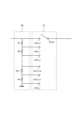
- FIG. 1 is a circuit diagram showing a circuit configuration of a push switch and a resistive voltage divider circuit included in an optical element driving circuit section of an illumination device according to an embodiment of the present invention.
- FIG. 4 is a schematic diagram showing a signal input to an optical element of an illumination device according to one embodiment of the present invention.
- FIG. 2 is a block diagram showing a circuit configuration of an optical element driving circuit section of an illumination device according to an embodiment of the present invention.
- FIG. 2 is a block diagram showing a circuit configuration of an optical element driving circuit section of an illumination device according to an embodiment of the present invention.
- FIG. 1 is a schematic block diagram showing an internal configuration of a lighting device according to an embodiment of the present invention; 4 is a schematic diagram showing a signal input to an optical element of an illumination device according to one embodiment of the present invention.
- drawings may show the width, thickness, shape, etc. of each part in a schematic manner compared to the actual embodiment, but these are merely examples, and the illustrated shapes themselves do not limit the interpretation of the present invention.
- components with the same functions as those explained in relation to previous drawings in the specification may be given the same reference numerals even in separate drawings, and duplicate explanations may be omitted.
- each structure When a film is processed to form multiple structures, each structure may have a different function or role, and each structure may be formed on a different base.
- these multiple structures originate from a film formed as the same layer in the same process, and are made of the same material. Therefore, these multiple films are defined as existing in the same layer.
- FIG. 1A First Embodiment An illumination device 1 according to an embodiment of the present invention will be described with reference to FIGS. 1A to 7.
- FIG. 1A First Embodiment An illumination device 1 according to an embodiment of the present invention will be described with reference to FIGS. 1A to 7.
- FIG. 1A First Embodiment An illumination device 1 according to an embodiment of the present invention will be described with reference to FIGS. 1A to 7.
- Configuration of lighting device 1] 1A and 1B are schematic side and top views, respectively, illustrating the configuration of an illumination device 1 according to one embodiment of the present invention.
- the lighting device 1 includes a main body 1a and a lighting unit 1b.
- the lighting unit 1b is connected to an end of the main body 1a.
- the main body 1a has a cylindrical shape, and light is emitted from the lighting unit 1b. While holding the main body 1a, the user can illuminate the surroundings of the user with the light emitted from the lighting unit 1b. In this way, the lighting device 1 can be used as a flashlight. However, the usage of the lighting device 1 is not limited to this.
- the lighting device 1 can also be used as a spotlight.
- the direction in which the main body 1a extends is defined as the z-axis direction when viewed from above.
- the emission direction of the light emitted from the illumination unit 1b is the z-axis direction.
- the direction perpendicular to the z-axis direction is defined as the x-axis direction.
- the diffusion direction of the light emitted from the illumination unit 1b is the x-axis direction.
- the direction perpendicular to the z-axis and x-axis directions is defined as the y-axis direction.
- the main body 1a has a curved shape. Specifically, the main body 1a extends parallel to the z-axis direction and has a shape in which a portion parallel to the z-axis direction that is connected to the lighting unit 1b is combined with a portion extending in a direction not parallel to the z-axis direction.
- the main body 1a has such a shape, even when the user uses the lighting device 1 close to the user's face, the user can hold the main body 1a without applying excessive force to the user's wrist to illuminate the user's surroundings.
- the shape of the main body 1a is not limited to this.
- the shape of the main body 1a can be a shape that corresponds to the usage manner of the lighting device 1.
- the upper surface of the main body 1a is provided with a push button for a push switch 61.
- the push switch 61 adjusts the light distribution angle of the light emitted from the lighting unit 1b. That is, when the user presses the push button for the push switch 61, the light distribution angle of the light emitted from the lighting unit 1b changes in stages.
- the main body 1a also includes a light source adjustment switch 71 that adjusts the brightness of the light emitted from the lighting unit 1b.
- a knob for a slide switch or a push button for a push switch may be provided on the side of the main body 1a.
- the light source adjustment switch 71 is a slide switch, the brightness of the light emitted from the lighting unit 1b can be continuously adjusted by sliding the knob.
- the light source adjustment switch 71 is a push switch, the brightness of the light emitted from the lighting unit 1b can be adjusted in stages by pressing the push button for the push switch.
- FIG. 1C is a schematic block diagram showing the internal configuration of a lighting device 1 according to one embodiment of the present invention.
- the lighting device 1 includes an optical element 10, a light source 20, an optical adjustment unit 30, a battery 40, a charging module 50, an optical element drive circuit unit 60, and a light source drive circuit unit 70.
- the optical element 10, the light source 20, and the optical adjustment unit 30 are housed in the lighting unit 1b.
- the battery 40, the charging module 50, the optical element drive circuit unit 60, and the light source drive circuit unit 70 are housed in the main body unit 1a.
- FIG. 1C shows the connections between the components.
- the optical element drive circuit unit 60 is connected to the optical element 10 and the battery 40.
- the optical element drive circuit unit 60 receives power from the battery 40, and generates a signal to drive the optical element 10.
- the optical element drive circuit unit 60 is also connected to a push switch 61.
- the light source drive circuit unit 70 is connected to the light source 20 and the battery 40.
- the light source drive circuit unit 70 receives power from the battery 40, and generates a signal to drive the light source 20.
- the light source drive circuit unit 70 is also connected to a light source adjustment switch 71.
- the battery 40 is connected to the charging module 50.
- the battery 40 can be a so-called secondary battery (e.g., lithium ion battery, etc.) that can be used repeatedly by charging.
- the battery 40 can be charged via the charging module 50.
- the charging module 50 controls the charging of the battery 40 while preventing overcharging of the battery 40.
- the battery 40 can be charged in a wired or wireless configuration. In a wired configuration, the charging module 50 is provided with a terminal for connecting a power cable, and power is charged to the battery 40 via the power cable connected to the terminal of the charging module 50. In a wireless configuration, a power receiving coil is provided in the charging module 50, and the power converted by the power receiving coil is charged to the battery 40.
- a configuration in which the charging module 50 is not provided can also be applied to the lighting device 1.
- a so-called primary battery e.g., alkaline dry battery or manganese dry battery, etc.
- the battery 40 can be used as the battery 40.
- the light source 20 emits light to the optical element 10.
- a light emitting diode LED
- a plurality of LEDs may be used as the light source 20.
- LEDs of the same color may be used, or LEDs of different colors may be used.
- the light source 20 is not limited to an LED.
- the light source 20 may be any element or device that can emit light.
- the optical adjustment unit 30 is disposed between the optical element 10 and the light source 20, and converges, diffuses, or reflects the light emitted from the light source 20.
- the optical adjustment unit 30 is an optical component that is a lens or a reflector, or a combination of these.
- FIG. 2A and 2B are schematic cross-sectional views showing a configuration of an optical element 10 of an illumination device 1 according to an embodiment of the present invention.
- Fig. 2A is a cross-sectional view of the optical element 10 cut along a plane perpendicular to the y-axis direction
- Fig. 2B is a cross-sectional view of the optical element 10 cut along a plane perpendicular to the x-axis direction.
- the optical element 10 includes four liquid crystal cells 100 (first liquid crystal cell 100-1, second liquid crystal cell 100-2, third liquid crystal cell 100-3, and fourth liquid crystal cell 100-4).
- the first liquid crystal cell 100-1, second liquid crystal cell 100-2, third liquid crystal cell 100-3, and fourth liquid crystal cell 100-4 are stacked in order in the z-axis direction from the side closest to the light source 20.
- Light emitted from the light source 20 is incident on the first liquid crystal cell 100-1 and is emitted from the fourth liquid crystal cell 100-4.
- the diffusion and polarization of light are controlled by the four liquid crystal cells 100 included in the optical element 10, and the light distribution of the light emitted from the fourth liquid crystal cell 100-4 can be changed. That is, the optical element 10 transmits the light emitted from the light source 20 in a diffusible manner and can control the light distribution.
- FIGS 2A and 2B show the configuration of an optical element 10 including four liquid crystal cells 100, but the number of liquid crystal cells 100 included in the optical element 10 is not limited to four. It is sufficient that the optical element 10 includes at least one liquid crystal cell 100.
- each of the first liquid crystal cell 100-1 to the fourth liquid crystal cell 100-4 includes a first substrate 110-1, a second substrate 110-2, a plurality of first transparent electrodes 120-1, a plurality of second transparent electrodes 120-2, a plurality of third transparent electrodes 120-3, a plurality of fourth transparent electrodes 120-4, a first alignment film 130-1, a second alignment film 130-2, a sealant 140, and a liquid crystal layer 150.
- the first transparent electrodes 120-1 and the second transparent electrodes 120-2 are alternately provided on the first substrate 110-1.
- a first alignment film 130-1 is provided on the first substrate 110-1 so as to cover the first transparent electrodes 120-1 and the second transparent electrodes 120-2.
- a third transparent electrode 120-3 and a fourth transparent electrode 120-4 are alternately provided on the second substrate 110-2.
- a second alignment film 130-2 is provided so as to cover the third transparent electrode 120-3 and the fourth transparent electrode 120-4.
- the first substrate 110-1 and the second substrate 110-2 are disposed so that the first transparent electrode 120-1 and the second transparent electrode 120-2 face the third transparent electrode 120-3 and the fourth transparent electrode 120-4, and are bonded via a sealant 140 provided on the periphery of the first substrate 110-1 and the second substrate 110-2.
- a liquid crystal is sealed in the space surrounded by the first substrate 110-1 (more specifically, the first alignment film 130-1), the second substrate 110-2 (more specifically, the second alignment film 130-2), and the sealant 140, and a liquid crystal layer 150 is provided between the first substrate 110-1 and the second substrate 110-2.
- An optically elastic resin layer 160 is provided between the first liquid crystal cell 100-1 and the second liquid crystal cell 100-2. Similarly, an optically elastic resin layer 160 is provided between the second liquid crystal cell 100-2 and the third liquid crystal cell 100-3, and between the third liquid crystal cell 100-3 and the fourth liquid crystal cell 100-4.
- an adhesive containing a light-transmitting acrylic resin can be used as the optically elastic resin layer 160. In other words, the optically elastic resin layer 160 can bond and fix two adjacent liquid crystal cells 100 together.
- Each of the first substrate 110-1 and the second substrate 110-2 may be a rigid substrate having optical transparency, such as a glass substrate, a quartz substrate, or a sapphire substrate. Also, each of the first substrate 110-1 and the second substrate 110-2 may be a flexible substrate having optical transparency, such as a polyimide resin substrate, an acrylic resin substrate, a siloxane resin substrate, or a fluororesin substrate.
- Each of the first transparent electrode 120-1, the second transparent electrode 120-2, the third transparent electrode 120-3, and the fourth transparent electrode 120-4 functions as an electrode for forming an electric field in the liquid crystal layer 150.
- Each of the first transparent electrode 120-1, the second transparent electrode 120-2, the third transparent electrode 120-3, and the fourth transparent electrode 120-4 is made of a transparent conductive material such as indium tin oxide (ITO) or indium zinc oxide (IZO).
- the first transparent electrode 120-1 and the second transparent electrode 120-2 extend in the x-axis direction
- the third transparent electrode 120-3 and the fourth transparent electrode 120-4 extend in the y-axis direction
- the first transparent electrode 120-1 and the second transparent electrode 120-2 extend in the y-axis direction
- the third transparent electrode 120-3 and the fourth transparent electrode 120-4 extend in the x-axis direction.
- transparent electrodes 120 when there is no particular distinction between the first transparent electrode 120-1 to the fourth transparent electrode 120-4, they may be referred to as transparent electrodes 120.
- the first alignment film 130-1 and the second alignment film 130-2 each align the liquid crystal molecules in the liquid crystal layer 150 in a predetermined direction.
- a polyimide resin or the like is used as each of the first alignment film 130-1 and the second alignment film 130-2.
- each of the first alignment film 130-1 and the second alignment film 130-2 may be given alignment characteristics by an alignment treatment such as a rubbing method or a photo-alignment method.
- the rubbing method is a method in which the surface of the alignment film is rubbed in one direction.
- the photo-alignment method is a method in which the alignment film is irradiated with linearly polarized ultraviolet light.
- the first alignment film 130-1 is oriented so that the liquid crystal molecules on the first substrate 110-1 side of the liquid crystal layer 150 are aligned in a direction perpendicular to the extension direction of the first transparent electrode 120-1 and the second transparent electrode 120-2.
- the second alignment film 130-2 is oriented so that the liquid crystal molecules on the second substrate 110-2 side of the liquid crystal layer 150 are aligned in a direction perpendicular to the extension direction of the third transparent electrode 120-3 and the fourth transparent electrode 120-4.
- the long axes of the liquid crystal molecules on the first substrate 110-1 side are oriented in the y-axis direction, and the long axes of the liquid crystal molecules on the second substrate 110-2 side are oriented in the x-axis direction.
- the long axes of the liquid crystal molecules on the first substrate 110-1 side are aligned in the x-axis direction, and the long axes of the liquid crystal molecules on the second substrate 110-2 side are aligned in the y-axis direction.
- an adhesive containing epoxy resin or acrylic resin is used as the sealing material 140.
- the adhesive may be of the ultraviolet curing type or the heat curing type.
- the liquid crystal layer 150 can refract the light passing through it or change the polarization state of the light passing through it depending on the orientation state of the liquid crystal molecules.
- Nematic liquid crystals or the like are used as the liquid crystal for the liquid crystal layer 150.
- the liquid crystal described in this embodiment is of the positive type, but it is also possible to apply a negative type by changing the orientation direction of the liquid crystal molecules when no voltage is applied to the transparent electrode 120.
- the liquid crystal contains a chiral agent that imparts a twist to the liquid crystal molecules.
- Electrode pattern of liquid crystal cell 100 3A and 3B are schematic plan views showing the electrode patterns of the liquid crystal cell 100 included in the optical element 10 of the illumination device 1 according to one embodiment of the present invention. Specifically, Fig. 3A is a plan view showing the electrode patterns formed on the first substrate 110-1 of the first liquid crystal cell 100-1, and Fig. 3B is a plan view showing the electrode patterns formed on the second substrate 110-2 of the first liquid crystal cell 100-1.
- a first connection pad 121-1 and a second connection pad 121-2 are provided on the first substrate 110-1.
- the first transparent electrodes 120-1 are electrically connected to the first connection pad 121-1.
- the second transparent electrodes 120-2 are electrically connected to the second connection pad 121-2.
- a first alignment film 130-1 is provided on the first transparent electrodes 120-1 and the second transparent electrodes 120-2 (not shown in FIG. 3A).
- the first alignment film 130-1 has been subjected to an alignment treatment, and the alignment direction of the first alignment film 130-1 is the y-axis direction.
- the second substrate 110-2 is provided with a third connection pad 121-3, a fourth connection pad 121-4, a first terminal 122-1, a second terminal 122-2, a third terminal 122-3, and a fourth terminal 122-4.
- the third transparent electrodes 120-3 are electrically connected to the third terminal 122-3.
- the fourth transparent electrodes 120-4 are electrically connected to the fourth terminal 122-4.
- the third connection pad 121-3 is electrically connected to the first terminal 122-1.
- the fourth connection pad 121-4 is electrically connected to the second terminal 122-2.
- a second alignment film 130-2 is provided on the third transparent electrodes 120-3 and the fourth transparent electrodes 120-4 (not shown in FIG. 3B).
- the second alignment film 130-2 has been subjected to alignment treatment, and the alignment direction of the first alignment film 130-1 is the x-axis direction.
- the first connection pad 121-1 and the second connection pad 121-2 overlap with the third connection pad 121-3 and the fourth connection pad 121-4, respectively.
- a conductive electrode is provided between the first connection pad 121-1 and the third connection pad 121-3, and the first connection pad 121-1 and the third connection pad 121-3 are electrically connected via the conductive electrode.
- a conductive electrode is provided between the second connection pad 121-2 and the fourth connection pad 121-4, and the second connection pad 121-2 and the fourth connection pad 121-4 are electrically connected via the conductive electrode. Therefore, the first transparent electrode 120-1 and the second transparent electrode 120-2 on the first substrate 110-1 are electrically connected to the first terminal 122-1 and the second terminal 122-2, respectively.
- the electrode pattern of the second liquid crystal cell 100-2 is the same as the electrode pattern of the first liquid crystal cell 100-1.
- the configuration of the electrode patterns of the third liquid crystal cell 100-3 and the fourth liquid crystal cell 100-4 is similar to the configuration of the electrode pattern of the first liquid crystal cell 100-1, except that the extension direction of the transparent electrode 120 differs by 90°.
- the first terminal 122-1 to the fourth terminal 122-4 on the second substrate 110-2 are exposed from the first substrate 110-1.
- the exposed first terminal 122-1 to the fourth terminal 122-4 are electrically connected to the optical element driving circuit unit 60.
- a signal generated in the optical element driving circuit unit 60 is input to the first terminal 122-1 to the fourth terminal 122-4 of each of the first liquid crystal cell 100-1 to the fourth liquid crystal cell 100-4, and a predetermined potential is applied to each of the first transparent electrode 120-1 to the fourth transparent electrode 120-4 of each of the first liquid crystal cell 100-1 to the fourth liquid crystal cell 100-4. This changes the alignment state of the liquid crystal molecules in the liquid crystal layer 150 of each of the first liquid crystal cell 100-1 to the fourth liquid crystal cell 100-4, and can change the distribution of light passing through the optical element 10.
- FIG. 4A and 4B are schematic diagrams illustrating optical characteristics of the liquid crystal cell 100 included in the optical element 10 of the lighting device 1 according to one embodiment of the present invention. Specifically, Fig. 4A shows the liquid crystal cell 100 in a state where no voltage is applied to the transparent electrode 120, and Fig. 4B shows the liquid crystal cell 100 in a state where a voltage is applied to the transparent electrode 120.
- the liquid crystal molecules on the first substrate 110-1 side of the liquid crystal layer 150 are aligned in the y-axis direction, and the liquid crystal molecules on the second substrate 110-2 side of the liquid crystal layer 150 are aligned in the x-axis direction. Therefore, when no voltage is applied to any of the first transparent electrode 120-1 to the fourth transparent electrode 120-4, the liquid crystal molecules in the liquid crystal layer 150 are aligned so as to be twisted 90° as they move from the first substrate 110-1 to the second substrate 110-2. Furthermore, the polarization plane (the direction of the polarization axis or polarization component) of the light passing through the liquid crystal layer 150 is rotated 90° according to the orientation direction of the liquid crystal molecules. In other words, the light passing through the liquid crystal layer 150 (more specifically, the polarization component of the light passing through the liquid crystal layer 150) is rotated.
- the liquid crystal molecules in the liquid crystal layer 150 are oriented so as to be twisted 90° from the first substrate 110-1 toward the second substrate 110-2, while the liquid crystal molecules near the first substrate 110-1 are arranged in a convex arc shape relative to the first substrate 110-1 due to the transverse electric field between the first transparent electrode 120-1 and the second transparent electrode 120-2, and the liquid crystal molecules near the second substrate 110-2 are arranged in a convex arc shape relative to the second substrate 110-2 due to the transverse electric field between the third transparent electrode 120-3 and the fourth transparent electrode 120-4.
- the liquid crystal molecules arranged in a convex arc shape have a refractive index distribution, and the polarized component of light along the orientation direction of the liquid crystal molecules is diffused.
- the cell gap d which is the distance between the first substrate 110-1 and the second substrate 110-2, is sufficiently larger than the distance between the two adjacent transparent electrodes 120 (for example, 8 ⁇ m ⁇ d ⁇ 50 ⁇ m, preferably 10 ⁇ m ⁇ d ⁇ 30 ⁇ m, and more preferably 15 ⁇ m ⁇ d ⁇ 25 ⁇ m), so the electric field formed between the transparent electrodes 120 does not have much effect on the liquid crystal molecules located near the center between the first substrate 110-1 and the second substrate 110-2.
- the light emitted from the light source 20 contains a polarized component in the x-axis direction (hereinafter referred to as the "P polarized component”) and a polarized component in the y-axis direction (hereinafter referred to as the "S polarized component").
- P polarized component a polarized component in the x-axis direction
- S polarized component a polarized component in the y-axis direction
- the light entering the liquid crystal cell 100 will be described below as being divided into a first light 1000-1 having a P polarized component and a second light 1000-2 having an S polarized component.
- the P-polarized component of the first light 1000-1 incident on the liquid crystal layer 150 from the first substrate 110-1 is different from the orientation direction of the liquid crystal molecules on the first substrate 110-1 side, so the first light 1000-1 is not diffused (see (1) in FIG. 4B).
- the first light 1000-1 is rotated while passing through the liquid crystal layer 150, and the polarization component changes from the P-polarized component to the S-polarized component.
- the S-polarized component of the first light 1000-1 is different from the orientation direction of the liquid crystal molecules on the second substrate 110-2 side, so the first light 1000-1 is not diffused (see (2) in FIG. 4B).
- the S-polarized component of the second light 1000-2 incident on the liquid crystal layer 150 from the first substrate 110-1 is aligned in the same direction as the liquid crystal molecules on the first substrate 110-1 side, so the second light 1000-2 is diffused in the y-axis direction according to the refractive index distribution of the liquid crystal molecules (see (3) in FIG. 4B).
- the second light 1000-2 is rotated while passing through the liquid crystal layer 150, and the polarization component changes from the S-polarized component to the P-polarized component.
- the P-polarized component of the second light 1000-2 is aligned in the same direction as the liquid crystal molecules on the second substrate 110-2 side, so the second light 1000-2 is diffused in the x-axis direction according to the refractive index distribution of the liquid crystal molecules (see (4) in FIG. 4B).
- FIG. 5 is a block diagram showing a circuit configuration of the optical element driving circuit section 60 of the lighting device 1 according to an embodiment of the present invention. Note that Fig. 5 shows an example of the circuit configuration of the optical element driving circuit section 60, and the circuit configuration of the optical element driving circuit section 60 is not limited thereto. Also, components that can be understood by those skilled in the art may be omitted in Fig. 5.
- the optical element driving circuit section 60 includes a push switch 61, a resistive voltage dividing circuit 66, a first transistor Tr1, a second transistor Tr2, a third transistor Tr3, and an oscillator OSC.
- a potential is supplied to the optical element driving circuit section 60 from a battery 40.
- the potential output from the battery 40 is, for example, 15 V, but is not limited to this. However, for the sake of convenience, the following description will be given assuming that the output potential of the battery 40 is 15 V.
- the resistive voltage divider circuit 66 is electrically connected to the battery 40.
- the resistive voltage divider circuit 66 is also electrically connected to the push switch 61.
- the resistive voltage divider circuit 66 divides the 15V potential supplied from the battery 40 in stages to generate multiple potentials.
- the push switch 61 selects and outputs one of the multiple potentials generated by the resistive voltage divider circuit 66.
- the circuit configuration of the push switch 61 and the resistive voltage divider circuit 66 will be described with reference to FIG. 6.
- FIG. 6 is a circuit diagram showing the circuit configuration of a push switch 61 and a resistive voltage divider circuit 66 included in an optical element driving circuit section 60 of an illumination device 1 according to one embodiment of the present invention.
- the resistive voltage divider circuit 66 includes a number of resistors R1, R2, ..., Rn-1, Rn (n is a natural number).
- the push switch 61 also includes a number of input side contacts 61in_0, 61in_1, 61in_2, ..., 61in_n-2, 61in_n-1, 61in_n, and an output side contact 61out.
- a potential of 15V is divided according to the number of resistors R1, R2, ..., Rn-1, Rn, and a number of potentials in the range of 0 to 15V are generated.
- the generated potentials are input to each of the input side contacts 61in_0, 61in_1, 61in_2, ..., 61in_n-2, 61in_n-1, 61in_n.
- the input contact 61in_0 is electrically connected to the battery 40 without passing through the resistors R1, R2, ..., Rn-1, Rn, and 15 V is input to the input contact 61in_0.
- the input contact 61in_n is electrically connected to GND (0 V), and 0 V is input to the input contact 61in_n.
- a potential according to the division ratio of the resistors R1, R2, ..., Rn-1, Rn is input to each of the input contacts 61in_1, 61in_2, ..., 61in_n-2, 61in_n-1. That is, potentials of different magnitudes are input to each of the input contacts 61in_0, 61in_1, 61in_2, ..., 61in_n-2, 61in_n-1, 61in_n.
- the potential generated by the resistive voltage divider circuit 66 is a stepped (discontinuous) potential within the range of 0 to 15 V.
- the potentials input to the multiple input side contacts 61in_0, 61in_1, 61in_2, ..., 61in_n-2, 61in_n-1, 61in_n decrease from 15 V to 0 V in that order, but the interval between the potentials input to two adjacent input side contacts may be the same or different.
- one of the multiple input side contacts 61in_0, 61in_1, 61in_2, ..., 61in_n-2, 61in_n-1, 61in_n is selected, and one of the multiple input side contacts 61in_0, 61in_1, 61in_2, ..., 61in_n-2, 61in_n-1, 61in_n is electrically connected to the output side contact 61out.
- the electrical connection with the output side contact 61out may be switched in the order of input side contacts 61in_0, 61in_1, 61in_2, ..., 61in_n-2, 61in_n-1, 61in_n, or the electrical connection with the output side contact 61out may be switched in the order of input side contacts 61in_n, 61in_n-1, 61in_n-2, ..., 61in_2, 61in_1, 61in_0.
- the electrical connection with the output side contact 61out may be switched in the order of the input side contacts 61in_0, 61in_1, 61in_2, ..., 61in_n-2, 61in_n-1, 61in_n, and then the electrical connection with the output side contact 61out may be switched again in the order of the input side contacts 61in_0, 61in_1, 61in_2, ..., 61in_n-2, 61in_n-1, 61in_n, or the electrical connection with the output side contact 61out may be switched in the order of the input side contacts 61in_n-1, 61in_n-2, ..., 61in_2, 61in_1, 61in_0, and then the electrical connection with the output side contact 61out may be switched again in the order of the input side contacts 61in_n-1, 61in_n-2, ..., 61in_2, 61in_1, 61in_0.
- the resistive voltage divider circuit 66 and the push switch 61 can generate multiple potentials in stages from the input potential, and select and output one of the multiple generated potentials.
- the potential to be output can be controlled by operating the push button of the push switch 61.
- optical element driving circuit unit 60 will be described.
- the optical element driving circuit section 60 includes a first output terminal 67_1, a second output terminal 67_2, a third output terminal 67_3, a fourth output terminal 67_4, and a fifth output terminal 67_5.
- a signal for driving the optical element 10 is generated, and a first signal S1, a second signal S2, a third signal S3, a fourth signal S4, and a fifth signal S5 are output from the first output terminal 67_1, the second output terminal 67_2, the third output terminal 67_3, the fourth output terminal 67_4, and the fifth output terminal 67_5, respectively.
- the oscillator OSC is electrically connected to the gate of the first transistor Tr1 and the gate of the second transistor Tr2.
- the oscillator OSC generates and outputs a square wave.
- the frequency of the square wave is, for example, 60 Hz, but is not limited to this.
- the square wave output from the oscillator OSC is input to the gate of the first transistor Tr1 and the gate of the second transistor Tr2. Therefore, each of the first transistor Tr1 and the second transistor Tr2 repeats an on state and an off state according to the frequency of the square wave.
- One of the source and drain of the first transistor Tr1 is electrically connected to the output contact of the push switch 61 via the contact C1.
- the contact C1 is electrically connected to the first output terminal 67_1 via the node N1.
- the other of the source and drain of the first transistor Tr1 is electrically connected to GND (0V). Therefore, when the first transistor Tr1 is in the on state, the potential of the node N1 is 0V. On the other hand, when the first transistor Tr1 is in the off state, the potential of the node N1 is a predetermined potential selected by operating the push button of the push switch 61.
- the first signal S1 having the first pulse wave PW1 with the predetermined potential as an amplitude is output from the first output terminal 67_1 electrically connected to the node N1.
- the first pulse wave PW1 has a phase that is the inverted phase of the rectangular wave generated by the oscillator OSC.
- One of the source and drain of the second transistor Tr2 is electrically connected to the battery 40 via contact C2.
- Contact C2 is electrically connected to the gate of the third transistor Tr3 via node N2.
- the other of the source and drain of the second transistor Tr2 is electrically connected to GND (0V). Therefore, when the second transistor Tr2 is in the on state, the potential of the node N2 is 0V. On the other hand, when the second transistor Tr2 is in the off state, the potential of the node N2 is 15V. In other words, the potential of the node N2 alternates between 0V and 15V depending on the frequency of the square wave.
- the gate of the third transistor Tr3 is electrically connected to the node N2.
- One of the source and drain of the third transistor Tr3 is electrically connected to the output contact of the push switch 61 through the contact C3.
- the contact C3 is electrically connected to the second output terminal 67_2 through the node N3.
- the other of the source and drain of the third transistor Tr3 is electrically connected to GND (0V). Therefore, when the third transistor Tr3 is in the on state, the potential of the node N3 is 0V. On the other hand, when the third transistor Tr3 is in the off state, the potential of the node N3 is a predetermined potential selected by operating the push button of the push switch 61.
- the second signal S2 having the second pulse wave PW2 with the predetermined potential as an amplitude is output from the second output terminal 67_2 electrically connected to the node N3.
- the second pulse wave PW2 has the same phase as the phase of the rectangular wave generated by the oscillator OSC.
- the third output terminal 67_3 to the fifth output terminal 67_5 are electrically connected to the output contact 61out of the push switch 61. Therefore, the third signal S3 to the fifth signal S5 output from the third output terminal 67_3 to the fifth output terminal 67_5 have a fixed potential P fix corresponding to a predetermined potential.
- a resistive voltage divider circuit may be electrically connected to the fifth output terminal 67_5, and the fifth signal S5 having a fixed potential (for example, an intermediate potential of a predetermined potential) generated by the resistive voltage divider circuit may be output from the fifth output terminal 67_5.
- the first signal S1 to the fourth signal S4 generated by the optical element driving circuit unit 60 are input to the optical element 10.
- the signals input to the optical element 10 and the driving of the optical element 10 in the lighting device 1 will be described.
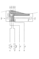
- FIG. 7 is a schematic diagram showing a signal input to the optical element 10 of the lighting device 1 according to one embodiment of the present invention.
- the first liquid crystal cell 100-1 of the optical element 10 is shown.
- the first signal S1 to the fourth signal S4 are input to the first terminal 122-1 to the fourth terminal 122-4, respectively.
- the first terminal 122-1 to the fourth terminal 122-4 are electrically connected to the first transparent electrode 120-1 to the fourth transparent electrode 120-4, respectively. Therefore, a first pulse wave PW1 is applied to the first transparent electrode 120-1, a second pulse wave PW2 is applied to the second transparent electrode 120-2, and a fixed potential P fix is applied to the third transparent electrode 120-3 and the fourth transparent electrode 120-4.
- the first pulse wave PW1 and the second pulse wave PW2 have the same amplitude, but the phases are inverted. Therefore, a transverse electric field is generated between the first transparent electrode 120-1 and the second transparent electrode 120-2, and the alignment state of the liquid crystal molecules on the first substrate 110-1 side changes. Since the same fixed potential P fix is applied to the third signal S3 and the fourth signal S4, no transverse electric field is generated between the third transparent electrode 120-3 and the fourth transparent electrode 120-4, and the alignment state of the liquid crystal molecules on the second substrate 110-2 side does not change. In this case, the light passing through the first liquid crystal cell 100-1 is diffused in the y-axis direction.
- the diffusion angle in the y-axis direction changes depending on the magnitude of the amplitude of the first pulse wave PW1 and the second pulse wave PW2, but the diffusion angle in the y-axis direction can be easily adjusted by operating the push button of the push switch 61.
- the light emitted from the lighting device 1 has a linear light distribution shape that is extended in the y-axis direction.
- the lighting device 1 can emit light having a linear light distribution shape stretched in one axis direction (y-axis direction).
- the light distribution angle of the light emitted from the lighting device 1 is controlled in stages by operating the push button of the push switch 61. That is, the user can change the output from the output side contact 61out in stages by pressing the push button of the push switch 61.
- This allows the amplitude of the first pulse wave PW1 and the second pulse wave PW2 to be changed in stages. Since the amplitude of each pulse wave corresponds to the potential difference between the transparent electrodes 120 of each liquid crystal cell 100 of the optical element 10, the potential difference between the transparent electrodes increases as the amplitude of the pulse wave increases.
- the refractive index distribution of the liquid crystal molecules increases, and the light distribution angle increases.
- the potential difference between the transparent electrodes decreases as the amplitude of the pulse wave decreases.
- the refractive index distribution of the liquid crystal molecules decreases, and the light distribution angle also decreases. In this way, the light distribution angle of the light emitted from the lighting device 1 can be easily adjusted by simply pressing the push switch 61. By pressing the push switch 61, the magnitude of the fixed potential Pfix can also be changed.
- the lighting device 1 can be modified in various ways. Below, several modified examples of the optical element drive circuit section 60 of the lighting device 1 are described. Note that below, descriptions of configurations similar to the configuration of the optical element drive circuit section 60 may be omitted.
- FIG. 8 is a block diagram showing the circuit configuration of the optical element driving circuit section 60A of the lighting device 1 according to one embodiment of the present invention.
- the first output terminal 67_1 and the third output terminal 67_3 are electrically connected to the node N1. Therefore, the first signal S1 output from the first output terminal 67_1 and the third signal S3 output from the third output terminal 67_3 each have a first pulse wave PW1.
- the second output terminal 67_2 and the fourth output terminal 67_4 are electrically connected to the node N3. Therefore, the second signal S2 output from the second output terminal 67_2 and the fourth signal S4 output from the fourth output terminal 67_4 each have a second pulse wave PW2.
- the fifth output terminal 67_5 is electrically connected to the output side contact 61out of the push switch 61. Therefore, the fifth signal S5 output from the fifth output terminal 67_5 has a fixed potential P fix corresponding to a predetermined potential.
- the first signal S1 to the fourth signal S4 are input to the first terminal 122-1 to the fourth terminal 122-4, respectively.
- the first terminal 122-1 to the fourth terminal 122-4 are electrically connected to the first transparent electrode 120-1 to the fourth transparent electrode 120-4, respectively. Therefore, the first pulse wave PW1 is applied to the first transparent electrode 120-1 and the third transparent electrode 120-3, and the second pulse wave PW2 is applied to the second transparent electrode 120-2 and the fourth transparent electrode 120-4.
- the first pulse wave PW1 and the second pulse wave PW2 have the same amplitude but inverted phase. Therefore, a transverse electric field is generated between the first transparent electrode 120-1 and the second transparent electrode 120-2, changing the alignment state of the liquid crystal molecules on the first substrate 110-1 side. Also, a transverse electric field is generated between the third transparent electrode 120-3 and the fourth transparent electrode 120-4, changing the alignment state of the liquid crystal molecules on the second substrate 110-2 side.
- the light passing through the first liquid crystal cell 100-1 is diffused in the x-axis and y-axis directions. Therefore, the light irradiated from the lighting device 1 according to this modified example has a circular light distribution shape diffused in the x-axis and y-axis directions.
- the lighting device 1 can emit light having a circular light distribution shape.
- the light distribution angle of the light emitted from the lighting device 1 is controlled in stages by operating the push button of the push switch 61. In other words, the user can easily adjust the light distribution angle of the light emitted from the lighting device 1 by simply pressing the push button of the push switch 61.
- FIG. 9 is a block diagram showing the circuit configuration of the optical element driving circuit section 60B of the lighting device 1 according to one embodiment of the present invention.
- the optical element driving circuit section 60B includes a first output terminal 67_1, a second output terminal 67_2, a third output terminal 67_3, a fourth output terminal 67_4, a fifth output terminal 67_5, and a sixth output terminal 67_6.
- a signal for driving the optical element 10 is generated, and a first signal S1, a second signal S2, a third signal S3, a fourth signal S4, a fifth signal S5, and a sixth signal S6 are output from the first output terminal 67_1, the second output terminal 67_2, the third output terminal 67_3, the fourth output terminal 67_4, the fifth output terminal 67_5, and the sixth output terminal 67_6, respectively.
- the optical element driving circuit section 60B includes two push switches 61 and two resistive voltage divider circuits 66.
- the resistive voltage divider circuit 66 and the push switch 61 are used not only to generate the first signal S1 and the second signal S2, but also to generate the third signal S3 and the fourth signal S4.
- a circuit connected to one of the two push switches 61 includes a first output terminal 67_1, a second output terminal 67_2, and a fifth output terminal 67_5, and the first signal S1, the second signal S2, and the fifth signal S5 are output from the first output terminal 67_1, the second output terminal 67_2, and the fifth output terminal 67_5, respectively.
- the circuit connected to the other of the two push switches 61 includes a third output terminal 67_3, a fourth output terminal 67_4, and a sixth output terminal 67_6, and a third signal S3, a fourth signal S4, and a sixth signal S6 are output from the third output terminal 67_3, the fourth output terminal 67_4, and the sixth output terminal 67_6, respectively.
- the first signal S1 and the third signal S3 each have a first pulse wave PW1
- the second signal S2 and the fourth signal S4 each have a second pulse wave PW2
- the fifth signal S5 and the sixth signal S6 each have a fixed potential P fix corresponding to a predetermined potential.
- the first signal S1 to the fourth signal S4 are input to the first terminal 122-1 to the fourth terminal 122-4, respectively.
- the first terminal 122-1 to the fourth terminal 122-4 are electrically connected to the first transparent electrode 120-1 to the fourth transparent electrode 120-4, respectively. Therefore, the first pulse wave PW1 is applied to the first transparent electrode 120-1 and the third transparent electrode 120-3, and the second pulse wave PW2 is applied to the second transparent electrode 120-2 and the fourth transparent electrode 120-4.
- the first pulse wave PW1 and the second pulse wave PW2 have the same amplitude but inverted phase. Therefore, a transverse electric field is generated between the first transparent electrode 120-1 and the second transparent electrode 120-2, changing the alignment state of the liquid crystal molecules on the first substrate 110-1 side. Also, a transverse electric field is generated between the third transparent electrode 120-3 and the fourth transparent electrode 120-4, changing the alignment state of the liquid crystal molecules on the second substrate 110-2 side.
- the light passing through the first liquid crystal cell 100-1 is diffused in the x-axis and y-axis directions. Therefore, the light irradiated from the lighting device 1 according to this modified example has a circular light distribution shape diffused in the x-axis and y-axis directions.
- the lighting device 1 can emit light having a circular light distribution shape.
- the light distribution angle of the light emitted from the lighting device 1 is controlled in stages by operating the push button of the push switch 61. That is, the user can easily adjust the light distribution angle of the light emitted from the lighting device 1 by simply pressing the push button of the push switch 61.
- the amplitudes of the first pulse wave PW1 and the second pulse wave PW2 of the first signal S1 and the second signal S2 and the amplitudes of the first pulse wave PW1 and the second pulse wave PW2 of the third signal S3 and the fourth signal are controlled by each push switch 61.
- the light distribution angle in the x-axis direction and the light distribution angle in the y-axis direction can be adjusted separately and independently, and not only a circular shape but also an elliptical shape can be formed.
- FIG. 10 is a schematic block diagram showing the internal configuration of a lighting device 2 according to one embodiment of the present invention.
- the lighting device 2 includes an optical element 10, a light source 20, an optical adjustment unit 30, a battery 40, a charging module 50, an optical element driving circuit unit 60, and a light source driving circuit unit 70.
- the optical element driving circuit unit 60 of the lighting device 2 is connected to not only a push switch 61 but also a push switch 62.
- the push switch 62 is disposed between the optical element driving circuit unit 60 and the optical element 10.
- the optical element 10 is electrically connected to the optical element driving circuit unit 60 via the push switch 62.
- the push button of the push switch 62 is provided on the upper surface of the main body 1a, similar to the push button of the push switch 61.
- the push button of the push switch 62 is disposed on the upper surface of the main body 1a in the z-axis direction or the x-axis direction, side by side with the push button of the push switch 61.
- the position of the push button of the push switch 62 is not limited to this configuration.
- the push button of the push switch 62 may be provided on the side of the main body 1a.
- the push switch 62 controls the light distribution shape of the light irradiated from the illumination unit 1b. That is, when the user presses the push button of the push switch 62, the light distribution shape of the light irradiated from the illumination unit 1b changes. In other words, the push switch 62 controls the signal input to the optical element 10, and can switch the light distribution shape.
- the signal input to the optical element 10 and the driving of the optical element 10 in the illumination device 2 will be described with reference to FIG. 11.
- FIG. 11 is a schematic diagram showing a signal input to the optical element 10 of the lighting device 2 according to one embodiment of the present invention.
- the first liquid crystal cell 100-1 of the optical element 10 is shown.
- the push switch 62 includes a plurality of input side contacts 62in_1, 62in_2, 62in_3, 62in_4, and a plurality of output side contacts 62out_1, 62out_2.
- the output side contact 62out_1 is electrically connected to one of the input side contacts 62in_1, 62in_2, and the output side contact 62out_2 is electrically connected to one of the input side contacts 62in_3, 62in_4.
- the electrical connections of the output side contacts 62out_1, 62out_2 in the push switch 62 are linked.
- the output side contact 62out_1 When the output side contact 62out_1 is electrically connected to the input side contact 62in_1, the output side contact 62out_2 is electrically connected to the input side contact 62in_3. On the other hand, when the output contact 62out_1 is electrically connected to the input contact 62in_2, the output contact 62out_2 is electrically connected to the input contact 62in_4. Each time the push button of the push switch 62 is pressed, the electrical connection of the output contacts 62out_1 and 62out_2 is switched.
- the first signal S1 and the second signal S2 are input to the input side contacts 62in_1 and 62in_3, respectively. Furthermore, the fifth signal is input to the input side contacts 62in_2 and 62in_4.
- the first signal S1 and the second signal S2 are input to the first terminal 122-1 and the second terminal 122-2, respectively.
- the third signal S3 and the fourth signal S4 are input to the third terminal 122-3 and the fourth terminal 122-4, respectively. Therefore, the first pulse wave PW1 is applied to the first transparent electrode 120-1 and the third transparent electrode 120-3, and the second pulse wave PW2 is applied to the second transparent electrode 120-2 and the fourth transparent electrode 120-4.
- a transverse electric field is generated between the first transparent electrode 120-1 and the second transparent electrode 120-2, causing a change in the alignment state of the liquid crystal molecules on the first substrate 110-1 side.
- a transverse electric field is generated between the third transparent electrode 120-3 and the fourth transparent electrode 120-4, causing a change in the alignment state of the liquid crystal molecules on the second substrate 110-2 side.
- the light passing through the first liquid crystal cell 100-1 is diffused in the x-axis and y-axis directions. Therefore, the light irradiated from the lighting device 2 has a circular light distribution shape diffused in the x-axis and y-axis directions.
- a fifth signal S5 is input to the first terminal 122-1 and the second terminal 122-2.
- a third signal S3 and a fourth signal S4 are input to the third terminal 122-3 and the fourth terminal 122-4, respectively. Therefore, a fixed potential P fix is applied to the first transparent electrode 120-1 and the second transparent electrode 120-2, a first pulse wave PW1 is applied to the third transparent electrode 120-3, and a second pulse wave PW2 is applied to the fourth transparent electrode 120-4.
- each of the four push switches 62 may be connected to the first liquid crystal cell 100-1 to the fourth liquid crystal cell 100-4, and each of the multiple contacts of one switch may be electrically connected to the first terminal 122-1 to the fourth terminal 122-4 of each of the first liquid crystal cell 100-1 to the fourth liquid crystal cell.
- the connection between the terminals of each liquid crystal cell 100 (the first terminal 122-1 to the fourth terminal 122-4) and the push switch 62 may change depending on the light distribution shape. In the lighting device 2, various light distribution shapes can be formed using the push switches 62.
- the light distribution shape can be switched between circular and linear by operating the push button of the push switch 62, and light can be emitted. Furthermore, the light distribution angle of the light emitted from the lighting device 2 is controlled in stages by operating the push button of the push switch 61. In other words, the user can easily adjust the light distribution shape and light distribution angle of the light emitted from the lighting device 2 by simply pressing the push buttons of the push switches 62 and 61.
Landscapes
- Physics & Mathematics (AREA)
- Nonlinear Science (AREA)
- Chemical & Material Sciences (AREA)
- Crystallography & Structural Chemistry (AREA)
- General Physics & Mathematics (AREA)
- Optics & Photonics (AREA)
- Mathematical Physics (AREA)
- Engineering & Computer Science (AREA)
- General Engineering & Computer Science (AREA)
- Geometry (AREA)
- Liquid Crystal (AREA)
Priority Applications (2)
| Application Number | Priority Date | Filing Date | Title |
|---|---|---|---|
| JP2025526007A JPWO2024252853A1 (https=) | 2023-06-06 | 2024-05-13 | |
| US19/392,765 US20260071735A1 (en) | 2023-06-06 | 2025-11-18 | Lighting device |
Applications Claiming Priority (2)
| Application Number | Priority Date | Filing Date | Title |
|---|---|---|---|
| JP2023-093363 | 2023-06-06 | ||
| JP2023093363 | 2023-06-06 |
Related Child Applications (1)
| Application Number | Title | Priority Date | Filing Date |
|---|---|---|---|
| US19/392,765 Continuation US20260071735A1 (en) | 2023-06-06 | 2025-11-18 | Lighting device |
Publications (1)
| Publication Number | Publication Date |
|---|---|
| WO2024252853A1 true WO2024252853A1 (ja) | 2024-12-12 |
Family
ID=93795305
Family Applications (1)
| Application Number | Title | Priority Date | Filing Date |
|---|---|---|---|
| PCT/JP2024/017590 Ceased WO2024252853A1 (ja) | 2023-06-06 | 2024-05-13 | 照明装置 |
Country Status (3)
| Country | Link |
|---|---|
| US (1) | US20260071735A1 (https=) |
| JP (1) | JPWO2024252853A1 (https=) |
| WO (1) | WO2024252853A1 (https=) |
Citations (2)
| Publication number | Priority date | Publication date | Assignee | Title |
|---|---|---|---|---|
| CN217273621U (zh) * | 2022-01-19 | 2022-08-23 | 宁波天瑞电器有限公司 | 一种可多模式切换的涉猎灯 |
| WO2023079826A1 (ja) * | 2021-11-08 | 2023-05-11 | 株式会社ジャパンディスプレイ | 照明装置 |
-
2024
- 2024-05-13 JP JP2025526007A patent/JPWO2024252853A1/ja active Pending
- 2024-05-13 WO PCT/JP2024/017590 patent/WO2024252853A1/ja not_active Ceased
-
2025
- 2025-11-18 US US19/392,765 patent/US20260071735A1/en active Pending
Patent Citations (2)
| Publication number | Priority date | Publication date | Assignee | Title |
|---|---|---|---|---|
| WO2023079826A1 (ja) * | 2021-11-08 | 2023-05-11 | 株式会社ジャパンディスプレイ | 照明装置 |
| CN217273621U (zh) * | 2022-01-19 | 2022-08-23 | 宁波天瑞电器有限公司 | 一种可多模式切换的涉猎灯 |
Also Published As
| Publication number | Publication date |
|---|---|
| US20260071735A1 (en) | 2026-03-12 |
| JPWO2024252853A1 (https=) | 2024-12-12 |
Similar Documents
| Publication | Publication Date | Title |
|---|---|---|
| KR102811455B1 (ko) | 액정 광 제어 장치 | |
| JP2025023259A (ja) | 光学素子および照明装置 | |
| WO2024252853A1 (ja) | 照明装置 | |
| CN117413219A (zh) | 光学元件 | |
| JP2025039841A (ja) | 光学装置 | |
| US20260085815A1 (en) | Lighting device | |
| US12248227B2 (en) | Method for driving optical element | |
| WO2024176604A1 (ja) | 照明装置 | |
| JP7802197B2 (ja) | 光学素子および照明装置 | |
| JP7796893B2 (ja) | 照明装置 | |
| WO2023157508A1 (ja) | 照明装置 | |
| JP7733838B2 (ja) | 照明システム | |
| CN117255966B (zh) | 液晶光学元件及照明装置 | |
| JP7738776B2 (ja) | 照明装置とその駆動方法 | |
| JP7496037B2 (ja) | 液晶光学素子及び照明装置 | |
| WO2025182238A1 (ja) | 照明装置およびその駆動方法 | |
| JP2022156704A (ja) | 通信装置および通信方法 | |
| US20260118732A1 (en) | Optical element and lighting devices including the optical element | |
| WO2025249065A1 (ja) | 照明装置 | |
| US12554167B2 (en) | Lighting device | |
| HK40099657A (zh) | 光学装置 | |
| WO2025204010A1 (ja) | 照明装置 | |
| WO2025204021A1 (ja) | 光学素子および照明装置 | |
| WO2025220296A1 (ja) | 液晶セル、光学素子、および照明装置 | |
| CA3236383A1 (en) | Lighting device |
Legal Events
| Date | Code | Title | Description |
|---|---|---|---|
| 121 | Ep: the epo has been informed by wipo that ep was designated in this application |
Ref document number: 24819090 Country of ref document: EP Kind code of ref document: A1 |
|
| ENP | Entry into the national phase |
Ref document number: 2025526007 Country of ref document: JP Kind code of ref document: A |
|
| NENP | Non-entry into the national phase |
Ref country code: DE |