WO2024252845A1 - 半導体装置、および半導体装置の製造方法 - Google Patents
半導体装置、および半導体装置の製造方法 Download PDFInfo
- Publication number
- WO2024252845A1 WO2024252845A1 PCT/JP2024/017398 JP2024017398W WO2024252845A1 WO 2024252845 A1 WO2024252845 A1 WO 2024252845A1 JP 2024017398 W JP2024017398 W JP 2024017398W WO 2024252845 A1 WO2024252845 A1 WO 2024252845A1
- Authority
- WO
- WIPO (PCT)
- Prior art keywords
- electrode
- thickness direction
- back surface
- conductive member
- semiconductor device
- Prior art date
- Legal status (The legal status is an assumption and is not a legal conclusion. Google has not performed a legal analysis and makes no representation as to the accuracy of the status listed.)
- Ceased
Links
Images





Classifications
-
- H—ELECTRICITY
- H10—SEMICONDUCTOR DEVICES; ELECTRIC SOLID-STATE DEVICES NOT OTHERWISE PROVIDED FOR
- H10W—GENERIC PACKAGES, INTERCONNECTIONS, CONNECTORS OR OTHER CONSTRUCTIONAL DETAILS OF DEVICES COVERED BY CLASS H10
- H10W70/00—Package substrates; Interposers; Redistribution layers [RDL]
- H10W70/40—Leadframes
- H10W70/411—Chip-supporting parts, e.g. die pads
- H10W70/417—Bonding materials between chips and die pads
-
- H—ELECTRICITY
- H10—SEMICONDUCTOR DEVICES; ELECTRIC SOLID-STATE DEVICES NOT OTHERWISE PROVIDED FOR
- H10W—GENERIC PACKAGES, INTERCONNECTIONS, CONNECTORS OR OTHER CONSTRUCTIONAL DETAILS OF DEVICES COVERED BY CLASS H10
- H10W72/00—Interconnections or connectors in packages
-
- H—ELECTRICITY
- H10—SEMICONDUCTOR DEVICES; ELECTRIC SOLID-STATE DEVICES NOT OTHERWISE PROVIDED FOR
- H10W—GENERIC PACKAGES, INTERCONNECTIONS, CONNECTORS OR OTHER CONSTRUCTIONAL DETAILS OF DEVICES COVERED BY CLASS H10
- H10W72/00—Interconnections or connectors in packages
- H10W72/071—Connecting or disconnecting
-
- H—ELECTRICITY
- H10—SEMICONDUCTOR DEVICES; ELECTRIC SOLID-STATE DEVICES NOT OTHERWISE PROVIDED FOR
- H10W—GENERIC PACKAGES, INTERCONNECTIONS, CONNECTORS OR OTHER CONSTRUCTIONAL DETAILS OF DEVICES COVERED BY CLASS H10
- H10W72/00—Interconnections or connectors in packages
- H10W72/071—Connecting or disconnecting
- H10W72/076—Connecting or disconnecting of strap connectors
- H10W72/07631—Techniques
- H10W72/07636—Soldering or alloying
-
- H—ELECTRICITY
- H10—SEMICONDUCTOR DEVICES; ELECTRIC SOLID-STATE DEVICES NOT OTHERWISE PROVIDED FOR
- H10W—GENERIC PACKAGES, INTERCONNECTIONS, CONNECTORS OR OTHER CONSTRUCTIONAL DETAILS OF DEVICES COVERED BY CLASS H10
- H10W72/00—Interconnections or connectors in packages
- H10W72/60—Strap connectors, e.g. thick copper clips for grounding of power devices
- H10W72/621—Structures or relative sizes of strap connectors
- H10W72/627—Multiple strap connectors having different structures or shapes
-
- H—ELECTRICITY
- H10—SEMICONDUCTOR DEVICES; ELECTRIC SOLID-STATE DEVICES NOT OTHERWISE PROVIDED FOR
- H10W—GENERIC PACKAGES, INTERCONNECTIONS, CONNECTORS OR OTHER CONSTRUCTIONAL DETAILS OF DEVICES COVERED BY CLASS H10
- H10W72/00—Interconnections or connectors in packages
- H10W72/60—Strap connectors, e.g. thick copper clips for grounding of power devices
- H10W72/631—Shapes of strap connectors
- H10W72/634—Cross-sectional shape
-
- H—ELECTRICITY
- H10—SEMICONDUCTOR DEVICES; ELECTRIC SOLID-STATE DEVICES NOT OTHERWISE PROVIDED FOR
- H10W—GENERIC PACKAGES, INTERCONNECTIONS, CONNECTORS OR OTHER CONSTRUCTIONAL DETAILS OF DEVICES COVERED BY CLASS H10
- H10W72/00—Interconnections or connectors in packages
- H10W72/60—Strap connectors, e.g. thick copper clips for grounding of power devices
- H10W72/631—Shapes of strap connectors
- H10W72/637—Multiple strap connectors having different shapes
-
- H—ELECTRICITY
- H10—SEMICONDUCTOR DEVICES; ELECTRIC SOLID-STATE DEVICES NOT OTHERWISE PROVIDED FOR
- H10W—GENERIC PACKAGES, INTERCONNECTIONS, CONNECTORS OR OTHER CONSTRUCTIONAL DETAILS OF DEVICES COVERED BY CLASS H10
- H10W90/00—Package configurations
- H10W90/701—Package configurations characterised by the relative positions of pads or connectors relative to package parts
- H10W90/731—Package configurations characterised by the relative positions of pads or connectors relative to package parts of die-attach connectors
- H10W90/736—Package configurations characterised by the relative positions of pads or connectors relative to package parts of die-attach connectors between a chip and a stacked lead frame, conducting package substrate or heat sink
-
- H—ELECTRICITY
- H10—SEMICONDUCTOR DEVICES; ELECTRIC SOLID-STATE DEVICES NOT OTHERWISE PROVIDED FOR
- H10W—GENERIC PACKAGES, INTERCONNECTIONS, CONNECTORS OR OTHER CONSTRUCTIONAL DETAILS OF DEVICES COVERED BY CLASS H10
- H10W72/00—Interconnections or connectors in packages
- H10W72/851—Dispositions of multiple connectors or interconnections
- H10W72/874—On different surfaces
- H10W72/886—Die-attach connectors and strap connectors
Definitions
- This disclosure relates to a semiconductor device and a method for manufacturing a semiconductor device.
- Patent Document 1 discloses an example of a conventional semiconductor device.
- the semiconductor device disclosed in this document includes multiple leads and a semiconductor element.
- a source electrode (first electrode) and a gate electrode (second electrode) are formed on the main surface of the semiconductor element. Pad portions of the leads are bonded to the source electrode and the gate electrode via bonding material, respectively.
- the area of the gate electrode is smaller than the area of the source electrode, and the bonding area of the lead bonded to the gate electrode is smaller than the bonding area of the lead bonded to the source electrode.
- the distance between each electrode and the bonding surface of the lead bonded to it may have a dimensional error. If the distance between the gate electrode, which has a relatively small area, and the bonding surface of the lead bonded to the gate electrode becomes larger than the set dimension, there is a concern that defects such as poor bonding may occur at the bonding portion between the gate electrode and the lead.
- An object of the present disclosure is to provide a semiconductor device that is an improvement over conventional semiconductor devices.
- an object of the present disclosure is to provide a semiconductor device that is suitable for improving the bonding reliability between an electrode on a semiconductor element and a conductive member bonded to the electrode.
- the semiconductor device provided by the first aspect of the present disclosure includes a semiconductor element having a first electrode and a second electrode arranged on one side in the thickness direction, a first conductive member located on one side in the thickness direction with respect to the first electrode and having a first back surface facing the other side in the thickness direction, a second conductive member located on one side in the thickness direction with respect to the second electrode and having a second back surface facing the other side in the thickness direction, a first conductive bonding material interposed between the first electrode and the first back surface and bonded to the first electrode and the first conductive member, and a second conductive bonding material interposed between the second electrode and the second back surface and bonded to the second electrode and the second conductive member.
- the area of the second back surface is smaller than the area of the first back surface.
- a second distance between the second electrode and the second back surface in the thickness direction is smaller than a first distance between the first electrode and the first back surface in the thickness direction.
- a method for manufacturing a semiconductor device includes the steps of: arranging a first bonding layer and a second bonding layer on a first electrode and a second electrode of a semiconductor element having a first electrode and a second electrode arranged on one side in a thickness direction; arranging a metal clip member having a first conductive portion and a second conductive portion connected to each other on one side in the thickness direction of the semiconductor element; and heating, melting, and solidifying the first bonding layer and the second bonding layer while pressing the metal clip member against the other side in the thickness direction against the semiconductor element.
- the first conductive portion has a first back surface that overlaps the first bonding layer when viewed in the thickness direction and faces the other side in the thickness direction.
- the second conductive portion has a second back surface that overlaps the second bonding layer when viewed in the thickness direction and faces the other side in the thickness direction.
- the second back surface is located on the other side in the thickness direction than the first back surface.
- FIG. 1 is a perspective view showing a semiconductor device according to a first embodiment of the present disclosure.
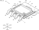
- FIG. 2 is a perspective view of a main part of the semiconductor device according to the first embodiment of the present disclosure.
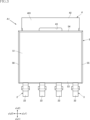
- FIG. 3 is a plan view showing the semiconductor device according to the first embodiment of the present disclosure.
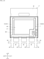
- FIG. 4 is a plan view showing a main part of the semiconductor device according to the first embodiment of the present disclosure.
- FIG. 5 is a bottom view showing the semiconductor device according to the first embodiment of the present disclosure.
- FIG. 6 is a bottom view of a main portion showing the semiconductor device according to the first embodiment of the present disclosure.
- FIG. 7 is a side view showing the semiconductor device according to the first embodiment of the present disclosure.
- FIG. 8 is a cross-sectional view taken along line VIII-VIII in FIG.
- FIG. 9 is a cross-sectional view taken along line IX-IX in FIG.
- FIG. 10 is a cross-sectional view taken along line XX in FIG.
- FIG. 11 is a partially enlarged view of FIG.
- FIG. 12 is a partially enlarged view of FIG.
- FIG. 13 is a plan view showing a process in the manufacture of the semiconductor device according to the first embodiment of the present disclosure.
- FIG. 14 is a plan view showing a step subsequent to that shown in FIG.
- FIG. 15 is a partially enlarged side view of the step shown in FIG.
- FIG. 16 is a partially enlarged side view showing a step subsequent to that shown in FIG.
- FIG. 17 is a plan view of a main portion showing a semiconductor device according to a second embodiment of the present disclosure.
- FIG. 18 is a cross-sectional view taken along line XVIII-XVIII in FIG.
- FIG. 19 is a partially enlarged view of FIG.
- FIG. 20 is a plan view of a main portion showing a semiconductor device according to a third embodiment of the present disclosure.
- an object A is formed on an object B" and “an object A is formed on an object B” include “an object A is formed directly on an object B” and “an object A is formed on an object B with another object interposed between the object A and the object B” unless otherwise specified.
- an object A is disposed on an object B” and “an object A is disposed on an object B” include “an object A is disposed directly on an object B” and “an object A is disposed on an object B with another object interposed between the object A and the object B" unless otherwise specified.
- an object A is located on an object B includes “an object A is located on an object B in contact with an object B” and “an object A is located on an object B with another object interposed between the object A and the object B” unless otherwise specified.
- an object A overlaps an object B when viewed in a certain direction includes “an object A overlaps the entire object B” and “an object A overlaps a part of an object B.”
- a surface A faces in direction B is not limited to the case where the angle of surface A with respect to direction B is 90 degrees, but also includes the case where surface A is tilted with respect to direction B.
- First embodiment: 1 to 12 show a semiconductor device according to a first embodiment of the present disclosure.
- the semiconductor device A1 of this embodiment includes a semiconductor element 1, a first conductive member 2, a second conductive member 3, a third conductive member 4, and a sealing resin 5.
- the semiconductor device A1 further includes a conductive bonding material 19, a first conductive bonding material 29, and a second conductive bonding material 39.
- the application of the semiconductor device A1 is not limited in any way, and it is used in electronic devices including a power conversion circuit, such as a DC-DC converter.
- FIG. 1 is a perspective view of the semiconductor device A1.
- FIG. 2 is a perspective view of the main part of the semiconductor device A1, omitting the sealing resin 5.
- FIG. 3 is a plan view of the semiconductor device A1.
- FIG. 4 is a plan view of the main part of the semiconductor device A1, seen through the sealing resin 5.
- FIG. 5 is a bottom view of the semiconductor device A1.
- FIG. 6 is a bottom view of the main part of the semiconductor device A1, seen through the sealing resin 5.
- FIG. 7 is a side view of the semiconductor device A1.
- FIG. 8 is a cross-sectional view taken along line VIII-VIII in FIG. 4.
- FIG. 9 is a cross-sectional view taken along line IX-IX in FIG. 4.
- FIG. 10 is a cross-sectional view taken along line X-X in FIG. 4.
- FIG. 11 is a partial enlarged view of FIG. 8.
- FIG. 12 is a partial enlarged view of FIG. 9.
- FIG. 4 is a partial enlarged view. Note that in FIG. 4 and FIG. 6, the sealing resin 5 seen through is shown by an imaginary line (two-dot chain line).
- an example of the thickness direction is the "thickness direction z".
- the direction perpendicular to the thickness direction z (the up-down direction in Figures 3 and 4) is an example of the first direction and is called the "first direction x".
- the direction perpendicular to the thickness direction z and the first direction x (the left-right direction in Figures 3 and 4) is an example of the second direction and is called the "second direction y”.
- the lower side in the figure is an example of "one side of the first direction” and is called the "x1 side of the first direction x”
- the upper side in the figure is an example of "the other side of the first direction” and is called the "x2 side of the first direction x".
- the semiconductor element 1 is an element that exerts the electrical function of the semiconductor device A1.
- the semiconductor element 1 is a three-terminal element having three electrodes, for example a MOSFET (Metal-Oxide-Semiconductor Field-Effect Transistor).
- the semiconductor element 1 may be a switching element such as an IGBT (Insulated Gate Bipolar Transistor) or a diode.
- the semiconductor element 1 is an n-channel type MOSFET with a vertical structure.
- the semiconductor element 1 is rectangular when viewed in the thickness direction z.
- the semiconductor element 1 has a first element surface 101, a second element surface 102, a first electrode 11, a second electrode 12, and a third electrode 13.
- the first element surface 101 and the second element surface 102 are spaced apart in the thickness direction z and face opposite each other.
- the first element surface 101 faces the z1 side in the thickness direction z.
- the second element surface 102 faces the z2 side in the thickness direction z.
- the first electrode 11 is disposed on the first surface 101 of the element. A current corresponding to the power converted by the semiconductor element 1 flows through the first electrode 11. In other words, the first electrode 11 corresponds to the source electrode of the semiconductor element 1.
- the second electrode 12 is disposed on the first surface 101 of the element.
- a gate voltage for driving the semiconductor element 1 is applied to the second electrode 12.
- the second electrode 12 corresponds to the gate electrode of the semiconductor element 1.
- the area of the second electrode 12 is smaller than the area of the first electrode 11.
- the third electrode 13 is disposed on the first surface 101 of the element. A current corresponding to the power before being converted by the semiconductor element 1 flows through the third electrode 13. In other words, the third electrode 13 corresponds to the drain electrode of the semiconductor element 1.
- the first conductive member 2 includes a portion that is disposed on the z1 side of the semiconductor element 1 in the thickness direction z.
- the first conductive member 2 includes a conductive material such as metal, and is made of, for example, a metal plate material.
- the constituent material of the first conductive member 2 includes, for example, Cu (copper).
- the first conductive member 2 is a metal plate material that is appropriately bent. As shown in Figures 1 to 6 and 8 to 10, the first conductive member 2 has a pad portion 21 and multiple terminal portions 22.
- the pad portion 21 is a portion that is conductively joined to the first electrode 11 of the semiconductor element 1. There are no limitations on the shape or size of the pad portion 21, and in the illustrated example, the pad portion 21 is shaped to overlap most of the first electrode 11 when viewed in the thickness direction z, and also to expose the second electrode 12.
- the pad portion 21 has a first main surface 211 and a first back surface 212.
- the first main surface 211 is a surface facing the z1 side in the thickness direction z.
- the first back surface 212 is a surface facing the z2 side in the thickness direction z.
- the first back surface 212 of the pad portion 21 is bonded to the first electrode 11 of the semiconductor element 1 via the first conductive bonding material 29.
- the pad portion 21 and the first electrode 11 are conductively bonded to each other via the first conductive bonding material 29.
- the material of the first conductive bonding material 29 is not particularly limited, and may be, for example, solder (a metal containing tin and silver).
- the first conductive bonding material 29 may also be made of a metal paste containing a metal such as silver (Ag).
- the distance between the first electrode 11 and the first back surface 212 in the thickness direction z (first distance d1) is, for example, 5 ⁇ m or more and 30 ⁇ m or less.
- a plating layer made of, for example, silver (Ag) may be formed on the area of the pad portion 21 that is bonded to the semiconductor element 1 (first electrode 11).
- the multiple terminals 22 are connected to the pad 21 on the x1 side in the first direction x.
- the terminals 22 each extend in the first direction x when viewed in the thickness direction z, and are arranged at intervals in the second direction y.
- the number of the multiple terminals 22 is not limited, and may be three as in the illustrated example, or may be two, four or more. Also, a configuration may be provided with only one terminal 22.
- the terminal 22 has a portion connected to the pad 21 and covered with the sealing resin 5, a portion protruding from the sealing resin 5 to the x1 side in the first direction x, a portion folded back to the z2 side in the thickness direction z, and a portion located on the z2 side in the thickness direction z.
- the multiple terminals 22 are used as terminals when mounting the semiconductor device A1.
- the multiple terminals 22 are electrically connected to the first electrode 11 of the semiconductor element 1.
- the multiple terminals 22 are source terminals of the semiconductor device A1.
- a plating layer made of an alloy mainly composed of tin (Sn), for example, may be formed on the portion of the first conductive member 2 (multiple terminal portions 22) exposed from the sealing resin 5.
- the second conductive member 3 includes a portion that is disposed on the z1 side of the semiconductor element 1 in the thickness direction z.
- the second conductive member 3 includes a conductive material such as metal, and is made of, for example, a metal plate material.
- the material that makes up the second conductive member 3 includes, for example, Cu (copper).
- the second conductive member 3 is a metal plate material that is appropriately bent. As shown in Figures 1 to 7, 9, and 12, the second conductive member 3 has a first pad portion 31, a terminal portion 32, a first bent portion 33, and a second bent portion 34.
- the first pad portion 31 is a portion that is conductively joined to the second electrode 12 of the semiconductor element 1. There are no limitations on the shape or size of the first pad portion 31, and in the illustrated example, it is shaped to overlap a portion of the second electrode 12 when viewed in the thickness direction z, and also to expose the second electrode 12.
- the first pad portion 31 has a second main surface 311 and a second back surface 312.
- the second main surface 311 is a surface facing the z1 side in the thickness direction z.
- the second back surface 312 is a surface facing the z2 side in the thickness direction z.
- the area of the second back surface 312 is smaller than the area of the first back surface 212 of the pad portion 21 in the first conductive member 2.
- the first bent portion 33 is connected to the x1 side of the first direction x with respect to the first pad portion 31.
- the first bent portion 33 is inclined so as to be located on the z1 side of the thickness direction z as it approaches the x1 side of the first direction x.
- the second bent portion 34 is connected to the x2 side of the first direction x with respect to the first pad portion 31.
- the second bent portion 34 is inclined so as to be located on the z1 side of the thickness direction z as it approaches the x2 side of the first direction x.
- the inclination angle ⁇ 1 of the first bent portion 33 with respect to the first direction x and the inclination angle ⁇ 2 of the second bent portion 34 with respect to the first direction x are the same.
- the inclination angle ⁇ 1 and the inclination angle ⁇ 2 are the same” means that the inclination angle ⁇ 1 and the inclination angle ⁇ 2 are the same in design, and includes cases where the inclination angle ⁇ 1 and the inclination angle ⁇ 2 are different due to manufacturing errors, etc.
- the inclination angles ⁇ 1 and ⁇ 2 are not particularly limited, but in the illustrated example, the inclination angles ⁇ 1 and ⁇ 2 are approximately 45°.
- the first pad portion 31, the first bent portion 33, and the second bent portion 34 are bonded to the second electrode 12 of the semiconductor element 1 via the second conductive bonding material 39.
- the first pad portion 31, the first bent portion 33, and the second bent portion 34 are conductively bonded to the second electrode 12 via the second conductive bonding material 39.
- the second conductive bonding material 39 includes a thin portion 391, a first portion 392, and a second portion 393.
- the thin portion 391 is interposed between the second electrode 12 and the second back surface 312 in the thickness direction z, and is a portion that contacts the second electrode 12 and the second back surface 312.
- the first portion 392 is located on the x1 side of the thin portion 391 in the first direction x, and is a portion that contacts the second electrode 12 and the first bent portion 33.
- the second portion 393 is located on the x2 side of the thin portion 391 in the first direction x, and is in contact with the second electrode 12 and the second bent portion 34.
- the distance (second distance d2) between the second electrode 12 and the second back surface 312 in the thickness direction z is smaller than the distance (first distance d1) between the first electrode 11 and the first back surface 212 in the thickness direction z.
- the second distance d2 between the second electrode 12 and the second back surface 312 in the thickness direction z is, for example, 1 ⁇ m or more and 20 ⁇ m or less.
- the second electrode 12 and the second back surface 312 may be in partial contact.
- the ratio of the first distance d1 between the first electrode 11 and the first back surface 212 in the thickness direction z to the dimension t1 in the thickness direction z from the second back surface 312 to the second main surface 311 is, for example, 0.5% or more and 10% or less.
- the dimension t1 is, for example, about 0.1 mm or more and 1 mm or less.
- the constituent material of the second conductive bonding material 39 is not particularly limited, and may be, for example, solder (a metal containing tin and silver).
- the second conductive bonding material 39 may also be made of a metal paste containing a metal such as silver (Ag). Note that a plating layer made of, for example, silver (Ag) may be formed on the areas of the first pad portion 31, the first bent portion 33, and the second bent portion 34 that are bonded to the semiconductor element 1 (second electrode 12).
- the terminal portion 32 is connected to the first bent portion 33 on the x1 side in the first direction x.
- the terminal portion 32 extends in the first direction x when viewed in the thickness direction z.
- the terminal portion 32 has a portion connected to the first bent portion 33 and covered with the sealing resin 5, a portion protruding from the sealing resin 5 to the x1 side in the first direction x, a portion folded back to the z2 side in the thickness direction z, and a portion located on the z2 side in the thickness direction z.
- the terminal portion 32 When viewed in the second direction y, the terminal portion 32 has a shape and size that roughly overlaps with the terminal portion 22.
- the terminal portion 32 is used as a terminal when mounting the semiconductor device A1.
- the terminal portion 32 is electrically connected to the second electrode 12 of the semiconductor element 1.
- the terminal portion 32 is a gate terminal of the semiconductor device A1.
- a plating layer made of an alloy mainly composed of tin (Sn), for example, may be formed on the portion of the second conductive member 3 (terminal portion 32) exposed from the sealing resin 5.
- the third conductive member 4 is disposed on the z2 side of the semiconductor element 1 in the thickness direction z.
- the third conductive member 4 includes a conductive material such as a metal, for example, copper (Cu).
- the third conductive member 4 has a main surface 401 and a back surface 402.
- the main surface 401 faces the z1 side in the thickness direction z.
- the back surface 402 faces the z2 side in the thickness direction z.
- the semiconductor element 1 is mounted on the main surface 401.
- the back surface 402 is exposed from the sealing resin 5.
- the third conductive member 4 has an island portion 41, a terminal portion 42, and a through hole 43.
- the island portion 41 is a portion on which the entire or part of the semiconductor element 1 is mounted.
- the island portion 41 includes a part of the main surface 401 and a part of the back surface 402. There are no limitations on the shape or size of the island portion 41, and in the illustrated example, it is substantially rectangular when viewed in the thickness direction z.
- the island portion 41 has a first edge portion 411, a second edge portion 412, a third edge portion 413, and a groove 414.
- the first edge portion 411 is located on the y1 side of the second direction y and extends in the first direction x.
- the second edge portion 412 is located on the y2 side of the second direction y and extends in the first direction x.
- the third edge portion 413 is located on the x1 side of the first direction x and extends in the second direction y.
- the groove 414 is recessed from the main surface 401 to the z2 side of the thickness direction z, and has a generally V-shaped cross section.
- the groove 414 surrounds the semiconductor element 1 when viewed in the thickness direction z.
- Each of the first edge portion 411, the second edge portion 412, the third edge portion 413, and the groove 414 is covered with the sealing resin 5.
- the island portion 41 may be configured without the recessed groove 414.
- the first edge portion 411 has a first step portion 411a, as shown in Figures 4 and 6.
- the first step portion 411a is formed on the x2 side of the first direction x relative to the semiconductor element 1 in the first direction x.
- the first step portion 411a is shaped so that the x2 side of the first direction x is recessed toward the y2 side of the second direction y relative to the x1 side of the first direction x.
- the first step portion 411a is inclined with respect to the first direction x and the second direction y so that it is positioned on the y2 side of the second direction y as it approaches the x2 side of the first direction x in the first direction x.
- the second edge portion 412 has a second step portion 412a.
- the second step portion 412a is formed on the x2 side of the first direction x relative to the semiconductor element 1 in the first direction x.
- the second step portion 412a is shaped so that the x2 side of the first direction x is recessed toward the y1 side of the second direction y relative to the x1 side of the first direction x.
- the second step portion 412a is inclined with respect to the first direction x and the second direction y so that it is positioned on the y1 side of the second direction y as it approaches the x2 side of the first direction x in the first direction x.
- the island portion 41 includes a main portion 41A, a first thin portion 41B, and a second thin portion 41C, as shown in Figures 4, 6, and 10.
- the main portion 41A has a portion of the main surface 401 and a portion of the back surface 402.
- the first thin portion 41B is a portion that is connected to the y1 side of the main portion 41A in the second direction y.
- the first thin portion 41B has a part of the main surface 401 and a first intermediate surface 403.
- the first thin portion 41B is a portion that does not have a back surface 402.
- the first intermediate surface 403 faces the z2 side in the thickness direction z.
- the first intermediate surface 403 is located between the main surface 401 and the back surface 402 in the thickness direction z.
- the first thin portion 41B has a shape that is recessed on the z2 side in the thickness direction z with respect to the main portion 41A.
- the first thin portion 41B includes the entire first edge portion 411.
- the first step portion 411a is formed in the first thin portion 41B.
- the second thin portion 41C is a portion that is connected to the y2 side of the main portion 41A in the second direction y.
- the second thin portion 41C has a part of the main surface 401 and a second intermediate surface 404.
- the second thin portion 41C is a portion that does not have a back surface 402.
- the second intermediate surface 404 faces the z2 side of the thickness direction z.
- the second intermediate surface 404 is located between the main surface 401 and the back surface 402 in the thickness direction z.
- the second thin portion 41C has a shape that is recessed on the z2 side of the thickness direction z with respect to the main portion 41A.
- the second thin portion 41C includes the entire second edge portion 412.
- the second step portion 412a is formed in the second thin portion 41C.
- the semiconductor element 1 overlaps the main portion 41A and the first thin portion 41B when viewed in the thickness direction z. Also, the semiconductor element 1 overlaps the main portion 41A and the second thin portion 41C when viewed in the thickness direction z.
- the semiconductor element 1 is bonded to the main surface 401 of the island portion 41 via a conductive bonding material 19.
- the second element surface 102 of the semiconductor element 1 faces the main surface 401.
- the third electrode 13 on the second element surface 102 and the main surface 401 are conductively bonded via the conductive bonding material 19.
- the material of the conductive bonding material 19 is not particularly limited, and may be, for example, solder (a metal containing tin and silver).
- the conductive bonding material 19 may also be made of a metal paste containing a metal such as silver (Ag).
- a plating layer made of, for example, silver (Ag) may be formed on the area of the main surface 401 of the island portion 41 where the semiconductor element 1 is bonded.
- the terminal portion 42 is a portion that is connected to the x2 side of the island portion 41 in the first direction x.
- the terminal portion 42 includes a portion of the main surface 401 and a portion of the back surface 402.
- the terminal portion 42 may be used as a terminal when mounting the semiconductor device A1.
- the terminal portion 42 is electrically connected to the third electrode 13 of the semiconductor element 1.
- the terminal portion 42 is a drain terminal of the semiconductor device A1.
- the through hole 43 penetrates the third conductive member 4 in the thickness direction z.
- the through hole 43 is filled with a portion of the sealing resin 5.
- the size of the cross section of the through hole 43 perpendicular to the thickness direction z is larger on the z2 side of the thickness direction z than on the z1 side of the thickness direction z. This has the effect of, for example, preventing the third conductive member 4 from falling off the sealing resin 5.
- a plating layer made of an alloy mainly composed of tin (Sn), for example, may be formed on the portion of the third conductive member 4 exposed from the sealing resin 5.
- the sealing resin 5 covers the semiconductor element 1 and a portion of each of the first conductive member 2, the second conductive member 3, and the third conductive member 4.
- the sealing resin 5 has electrical insulation properties.
- the sealing resin 5 includes, for example, a black epoxy resin containing a filler.
- the shape of the sealing resin 5 is not limited in any way.
- the sealing resin 5 of this embodiment has a first resin surface 51, a second resin surface 52, a third resin surface 53, a fourth resin surface 54, a fifth resin surface 55, and a sixth resin surface 56, as shown in Figures 1 and 3 to 10.
- the first resin surface 51 faces the z1 side in the thickness direction z.
- the second resin surface 52 faces the z2 side in the thickness direction z.
- the back surface 402 of the third conductive member 4 is exposed from the second resin surface 52.
- the first resin surface 51 and the second resin surface 52 are flat surfaces, but are not limited to this and may be curved or bent surfaces, for example.
- the second resin surface 52 and the back surface 402 are flush with each other.
- the third resin surface 53 is a surface facing the x1 side in the first direction x.
- the fourth resin surface 54 is a surface facing the x2 side in the first direction x.
- the third resin surface 53 and the fourth resin surface 54 are slightly curved surfaces, but are not limited to this and may be curved surfaces or flat surfaces, for example.
- a plurality of terminal portions 22 and terminal portion 32 protrude from the third resin surface 53, and terminal portion 42 protrudes from the fourth resin surface 54.
- the fifth resin surface 55 is a surface facing the y1 side in the second direction y.
- the sixth resin surface 56 is a surface facing the y2 side in the second direction y.
- the fifth resin surface 55 and the sixth resin surface 56 are slightly curved surfaces, but are not limited to this and may be, for example, curved surfaces or flat surfaces.
- Figures 13 and 14 are plan views showing a step in the manufacture of the semiconductor device A1.
- Figure 15 is a partially enlarged side view of the step shown in Figure 14.
- Figure 16 is a partially enlarged side view showing the step following Figure 15.
- FIGS. 14 and 15 show a state in which the first bonding layer 929 and the second bonding layer 939 are disposed on the semiconductor element 1 mounted on the third conductive member 4.
- the first bonding layer 929 and the first bonding layer 929 will later become the first conductive bonding material 29 and the second conductive bonding material 39, and are, for example, solder paste applied by a dispenser.
- a metal clip member 90 is disposed on the z1 side of the thickness direction z of the semiconductor element 1.
- the metal clip member 90 has a first conductive portion 92 and a second conductive portion 93 that are connected to each other.
- the first conductive portion 92 and the second conductive portion 93 are portions that will later become the first conductive member 2 and the second conductive member 3, and have a configuration in which adjacent terminal portions 22 are connected to each other and adjacent terminal portions 22 and terminal portions 32 are connected to each other by connecting portions 94.
- the first back surface 212 of the first conductive portion 92 (pad portion 21) overlaps the first bonding layer 929 when viewed in the thickness direction z.
- the second back surface 312 of the second conductive portion 93 (first pad portion 31) overlaps the second bonding layer 939 when viewed in the thickness direction z. Also, as shown in FIG.
- the first back surface 212 of the first conductive portion 92 (pad portion 21) is located on the z2 side in the thickness direction z from the second back surface 312 of the second conductive portion 93 (first pad portion 31).
- the distance between the first back surface 212 and the second back surface 312 in the thickness direction z is, for example, about 1 ⁇ m or more and 20 ⁇ m or less. Note that in FIG. 15 and FIG. 16 described later, the second bonding layer 939 is hatched for understanding.
- the metal clip member 90 is pressed against the semiconductor element 1 toward the z2 side in the thickness direction z (see arrow N1), while the first bonding layer 929 and the second bonding layer 939 are heated, melted, and solidified.
- the metal clip member 90 is pressed against the z2 side in the thickness direction z until the second back surface 312 receives a reaction force from the second electrode 12 (see arrow N2).
- the second bonding layer 939 interposed between the second electrode 12 and the second back surface 312 is pushed out to the periphery, and a thin portion 9391, a first portion 9392, and a second portion 9393 are formed.
- the distance between the second electrode 12 and the second back surface 312 is smaller than the distance between the first electrode 11 and the first back surface 212.
- the sealing resin 5 is formed, and the connecting portion 94 and the like are appropriately cut to separate the multiple terminal portions 22 and the terminal portions 32 from each other.
- the multiple terminal portions 22 and the terminal portions 32 are subjected to bending processing. In this way, the first conductive member 2 and the second conductive member 3 are formed.
- the semiconductor device A1 includes a first conductive adhesive 29 and a second conductive adhesive 39.
- the first conductive adhesive 29 is interposed between the first electrode 11 and the first back surface 212 of the first conductive member 2, and is bonded to the first electrode 11 and the first conductive member 2.
- the second conductive adhesive 39 is interposed between the second electrode 12 and the second back surface 312 of the second conductive member 3, and is bonded to the second electrode 12 and the second conductive member 3.
- the area of the second back surface 312 is smaller than the area of the first back surface 212.
- the distance (second distance d2) between the second electrode 12 and the second back surface 312 in the thickness direction z is smaller than the distance (first distance d1) between the first electrode 11 and the first back surface 212 in the thickness direction z.
- the second conductive member 3 includes a first pad portion 31 having a second back surface 312, a first bent portion 33, and a second bent portion 34.
- the first bent portion 33 is connected to the x1 side of the first direction x with respect to the first pad portion 31, and is located on the z1 side of the thickness direction z as it moves toward the x1 side of the first direction x.
- the second bent portion 34 is connected to the x2 side of the first direction x with respect to the first pad portion 31, and is located on the z1 side of the thickness direction z as it moves toward the x2 side of the first direction x.
- the second conductive bonding material 39 includes a first portion 392 that contacts the second electrode 12 and the first bent portion 33, and a second portion 393 that contacts the second electrode 12 and the second bent portion 34.
- the bonding state between the second electrode 12 and the second conductive member 3 (the first pad portion 31, the first bent portion 33, and the second bent portion 34) is more stable with reduced bias, which is more suitable for improving bonding reliability.
- the inclination angle ⁇ 1 of the first bent portion 33 with respect to the first direction x and the inclination angle ⁇ 2 of the second bent portion 34 with respect to the first direction x are the same. This allows the first portion 392 in contact with the first bent portion 33 and the second portion 393 in contact with the second bent portion 34 to be formed more evenly in the first direction x. This is preferable in terms of improving the bonding reliability of the semiconductor device A1.
- FIGS. 17 to 20 show other embodiments of the present disclosure.
- elements that are the same as or similar to those in the above embodiment are given the same reference numerals as in the above embodiment, and duplicated explanations will be omitted.
- the configurations of the parts in each embodiment can be combined with each other as appropriate to the extent that no technical contradictions arise.
- FIG. 17 is a plan view of a main part of a semiconductor device A2 according to this embodiment, seen through the sealing resin 5.
- Fig. 18 is a cross-sectional view taken along line XVIII-XVIII in Fig. 17.
- Fig. 19 is a partially enlarged view of Fig. 18.
- the see-through sealing resin 5 is shown by an imaginary line (two-dot chain line).
- the semiconductor device A2 further includes a fourth conductive member 6 and a third conductive bonding material 69, and accordingly has been modified as appropriate compared to the semiconductor device A1.
- the pad portion 21 of the first conductive member 2 exposes a portion of the first electrode 11 (the corner portion on the x1 side in the first direction x and the y1 side in the second direction y).
- the first conductive member 2 includes two terminal portions 22.
- the fourth conductive member 6 is disposed apart from the second conductive member 3 in the second direction y. In this embodiment, the fourth conductive member 6 is disposed between the first conductive member 2 (terminal portion 22) and the second conductive member 3 in the second direction y.
- the fourth conductive member 6 includes a portion disposed on the z1 side of the semiconductor element 1 in the thickness direction z.
- the fourth conductive member 6 includes a conductive material such as metal, and is formed, for example, of a metal plate material.
- the constituent material of the fourth conductive member 6 includes, for example, Cu (copper).
- the fourth conductive member 6 is a metal plate material that is appropriately bent.
- the fourth conductive member 6 has a second pad portion 61, a terminal portion 62, a third bend portion 63, and a third bend portion 63.
- the second pad portion 61 is a portion that is conductively joined to the first electrode 11 of the semiconductor element 1. There are no limitations on the shape or size of the second pad portion 61, and in the illustrated example, it is shaped to overlap a portion of the first electrode 11 when viewed in the thickness direction z, and to expose the first electrode 11.
- the second pad portion 61 has a third main surface 611 and a third back surface 612.
- the third main surface 611 is a surface facing the z1 side in the thickness direction z.
- the third back surface 612 is a surface facing the z2 side in the thickness direction z.
- the area of the third back surface 612 is smaller than the area of the first back surface 212 of the pad portion 21 in the first conductive member 2.
- the third bend 63 is connected to the x1 side of the first direction x with respect to the second pad portion 61.
- the third bend 63 is inclined to be located on the z1 side of the thickness direction z as it approaches the x1 side of the first direction x.
- the fourth bend 64 is connected to the x2 side of the first direction x with respect to the second pad portion 61.
- the fourth bend 64 is inclined to be located on the z1 side of the thickness direction z as it approaches the x2 side of the first direction x.
- the inclination angle ⁇ 3 of the third bend 63 with respect to the first direction x and the inclination angle ⁇ 4 of the fourth bend 64 with respect to the first direction x are the same.
- the inclination angle ⁇ 3 and the inclination angle ⁇ 4 are the same.
- the inclination angle ⁇ 3 and the inclination angle ⁇ 4 are the same in design, and includes cases where the inclination angle ⁇ 3 and the inclination angle ⁇ 4 are different due to manufacturing errors, etc.
- the inclination angles ⁇ 3 and ⁇ 4 are not particularly limited, but in the illustrated example, the inclination angles ⁇ 3 and ⁇ 4 are approximately 45°.
- the second pad portion 61, the third bend portion 63, and the fourth bend portion 64 are bonded to the first electrode 11 of the semiconductor element 1 via a third conductive bonding material 69.
- the second pad portion 61, the third bend portion 63, and the fourth bend portion 64 are conductively bonded to the first electrode 11 via the third conductive bonding material 69.
- the third conductive bonding material 69 includes a thin portion 691, a third portion 692, and a fourth portion 693.
- the thin portion 691 is interposed between the first electrode 11 and the third back surface 612 in the thickness direction z, and is a portion that contacts the first electrode 11 and the third back surface 612.
- the third portion 692 is located on the x1 side of the thin portion 691 in the first direction x, and is a portion that contacts the first electrode 11 and the third bend portion 63.
- the fourth portion 693 is located on the x2 side of the thin portion 691 in the first direction x, and is in contact with the first electrode 11 and the fourth bent portion 64.
- the distance (third distance d3) between the first electrode 11 and the third back surface 612 in the thickness direction z is smaller than the distance (first distance d1) between the first electrode 11 and the first back surface 212 in the thickness direction z (see FIG. 11).
- the third distance d3 between the first electrode 11 and the third back surface 612 in the thickness direction z is, for example, 1 ⁇ m or more and 20 ⁇ m or less.
- the first electrode 11 and the third back surface 612 may be in partial contact.
- the constituent material of the third conductive bonding material 69 is not particularly limited, and may be, for example, solder (a metal containing tin and silver).
- the third conductive bonding material 69 may also be made of a metal paste containing a metal such as silver (Ag).
- a plating layer made of, for example, silver (Ag) may be formed on the areas of the second pad portion 61, the third bend portion 63, and the fourth bend portion 64 that are bonded to the semiconductor element 1 (first electrode 11).
- the terminal portion 62 is connected to the third bent portion 63 on the x1 side in the first direction x.
- the terminal portion 62 extends in the first direction x when viewed in the thickness direction z.
- the terminal portion 62 has a portion connected to the third bent portion 63 and covered by the sealing resin 5, a portion protruding from the sealing resin 5 to the x1 side in the first direction x, a portion folded back to the z2 side in the thickness direction z, and a portion located on the z2 side in the thickness direction z.
- the terminal portion 62 When viewed in the second direction y, the terminal portion 62 has a shape and size that generally overlaps with the terminal portion 22 and the terminal portion 32.
- the terminal portion 62 is used as a terminal when mounting the semiconductor device A1.
- the terminal portion 62 is electrically connected to the first electrode 11 of the semiconductor element 1.
- the terminal portion 62 is a source sense terminal of the semiconductor device A1.
- the semiconductor device A2 of this embodiment can be manufactured in the same manner as described above with reference to Figures 13 to 16 with respect to the manufacturing direction of the semiconductor device A1 of the above embodiment.
- the semiconductor device A2 has the same effect as the semiconductor device A1 described above.
- the semiconductor device A2 further includes a fourth conductive member 6 and a third conductive bonding material 69.
- the third conductive bonding material 69 is interposed between the first electrode 11 and the third back surface 612 of the fourth conductive member 6, and is bonded to the first electrode 11 and the fourth conductive member 6.
- the area of the third back surface 612 is smaller than the area of the first back surface 212.
- the distance (third distance d3) between the first electrode 11 and the third back surface 612 in the thickness direction z is smaller than the distance (first distance d1) between the first electrode 11 and the first back surface 212 in the thickness direction z.
- the fourth conductive member 6 includes a second pad portion 61 having a third back surface 612, a third bent portion 63, and a fourth bent portion 64.
- the third bent portion 63 is connected to the x1 side of the first direction x with respect to the second pad portion 61, and is located on the z1 side of the thickness direction z as it moves toward the x1 side of the first direction x.
- the fourth bent portion 64 is connected to the x2 side of the first direction x with respect to the second pad portion 61, and is located on the z1 side of the thickness direction z as it moves toward the x2 side of the first direction x.
- the third conductive bonding material 69 includes a third portion 692 that contacts the first electrode 11 and the third bent portion 63, and a fourth portion 693 that contacts the first electrode 11 and the fourth bent portion 64.
- the bonding state between the first electrode 11 and the fourth conductive member 6 (the second pad portion 61, the third bent portion 63, and the fourth bent portion 64) is more stable with reduced bias, which is more suitable for improving bonding reliability.
- the inclination angle ⁇ 3 of the third bent portion 63 with respect to the first direction x is the same as the inclination angle ⁇ 4 of the fourth bent portion 64 with respect to the first direction x. This allows the third portion 692 in contact with the third bent portion 63 and the fourth portion 693 in contact with the fourth bent portion 64 to be formed more evenly in the first direction x. This is preferable in terms of improving the bonding reliability of the semiconductor device A2.
- Fig. 20 shows a semiconductor device according to a third embodiment of the present disclosure.
- Fig. 20 is a plan view of a main part of a semiconductor device A3 according to the present embodiment, seen through the sealing resin 5.
- the seen-through sealing resin 5 is shown by an imaginary line (two-dot chain line).
- the semiconductor device A3 of this embodiment includes a fourth conductive member 6 and a third conductive bonding material 69, similar to the semiconductor device A2 described above.
- the semiconductor device A3 differs from the semiconductor device A2 in the arrangement of the fourth conductive member 6.
- the fourth conductive member 6 is arranged on the y2 side of the second direction y, and is located on the opposite side of the first conductive member 2 from the second conductive member 3 in the second direction y.
- the specific configuration of the fourth conductive member 6 and the third conductive bonding material 69 is similar to that of the semiconductor device A2 described above.
- the semiconductor device A3 of this embodiment can be manufactured in the same manner as described above with reference to Figures 13 to 16 regarding the manufacturing direction of the semiconductor device A1 of the above embodiment.
- the semiconductor device A3 has the same effects as the semiconductor device A1 and the semiconductor device A2 described above.
- the semiconductor device according to the present disclosure is not limited to the above-mentioned embodiment.
- the specific configuration of each part of the semiconductor device according to the present disclosure can be freely designed in various ways.
- Appendix 1 a semiconductor element having a first electrode and a second electrode disposed on one side in a thickness direction; a first conductive member located on one side of the first electrode in the thickness direction and having a first back surface facing the other side in the thickness direction; a second conductive member located on one side of the second electrode in the thickness direction and having a second back surface facing the other side in the thickness direction; a first conductive bonding material interposed between the first electrode and the first back surface and bonded to the first electrode and the first conductive member; a second conductive bonding material interposed between the second electrode and the second back surface and bonded to the second electrode and the second conductive member;
- the area of the second back surface is smaller than the area of the first back surface, a second distance between the second electrode and the second back surface in the thickness direction is smaller than a first distance between the first electrode and the first back surface in the thickness direction.
- the second conductive member includes a first pad portion having the second back surface, a first bent portion connected to one side of the first pad portion in a first direction perpendicular to the thickness direction and positioned toward one side of the thickness direction as it approaches the one side of the first direction, and a second bent portion connected to the other side of the first pad portion in the first direction and positioned toward the other side of the thickness direction as it approaches the other side of the first direction,
- the semiconductor device described in Appendix 1 wherein the second conductive bonding material includes a first portion in contact with the second electrode and the first bent portion, and a second portion in contact with the second electrode and the second bent portion.
- an inclination angle of the first bent portion with respect to the first direction is equal to an inclination angle of the second bent portion with respect to the first direction.
- Appendix 4. 4. The semiconductor device according to claim 1, wherein a constituent material of the first conductive bonding material and a constituent material of the second conductive bonding material include solder.
- Appendix 5. the first conductive member and the second conductive member are made of a metal plate, the second conductive member has a second main surface that overlaps the second back surface when viewed in the thickness direction and faces one side in the thickness direction, 5.
- a ratio of the first distance to a dimension in the thickness direction from the second back surface to the second main surface is 0.5% or more and 10% or less.
- Appendix 6 The semiconductor device according to claim 5, wherein a constituent material of the first conductive member and a constituent material of the second conductive member include copper. Appendix 7. 7. The semiconductor device according to claim 1, wherein the first distance is greater than or equal to 5 ⁇ m and less than or equal to 30 ⁇ m. Appendix 8. 8. The semiconductor device according to claim 1, further comprising a sealing resin that covers the semiconductor element and at least a portion of each of the first conductive member and the second conductive member. Appendix 9. Further comprising a third conductive member; the semiconductor element has a third electrode disposed on the other side in the thickness direction, 9.
- the semiconductor device is a switching element having a drain electrode, a source electrode, and a gate electrode; 10. The semiconductor device according to claim 9, wherein the first electrode is the source electrode, the second electrode is the gate electrode, and the third electrode is the drain electrode. Appendix 11.
- a fourth conductive member having a third back surface located on one side of the first electrode in the thickness direction and facing the other side in the thickness direction; a third conductive bonding material interposed between the first electrode and the third back surface and bonded to the first electrode and the fourth conductive member, an area of the third back surface is smaller than an area of the first back surface; 11.
- a third distance between the first electrode and the third back surface in the thickness direction is smaller than the first distance.
- the fourth conductive member includes a second pad portion having the third back surface, a third bent portion connected to one side of the second pad portion in the first direction and positioned on one side in the thickness direction as it approaches the one side in the first direction, and a fourth bent portion connected to the other side of the second pad portion in the first direction and positioned on the other side in the thickness direction as it approaches the other side in the first direction, 12.
- the third conductive bonding material includes a third portion in contact with the first electrode and the third bent portion, and a fourth portion in contact with the first electrode and the fourth bent portion. Appendix 13. 13.
- the first conductive portion has a first back surface that overlaps the first bonding layer when viewed in the thickness direction and faces the other side in the thickness direction;
- the second conductive portion has a second back surface that overlaps the second bonding layer when viewed in the thickness direction and faces the other side in the thickness direction, the second back surface is located on the other side in the thickness direction than the first back surface,
- A1, A2, A3, A4, A5 semiconductor device 1: semiconductor element 101: element first surface 102: element second surface 11: first electrode 12: second electrode 13: third electrode 19: conductive bonding material 2: first conductive member 21: pad portion 211: first main surface 212: first back surface 22: terminal portion 29: first conductive bonding material 3: second conductive member 31: first pad portion 311: second main surface 312: second back surface 32: terminal portion 33: first bent portion 34: second bent portion 39: second conductive bonding material 391: thin portion 392: first portion 393: second portion 4: third conductive member 401: main surface 402: back surface 403: first intermediate surface 404: second intermediate surface 41: island portion 41A: Main portion 41B: First thin portion 41C: Second thin portion 411: First edge portion 411a: First step portion 412: Second edge portion 412a: Second step portion 413: Third edge portion 414: Groove 42: Terminal portion 43: Through hole 5: Sealing resin 51: First resin surface 52: Second resin surface 53: Third resin
Landscapes
- Structures Or Materials For Encapsulating Or Coating Semiconductor Devices Or Solid State Devices (AREA)
Priority Applications (2)
| Application Number | Priority Date | Filing Date | Title |
|---|---|---|---|
| JP2025526000A JPWO2024252845A1 (https=) | 2023-06-08 | 2024-05-10 | |
| US19/404,938 US20260101798A1 (en) | 2023-06-08 | 2025-12-01 | Semiconductor device and method for producing semiconductor device |
Applications Claiming Priority (2)
| Application Number | Priority Date | Filing Date | Title |
|---|---|---|---|
| JP2023-094659 | 2023-06-08 | ||
| JP2023094659 | 2023-06-08 |
Related Child Applications (1)
| Application Number | Title | Priority Date | Filing Date |
|---|---|---|---|
| US19/404,938 Continuation US20260101798A1 (en) | 2023-06-08 | 2025-12-01 | Semiconductor device and method for producing semiconductor device |
Publications (1)
| Publication Number | Publication Date |
|---|---|
| WO2024252845A1 true WO2024252845A1 (ja) | 2024-12-12 |
Family
ID=93795292
Family Applications (1)
| Application Number | Title | Priority Date | Filing Date |
|---|---|---|---|
| PCT/JP2024/017398 Ceased WO2024252845A1 (ja) | 2023-06-08 | 2024-05-10 | 半導体装置、および半導体装置の製造方法 |
Country Status (3)
| Country | Link |
|---|---|
| US (1) | US20260101798A1 (https=) |
| JP (1) | JPWO2024252845A1 (https=) |
| WO (1) | WO2024252845A1 (https=) |
Citations (4)
| Publication number | Priority date | Publication date | Assignee | Title |
|---|---|---|---|---|
| US20080036078A1 (en) * | 2006-08-14 | 2008-02-14 | Ciclon Semiconductor Device Corp. | Wirebond-less semiconductor package |
| US20090212284A1 (en) * | 2008-02-22 | 2009-08-27 | Infineon Technologies Ag | Electronic device and manufacturing thereof |
| US20100072585A1 (en) * | 2008-09-25 | 2010-03-25 | Alpha & Omega Semiconductor Incorporated | Top exposed clip with window array |
| WO2019064775A1 (ja) * | 2017-09-29 | 2019-04-04 | 日立金属株式会社 | 半導体装置およびその製造方法 |
-
2024
- 2024-05-10 JP JP2025526000A patent/JPWO2024252845A1/ja active Pending
- 2024-05-10 WO PCT/JP2024/017398 patent/WO2024252845A1/ja not_active Ceased
-
2025
- 2025-12-01 US US19/404,938 patent/US20260101798A1/en active Pending
Patent Citations (4)
| Publication number | Priority date | Publication date | Assignee | Title |
|---|---|---|---|---|
| US20080036078A1 (en) * | 2006-08-14 | 2008-02-14 | Ciclon Semiconductor Device Corp. | Wirebond-less semiconductor package |
| US20090212284A1 (en) * | 2008-02-22 | 2009-08-27 | Infineon Technologies Ag | Electronic device and manufacturing thereof |
| US20100072585A1 (en) * | 2008-09-25 | 2010-03-25 | Alpha & Omega Semiconductor Incorporated | Top exposed clip with window array |
| WO2019064775A1 (ja) * | 2017-09-29 | 2019-04-04 | 日立金属株式会社 | 半導体装置およびその製造方法 |
Also Published As
| Publication number | Publication date |
|---|---|
| JPWO2024252845A1 (https=) | 2024-12-12 |
| US20260101798A1 (en) | 2026-04-09 |
Similar Documents
| Publication | Publication Date | Title |
|---|---|---|
| US7800206B2 (en) | Semiconductor device | |
| CN1499622A (zh) | 引线框及制造方法以及树脂密封型半导体器件及制造方法 | |
| JP7649171B2 (ja) | 半導体装置 | |
| JP7845824B2 (ja) | 半導体装置 | |
| JP2009038139A (ja) | 半導体装置およびその製造方法 | |
| CN114551395A (zh) | 半导体封装结构及其制造方法 | |
| US20220301967A1 (en) | Semiconductor device | |
| JP2009164240A (ja) | 半導体装置 | |
| US20220301966A1 (en) | Semiconductor device | |
| JP2008294219A (ja) | 半導体装置及びその製造方法 | |
| WO2024252845A1 (ja) | 半導体装置、および半導体装置の製造方法 | |
| WO2026094683A1 (ja) | 半導体装置 | |
| US20240047315A1 (en) | Semiconductor device | |
| US20240170353A1 (en) | Semiconductor device and mounting structure for semiconductor element | |
| WO2025027936A1 (ja) | 半導体装置、電力変換装置、及びその製造方法 | |
| WO2024176851A1 (ja) | 半導体装置 | |
| WO2024128062A1 (ja) | 半導体装置 | |
| WO2025154469A1 (ja) | 半導体装置、および半導体装置の製造方法 | |
| WO2024252830A1 (ja) | 半導体装置および車両 | |
| JP2025145847A (ja) | 半導体装置、および、半導体装置の製造方法 | |
| WO2025063004A1 (ja) | 電子装置および電子装置の製造方法 | |
| WO2024116899A1 (ja) | 半導体装置、および半導体装置の製造方法 | |
| WO2025018112A1 (ja) | 半導体装置 | |
| JP2025166930A (ja) | 半導体装置および半導体装置の製造方法 | |
| WO2025017953A1 (ja) | 半導体装置 |
Legal Events
| Date | Code | Title | Description |
|---|---|---|---|
| 121 | Ep: the epo has been informed by wipo that ep was designated in this application |
Ref document number: 24819082 Country of ref document: EP Kind code of ref document: A1 |
|
| ENP | Entry into the national phase |
Ref document number: 2025526000 Country of ref document: JP Kind code of ref document: A |
|
| WWE | Wipo information: entry into national phase |
Ref document number: 2025526000 Country of ref document: JP |
|
| NENP | Non-entry into the national phase |
Ref country code: DE |