WO2024252661A1 - 半導体装置 - Google Patents
半導体装置 Download PDFInfo
- Publication number
- WO2024252661A1 WO2024252661A1 PCT/JP2023/021509 JP2023021509W WO2024252661A1 WO 2024252661 A1 WO2024252661 A1 WO 2024252661A1 JP 2023021509 W JP2023021509 W JP 2023021509W WO 2024252661 A1 WO2024252661 A1 WO 2024252661A1
- Authority
- WO
- WIPO (PCT)
- Prior art keywords
- wiring
- power supply
- line
- substrate
- wiring layer
- Prior art date
- Legal status (The legal status is an assumption and is not a legal conclusion. Google has not performed a legal analysis and makes no representation as to the accuracy of the status listed.)
- Ceased
Links
Images






Classifications
-
- H—ELECTRICITY
- H10—SEMICONDUCTOR DEVICES; ELECTRIC SOLID-STATE DEVICES NOT OTHERWISE PROVIDED FOR
- H10W—GENERIC PACKAGES, INTERCONNECTIONS, CONNECTORS OR OTHER CONSTRUCTIONAL DETAILS OF DEVICES COVERED BY CLASS H10
- H10W20/00—Interconnections in chips, wafers or substrates
- H10W20/40—Interconnections external to wafers or substrates, e.g. back-end-of-line [BEOL] metallisations or vias connecting to gate electrodes
- H10W20/41—Interconnections external to wafers or substrates, e.g. back-end-of-line [BEOL] metallisations or vias connecting to gate electrodes characterised by their conductive parts
- H10W20/43—Layouts of interconnections
-
- H—ELECTRICITY
- H10—SEMICONDUCTOR DEVICES; ELECTRIC SOLID-STATE DEVICES NOT OTHERWISE PROVIDED FOR
- H10D—INORGANIC ELECTRIC SEMICONDUCTOR DEVICES
- H10D84/00—Integrated devices formed in or on semiconductor substrates that comprise only semiconducting layers, e.g. on Si wafers or on GaAs-on-Si wafers
-
- H—ELECTRICITY
- H10—SEMICONDUCTOR DEVICES; ELECTRIC SOLID-STATE DEVICES NOT OTHERWISE PROVIDED FOR
- H10D—INORGANIC ELECTRIC SEMICONDUCTOR DEVICES
- H10D84/00—Integrated devices formed in or on semiconductor substrates that comprise only semiconducting layers, e.g. on Si wafers or on GaAs-on-Si wafers
- H10D84/01—Manufacture or treatment
- H10D84/02—Manufacture or treatment characterised by using material-based technologies
- H10D84/03—Manufacture or treatment characterised by using material-based technologies using Group IV technology, e.g. silicon technology or silicon-carbide [SiC] technology
- H10D84/038—Manufacture or treatment characterised by using material-based technologies using Group IV technology, e.g. silicon technology or silicon-carbide [SiC] technology using silicon technology, e.g. SiGe
-
- H—ELECTRICITY
- H10—SEMICONDUCTOR DEVICES; ELECTRIC SOLID-STATE DEVICES NOT OTHERWISE PROVIDED FOR
- H10W—GENERIC PACKAGES, INTERCONNECTIONS, CONNECTORS OR OTHER CONSTRUCTIONAL DETAILS OF DEVICES COVERED BY CLASS H10
- H10W20/00—Interconnections in chips, wafers or substrates
- H10W20/40—Interconnections external to wafers or substrates, e.g. back-end-of-line [BEOL] metallisations or vias connecting to gate electrodes
- H10W20/41—Interconnections external to wafers or substrates, e.g. back-end-of-line [BEOL] metallisations or vias connecting to gate electrodes characterised by their conductive parts
- H10W20/42—Vias, e.g. via plugs
Definitions
- the present invention relates to a semiconductor device.
- a technology that provides a power switch circuit that switches between supplying and cutting off power to transistors.
- a known technology is BS-PDN (Backside Power Delivery Network) that provides a power line on the back side of a semiconductor substrate and supplies power to transistors provided on the front side of the semiconductor substrate through vias such as TSVs (Through Silicon Vias).
- BS-PDN Backside Power Delivery Network
- TSVs Through Silicon Vias
- a known technology is that directly connects vias from the back side of the semiconductor substrate to the sources and drains of transistors provided on the front side of the semiconductor substrate.
- the present invention was made in consideration of the above points, and aims to suppress an increase in circuit area when a power switch circuit is provided on the back surface of a board.
- a semiconductor device in one aspect of the present invention, includes a substrate, a first power supply line formed below an upper surface of the substrate and supplied with a first potential, a second power supply line supplied with a second potential, a first control line formed below an upper surface of the substrate, a first transistor formed below an upper surface of the substrate and electrically provided between the first power supply line and the second power supply line, the first transistor having a gate electrically connected to the first control line, a semiconductor layer formed on the substrate, a tap cell formed on the substrate and disposed in a position overlapping the semiconductor layer and the first control line in a plan view, the tap cell having a via connected to the semiconductor layer and the first control line, and a control circuit formed on the substrate and electrically connected to the via.
- the disclosed technology makes it possible to suppress an increase in circuit area when a power switch circuit is provided on the back surface of a substrate.
- FIG. 7 is a cross-sectional view showing an example of a cross section taken along line X1-X1' and line X2-X2' in FIG. 6. 7 is a cross-sectional view showing another example of a cross section taken along the line X1-X1' in FIG. 6.
- FIG. 6 is a plan view showing a first modified example of the layout of the circuits and wirings shown in FIGS. 4 and 5 .
- FIG. 6 is a plan view showing a second modified example of the layout of the circuits and wiring shown in FIGS. 4 and 5 .
- FIG. 6 is a plan view showing a third modified example of the layout of the circuits and wirings shown in FIGS. 4 and 5 .
- FIG. 12 is a cross-sectional view showing an example of a cross section taken along line X3-X3' and line X4-X4' in FIG. 11.
- 13 is a plan view showing an example of a layout of circuits and wiring of a standard cell block in a semiconductor device according to a second embodiment
- FIG. 13 is a plan view showing an outline of the layout of circuits and wirings of a standard cell block in a semiconductor device according to a third embodiment
- 13 is a cross-sectional view showing an example of a layout of circuits and wiring of a standard cell block in a semiconductor device according to a fourth embodiment;
- the symbols indicating signals are also used to indicate signal lines or signal terminals.
- the symbols indicating power supply potential are also used to indicate power supply lines or power supply terminals to which the power supply potential is supplied.
- First Embodiment Fig. 1 shows an example of a layout of a semiconductor device according to the first embodiment.
- the semiconductor device 100 shown in Fig. 1 may be a SoC (System on Chip) or a standalone FPGA (Field-Programmable Gate Array).
- the semiconductor device 100 has a plurality of I/O cells IOC, IOCP and an internal circuit region INTR.
- the I/O cell IOC is an interface circuit for a signal SGNL such as an input signal, an output signal, or an input/output signal.
- the I/O cell IOCP is an interface circuit for a power supply potential or a ground potential.
- Each I/O cell IOC, IOCP is connected to an internal circuit region INTR.
- the internal circuit region INTR has one or more standard cell blocks SCB in which standard cells are provided.
- the internal circuit region INTR may also be equipped with logic circuits other than standard cells, or with memory.
- the memory may be equipped within the standard cell block SCB.
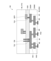
- FIG. 2 shows an example of a cross-sectional structure of the semiconductor device 100 of FIG. 1.
- the semiconductor device 100 has a substrate SUB, a wiring layer WL1 formed on the front surface FS side of the substrate SUB, and a wiring layer WL2 formed on the back surface BS side of the substrate SUB.
- the front surface FS of the substrate SUB is an example of the upper surface of the substrate SUB or the upper side of the substrate SUB
- the back surface BS of the substrate SUB is an example of the lower side of the substrate SUB.
- a fin FIN which is a part of a transistor, is formed on the front surface of the substrate SUB.
- the fin FIN has a source, drain, and channel.
- a pad PAD which is an external connection terminal, is formed on the surface (back surface) of the wiring layer WL2 opposite the substrate SUB.
- the wiring layer WL2 has multiple wiring layers BSM1 and BSM2 (two layers in FIG. 2, BSM stands for Backside Metal).
- BSM1 and BSM2 are formed with wiring W1 and W2, respectively, which supply power supply potential and ground potential, etc.
- the wiring W1 and W2 are connected to each other through a via VIA1.
- the wiring W2 and the pad PAD are connected to each other through a via VIA2.
- the wiring W1 is connected to the source and drain of the fin FIN via a TSV formed in the substrate SUB.
- the wiring W1 may be connected to a buried wiring BPR (Buried Power Rail) buried in the surface of the substrate SUB via the TSV.
- BPR Buried Power Rail
- the TSV is an example of a via.
- the transistors formed on the substrate SUB are not limited to finFETs (Field Effect Transistors) using fins.
- the transistors formed on the substrate SUB may be planar MOSFETs (Metal Oxide Semiconductor FETs), nanosheet FETs, or complementary FETs (CFETs).
- planar MOSFETs and nanosheet FETs the TSVs that supply the power supply potential or ground potential are connected to the source and drain of the transistor.
- the TSVs that supply the power supply potential or ground potential may be connected to the source and drain that are located closest to the substrate SUB.
- FIG. 3 shows an example of a circuit arranged in the standard cell block SCB of FIG. 1.
- the standard cell block SCB has a power switch circuit PSW and a standard cell SC.
- the standard cell SC is connected to a virtual power line VVDD and a ground line VSS, and operates by receiving a supply of a virtual power potential VVDD from the virtual power line VVDD.
- the power switch circuit PSW has a control circuit CNTL and a switch transistor SWT.
- the control circuit CNTL is a buffer circuit having inverters IV1 and IV2 connected in series between an input signal line IN and an output signal line OUT. Each inverter IV1 and IV2 operates while connected to a power supply line TVDD and a ground line VSS.
- the inverter IV1 inverts the logic of the input signal IN and outputs it as an output signal OUT0.
- the inverter IV2 inverts the logic of the output signal OUT0 from the inverter IV1 and outputs it as an output signal OUT.
- the switch transistor SWT is a PMOS transistor with its source connected to the power supply line TVDD and its drain connected to the virtual power supply line VVDD, and operates by receiving the voltage of the output signal OUT0 from the control circuit CNTL as its gate potential. While the switch transistor SWT is on, the power supply line TVDD and the virtual power supply line VVDD are electrically connected, and the power supply potential TVDD is supplied to the standard cell SC via the virtual power supply line VVDD.
- the switch transistor SWT While the switch transistor SWT is off, the electrical connection between the power supply line TVDD and the virtual power supply line VVDD is cut off, and the virtual power supply line VVDD is set to a floating state.
- the input IN of the inverter IV1 or the output OUT of the inverter IV2 may be connected to the gate of the switch transistor SWT. This is similar to the other embodiments.
- the control circuit CNTL may be arranged in a region separate from the region in which the power switch circuit PSW is arranged.
- the output signal OUT may be supplied to an input terminal IN of another power switch circuit PSW.
- the switch transistor SWT is an example of a first transistor that is provided below the upper surface of the substrate SUB and is electrically provided between the power line TVDD and the virtual power line VVDD.
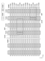
- Figure 4 shows an overview of the layout of the circuits and wiring in Figure 3.
- Figure 4 shows, in plan view, the wiring FS (Front Side) on the front side of the substrate SUB, the wiring in the PR (Power Rail) layer provided within the substrate SUB, the wiring in the wiring layer BSM1 provided on the back side of the substrate SUB, and the positions of the control circuit CNTL and the signal tap cell STAP.
- FS Front Side
- PR Power Rail
- wiring extending in the Y direction (power supply line TVDD, ground line VSS, virtual power supply line VVDD, signal line SIG) is arranged side by side in the X direction.
- the ground line VSS extending in the Y direction is interrupted halfway, and the signal line SIG is arranged at the interrupted position.
- the signal line SIG is arranged between multiple ground lines VSS in the Y direction.
- the output signal OUT0 output from inverter IV1 in FIG. 3 is transmitted to the signal line SIG.
- the signal line SIG of the wiring layer PR is an example of a first control line.
- the power supply line TVDD of the wiring layer PR is an example of a first power supply line
- the power supply potential TVDD is an example of a first potential.
- the virtual power supply line VVDD of the wiring layer PR is an example of a second power supply line
- the virtual power supply potential VVDD is an example of a second potential.
- the ground line VSS of the wiring layer PR is an example of a third power supply line.
- the control circuit CNTL is arranged in a position overlapping the area in which the power supply line TVDD and the ground line VSS of the wiring layer PR are arranged in a plan view.
- the signal tap cell STAP is arranged in a position overlapping the area in which the signal line SIG of the wiring layer PR is arranged in a plan view.
- control circuit CNTL and the signal tap cell STAP may be placed at separate locations or adjacent to each other as shown in FIG. 4.
- the control circuit CNTL may be placed in a power domain (constant power domain) where the power supply potential TVDD is constantly supplied
- the signal tap cell STAP may be placed in a power domain (power cutoff domain) where the supply of the virtual power supply potential VVDD can be stopped.
- the wiring of the wiring layer BSM1 (virtual power line VVDD, power line TVDD, ground line VSS, signal line SIG) is arranged below the wiring layer PR.
- Each wiring of the wiring layer BSM1 extends in the X direction and is arranged side by side in the Y direction.
- wiring of the same type for example, VSS and VSS, or TVDD and TVDD
- the control circuit CNTL and the signal tap cell STAP are mutually connected by wiring FS.
- FIG. 5 shows an overview of the layout of the circuits and wiring in FIG. 3 on another layer.
- FIG. 5 shows an area that overlaps with FIG. 4 in plan view, and shows the wiring of the wiring layers BSM1 and BSM2 provided on the back side of the substrate SUB, as well as the positions of the signal tap cell STAP and the switch transistor SWT, among the circuits and wiring in FIG. 3.
- Each wiring (virtual power line VVDD, power line TVDD, etc.) in the wiring layer BSM2 extends in the Y direction and is arranged side by side in the X direction.
- the switch transistor SWT is arranged in a position adjacent to the signal tap cell STAP in a planar view.
- the signal tap cell STAP and the switch transistor SWT may be arranged in positions separated from each other in a planar view.
- FIG. 5 shows only the layers on the back side of the substrate SUB, the position of the control circuit CNTL is omitted, but the position of the control circuit CNTL is the same as in FIG. 4.
- the type of wiring in the wiring layer BSM2 that overlaps with the control circuit CNTL in a plan view is not limited to the power supply line TVDD and ground line VSS of the wiring layer PR shown in FIG. 4.
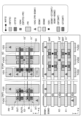
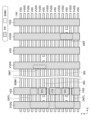
- FIG. 6 shows an example of the layout of the circuits and wiring shown in FIGS. 4 and 5.
- the layout shown in the upper part of FIG. 6 shows the layout above the wiring layer PR, excluding via VIA3.
- the layout shown in the lower part of FIG. 6 shows the layout below the substrate SUB.
- the symbol W (FS) indicates signal wiring provided on the surface side of the substrate SUB.
- the symbol DIF (FS) indicates a semiconductor layer such as a diffusion layer provided on the surface of the substrate.
- the symbol GT (FS) indicates a transistor gate provided on the surface side of the substrate.
- the symbol VIA4 indicates a via that connects the semiconductor layer DIF (FS) and the wiring of the wiring layer PR.
- the symbol PR indicates a wiring provided in the wiring layer PR.
- the symbol VIA3 indicates a via that connects the wiring of the wiring layer PR and the wiring of the wiring layer BSM1.
- the symbol BSM1 indicates a wiring provided in the wiring layer BSM1.
- the symbol BSM2 indicates a wiring provided in the wiring layer BSM2.
- the symbol VIA1 indicates a via that connects the wiring of the wiring layer BSM1 to the gate GT (SWT) of the switch transistor SWT, or a via that connects the wiring of the wiring layer BSM1 to the wiring of the wiring layer BSM2.
- the symbol DIF (SWT) indicates the semiconductor layer (diffusion layer) of the switch transistor SWT.
- the symbol GT (SWT) indicates the gate of the switch transistor SWT.
- a transistor including a semiconductor layer DIF (FS) and a gate GT (FS) is formed on the substrate SUB.
- the control circuit CNTL includes, for example, two stages of inverters IV1 and IV2 as shown in FIG. 3.
- the output of the first stage inverter IV1 is connected to the gate GT (SWT) of the switch transistor SWT via the wiring W (FS), the semiconductor layer DIF (FS) of the signal tap cell STAP, the via VIA4, the wiring SIG of the wiring layer PR, the via VIA3, the wiring SIG of the wiring layer BSM1, and the via VIA1.
- the PR layer wiring SIG is arranged in a region where the ground line VSS of the PR layer extending in the Y direction is interrupted midway and where the signal tap cell STAP is arranged.
- the PR layer ground line VSS is arranged to avoid the region where the signal tap cell STAP is arranged. This makes it possible to increase the area where the ground line VSS is arranged and reduce the ground resistance compared to the case where the PR layer wiring SIG extends uninterrupted in the Y direction.
- the transistors of the control circuit CNTL are, for example, fin-based field effect transistors (FinFETs), planar metal oxide semiconductor FETs (Metal Oxide Semiconductor FETs), nanosheet FETs, or complementary FETs (CFETs).
- a ground potential VSS or a power supply potential TVDD is supplied to the transistors of the control circuit CNTL from the wiring of the wiring layer PR through vias VIA4 that are directly connected to the source and drain, which are the semiconductor layers of the transistors.
- the switch transistor SWT is located in a region where the virtual power supply line VVDD and the ground line VSS of the wiring layer PR are arranged in a plan view, and overlaps with a standard cell SC (e.g., an inverter) in a plan view. Also, the switch transistor SWT is arranged between the wiring layer BSM1 and the wiring layer BSM2, as shown in FIG. 7.
- SC e.g., an inverter
- the control circuit CNTL is located in the area where the power supply line TVDD and the ground line VSS of the wiring layer PR are arranged.
- the wiring of the wiring layer PR connected to the control circuit CNTL and the wiring of the wiring layer PR connected to the signal tap cell STAP may be arranged with a gap between them as shown in FIG. 6, or may be arranged adjacent to each other.
- the via such as a TSV in an area on the front surface side of the substrate SUB where no transistors are provided.
- the via must be formed in an area separate from the circuit area (transistor area), which may result in an increase in the circuit area.
- a signal tap cell STAP is provided in the circuit area on the front side of the substrate SUB where the transistor is provided, using a via VIA4 that is directly connected from the back side of the substrate SUB to the semiconductor layer such as the source or drain of the transistor. Therefore, even when the switch transistor SWT is disposed on the back side of the substrate SUB, the signal SIG from the control circuit CNTL can be supplied to the gate of the switch transistor SWT without providing a separate area from the circuit area, thereby suppressing an increase in the circuit area.
- the signal SIG (output signal OUT0) is supplied from the control circuit CNTL to the gate GT (SWT) of the switch transistor SWT using the wiring W provided on the front side of the substrate SUB and the wiring in the BSM1 layer. This allows the control circuit CNTL and the switch transistor SWT to be placed at separate positions in a plan view.
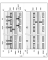
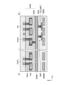
- FIG. 7 shows an example of a cross section along lines X1-X1' and X2-X2' in FIG. 6.
- the semiconductor layers (source, drain) of inverters IV1 and IV2 of the control circuit CNTL are connected to the power supply line TVDD or ground line VSS of the wiring layer PR through a via VIA4 formed in the substrate SUB.
- the wiring layer PR is arranged along the lower surface of the substrate SUB in FIG. 7, it may also be arranged in the substrate SUB.
- the wiring SIG that transmits the output signal OUT output from the control circuit CNTL is connected from the signal tap cell STAP through a via VIA4, a wiring layer PR, and a via VIA3 to the wiring SIG of the wiring layer BSM1.
- the wiring SIG of the wiring layer BSM1 is connected to the gate GT (SWT) of the switch transistor SWT through a via VIA1 formed in the interlayer insulating film below the wiring layer BSM1.
- the gate GT (SWT) is provided at a position facing the channel of the switch transistor SWT via the gate insulating film GINS.
- the source and drain of the switch transistor SWT provided on both sides of the channel in the X direction are respectively connected to the power supply line TVDD and the virtual power supply line VVDD formed in the wiring layer BSM2.
- the virtual power line VVDD of the wiring layer BSM2 which is connected to the power line TVDD via the switch transistor SWT, is connected to the virtual power line VVDD of the wiring layer BSM1 via a via VIA1 in the cross section along the X2-X2' line.
- the virtual power line VVDD of BSM1 is connected to the virtual power line VVDD of the wiring layer PR via a via VIA3.
- the virtual power line VVDD of the wiring layer PR is further connected to the semiconductor layer DIF (FS) of the standard cell SC or the power terminal of the standard cell SC via a via VIA4 in the cross section along the X1-X1' line.
- FIG. 8 shows another example of a cross section taken along line X1-X1' in FIG. 6. Elements and layouts that are the same as or similar to those in FIG. 7 are indicated with the same symbols or the same patterns, and detailed descriptions are omitted.
- the example shown in FIG. 8 is similar to the cross section taken along line X1-X1' in FIG. 7, except that the wiring of the wiring layer PR is formed in the substrate SUB, and the wiring of the wiring layer BSM1 is formed in a position that contacts the rear surface of the substrate SUB. Note that the structure in which the wiring of the wiring layer PR is formed in the substrate SUB can also be applied to other embodiments or modified examples.
- FIG. 9 shows a first modified example of the circuit and wiring layout shown in FIGS. 4 and 5. Elements and layouts that are the same as or similar to those in FIG. 6 are indicated by the same reference numerals or patterns, and detailed descriptions are omitted.
- FIG. 9 is similar to the layout of FIG. 6, except that the signal tap cell STAP is located adjacent to the control circuit CNTL.
- the signal tap cell STAP may be located in a power domain to which the power supply potential TVDD is constantly supplied together with the control circuit CNTL.
- FIG. 9 shows an example in which two switch transistors SWT are arranged, four switch transistors SWT may be arranged as in FIG. 6, or one, three, or five or more switch transistors SWT may be arranged.
- the layout shown in FIG. 9 may also be applied to other embodiments or modified examples.
- FIG. 10 shows a second modified example of the circuit and wiring layout shown in FIGS. 4 and 5. Elements and layouts that are the same as or similar to those in FIG. 6 are indicated with the same symbols or the same patterns, and detailed descriptions are omitted. Of the regions shown in FIG. 6, FIG. 10 shows only the region in which the switch transistor SWT is arranged, and the layout above the wiring layer PR is omitted from the illustration.
- the gate GT (SWT) of the switch transistor SWT, the semiconductor layer DIF (SWT), and the gate insulating film GINS are arranged to extend in the wiring direction of the wiring layer BSM2. This allows a switch transistor SWT with a driving capability greater than the four switch transistors SWT in FIG. 6 to be arranged in an area of the same size as FIG. 6.
- the layout shown in FIG. 10 may be applied to other embodiments or modified examples.
- FIG. 11 shows a third modified example of the circuit and wiring layout shown in FIGS. 4 and 5. Elements and layouts that are the same as or similar to those in FIG. 6 are indicated with the same symbols or the same patterns, and detailed descriptions are omitted. Of the regions shown in FIG. 6, FIG. 11 shows only the region in which the switch transistor SWT is arranged. The layout shown in the upper part of FIG. 11 is similar to the layout shown in the upper part of FIG. 6.
- the layout shown in the lower part of FIG. 11 differs from the layout shown in the lower part of FIG. 6 in the type and order of wiring in the wiring layer BSM1.
- the switch transistor SWT is arranged between the wiring layers PR and BSM1. Note that the gate GT (SWT) of the switch transistor SWT is arranged on the wiring layer BSM1 side with respect to the semiconductor layer DIF (SWT), but in FIG. 11 it is shown as being arranged on the semiconductor layer DIF (SWT) to make the position of the gate GT (SWT) identifiable.
- FIG. 11 shows an example in which one switch transistor SWT is arranged, but multiple switch transistors SWT may be arranged as in the other examples.
- the drain (semiconductor layer DIF (SWT)) of the switch transistor SWT is connected to the virtual power line VVDD of the wiring layer PR through a via VIA3.
- the source (semiconductor layer DIF (SWT)) of the switch transistor SWT is connected to the power line TVDD of the wiring layer BSM1 through a via VIA5.
- the gate GT (SWT) of the switch transistor SWT is connected to the signal line SIG of the wiring layer BSM1 through a via VIA6.
- FIG. 12 shows an example of a cross section taken along lines X3-X3' and X4-X4' in FIG. 11. Elements and layouts that are the same as or similar to those in FIG. 7 are indicated with the same symbols or patterns, and detailed descriptions are omitted.
- the wiring in the wiring layer BSM2 is omitted in FIG. 12 because it is not connected to the switch transistor SWT.
- the cross-sectional structure of the switch transistor SWT differs from that of the switch transistor SWT in FIG. 7 in that it is upside down.
- the gate GT (SWT) of the switch transistor SWT is connected to the signal line SIG of the wiring layer BSM1 in the cross section along the X3-X3' line.
- the source and drain, which are the semiconductor layer DIF (SWT) of the switch transistor SWT, are connected to the power supply line TVDD of the wiring layer BSM1 and the virtual power supply line VVDD of the wiring layer PR in the cross section along the X4-X4' line, respectively.
- the drain (VVDD) of the switch transistor SWT is directly connected to the virtual power line VVDD of the wiring layer PR through the via VIA3.
- a ground line VSS can be provided in place of the virtual power line VVDD of the wiring layer BSM1 of FIG. 6. This allows, for example, the number of ground lines VSS of the wiring layer BSM1 to be increased compared to FIG. 6, and the ground resistance to be reduced. If a power line TVDD is provided in place of the virtual power line VVDD of the wiring layer BSM1 of FIG. 6, the power resistance can be reduced.
- the wiring and switch transistor SWT located on the back side of the substrate SUB may be formed by bonding another semiconductor chip to the back side of the substrate SUB.
- the wiring and switch transistor SWT located on the back side of the substrate SUB may be formed by performing wafer processes such as film formation, exposure processing, and etching on the back side of the substrate SUB.
- the layouts shown in Figures 11 and 12 may be applied to other embodiments or modified examples.
- a signal tap cell STAP is provided in the circuit area on the front side of the substrate SUB where the transistor is provided, using a via VIA4 that is directly connected from the back side of the substrate SUB to the semiconductor layer such as the source or drain of the transistor. Therefore, even when the switch transistor SWT is disposed on the back side of the substrate SUB, the signal SIG from the control circuit CNTL can be supplied to the gate of the switch transistor SWT without providing a separate area from the circuit area, and an increase in the circuit area can be suppressed.
- the wiring SIG of the PR layer By arranging the wiring SIG of the PR layer in an area where the ground line VSS of the PR layer extending in the Y direction is interrupted, the area in which the ground line VSS is arranged can be increased and the ground resistance can be reduced compared to when the wiring SIG extends uninterrupted in the Y direction.
- the signal SIG (output signal OUT0) is supplied from the control circuit CNTL to the gate GT (SWT) of the switch transistor SWT using wiring W provided on the front side of the substrate SUB and wiring in the BSM1 layer. This allows the control circuit CNTL and the switch transistor SWT to be placed at separate positions in a plan view.
- Second Embodiment 13 shows an example of the layout of the circuits and wiring of the standard cell block in the semiconductor device of the second embodiment.
- the same or similar elements and layout as those in FIG. 6 are indicated by the same symbols or the same patterns, and detailed description is omitted.
- the control circuit CNTL is formed in the region in FIG. 6 in which the standard cells SC are formed.
- the control circuit CNTL may be disposed in a power domain (power cutoff region) in which the supply of the virtual power supply potential VVDD can be stopped.
- the configuration of the control circuit CNTL is the same as that of the control circuit CNTL in FIG. 6.
- the wiring SIG that transmits the output signal OUT output from the control circuit CNTL is connected to the gate GT (SWT) of the switch transistor SWT via the wiring W (FS), the semiconductor layer DIF (FS) of the signal tap cell STAP, the via VIA4, the wiring SIG of the wiring layer PR, the wiring SIG of the wiring layer BSM1, and the via VIA1.
- the transistors of the inverters IV1 and IV2 of the control circuit CNTL are, for example, fin FETs using fins, planar MOSFETs, nanosheet FETs, or CFETs.
- the transistors of the inverters IV1 and IV2 of the control circuit CNTL are supplied with the ground potential VSS or the power supply potential TVDD from the wiring of the wiring layer PR through the via VIA4 that is directly connected to the source and drain, which are the semiconductor layers of the transistors.
- the power supply line TVDD is arranged between the signal line SIG and the ground line VSS of the wiring layer PR in the X direction, but for example, the signal line SIG may be arranged between the power supply line TVDD and the ground line VSS.
- the power supply line TVDD is arranged between the interrupted ground lines VSS in the Y direction
- the signal line SIG is arranged between the interrupted virtual power supply lines VVDD in the Y direction.
- the second embodiment can also achieve the same effects as the first embodiment. For example, by connecting the control circuit CNTL and the gate GT (PSW) of the switch transistor SWT via the signal tap cell STAP, it is possible to suppress an increase in the circuit area. Furthermore, in the second embodiment, the control circuit CNTL and the switch transistor SWT can be positioned so that they overlap in a plan view.
- PSW gate GT
- Third Embodiment 14 shows an outline of the layout of the circuits and wiring of a standard cell block in a semiconductor device according to the third embodiment. Elements and layouts that are the same as or similar to those in FIG. 4 are indicated by the same reference numerals or patterns, and detailed descriptions thereof will be omitted.
- FIG. 14 differs from FIG. 4 in that the signal line SIG of the control circuit CNTL is formed using the wiring layer BSM1, without using the wiring FS on the front side of the substrate SUB.
- the signal line SIG of the wiring layer BSM1 is disposed at a position that connects the control circuit CNTL and the switch transistor SWT in a plan view, and electrically connects the control circuit CNTL and the gate GT (SWT) of the switch transistor SWT.
- the third embodiment can also achieve the same effects as the first embodiment. For example, by connecting the control circuit CNTL and the gate GT (PSW) of the switch transistor SWT via the signal tap cell STAP, it is possible to suppress an increase in the circuit area. Furthermore, in the second embodiment, the control circuit CNTL and the switch transistor SWT can be positioned so that they overlap in a plan view.
- PSW gate GT
- the third embodiment by arranging the signal lines SIG only in necessary locations in the wiring layer BSM1, it is possible to arrange, for example, the ground line VSS in an area where the signal lines SIG are not arranged. Also, the wiring SIG on the front surface FS side of the substrate SUB can be omitted. This makes it possible to efficiently arrange the wiring of the wiring layer BSM1 and the wiring of the standard cells SC.
- Fourth Embodiment 15 shows an example of the layout of the circuits and wiring of a standard cell block in the semiconductor device of the fourth embodiment. Elements and layouts that are the same as or similar to those in FIG. 7 are indicated by the same reference numerals or patterns, and detailed description thereof will be omitted.
Landscapes
- Semiconductor Integrated Circuits (AREA)
- Design And Manufacture Of Integrated Circuits (AREA)
Abstract
Description
図1は、第1実施形態における半導体装置のレイアウトの一例を示す。例えば、図1に示す半導体装置100は、SoC(System on Chip)でもよく、単体のFPGA(Field-Programmable Gate Array)等でもよい。
図13は、第2実施形態の半導体装置におけるスタンダードセルブロックの回路及び配線のレイアウトの一例を示す。図6と同一又は同様の要素及びレイアウトについては、同じ符号又は同じパターンで示し、詳細な説明は省略する。この実施形態では、図6においてスタンダードセルSCが形成される領域に制御回路CNTLが形成される。例えば、制御回路CNTLは、仮想電源電位VVDDの供給が停止可能な電源ドメイン(電源遮断領域)に配置されてもよい。制御回路CNTLの構成は、図6の制御回路CNTLの構成と同様である。
図14は、第3実施形態の半導体装置におけるスタンダードセルブロックの回路及び配線のレイアウトの概要を示す。図4と同一又は同様の要素及びレイアウトについては、同じ符号又は同じパターンで示し、詳細な説明は省略する。
図15は、第4実施形態の半導体装置におけるスタンダードセルブロックの回路及び配線のレイアウトの一例を示す。図7と同一又は同様の要素及びレイアウトについては、同じ符号又は同じパターンで示し、詳細な説明は省略する。
BPR 埋め込み配線
BS 裏面
BSM1、BSM2 配線層
CNTL 制御回路
DIF 半導体層
FIN フィン
FS 表面
GINS ゲート絶縁膜
GT ゲート
IN 入力信号
INTR 内部回路領域
IOC、IOCP I/Oセル
IV1、IV2 インバータ
OUT、OUT0 出力信号
PAD パッド
PR 配線層
PSW 電源スイッチ回路
SC スタンダードセル
SCB スタンダードセルブロック
SGNL 信号
SIG 信号線
STAP 信号タップセル
SUB 基板
SWT スイッチトランジスタ
TVDD 電源線
VIA1、VIA2、VIA3、VIA4、VIA5、VIA6 ビア
VSS 接地線
VVDD 仮想電源線
W、W1、W2 配線
WL1、WL2 配線層
Claims (7)
- 基板と、
前記基板の上面より下方に形成され、第1の電位が供給される第1の電源線と、第2の電位が供給される第2の電源線と、
前記基板の上面より下方に形成された第1の制御線と、
前記基板の上面より下方に形成され、電気的に前記第1の電源線と前記第2の電源線との間に設けられ、前記第1の制御線に電気的に接続されたゲートを有する第1のトランジスタと、
前記基板上に形成された半導体層と、前記基板に形成され、平面視で前記半導体層と前記第1の制御線と重なる位置に配置され、前記半導体層及び前記第1の制御線に接続するビアと、を有するタップセルと、
前記基板上に形成され、前記ビアに電気的に接続する制御回路と、
を有する半導体装置。 - 平面視で第1の方向に延在して配置される複数の第3の電源線を有し、
前記第1の制御線は、前記第1の方向において前記複数の第3の電源線の間の領域に配置される
請求項1に記載の半導体装置。 - 前記制御回路及び前記第1のトランジスタは、平面視で離れて配置される
請求項1または請求項2に記載の半導体装置。 - 前記制御回路及び前記第1のトランジスタは、平面視で重なって配置される
請求項1または請求項2に記載の半導体装置。 - 前記第1の電源線、前記第2の電源線及び前記第1の制御線の下方で、平面視で前記第1の方向とは異なる第2の方向に延在する複数の第1の配線と、
前記第2の方向において前記複数の第1の配線の間に配置され、前記第1の制御線及び前記第1のトランジスタのゲートに電気的に接続される第2の制御線を有する
請求項2に記載の半導体装置。 - 前記第1の配線は、前記第3の電源線と電気的に接続される
請求項5に記載の半導体装置。 - 前記ビアは、前記第1のトランジスタの前記ゲートと平面視で重なって配置され、前記ゲートに直接接続される
請求項1に記載の半導体装置。
Priority Applications (4)
| Application Number | Priority Date | Filing Date | Title |
|---|---|---|---|
| JP2025525906A JPWO2024252661A1 (ja) | 2023-06-09 | 2023-06-09 | |
| PCT/JP2023/021509 WO2024252661A1 (ja) | 2023-06-09 | 2023-06-09 | 半導体装置 |
| CN202380099204.2A CN121312281A (zh) | 2023-06-09 | 2023-06-09 | 半导体装置 |
| US19/409,433 US20260107756A1 (en) | 2023-06-09 | 2025-12-04 | Semiconductor device |
Applications Claiming Priority (1)
| Application Number | Priority Date | Filing Date | Title |
|---|---|---|---|
| PCT/JP2023/021509 WO2024252661A1 (ja) | 2023-06-09 | 2023-06-09 | 半導体装置 |
Related Child Applications (1)
| Application Number | Title | Priority Date | Filing Date |
|---|---|---|---|
| US19/409,433 Continuation US20260107756A1 (en) | 2023-06-09 | 2025-12-04 | Semiconductor device |
Publications (1)
| Publication Number | Publication Date |
|---|---|
| WO2024252661A1 true WO2024252661A1 (ja) | 2024-12-12 |
Family
ID=93795567
Family Applications (1)
| Application Number | Title | Priority Date | Filing Date |
|---|---|---|---|
| PCT/JP2023/021509 Ceased WO2024252661A1 (ja) | 2023-06-09 | 2023-06-09 | 半導体装置 |
Country Status (4)
| Country | Link |
|---|---|
| US (1) | US20260107756A1 (ja) |
| JP (1) | JPWO2024252661A1 (ja) |
| CN (1) | CN121312281A (ja) |
| WO (1) | WO2024252661A1 (ja) |
Citations (4)
| Publication number | Priority date | Publication date | Assignee | Title |
|---|---|---|---|---|
| JP2021061278A (ja) * | 2019-10-03 | 2021-04-15 | 株式会社ソシオネクスト | 半導体集積回路装置 |
| WO2021075353A1 (ja) * | 2019-10-18 | 2021-04-22 | 株式会社ソシオネクスト | 半導体集積回路装置 |
| WO2022138324A1 (ja) * | 2020-12-25 | 2022-06-30 | 株式会社ソシオネクスト | 半導体集積回路装置 |
| WO2023054602A1 (ja) * | 2021-09-30 | 2023-04-06 | 株式会社ソシオネクスト | 半導体装置 |
-
2023
- 2023-06-09 CN CN202380099204.2A patent/CN121312281A/zh active Pending
- 2023-06-09 WO PCT/JP2023/021509 patent/WO2024252661A1/ja not_active Ceased
- 2023-06-09 JP JP2025525906A patent/JPWO2024252661A1/ja active Pending
-
2025
- 2025-12-04 US US19/409,433 patent/US20260107756A1/en active Pending
Patent Citations (4)
| Publication number | Priority date | Publication date | Assignee | Title |
|---|---|---|---|---|
| JP2021061278A (ja) * | 2019-10-03 | 2021-04-15 | 株式会社ソシオネクスト | 半導体集積回路装置 |
| WO2021075353A1 (ja) * | 2019-10-18 | 2021-04-22 | 株式会社ソシオネクスト | 半導体集積回路装置 |
| WO2022138324A1 (ja) * | 2020-12-25 | 2022-06-30 | 株式会社ソシオネクスト | 半導体集積回路装置 |
| WO2023054602A1 (ja) * | 2021-09-30 | 2023-04-06 | 株式会社ソシオネクスト | 半導体装置 |
Also Published As
| Publication number | Publication date |
|---|---|
| CN121312281A (zh) | 2026-01-09 |
| JPWO2024252661A1 (ja) | 2024-12-12 |
| US20260107756A1 (en) | 2026-04-16 |
Similar Documents
| Publication | Publication Date | Title |
|---|---|---|
| JP7160105B2 (ja) | 半導体装置 | |
| JP7315016B2 (ja) | 半導体装置 | |
| US12119339B2 (en) | Semiconductor integrated circuit device | |
| US12094882B2 (en) | Semiconductor integrated circuit device | |
| JP7639871B2 (ja) | 半導体装置 | |
| JP7529121B2 (ja) | 半導体装置 | |
| US20240421089A1 (en) | Semiconductor integrated circuit device | |
| WO2023054601A1 (ja) | 半導体装置 | |
| CN105609466B (zh) | 金属区段作为接着垫及ic装置中的区域互连件 | |
| US10777579B2 (en) | Semiconductor integrated circuit device | |
| WO2024252661A1 (ja) | 半導体装置 | |
| US20260033000A1 (en) | Semiconductor device | |
| WO2024214206A1 (ja) | 半導体装置 | |
| WO2025169464A1 (ja) | 半導体装置 | |
| US20260096419A1 (en) | Semiconductor device | |
| JP7848630B2 (ja) | 半導体装置 | |
| WO2025079229A1 (ja) | 半導体装置 | |
| WO2025079230A1 (ja) | 半導体装置 | |
| WO2025181961A1 (ja) | 半導体装置 | |
| WO2025079231A1 (ja) | 半導体装置 | |
| WO2025169463A1 (ja) | 半導体装置 | |
| WO2025181960A1 (ja) | 半導体装置 | |
| WO2025079232A1 (ja) | 半導体装置 | |
| CN212517203U (zh) | 基本数字逻辑单元、集成电路版图及半导体器件 | |
| WO2025079233A1 (ja) | 半導体装置 |
Legal Events
| Date | Code | Title | Description |
|---|---|---|---|
| 121 | Ep: the epo has been informed by wipo that ep was designated in this application |
Ref document number: 23940759 Country of ref document: EP Kind code of ref document: A1 |
|
| ENP | Entry into the national phase |
Ref document number: 2025525906 Country of ref document: JP Kind code of ref document: A |
|
| WWE | Wipo information: entry into national phase |
Ref document number: CN2023800992042 Country of ref document: CN Ref document number: 2025525906 Country of ref document: JP |
|
| NENP | Non-entry into the national phase |
Ref country code: DE |