WO2024252660A1 - 半導体装置 - Google Patents
半導体装置 Download PDFInfo
- Publication number
- WO2024252660A1 WO2024252660A1 PCT/JP2023/021508 JP2023021508W WO2024252660A1 WO 2024252660 A1 WO2024252660 A1 WO 2024252660A1 JP 2023021508 W JP2023021508 W JP 2023021508W WO 2024252660 A1 WO2024252660 A1 WO 2024252660A1
- Authority
- WO
- WIPO (PCT)
- Prior art keywords
- power supply
- supply line
- transistor
- power
- substrate
- Prior art date
- Legal status (The legal status is an assumption and is not a legal conclusion. Google has not performed a legal analysis and makes no representation as to the accuracy of the status listed.)
- Ceased
Links
Images


Classifications
-
- H—ELECTRICITY
- H10—SEMICONDUCTOR DEVICES; ELECTRIC SOLID-STATE DEVICES NOT OTHERWISE PROVIDED FOR
- H10W—GENERIC PACKAGES, INTERCONNECTIONS, CONNECTORS OR OTHER CONSTRUCTIONAL DETAILS OF DEVICES COVERED BY CLASS H10
- H10W20/00—Interconnections in chips, wafers or substrates
- H10W20/40—Interconnections external to wafers or substrates, e.g. back-end-of-line [BEOL] metallisations or vias connecting to gate electrodes
- H10W20/41—Interconnections external to wafers or substrates, e.g. back-end-of-line [BEOL] metallisations or vias connecting to gate electrodes characterised by their conductive parts
- H10W20/427—Power or ground buses
-
- H—ELECTRICITY
- H02—GENERATION; CONVERSION OR DISTRIBUTION OF ELECTRIC POWER
- H02M—APPARATUS FOR CONVERSION BETWEEN AC AND AC, BETWEEN AC AND DC, OR BETWEEN DC AND DC, AND FOR USE WITH MAINS OR SIMILAR POWER SUPPLY SYSTEMS; CONVERSION OF DC OR AC INPUT POWER INTO SURGE OUTPUT POWER; CONTROL OR REGULATION THEREOF
- H02M7/00—Conversion of AC power input into DC power output; Conversion of DC power input into AC power output
- H02M7/42—Conversion of DC power input into AC power output without possibility of reversal
- H02M7/44—Conversion of DC power input into AC power output without possibility of reversal by static converters
- H02M7/48—Conversion of DC power input into AC power output without possibility of reversal by static converters using discharge tubes with control electrode or semiconductor devices with control electrode
- H02M7/53—Conversion of DC power input into AC power output without possibility of reversal by static converters using discharge tubes with control electrode or semiconductor devices with control electrode using devices of a triode or transistor type requiring continuous application of a control signal
- H02M7/537—Conversion of DC power input into AC power output without possibility of reversal by static converters using discharge tubes with control electrode or semiconductor devices with control electrode using devices of a triode or transistor type requiring continuous application of a control signal using semiconductor devices only, e.g. single switched pulse inverters
-
- H—ELECTRICITY
- H10—SEMICONDUCTOR DEVICES; ELECTRIC SOLID-STATE DEVICES NOT OTHERWISE PROVIDED FOR
- H10D—INORGANIC ELECTRIC SEMICONDUCTOR DEVICES
- H10D84/00—Integrated devices formed in or on semiconductor substrates that comprise only semiconducting layers, e.g. on Si wafers or on GaAs-on-Si wafers
- H10D84/01—Manufacture or treatment
- H10D84/02—Manufacture or treatment characterised by using material-based technologies
- H10D84/03—Manufacture or treatment characterised by using material-based technologies using Group IV technology, e.g. silicon technology or silicon-carbide [SiC] technology
- H10D84/038—Manufacture or treatment characterised by using material-based technologies using Group IV technology, e.g. silicon technology or silicon-carbide [SiC] technology using silicon technology, e.g. SiGe
-
- H—ELECTRICITY
- H10—SEMICONDUCTOR DEVICES; ELECTRIC SOLID-STATE DEVICES NOT OTHERWISE PROVIDED FOR
- H10W—GENERIC PACKAGES, INTERCONNECTIONS, CONNECTORS OR OTHER CONSTRUCTIONAL DETAILS OF DEVICES COVERED BY CLASS H10
- H10W20/00—Interconnections in chips, wafers or substrates
- H10W20/40—Interconnections external to wafers or substrates, e.g. back-end-of-line [BEOL] metallisations or vias connecting to gate electrodes
- H10W20/41—Interconnections external to wafers or substrates, e.g. back-end-of-line [BEOL] metallisations or vias connecting to gate electrodes characterised by their conductive parts
- H10W20/42—Vias, e.g. via plugs
-
- H—ELECTRICITY
- H10—SEMICONDUCTOR DEVICES; ELECTRIC SOLID-STATE DEVICES NOT OTHERWISE PROVIDED FOR
- H10W—GENERIC PACKAGES, INTERCONNECTIONS, CONNECTORS OR OTHER CONSTRUCTIONAL DETAILS OF DEVICES COVERED BY CLASS H10
- H10W20/00—Interconnections in chips, wafers or substrates
- H10W20/40—Interconnections external to wafers or substrates, e.g. back-end-of-line [BEOL] metallisations or vias connecting to gate electrodes
- H10W20/41—Interconnections external to wafers or substrates, e.g. back-end-of-line [BEOL] metallisations or vias connecting to gate electrodes characterised by their conductive parts
- H10W20/43—Layouts of interconnections
-
- H—ELECTRICITY
- H10—SEMICONDUCTOR DEVICES; ELECTRIC SOLID-STATE DEVICES NOT OTHERWISE PROVIDED FOR
- H10W—GENERIC PACKAGES, INTERCONNECTIONS, CONNECTORS OR OTHER CONSTRUCTIONAL DETAILS OF DEVICES COVERED BY CLASS H10
- H10W20/00—Interconnections in chips, wafers or substrates
- H10W20/40—Interconnections external to wafers or substrates, e.g. back-end-of-line [BEOL] metallisations or vias connecting to gate electrodes
- H10W20/41—Interconnections external to wafers or substrates, e.g. back-end-of-line [BEOL] metallisations or vias connecting to gate electrodes characterised by their conductive parts
- H10W20/435—Cross-sectional shapes or dispositions of interconnections
Definitions
- the present invention relates to a semiconductor device.
- AOB always on Buffer
- BS-PDN Backside Power Delivery Network
- a technology is known in which vias are directly connected from below the semiconductor substrate to the source and drain of a transistor on the surface of the semiconductor substrate.
- the present invention has been made in consideration of the above points, and aims to efficiently arrange buffers including transistors whose sources and drains are directly connected to wiring below the substrate through vias.
- a semiconductor device in one aspect of the present invention, includes a substrate, a first power supply line formed below the substrate and supplied with a first potential, a second power supply line supplied with a second potential, a third power supply line supplied with a third potential, a first transistor formed above the substrate and arranged to overlap the first power supply line in a planar view, a second transistor formed above the substrate, and a first via formed in the substrate and connecting the source of the first transistor to the first power supply line.
- the disclosed technology allows for efficient placement of buffers including transistors whose sources and drains are directly connected to wiring below the substrate through vias.
- FIG. 2 is a plan view showing an example of a layout of the semiconductor device according to the first embodiment.
- 2 is a cross-sectional view showing an example of a cross-sectional structure of the semiconductor device of FIG. 1;
- 2 is a circuit diagram showing an example of a circuit arranged in the standard cell block of FIG. 1;
- 4 is a plan view showing an example of the positional relationship between the power lines and vias arranged in the power domain PD2 of FIG. 3 and the AOB in a plan view on the rear surface side of the semiconductor substrate.
- FIG. 5 is a plan view showing an example of the layout of the AOB in FIG. 4 .
- 6 is a cross-sectional view showing an example of a cross section taken along line X1-X1' in FIG. 5.
- FIG. 6 is a cross-sectional view showing another example of a cross section taken along the line X1-X1' in FIG. 5.
- 6 is a cross-sectional view showing another example of a cross section taken along the line X1-X1' in FIG. 5.
- 7 is a cross-sectional view showing yet another example of a cross section taken along line X1-X1' in FIG. 5.
- FIG. 5 is a plan view showing a modified example of the layout of the AOB in FIG. 4 .
- FIG. 13 is a plan view showing an example of a layout of an AOB in a semiconductor device according to a second embodiment.
- FIG. 12 is a plan view showing a modified example of the layout of the AOB in FIG. 11 .
- FIG. 13 is a plan view showing an example of the positional relationship between the power supply lines and vias arranged at positions overlapping the standard cell blocks of FIG. 3 in a plan view, and the AOBs in a semiconductor device of a third embodiment;
- FIG. 14 is a plan view showing an example of the layout of the AOB in FIG. 13 .
- FIG. 13 is a plan view showing an example of a layout of an AOB in a semiconductor device according to a fourth embodiment.
- FIG. 13 is a circuit diagram showing an example of a circuit arranged in a standard cell block in a semiconductor device according to a fifth embodiment.
- the symbols indicating signals are also used to indicate signal lines or signal terminals.
- the symbols indicating power supply potential are also used to indicate power supply lines or power supply terminals to which the power supply potential is supplied.
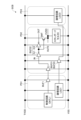
- First Embodiment Fig. 1 shows an example of a layout of a semiconductor device according to the first embodiment.
- the semiconductor device 100 shown in Fig. 1 may be a SoC (System on Chip), a standalone FPGA (Field-Programmable Gate Array), or the like.
- the semiconductor device 100 has a plurality of I/O cells IOC, IOCP and an internal circuit region INTR.
- the I/O cell IOC is an interface circuit for a signal SGNL such as an input signal, an output signal, or an input/output signal.
- the I/O cell IOCP is an interface circuit for a power supply potential or a ground potential.
- Each I/O cell IOC, IOCP is connected to an internal circuit region INTR.
- the internal circuit region INTR has one or more standard cell blocks SCB in which standard cells are provided.
- the internal circuit region INTR may also be equipped with logic circuits other than standard cells, or with memory.
- the memory may be equipped within the standard cell block SCB.
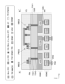
- FIG. 2 shows an example of a cross-sectional structure of the semiconductor device 100 of FIG. 1.
- the semiconductor device 100 has a substrate SUB, a wiring layer WL1 formed on the front surface FS side of the substrate SUB, and a wiring layer WL2 formed on the back surface BS side of the substrate SUB.
- the front surface FS of the substrate SUB is an example of the upper surface of the substrate SUB or the upper side of the substrate SUB
- the back surface BS of the substrate SUB is an example of the lower side of the substrate SUB.
- a fin FIN which is a part of a transistor, is formed on the front surface of the substrate SUB.
- the fin FIN has a source, drain, and channel.
- a pad PAD which is an external connection terminal, is formed on the surface (back surface) of the wiring layer WL2 opposite the substrate SUB.
- the wiring layer WL2 has multiple wiring layers BSM1 and BSM2 (two layers in FIG. 2, BSM stands for Backside Metal).
- BSM1 and BSM2 are formed with wiring W1 and W2, respectively, which supply power supply potential and ground potential, etc.
- the wiring W1 and W2 are connected to each other through a via VIA1.
- the wiring W2 and the pad PAD are connected to each other through a via VIA2.
- the wiring W1 is connected to the source and drain of the fin FIN via a TSV (Through Silicon Via) formed in the substrate SUB.
- the wiring W1 may be connected to a buried wiring BPR (Buried Power Rail) buried in the surface of the substrate SUB via the TSV.
- BPR Buried Power Rail
- the TSV is an example of a via.
- the transistors formed on the substrate SUB are not limited to fin FETs (Field Effect Transistors) using fins.
- the transistors formed on the substrate SUB may be planar MOSFETs (Metal Oxide Semiconductor FETs), nanosheet FETs, or CFETs (Complementary FETs).
- the TSVs that supply the power supply potential or ground potential are also connected to the source and drain of the transistor.
- the TSVs that supply the power supply potential or ground potential may be connected to the source and drain that are located closest to the substrate SUB.
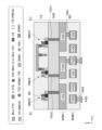
- FIG. 3 shows an example of a circuit arranged in the standard cell block SCB of FIG. 1.
- the standard cell block SCB has power domains PD1, PD2, and PD3 to which a power supply potential TVD and a ground potential VSS are supplied.
- the power supply potential TVD is an example of a second potential
- the power supply line TVD is an example of a second power supply line.
- the ground potential VSS is an example of a first potential
- the ground line VSS is an example of a first power supply line.
- the power domain PD1 has a control circuit CNTL1, a logic circuit LGC1, and a buffer BUF1 that operate on a power supply potential TVDD and a ground potential VSS.
- the power domain PD2 has buffers BUF21, BUF22, and BUF23, and a switch transistor SWT that operate on a power supply potential TVDD and a ground potential VSS that are constantly supplied.
- the power domain PD2 also has a standard cell SC that operates on a virtual power supply potential VVDD and a ground potential VSS.
- the power domain PD3 has a logic circuit LGC3 that operates by receiving a power supply potential TVDD and a ground potential VSS.
- the virtual power supply potential VVDD is an example of a third potential
- the virtual power line VVDD is an example of a third power supply line.
- Buffer BUF21 receives a control signal output from control circuit CNTL1 of power domain PD1 via buffer BUF1, and outputs it as an input signal IN to buffer BUF22.
- Buffer BUF22 has inverters IV1 and IV2 connected in series.
- Inverter IV1 receives the input signal IN and outputs an output signal OUT0 to inverter IV2 and the gate of switch transistor SWT.
- Inverter IV2 receives the output signal OUT0 and outputs an output signal OUT.
- the switch transistor SWT is a PMOS transistor with a source connected to the power supply line TVDD and a drain connected to the virtual power supply line VVDD, and operates by receiving the voltage of the output signal OUT0 output from the inverter IV1 as a gate potential. That is, the on/off of the switch transistor SWT is controlled by the control circuit CNTL1, and the supply or stop of the virtual power supply potential VVDD is switched by turning the switch transistor SWT on/off.
- the buffers BUF21 and BUF22 arranged in the power domain PD2 operate even when the switch transistor SWT is off and is not supplied with the virtual power potential VVDD. Therefore, in the power domain PD2 having the standard cell SC that operates at the virtual power potential VVDD, the on/off of the switch transistor SWT can be controlled by the control signal output from the control circuit CNTL1 of the power domain PD1.
- the standard cell SC has various logic circuits, such as, for example, a NAND circuit and an inverter.
- the standard cell SC may have an SRAM (Static Random Access Memory) or various macros.
- the buffer BUF23 receives a signal output from the logic circuit LGC1 of the power domain PD1, and outputs the received signal to the logic circuit LGC3 of the power domain PD3.
- the buffer BUF23 arranged in the power domain PD2 operates even when the switch transistor SWT is off and the virtual power supply potential VVDD is not supplied. Therefore, in the power domain PD2 having the standard cell SC that operates at the virtual power supply potential VVDD, the signal output from the logic circuit LGC1 of the power domain PD1 can be transmitted to the power domain PD3 via the BUF23 of the power domain PD2.
- the buffers BUF21, BUF22, and BUF23 that are capable of operating at all times and are arranged in the power domain PD2, which can supply and stop the virtual power potential VVDD, are sometimes called AOBs (Always on Buffers).
- the AOBs may be designed as cells.
- the AOBs are used to transmit control signals that control circuits such as the switch transistor SWT in the power domain PD2, or to transmit signals (signals not used in the power domain PD2) between other power domains such as the power domains PD1 and PD3.
- the AOBs are an example of a first circuit.
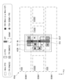
- FIG. 4 shows an example of the positional relationship between the power lines and vias arranged in the power domain PD2 of FIG. 3 in a plan view on the back side of the semiconductor substrate SUB, and the AOB.
- each wire in the wiring layer BSM1 extends in the X direction
- each wire in the wiring layer BSM2 extends in the Y direction that is different from the X direction.
- the X direction is an example of the first direction
- the Y direction is an example of the second direction.
- the symbol ROW in FIG. 4 indicates the width of the standard cell SC in the Y direction in the wiring layer BSM1.
- the virtual power lines VVDD of the wiring layer BSM1 are arranged in the Y direction at a pitch twice that of the ROW. Between a pair of virtual power lines VVDD adjacent in the Y direction, ground lines VSS extending in the X direction and interrupted at multiple points along the way, and power lines TVDD arranged at positions where the ground lines VSS are interrupted, are arranged alternately along the X direction. In other words, the power lines TVDD are arranged between multiple ground lines VSS in the X direction.
- the AOBs shown in thick dashed lines are arranged, for example, in a staggered pattern (zigzag) at positions that overlap with parts of the power supply lines TVDD and ground lines VSS in a plan view.
- standard cells SC (not shown) are arranged.
- the power supply line TVD can be arranged only in positions where the AOBs are arranged. This allows the arrangement density of the virtual power supply lines VVDD and the ground lines VSS in the wiring layer BSM1 to be increased compared to the case where a dedicated area is provided for the power supply line TVD that is wired with an interval ROW, and the power supply capacity to the standard cells SC can be increased.
- the power supply line TVD, the virtual power supply line VVDD, and the ground line VSS are repeatedly arranged in the X direction.
- the virtual power supply lines VVDD of the wiring layers BSM1 and BSM2 are connected to each other through vias VIA1 arranged at the intersections.
- the power supply lines TVD of the wiring layers BSM1 and BSM2 are connected to each other through vias VIA1 arranged at the intersections.
- the ground lines VSS of the wiring layers BSM1 and BSM2 are connected to each other through vias VIA1 arranged at the intersections.
- the virtual power line VVDD may be omitted from the wiring layer BSM2.
- the power line TVDD and the ground line VSS may be arranged alternately along the X direction in the wiring layer BSM2.
- the placement density of the AOBs is set according to the required number of AOBs to be placed in the power domain PD2.
- the cut interval of the ground lines VSS extending in the X direction in the wiring layer BSM1 may be changed, and the placement interval of the power lines TVDD in the Y direction in the wiring layer BSM1 may be changed.
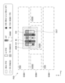
- FIG. 5 shows an example of the layout of AOB in FIG. 4.
- AOB in FIG. 5 shows buffer BUF22 in FIG. 3, but may also be buffer BUF21 or buffer BUF23 in FIG. 3.
- symbol LI indicates local wiring formed on substrate SUB.
- Wiring LI can be directly connected to the source and drain of a transistor.
- Symbol Mint indicates wiring formed in metal wiring layer Mint, which is a wiring layer on wiring LI.
- Symbol GT indicates the gate of a transistor.
- Symbol VIA indicates a via that connects Mint wiring and local wiring LI, or a via that connects Mint wiring and gate GT.
- TR(PMOS) indicates the transistor region (source, drain, and channel) of a PMOS transistor.
- TR(NMOS) indicates the transistor region (source, drain, and channel) of an NMOS transistor.
- a PMOS transistor is an example of a second transistor, and an NMOS transistor is an example of a first transistor.
- a fin is formed in the region TR.
- a semiconductor layer is formed as the source and drain in the region TR, and a nanosheet is formed as the channel between the source and drain.
- AOB is arranged in a position in the wiring layer BSM1 where it overlaps with part of the power supply line TVDD and part of the ground line VSS in a planar view.
- the NMOS transistors of inverters IV1 and IV2 included in AOB are arranged in a position where it overlaps with the ground line VSS of the wiring layer BSM1 in a planar view.
- the PMOS transistors of inverters IV1 and IV2 included in AOB are arranged in a position where it overlaps with the power supply line TVDD of the wiring layer BSM1 in a planar view.
- the sources of the NMOS transistors of inverters IV1 and IV2 are directly connected to the ground line VSS of wiring layer BSM1 via TSV.
- the sources of the PMOS transistors of inverters IV1 and IV2 are directly connected to the power supply line TVDD of wiring layer BSM1 via TSV. This allows the power supply potential TVDD and the ground potential VSS to be directly supplied to the sources of the transistors of the AOB from the back side of the substrate SUB ( Figure 2), making it possible to reduce the layout size of the AOB and arrange the AOB efficiently.
- direct connection means that the conductors contained in the TSV are in contact with the source, drain, etc. of each transistor.
- the TSV has multiple layers of conductors, it also includes cases where some of the multiple layers of conductors are in contact with the source or drain of the transistor.
- each of the power supply line TVD and ground line VSS of the wiring layer BSM1 is connected to a corresponding power supply line TVD and ground line VSS in the wiring layer BSM2 (not shown).
- the virtual power supply line VVDD of the wiring layer BSM1 may be connected to the virtual power supply line VVDD of the wiring layer BSM2.
- FIG. 6 shows an example of a cross section along line X1-X1' in FIG. 5.
- the ground line VSS formed in the wiring layer BSM1 on the back surface BS side of the substrate SUB is connected to the source S (N-type impurity region) of the NMOS transistor formed on the front surface FS of the substrate SUB via a TSV1 formed in the substrate SUB.
- the power supply line TVDD formed in the wiring layer BSM1 on the back surface BS side is connected to the source S (P-type impurity region) of the PMOS transistor formed on the front surface FS via a TSV2 formed in the substrate SUB.
- each fin FIN a channel C is arranged between a source S and a drain D.
- a gate GT is arranged on the channel C via a gate insulating film (not shown).
- two wiring layers BSM1 and BSM2 are arranged on the back surface BS side, but three or more wiring layers BSM may be arranged.
- FIG. 7 shows another example of a cross section taken along line X1-X1' in FIG. 5. Elements and layouts that are the same as or similar to those in FIG. 6 are indicated with the same symbols or the same patterns, and detailed explanations are omitted.
- FIG. 7 has the same cross-sectional structure as FIG. 6, except that the position where the wiring of the wiring layer BSM1 is formed is different.
- the wiring of the wiring layer BSM1 is formed below the substrate SUB, on the back surface BS side of the substrate SUB.
- FIG. 8 shows another example of a cross section along line X1-X1' in FIG. 5. Elements and layouts that are the same as or similar to those in FIG. 6 are indicated with the same symbols or the same patterns, and detailed descriptions are omitted.
- FIG. 8 has the same cross-sectional structure as FIG. 6, except that the position where the wiring of the wiring layer BSM1 is formed is different. The wiring of the wiring layer BSM1 is not exposed on the back surface BS side of the substrate SUB, but is formed inside the substrate SUB.
- the wiring of the wiring layer BSM1 formed in the substrate SUB is connected to the wiring of the wiring layer BSM2 through a via VIA1 formed in the substrate SUB, and is connected to the source S of the fin FIN through a via VIA3 formed in the substrate SUB.
- FIG. 9 shows yet another example of a cross section taken along line X1-X1' in FIG. 5. Elements and layouts that are the same as or similar to those in FIG. 6 are indicated with the same symbols or the same patterns, and detailed descriptions are omitted.
- FIG. 9 has the same cross-sectional structure as FIG. 6, except that the transistor formed on the substrate SUB is a nanosheet FET.
- the nanosheet FET has a semiconductor layer having a source S and a drain D, a nanosheet NS having a semiconductor material formed between the source S and the drain D, and a gate GT formed via a gate insulating film (not shown) provided on the surface of the nanosheet NS. Note that a nanosheet FET may be arranged in place of the finFET shown in FIG. 6, FIG. 7, or FIG. 8.
- FIG. 10 shows a modified layout of the AOB in FIG. 4. Elements and layouts that are the same as or similar to those in FIG. 5 are indicated with the same symbols or the same patterns, and detailed descriptions are omitted.
- the layout in FIG. 10 is similar to the layout in FIG. 5, except that an N-type well tap NWTP and a P-type well tap PWTP are arranged in regions adjacent to both sides of the AOB in the X direction.
- NWTP is an example of a first well tap
- the well tap NWTP is an example of a second well tap.
- the well tap PWTP is disposed at a position overlapping the ground line VSS of the wiring layer BSM1 in a plan view.
- the well tap PWTP is formed by a PMOS transistor whose source and drain are directly connected to the ground line VSS of the wiring layer BSM1 via a TSV. This allows the ground potential VSS to be supplied to the P-type well region PW, which is the substrate region (region other than the shaded region) of the NMOS transistor.
- the well tap NWTP is placed at a position overlapping the power supply line TVDD of the wiring layer BSM1 in a plan view.
- the well tap NWTP is formed by an NMOS transistor whose source and drain are directly connected to the power supply line TVDD of the wiring layer BSM1 via a TSV. This makes it possible to supply the power supply potential TVDD to the N-type well region NW, which is the substrate region (shaded region) of the PMOS transistor.
- the design efficiency of the circuit region can be improved.
- the sources of the NMOS transistor and PMOS transistor of the AOB are directly connected to the ground line VSS and power line TVDD of the wiring layer BSM1 via the TSV. This makes it possible to directly supply the power supply potential TVDD and the ground potential VSS to the AOB from the back side of the substrate SUB, thereby reducing the layout size of the AOB and enabling the AOB to be arranged efficiently.
- the power supply line TVD can be arranged only in positions where the AOBs are arranged. This allows the arrangement density of the virtual power supply lines VVDD and the ground line VSS in the wiring layer BSM1 to be increased compared to the case where the power supply line TVD extending in the X direction together with the virtual power supply line VVDD and the ground line VSS is arranged in the semi-circular BSM1, and the power supply capacity to the standard cells SC can be increased.
- the well tap PWTP By arranging the well tap PWTP at a position overlapping with the ground line VSS of the wiring layer BSM1 in a plan view, it is possible to supply the ground potential VSS to the P-type well region PW in which the substrate region of the NMOS transistor is located.
- the well tap NWTP By arranging the well tap NWTP at a position overlapping with the power supply line TVDD of the wiring layer BSM1 in a plan view, it is possible to supply the power supply potential TVDD to the N-type well region NW in which the substrate region of the PMOS transistor is located.
- Second Embodiment 11 shows an example of the layout of the AOB in the semiconductor device of the second embodiment.
- the same or similar elements and layout as those in FIG. 5 are indicated by the same symbols or the same patterns, and detailed description is omitted.
- the power domain PD2 shown in FIG. 11 is provided in the standard cell block SCB of FIG. 1 together with the power domains PD1 and PD3 as shown in FIG. 3.
- the ground lines VSS of the wiring layer BSM1 are formed to extend in the X direction. Between a pair of ground lines VSS adjacent to each other in the Y direction, virtual power lines VVDD extending in the X direction and interrupted at multiple points along the way, and power lines TVDD arranged at positions where the virtual power lines VVDD are interrupted are arranged alternately along the X direction. Note that the AOBs are arranged alternately (staggered) within the power domain PD2, as in FIG. 4.
- the inverters IV1 and IV2 of the AOB are arranged side by side in the Y direction.
- the NMOS transistors of the inverters IV1 and IV2 are arranged in a position overlapping the ground line VSS of the wiring layer BSM1 in a planar view.
- the PMOS transistors of the inverters IV1 and IV2 are arranged in a position overlapping the power supply line TVD of the wiring layer BSM1 in a planar view.
- FIG. 12 shows a modified layout of the AOB in FIG. 11. Elements and layouts that are the same as or similar to those in FIG. 11 are indicated with the same symbols or the same patterns, and detailed descriptions are omitted.
- the AOB is arranged across the boundary between the power supply line TVDD and the ground line VSS in the wiring layer BSM1, and the inverters IV1 and IV2 are arranged side by side in the X direction.
- the NMOS transistors of the inverters IV1 and IV2 are arranged in a position that overlaps with the ground line VSS of the wiring layer BSM1 in a plan view.
- the PMOS transistors of the inverters IV1 and IV2 are arranged in a position that overlaps with the power supply line TVDD of the wiring layer BSM1 in a plan view.
- the sources of the PMOS transistors of the inverters IV1 and IV2 are common and connected to the power supply line TVDD of the wiring layer BSM1 via a common TSV.
- the sources of the NMOS transistors of the inverters IV1 and IV2 are common and connected to the ground line VSS of the wiring layer BSM1 via a common TSV.
- the source of the PMOS transistor can be directly connected to the power supply line TVDD of the wiring layer BSM1 via the TSV, and the source of the NMOS transistor can be directly connected to the ground line VSS of the wiring layer BSM1 via the TSV. Furthermore, by sharing the TSV, it becomes possible to make the layout size of the AOB smaller than those of FIG. 5 and FIG. 11.
- the sources of the PMOS transistors of the inverters IV1 and IV2 may be provided independently of each other, and the sources of the NMOS transistors of the inverters IV1 and IV2 may be provided independently of each other. In other embodiments and modifications, the sources of the PMOS transistors of the inverters IV1 and IV2 may be shared, and the sources of the NMOS transistors of the inverters IV1 and IV2 may be shared.
- the second embodiment can also achieve the same effects as the first embodiment.
- the power supply potential TVDD and the ground potential VSS can be directly supplied to the AOB from the back side of the substrate SUB, and the layout size of the AOB can be reduced and the AOB can be efficiently arranged.
- the power supply line TVDD is arranged at a position where the virtual power supply line VVDD extending in the X direction is interrupted, the power supply potential TVDD and the ground potential VSS can be directly supplied to the AOB from the back side of the substrate SUB.
- the sources of the PMOS transistors of the inverters IV1 and IV2 are common and connected to the power supply line TVDD of the wiring layer BSM1 via a common TSV.
- the sources of the NMOS transistors of the inverters IV1 and IV2 are common and connected to the ground line VSS of the wiring layer BSM1 via a common TSV. This allows the layout size of the AOB to be further reduced, and the AOB to be arranged more efficiently.
- Third Embodiment 13 shows an example of the positional relationship between the AOB and the power supply lines and vias arranged at positions overlapping the standard cell blocks in FIG. 3 in a plan view in the semiconductor device of the third embodiment. Elements and layouts that are the same as or similar to those in FIG. 4 are indicated by the same symbols or patterns, and detailed descriptions thereof will be omitted.
- the power domain PD2 shown in FIG. 13 is provided in the standard cell block SCB in FIG. 1 together with the power domains PD1 and PD3 as shown in FIG. 3.
- the power wiring in the wiring layer BSM1 is not interrupted, and the ground line VSS, power line TVDD, and virtual power line VVDD extending in the X direction are arranged side by side in the Y direction.
- the AOB is arranged at a position overlapping the ground line VSS and power line TVDD adjacent to each other in the wiring layer BSM1.
- FIG. 14 shows an example of the layout of the AOB in FIG. 13. Elements and layouts that are the same as or similar to those in FIG. 5 are indicated with the same symbols or the same patterns, and detailed descriptions are omitted.
- the layout of the AOB shown in FIG. 4 is the same as or similar to the layout of the AOB in FIG. 12. That is, the AOB is arranged across the boundary between the power supply line TVDD and the ground line VSS in the wiring layer BSM1, and the inverters IV1 and IV2 are arranged side by side in the X direction.
- the sources of the PMOS transistors of the inverters IV1 and IV2 are common and connected to the power supply line TVDD of the wiring layer BSM1 via a common TSV.
- the sources of the NMOS transistors of the inverters IV1 and IV2 are common and connected to the ground line VSS of the wiring layer BSM1 via a common TSV.
- the sources of the PMOS transistors of the inverters IV1 and IV2 may be provided independently of each other. Also, the sources of the NMOS transistors of the inverters IV1 and IV2 may be provided independently of each other.
- the third embodiment can achieve the same effects as the first embodiment.
- the power supply potential TVDD and the ground potential VSS can be directly supplied to the AOB from the back surface side of the substrate SUB, and the layout size of the AOB can be reduced and the AOB can be arranged efficiently.
- the layout size of the AOB can be reduced and the AOB can be arranged efficiently.
- FIG. 15 shows an example of the layout of the AOB in the semiconductor device of the fourth embodiment.
- the same or similar elements and layout as those in Fig. 5 are indicated by the same symbols or the same patterns, and detailed description is omitted.
- the power domain PD2 shown in Fig. 15 is provided in the standard cell block SCB of Fig. 1 together with the power domains PD1 and PD3 as shown in Fig. 3.
- the layout of the ground line VSS, virtual power line VVDD, and power line TVDD of the wiring layer BSM1 in FIG. 15 is the same as that in FIG. 11. That is, the ground line VSS is formed extending in the X direction. Between a pair of ground lines VSS adjacent to each other in the Y direction, a virtual power line VVDD that extends in the X direction and is interrupted at multiple points along the way, and a power line TVDD that is arranged at the position where the virtual power line VVDD is interrupted are arranged alternately along the X direction.
- the power tap cell TPC is placed at a position overlapping the virtual power line VVDD of the wiring layer BSM1 in a planar view.
- two AOB1 and AOB2 are placed side by side in the X direction at positions overlapping the power line TVDD and the ground line VSS of the wiring layer BSM1 in a planar view.
- the power tap cell TPC has a PMOS transistor whose source and drain are directly connected to the power line TVDD of the wiring layer BSM1 via a TSV.
- the power tap cell TPC also has a PMOS transistor whose source and drain are directly connected to the ground line VSS of the wiring layer BSM1 via a TSV.
- the source and drain of a transistor are an example of a semiconductor layer.
- the inverters IV1 and IV2 of each of AOB1 and AOB2 are arranged side by side in the Y direction, as in FIG. 11.
- the PMOS transistors of the inverters IV1 and IV2 are arranged in a position overlapping the power line TVDD of the wiring layer BSM1 in a plan view.
- the sources of the PMOS transistors of each of AOB1 and AOB2 are connected to the source and drain of the PMOS transistor of the power tap cell TPC via the Mint wiring extending in the Y direction, the via VIA, and the local wiring LI extending in the X direction. That is, each of AOB1 and AOB2 receives the power supply potential TVDD supplied from the power tap cell TPC.
- the NMOS transistors of inverters IV1 and IV2 are arranged in a position overlapping the ground line VSS of wiring layer BSM1 in a plan view, and the sources of the NMOS transistors are directly connected to the ground line VSS of wiring layer BSM1 via TSVs.
- a power tap cell TPC is arranged at a position corresponding to the power line TVDD of the wiring layer BSM1, and the power tap cell TPC supplies a power supply potential TVDD to multiple AOB1 and AOB2.
- AOC to be placed not only in a position opposite the power line TVDD of the wiring layer BSM1, but also in a position opposite the virtual power line VVDD of the wiring layer BSM1.
- the number of power lines TVDD of the wiring layer BSM1 can be reduced, and the area occupied by free space in the circuit area can be reduced. This makes it possible to suppress an increase in the element area.
- the power line TVDD of the wiring layer BSM1 is placed in a position corresponding to each of AOB1 and AOB2, free space is required for the power line TVDD corresponding to each of AOB1 and AOB2, which may increase the element area.
- the fourth embodiment can also achieve the same effects as the first embodiment.
- the power supply potential TVDD and the ground potential VSS can be directly supplied to the AOB from the back side of the substrate SUB, and the layout size of the AOB can be reduced, allowing the AOB to be arranged efficiently.
- the power tap cell TPC arranged at a position overlapping the power line TVDD of the wiring layer BSM1 in a plan view is connected to the sources of the PMOS transistors of the multiple AOBs via wiring.
- This allows the number of power lines TVDD of the wiring layer BSM1 to be reduced compared to the case where the power line TVDD of the wiring layer BSM1 is arranged for each AOB, and the area occupied by free space in the circuit area can be reduced.
- the power line TVDD of the wiring layer BSM1 is arranged at a position where the virtual power line VVDD is interrupted, but even if the power line TVDD is arranged at a position where the ground line VSS of the wiring layer BSM1 is interrupted, the power tap cell TPC may supply the power potential TVDD to the multiple AOB1 and AOB2. Also, a similar configuration may be used in other embodiments.
- FIG. 16 shows an example of a circuit arranged in a standard cell block SCB in a semiconductor device according to the fifth embodiment. Elements that are the same as or similar to those in Fig. 3 are given the same reference numerals, and detailed description thereof will be omitted.
- the standard cell block SCB shown in Fig. 16 is mounted in the internal circuit region INTR of the semiconductor device 100, similar to that in Fig. 1.
- the standard cell block SCB shown in FIG. 16 has power domains PD1 and PD3 to which a power supply potential TVDD and a ground potential are supplied, and a power domain PD2 to which a power supply potential VVDD and a ground potential VSS are supplied, similar to FIG. 3.
- the power domains PD1 and PD3 are the same as the power domains PD1 and PD3 in FIG. 3, respectively.
- the power domain PD2 does not have the switch transistor SWT included in the power domain PD2 of FIG. 3.
- a virtual power supply potential VVDD supplied from a power supply management IC (Integrated Circuit) provided outside the semiconductor device 100 is supplied to a virtual power supply line VVDD in the power domain PD2 via a switch SW.
- the power supply management IC may be disposed on the board on which the semiconductor device 100 is mounted, or may be disposed outside the board on which the semiconductor device 100 is mounted.
- the buffer BUF22 is used to control the circuit of the power domain PD2 or the circuit of the power domain PD3.
- the layout and cross-sectional structure of the AOBs such as the buffers BUF21, BUF22, and BUF23 are the same as or similar to the layout and cross-sectional structure of the AOBs in the first to fourth embodiments.
- the fifth embodiment can also achieve the same effects as the first to fourth embodiments.
Landscapes
- Engineering & Computer Science (AREA)
- Power Engineering (AREA)
- Design And Manufacture Of Integrated Circuits (AREA)
- Semiconductor Integrated Circuits (AREA)
Priority Applications (4)
| Application Number | Priority Date | Filing Date | Title |
|---|---|---|---|
| PCT/JP2023/021508 WO2024252660A1 (ja) | 2023-06-09 | 2023-06-09 | 半導体装置 |
| JP2025525905A JPWO2024252660A1 (https=) | 2023-06-09 | 2023-06-09 | |
| CN202380099236.2A CN121312285A (zh) | 2023-06-09 | 2023-06-09 | 半导体装置 |
| US19/412,052 US20260096419A1 (en) | 2023-06-09 | 2025-12-08 | Semiconductor device |
Applications Claiming Priority (1)
| Application Number | Priority Date | Filing Date | Title |
|---|---|---|---|
| PCT/JP2023/021508 WO2024252660A1 (ja) | 2023-06-09 | 2023-06-09 | 半導体装置 |
Related Child Applications (1)
| Application Number | Title | Priority Date | Filing Date |
|---|---|---|---|
| US19/412,052 Continuation US20260096419A1 (en) | 2023-06-09 | 2025-12-08 | Semiconductor device |
Publications (1)
| Publication Number | Publication Date |
|---|---|
| WO2024252660A1 true WO2024252660A1 (ja) | 2024-12-12 |
Family
ID=93795559
Family Applications (1)
| Application Number | Title | Priority Date | Filing Date |
|---|---|---|---|
| PCT/JP2023/021508 Ceased WO2024252660A1 (ja) | 2023-06-09 | 2023-06-09 | 半導体装置 |
Country Status (4)
| Country | Link |
|---|---|
| US (1) | US20260096419A1 (https=) |
| JP (1) | JPWO2024252660A1 (https=) |
| CN (1) | CN121312285A (https=) |
| WO (1) | WO2024252660A1 (https=) |
Citations (5)
| Publication number | Priority date | Publication date | Assignee | Title |
|---|---|---|---|---|
| WO2021070367A1 (ja) * | 2019-10-11 | 2021-04-15 | 株式会社ソシオネクスト | 半導体装置 |
| WO2021070366A1 (ja) * | 2019-10-11 | 2021-04-15 | 株式会社ソシオネクスト | 半導体装置 |
| WO2021079511A1 (ja) * | 2019-10-25 | 2021-04-29 | 株式会社ソシオネクスト | 半導体装置 |
| WO2021111604A1 (ja) * | 2019-12-05 | 2021-06-10 | 株式会社ソシオネクスト | 半導体装置 |
| WO2023054602A1 (ja) * | 2021-09-30 | 2023-04-06 | 株式会社ソシオネクスト | 半導体装置 |
-
2023
- 2023-06-09 JP JP2025525905A patent/JPWO2024252660A1/ja active Pending
- 2023-06-09 WO PCT/JP2023/021508 patent/WO2024252660A1/ja not_active Ceased
- 2023-06-09 CN CN202380099236.2A patent/CN121312285A/zh active Pending
-
2025
- 2025-12-08 US US19/412,052 patent/US20260096419A1/en active Pending
Patent Citations (5)
| Publication number | Priority date | Publication date | Assignee | Title |
|---|---|---|---|---|
| WO2021070367A1 (ja) * | 2019-10-11 | 2021-04-15 | 株式会社ソシオネクスト | 半導体装置 |
| WO2021070366A1 (ja) * | 2019-10-11 | 2021-04-15 | 株式会社ソシオネクスト | 半導体装置 |
| WO2021079511A1 (ja) * | 2019-10-25 | 2021-04-29 | 株式会社ソシオネクスト | 半導体装置 |
| WO2021111604A1 (ja) * | 2019-12-05 | 2021-06-10 | 株式会社ソシオネクスト | 半導体装置 |
| WO2023054602A1 (ja) * | 2021-09-30 | 2023-04-06 | 株式会社ソシオネクスト | 半導体装置 |
Also Published As
| Publication number | Publication date |
|---|---|
| US20260096419A1 (en) | 2026-04-02 |
| JPWO2024252660A1 (https=) | 2024-12-12 |
| CN121312285A (zh) | 2026-01-09 |
Similar Documents
| Publication | Publication Date | Title |
|---|---|---|
| US12310103B2 (en) | Semiconductor integrated circuit device having standard cells including three dimensional transistors | |
| US12094882B2 (en) | Semiconductor integrated circuit device | |
| CN112753098A (zh) | 半导体装置 | |
| JP7529121B2 (ja) | 半導体装置 | |
| JP7639871B2 (ja) | 半導体装置 | |
| WO2023054602A1 (ja) | 半導体装置 | |
| JP7736152B2 (ja) | 半導体装置 | |
| US12211851B2 (en) | Semiconductor device including standard cells | |
| WO2023054601A1 (ja) | 半導体装置 | |
| TWI866118B (zh) | 半導體裝置和準位位移電路 | |
| WO2024252660A1 (ja) | 半導体装置 | |
| US20260033000A1 (en) | Semiconductor device | |
| JP2000223575A (ja) | 半導体装置の設計方法、半導体装置および半導体装置の製造方法 | |
| US20260040683A1 (en) | Semiconductor device | |
| WO2023132264A1 (ja) | 半導体集積回路装置 | |
| US20260107756A1 (en) | Semiconductor device | |
| JP7848630B2 (ja) | 半導体装置 | |
| JP5029272B2 (ja) | 半導体集積回路 | |
| WO2025181960A1 (ja) | 半導体装置 | |
| WO2025169464A1 (ja) | 半導体装置 | |
| WO2025181961A1 (ja) | 半導体装置 | |
| WO2025079229A1 (ja) | 半導体装置 | |
| WO2025079230A1 (ja) | 半導体装置 | |
| WO2025083833A1 (ja) | 半導体装置 | |
| WO2025079232A1 (ja) | 半導体装置 |
Legal Events
| Date | Code | Title | Description |
|---|---|---|---|
| 121 | Ep: the epo has been informed by wipo that ep was designated in this application |
Ref document number: 23940758 Country of ref document: EP Kind code of ref document: A1 |
|
| ENP | Entry into the national phase |
Ref document number: 2025525905 Country of ref document: JP Kind code of ref document: A |
|
| WWE | Wipo information: entry into national phase |
Ref document number: 2025525905 Country of ref document: JP |
|
| NENP | Non-entry into the national phase |
Ref country code: DE |