WO2024252613A1 - 静電チャックおよびサセプタ - Google Patents
静電チャックおよびサセプタ Download PDFInfo
- Publication number
- WO2024252613A1 WO2024252613A1 PCT/JP2023/021338 JP2023021338W WO2024252613A1 WO 2024252613 A1 WO2024252613 A1 WO 2024252613A1 JP 2023021338 W JP2023021338 W JP 2023021338W WO 2024252613 A1 WO2024252613 A1 WO 2024252613A1
- Authority
- WO
- WIPO (PCT)
- Prior art keywords
- electrostatic chuck
- flat
- wafer
- inclined portion
- thickness direction
- Prior art date
- Legal status (The legal status is an assumption and is not a legal conclusion. Google has not performed a legal analysis and makes no representation as to the accuracy of the status listed.)
- Ceased
Links
Images


Classifications
-
- H—ELECTRICITY
- H10—SEMICONDUCTOR DEVICES; ELECTRIC SOLID-STATE DEVICES NOT OTHERWISE PROVIDED FOR
- H10P—GENERIC PROCESSES OR APPARATUS FOR THE MANUFACTURE OR TREATMENT OF DEVICES COVERED BY CLASS H10
- H10P72/00—Handling or holding of wafers, substrates or devices during manufacture or treatment thereof
- H10P72/70—Handling or holding of wafers, substrates or devices during manufacture or treatment thereof for supporting or gripping
- H10P72/72—Handling or holding of wafers, substrates or devices during manufacture or treatment thereof for supporting or gripping using electrostatic chucks
- H10P72/722—Details of electrostatic chucks
-
- H—ELECTRICITY
- H02—GENERATION; CONVERSION OR DISTRIBUTION OF ELECTRIC POWER
- H02N—ELECTRIC MACHINES NOT OTHERWISE PROVIDED FOR
- H02N13/00—Clutches or holding devices using electrostatic attraction, e.g. using Johnson-Rahbek effect
-
- H—ELECTRICITY
- H05—ELECTRIC TECHNIQUES NOT OTHERWISE PROVIDED FOR
- H05B—ELECTRIC HEATING; ELECTRIC LIGHT SOURCES NOT OTHERWISE PROVIDED FOR; CIRCUIT ARRANGEMENTS FOR ELECTRIC LIGHT SOURCES, IN GENERAL
- H05B3/00—Ohmic-resistance heating
- H05B3/10—Heating elements characterised by the composition or nature of the materials or by the arrangement of the conductor
- H05B3/12—Heating elements characterised by the composition or nature of the materials or by the arrangement of the conductor characterised by the composition or nature of the conductive material
- H05B3/14—Heating elements characterised by the composition or nature of the materials or by the arrangement of the conductor characterised by the composition or nature of the conductive material the material being non-metallic
- H05B3/141—Conductive ceramics, e.g. metal oxides, metal carbides, barium titanate, ferrites, zirconia, vitrous compounds
- H05B3/143—Conductive ceramics, e.g. metal oxides, metal carbides, barium titanate, ferrites, zirconia, vitrous compounds applied to semiconductors, e.g. wafers heating
-
- H—ELECTRICITY
- H05—ELECTRIC TECHNIQUES NOT OTHERWISE PROVIDED FOR
- H05B—ELECTRIC HEATING; ELECTRIC LIGHT SOURCES NOT OTHERWISE PROVIDED FOR; CIRCUIT ARRANGEMENTS FOR ELECTRIC LIGHT SOURCES, IN GENERAL
- H05B6/00—Heating by electric, magnetic or electromagnetic fields
- H05B6/02—Induction heating
- H05B6/10—Induction heating apparatus, other than furnaces, for specific applications
- H05B6/105—Induction heating apparatus, other than furnaces, for specific applications using a susceptor
-
- H—ELECTRICITY
- H10—SEMICONDUCTOR DEVICES; ELECTRIC SOLID-STATE DEVICES NOT OTHERWISE PROVIDED FOR
- H10P—GENERIC PROCESSES OR APPARATUS FOR THE MANUFACTURE OR TREATMENT OF DEVICES COVERED BY CLASS H10
- H10P72/00—Handling or holding of wafers, substrates or devices during manufacture or treatment thereof
- H10P72/04—Apparatus for manufacture or treatment
- H10P72/0402—Apparatus for fluid treatment
-
- H—ELECTRICITY
- H10—SEMICONDUCTOR DEVICES; ELECTRIC SOLID-STATE DEVICES NOT OTHERWISE PROVIDED FOR
- H10P—GENERIC PROCESSES OR APPARATUS FOR THE MANUFACTURE OR TREATMENT OF DEVICES COVERED BY CLASS H10
- H10P72/00—Handling or holding of wafers, substrates or devices during manufacture or treatment thereof
- H10P72/04—Apparatus for manufacture or treatment
- H10P72/0431—Apparatus for thermal treatment
- H10P72/0434—Apparatus for thermal treatment mainly by convection
-
- H—ELECTRICITY
- H10—SEMICONDUCTOR DEVICES; ELECTRIC SOLID-STATE DEVICES NOT OTHERWISE PROVIDED FOR
- H10P—GENERIC PROCESSES OR APPARATUS FOR THE MANUFACTURE OR TREATMENT OF DEVICES COVERED BY CLASS H10
- H10P72/00—Handling or holding of wafers, substrates or devices during manufacture or treatment thereof
- H10P72/70—Handling or holding of wafers, substrates or devices during manufacture or treatment thereof for supporting or gripping
- H10P72/72—Handling or holding of wafers, substrates or devices during manufacture or treatment thereof for supporting or gripping using electrostatic chucks
-
- H—ELECTRICITY
- H10—SEMICONDUCTOR DEVICES; ELECTRIC SOLID-STATE DEVICES NOT OTHERWISE PROVIDED FOR
- H10P—GENERIC PROCESSES OR APPARATUS FOR THE MANUFACTURE OR TREATMENT OF DEVICES COVERED BY CLASS H10
- H10P72/00—Handling or holding of wafers, substrates or devices during manufacture or treatment thereof
- H10P72/70—Handling or holding of wafers, substrates or devices during manufacture or treatment thereof for supporting or gripping
- H10P72/76—Handling or holding of wafers, substrates or devices during manufacture or treatment thereof for supporting or gripping using mechanical means, e.g. clamps or pinches
- H10P72/7604—Handling or holding of wafers, substrates or devices during manufacture or treatment thereof for supporting or gripping using mechanical means, e.g. clamps or pinches the wafers being placed on a susceptor, stage or support
- H10P72/7611—Handling or holding of wafers, substrates or devices during manufacture or treatment thereof for supporting or gripping using mechanical means, e.g. clamps or pinches the wafers being placed on a susceptor, stage or support characterised by edge profile or support profile
-
- H—ELECTRICITY
- H10—SEMICONDUCTOR DEVICES; ELECTRIC SOLID-STATE DEVICES NOT OTHERWISE PROVIDED FOR
- H10P—GENERIC PROCESSES OR APPARATUS FOR THE MANUFACTURE OR TREATMENT OF DEVICES COVERED BY CLASS H10
- H10P72/00—Handling or holding of wafers, substrates or devices during manufacture or treatment thereof
- H10P72/70—Handling or holding of wafers, substrates or devices during manufacture or treatment thereof for supporting or gripping
- H10P72/76—Handling or holding of wafers, substrates or devices during manufacture or treatment thereof for supporting or gripping using mechanical means, e.g. clamps or pinches
- H10P72/7604—Handling or holding of wafers, substrates or devices during manufacture or treatment thereof for supporting or gripping using mechanical means, e.g. clamps or pinches the wafers being placed on a susceptor, stage or support
- H10P72/7614—Handling or holding of wafers, substrates or devices during manufacture or treatment thereof for supporting or gripping using mechanical means, e.g. clamps or pinches the wafers being placed on a susceptor, stage or support characterised by a plurality of individual support members, e.g. support posts or protrusions
-
- H—ELECTRICITY
- H10—SEMICONDUCTOR DEVICES; ELECTRIC SOLID-STATE DEVICES NOT OTHERWISE PROVIDED FOR
- H10P—GENERIC PROCESSES OR APPARATUS FOR THE MANUFACTURE OR TREATMENT OF DEVICES COVERED BY CLASS H10
- H10P72/00—Handling or holding of wafers, substrates or devices during manufacture or treatment thereof
- H10P72/70—Handling or holding of wafers, substrates or devices during manufacture or treatment thereof for supporting or gripping
- H10P72/76—Handling or holding of wafers, substrates or devices during manufacture or treatment thereof for supporting or gripping using mechanical means, e.g. clamps or pinches
- H10P72/7604—Handling or holding of wafers, substrates or devices during manufacture or treatment thereof for supporting or gripping using mechanical means, e.g. clamps or pinches the wafers being placed on a susceptor, stage or support
- H10P72/7624—Handling or holding of wafers, substrates or devices during manufacture or treatment thereof for supporting or gripping using mechanical means, e.g. clamps or pinches the wafers being placed on a susceptor, stage or support characterised by the mechanical construction of the susceptor, stage or support
Definitions
- Electrostatic chucks that use electrostatic attraction to secure workpieces are widely used in etching devices such as plasma etching devices, and film-forming devices such as PVD devices, CVD devices, and ion plating devices used in semiconductor manufacturing processes.
- One such electrostatic chuck is already known in which the mounting surface on which a plate-shaped workpiece such as a semiconductor wafer is placed is an uneven surface with multiple convex portions (protrusions), the workpiece is supported by the convex portions, and a cooling gas can be flowed through the concave portions (see, for example, Patent Documents 1 and 2).
- Patent Document 1 discloses an electrostatic chuck in which the convex portion of the mounting surface is cylindrical, truncated cone, or hemispherical.
- Patent document 2 also discloses an embodiment in which the protrusion on the mounting surface has a tip portion including a gently curved top surface located at the tip, a column portion whose cross-sectional diameter decreases from the bottom surface toward the tip portion, and a base portion that connects the column portion to the bottom surface with a gently curved line.
- the third aspect of the present invention is an electrostatic chuck according to the second aspect, characterized in that the convex portion is continuous with at least one of the flat portion and the concave portion via a curved surface.
- the fourth aspect of the present invention is an electrostatic chuck according to any one of the first to third aspects, characterized in that the flat surface is circular in plan view and the inclined portion is annular in plan view.
- the fifth aspect of the present invention is an electrostatic chuck according to any one of the first to fourth aspects, characterized in that the height of the flat surface from the recess is 10 ⁇ m to 50 ⁇ m.
- the sixth aspect of the present invention is a susceptor comprising an electrostatic chuck according to any one of the first to fifth aspects, a heater electrode embedded within the electrostatic chuck, and a cooling plate joined to the electrostatic chuck and capable of cooling the workpiece by circulating a refrigerant through a flow path provided inside the plate.
- the seventh aspect of the present invention is a susceptor comprising an electrostatic chuck according to any one of the first to fifth aspects, a heater electrode embedded within the electrostatic chuck, and a hollow shaft attached to the electrostatic chuck.
- the electrostatic adsorption force of the electrostatic chuck can be increased without increasing the contact area between the workpiece and the electrostatic chuck.
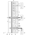
- FIG. 1 is a schematic cross-sectional view showing a configuration of a wafer mounting table 10 equipped with an electrostatic chuck 20.
- FIG. 2 is a schematic cross-sectional view showing a detailed structure of a mounting surface 20a of the electrostatic chuck 20.
- FIG. 2 is an enlarged cross-sectional view of the vicinity of an inclined portion 25 of an embossment 23.
- FIG. 13A and 13B are diagrams showing an embossment 23 according to a modified example.
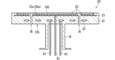
- FIG. 2 is a diagram showing another embodiment of the electrostatic chuck 20.
- ⁇ Wafer placement table> 1 is a schematic cross-sectional view showing the configuration of a wafer mounting table 10 equipped with an electrostatic chuck 20 according to an embodiment of the present invention, taken along the thickness direction of the electrostatic chuck 20.
- the wafer mounting table 10 is also called a susceptor, and is used to fix a semiconductor wafer (wafer), which is one type of workpiece, to the electrostatic chuck 20 when the wafer is subjected to a predetermined process, such as a plasma process.
- the wafer mounting table 10 generally has a configuration in which the electrostatic chuck 20 and the cooling plate 30 are bonded to each other by a bonding layer 40, resulting in a stacked arrangement of the electrostatic chuck 20 and the cooling plate 30.
- Examples of materials for the ESC electrode 21 and the heater electrode 22 include metals such as W, Mo, Ti, Si, and Ru, or carbides or nitrides thereof.
- the cooling plate 30 has an internal flow path 31, and is a part that cools the electrostatic chuck 20 and the wafer electrostatically attracted and fixed to its mounting surface 20a by introducing a coolant (e.g., water) from the outside into the flow path 31.
- a coolant e.g., water
- the flow path 31 has one continuous groove that is spirally arranged in a plan view so that substantially the entire area of the electrostatic chuck 20 is cooled.
- the flow path 31 may have multiple independent open ring-shaped grooves that are concentrically arranged in a plan view.
- the cooling plate 30 is preferably made of a metal material such as aluminum, but ceramics or a composite material of metal and ceramics may also be used.
- the bonding between the electrostatic chuck 20 and the cooling plate 30 by the bonding layer 40 is achieved by, for example, performing heat and pressure bonding on a laminate obtained by bonding the ceramic plate-shaped member constituting the electrostatic chuck 20 and the member constituting the cooling plate 30 with an adhesive layer such as a resin adhesive or adhesive sheet, metal brazing material, or ceramic bond, while heating and pressurizing the laminate at a predetermined temperature.
- the wafer mounting table 10 further includes a first power supply unit 50 that supplies power to the ESC electrode 21, and a second power supply unit 60 that supplies power to the heater electrode 22.
- the first power supply unit 50 is provided along the stacking direction of the electrostatic chuck 20 and the cooling plate 30, and includes a power supply terminal 51, an insulating member (sleeve) 52 surrounding the power supply terminal 51, and a connection portion 53 provided at one end of the power supply terminal 51 and connected to the ESC electrode 21.
- the first power supply unit 50 is inserted into the through hole 33, and the other end side is exposed to the outside. And, at the other end side, the power supply terminal 51 is electrically connected to an external ESC power supply 70.
- a DC voltage is applied from the ESC power supply 70 to the ESC electrode 21 through the power supply terminal 51 and the connection part 53, so that the wafer is electrostatically attracted to the mounting surface 20a.
- the second power supply unit 60 includes a power supply terminal 61, an insulating member (sleeve) 62 surrounding the power supply terminal 61, and a connection portion 63 provided at one end of the power supply terminal 61 and connected to the heater electrode 22.
- the second power supply unit 60 is inserted into a through hole 34 provided in the cooling plate 30, and is exposed to the outside at the other end. At the other end, the power supply terminal 61 is electrically connected to an external heater power source 80.
- the wafer placed on the mounting surface 20a is electrostatically attracted and fixed by applying a voltage to the ESC electrode 21, and then heating is performed in parallel with the application of current to the heater electrode 22 and the circulating supply of a coolant to the flow path 31, thereby balancing heating and cooling and allowing the wafer to be heated with a predetermined temperature distribution.
- the wafer mounting table 10 can be manufactured, for example, by preparing an electrostatic chuck 20 in which an ESC electrode 21 and a heater electrode 22 are embedded, and a cooling plate 30, bonding the electrostatic chuck 20 and the cooling plate 30 with a bonding layer 40, and then embedding a first power supply part 50 and a second power supply part 60.
- the electrostatic chuck 20 can be produced, for example, by hot-pressing and firing a green sheet compact formed by stacking and bonding multiple ceramic green sheets, including a ceramic green sheet on which an electrode pattern for the ESC electrode 21 is printed and formed, and a ceramic green sheet on which an electrode pattern for the heater electrode 22 is printed and formed.
- the mounting surface 20a of the electrostatic chuck 20 after the hot press sintering is subjected to an embossing process (roughness process) described below to provide a large number of convex portions (protrusions).
- the cooling plate 30 can also be manufactured using techniques such as cutting bulk metal, gel casting, or other casting methods.
- ⁇ Details of the placement surface> 2 is a schematic cross-sectional view taken along the thickness direction of the electrostatic chuck 20, showing a detailed structure of the mounting surface 20a of the electrostatic chuck 20. Note that Fig. 2 also shows how the wafer 100 is mounted on the mounting surface 20a.
- the mounting surface 20a is shown as being uniformly flat, but in reality, the mounting surface 20a of the electrostatic chuck 20 according to an embodiment of the present invention has an uneven structure consisting of a large number (plurality) of convex portions 23 spaced apart two-dimensionally at a predetermined pitch p, and concave portions 26 between the convex portions 23.
- the convex portions 23 are also referred to as embossments 23, and the surfaces of the concave portions 26 are also referred to as bottom surfaces 26a.
- the pitch p is set to approximately 2 mm to 20 mm.
- the embossment 23 has a flat portion 24 and an inclined portion 25.
- the flat portion 24 is a portion having a flat surface 24a.
- the flat surface 24a is substantially perpendicular to the thickness direction of the electrostatic chuck 20, is flat, and has a uniform height h (vertical distance from the bottom surface 26a of the recess 26).
- the flat surface 24a and the bottom surface 26a of the recess 26 may include minute irregularities that inevitably occur during manufacturing. Therefore, the height h may be, for example, the difference between the roughness center lines of the flat surface 24a and the bottom surface 26a.
- the roughness center lines of the flat surface 24a and the bottom surface 26a may be the average values of the measured values at multiple points measured by the method specified in JIS B 0601:1994 and JIS B 0031:1994.
- the height h is about 10 ⁇ m to 50 ⁇ m.
- the inclined portion 25 is located around the flat portion 24 when the support surface 20a is viewed in a plan view, and is a portion whose height (vertical distance from the bottom surface 26a of the recess 26) decreases continuously or intermittently from the flat portion 24 toward the recess 26.
- each embossment 23 forms a circle with a diameter d1 at the center of the embossment 23 in plan view, and each embossment 23 itself also forms a circle with a diameter d2 in plan view.
- the inclined portion 25 forms a ring shape with a width w in plan view.
- the upper surface 25a of the inclined portion 25 forms a linear tapered shape in cross section.
- An inclined portion 25 with an upper surface 25a that forms a linear tapered shape in cross section in this manner is sometimes specifically referred to as a tapered portion 25.
- the diameter d1 is about 0.5 mm to 3 mm, the same as a conventional embossment that does not have an inclined portion 25.
- the mounting surface 20a has such an uneven structure, when the wafer 100 is placed on the electrostatic chuck 20, only the flat portion 24 of the embossment 23 actually comes into contact with the wafer 100 and directly supports the wafer 100 downward. Note that a cooling gas for cooling the wafer 100 may be flowed between the wafer 100 and the inclined portion 25 and the recessed portion 26, which do not come into contact with the wafer 100.
- JR force Johnsen-Rahbek force
- the force that contributes to the suction and fixation of the wafer 100 is not limited to the JR force Fj; the spatial Coulomb force Fc from a portion that is not in contact with the wafer 100 but is in close proximity also contributes to suction.
- the spatial Coulomb force Fc is made up of the inclined portion spatial Coulomb force Ft acting between all of the inclined portions 25 (the upper surfaces 25a) and the wafer 100, and the bottom surface spatial Coulomb force Fb acting between the recessed portions 26 (the entire bottom surface 26a) and the wafer 100.
- the spatial Coulomb force Fc is also referred to as the total spatial Coulomb force Fc.
- the inclined portion spatial Coulomb force Ft is inversely proportional to the distance between the inclined portion 25 and the wafer 100
- the bottom surface spatial Coulomb force Fb is inversely proportional to the distance between the bottom surface 26a and the wafer 100.
- the pitch p of the embossments 23 and the planar size (diameter) d1 and height h of the flat portion 24 are all constant, and the warping of the wafer 100 can be ignored, as long as there is always a recess 26 between adjacent embossments 23, the greater the width w of the inclined portion 25, the greater the value of the inclined portion spatial Coulomb force Ft will be compared to the bottom surface spatial Coulomb force Fb, and as a result, the total spatial Coulomb force Fc and thus the overall suction force F will increase.
- the total adsorption force F can also be increased by providing an inclined portion 25 in each embossment 23 and allowing the spatial Coulomb force Ft to act.
- the contact area between the wafer 100 and the electrostatic chuck 20 will increase, and therefore particles will be more likely to be generated.
- the inclined portion 25 does not come into contact with the wafer 100, even if the inclined portion 25 is provided, particles will not be more likely to be generated.
- the electrostatic adsorption force between the wafer 100 and the electrostatic chuck 20 can be improved without making particles more likely to be generated.
- the effect of providing the inclined portion 25 on the embossment 23 can be evaluated based on the angle ⁇ between the upper surface 25a and the thickness direction of the electrostatic chuck 20 (hereinafter referred to as the inclination angle).
- the preferred range of inclination angle ⁇ when inclined portion 25 is provided on embossment 23 is set to be 65 degrees or more, where the total adhesive force increases by 1% or more compared to when inclined portion 25 is not provided. This is because it is believed that there is a significant increase in total adhesive force F compared to when inclined portion 25 is not provided.
- Table 1 also shows that even if inclination angle ⁇ is set to, for example, about 30 degrees, there is almost no effect of increasing adhesive force.
- embossments 23 on the electrostatic chuck 20 may have an inclined portion 25 as shown in FIG. 3.
- embossment 23 that has only one of the curved portion 251 or the curved portion 252.
- the electrostatic attraction force of the electrostatic chuck can be increased without increasing the contact area between the workpiece and the electrostatic chuck by providing an inclined portion that forms an angle of 65 degrees or more and 84 degrees or less with respect to the thickness direction of the electrostatic chuck around the flat portion of each embossment.
- the inclination angle ⁇ of the inclined portion 25 of each embossment 23 provided on the mounting surface 20a of the electrostatic chuck 20 does not need to be the same, and may be different depending on the position of each embossment 23 when the electrostatic chuck 20 is viewed in a plane.
- FIG. 4 is a diagram showing an embossment 23 according to a modified example having an inclined portion 25 of such a shape. More specifically, FIG. 4 is a schematic enlarged cross-sectional view along the thickness direction of the electrostatic chuck 20 in the vicinity of the inclined portion 25.
- the inclined portion 25 is provided in a multi-stage shape consisting of multiple steps 25s. That is, the height of the inclined portion 25 changes intermittently from the flat portion 24 toward the recess 26.
- the inclined line 25b passing through the edge portion of each step 25s in the cross section can be treated in the same way as the straight line formed by the cross section of the upper surface 25a of the tapered inclined portion 25 shown in FIG. 2, for example. That is, the angle between the inclined line 25b and the thickness direction of the electrostatic chuck 20 corresponds to the inclination angle ⁇ .
- embossment 23 having a multi-stage inclined portion 25 consisting of multiple steps 25s can be achieved, for example, by laser processing.
- the ceramic shaft 14 is preferably made of the same insulating ceramic as the ceramic plate 12, and is bonded to the other main surface 12b of the ceramic plate 12 by solid-state bonding or diffusion bonding.
- an ESC electrode 21 for electrostatically attracting a wafer and a heater electrode 22 for heating the wafer are embedded in the ceramic plate 12.
- electricity is passed to the ESC electrode 21 and the heater electrode 22 through rod-shaped power supply terminals 51 and 61 inserted into the internal space of the hollow ceramic shaft 14.
- the power supply terminal 51 is also called the ESC rod 51
- the power supply terminal 61 is also called the heater rod 61.
- the electrostatic chuck 20 having the above configuration is also bonded to the cooling plate 30 by a bonding layer 40 (not shown in FIG. 5) to form the wafer mounting table 10, similar to the electrostatic chuck 20 in FIG. 1.
- the ceramic plate 12 shown in FIG. 5 has multiple lift pin holes 16 penetrating in the thickness direction. More specifically, the lift pin holes 16 are provided in a manner that also penetrates the bonding layer 40 and the cooling plate 30, and are holes through which lift pins (not shown) for lifting the wafer 100 placed on the placement surface 20a from below can be inserted from below the wafer placement table 10. Although not shown in FIG. 1, the wafer placement table 10 shown in FIG. 1 also has multiple lift pin holes.
- the electrostatic adsorption force of the electrostatic chuck can be increased without increasing the contact area between the workpiece and the electrostatic chuck.
Landscapes
- Physics & Mathematics (AREA)
- Electromagnetism (AREA)
- Chemical & Material Sciences (AREA)
- Engineering & Computer Science (AREA)
- Ceramic Engineering (AREA)
- Container, Conveyance, Adherence, Positioning, Of Wafer (AREA)
- Drying Of Semiconductors (AREA)
- Jigs For Machine Tools (AREA)
Abstract
内部に埋設された電極に電圧を印加することによって載置面に載置された被加工物を静電吸着固定する静電チャックにおいて、載置面が、所定のピッチにて二次元的に離隔配置された複数の凸部と前記凸部の間の平坦な凹部とからなる凹凸構造を有してなり、凸部が、静電チャックの厚み方向に対して垂直でかつ高さが均一な平坦面を有する平坦部と、平坦部の周囲に位置し、平坦部から凹部に向かうにつれて高さが小さくなる傾斜部と、を備え、静電チャックの厚み方向に対する傾斜部の上面の傾斜角が65度以上84度以下である、ようにした。
Description
本発明は、ウエハなどの被加工物を静電吸着固定する静電チャックに関し、特にその載置面の形状に関する。
半導体製造プロセスにおいて用いられる、プラズマエッチング装置などのエッチング装置や、PVD装置、CVD装置、イオンプレーティング装置などの成膜装置において、被加工物の固定に静電吸着力を利用した静電チャックが広く用いられている。こうした静電チャックとして、例えば半導体ウエハなどの板状の被加工物が載置される載置面を、複数の凸部(突起)を備える凹凸面とし、凸部にて被加工物を支持するとともに、凹部に冷却ガスを流すことができるように構成されたものが、すでに公知である(例えば、特許文献1および特許文献2参照)。
特許文献1には、載置面の凸部が柱状、円錐台状、半球状である静電チャックが、開示されてなる。
また、特許文献2には、載置面の突起部が、先端に位置し緩やかな曲面で盛り上がっている頂面を含む先端部と、底面側から先端部に向かうほど断面直径が小さい柱部と、柱部と底面とを緩やかな曲線で接続する裾野部とを有する態様が、開示されている。
特許文献1および特許文献2に開示されているような静電チャックにおいては、被加工物と載置面の凸部とが擦れることによってパーティクルが発生することがある。係るパーティクルの発生は、不良発生の要因となるので、可能な限り低減することが望ましい。被加工物と突起との接触面積が小さいほど、パーティクルは発生しにくいが、係る接触面積を小さくしすぎると、吸着力が不足する。吸着力が不足していると、例えば、凹部を流れる冷却用のガスによりウエハが持ち上げられてしまうことがある。
本発明は上記課題に鑑みてなされたものであり、接触面積を増大させることなく被加工物との吸着力が増大された静電チャックを実現することを、目的とする。
上記課題を解決するため、本発明の第1の態様は、内部に埋設されたESC電極に電圧を印加することによって載置面に載置された被加工物を静電吸着固定する静電チャックであって、前記載置面が、所定のピッチにて二次元的に離隔配置された複数の凸部と前記凸部の間の平坦な凹部とからなる凹凸構造を有してなり、前記凸部が、前記静電チャックの厚み方向に対して垂直でかつ高さが均一な平坦面を有する平坦部と、前記平坦部の周囲に位置し、前記平坦部から前記凹部に向かうにつれて高さが小さくなる傾斜部と、を備え、前記静電チャックの厚み方向に対する前記傾斜部の上面の傾斜角が65度以上84度以下である、ことを特徴とする。
本発明の第2の態様は、第1の態様に係る静電チャックであって、前記凸部は断面視テーパ状をなしている、ことを特徴とする。
本発明の第3の態様は、第2の態様に係る静電チャックであって、前記凸部は前記平坦部および前記凹部の少なくとも一方と曲面にて連続している、ことを特徴とする。
本発明の第4の態様は、第1ないし第3の態様のいずれかに係る静電チャックであって、前記平坦面が平面視円形状であり、前記傾斜部が平面視円環状である、ことを特徴とする。
本発明の第5の態様は、第1ないし第4の態様のいずれかに係る静電チャックであって、前記平坦面の前記凹部からの高さが10μm~50μmである、ことを特徴とする。
本発明の第6の態様は、サセプタであって、第1ないし第5の態様のいずれかに係る静電チャックと、前記静電チャック内部に埋設されてなるヒータ電極と、前記静電チャックに接合されてなり、内部に設けられた流路に冷媒が循環供給されることにより、前記被加工物の冷却が可能な冷却板と、を備えることを特徴とする。
本発明の第7の態様は、サセプタであって、第1ないし第5の態様のいずれかに係る静電チャックと、前記静電チャック内部に埋設されてなるヒータ電極と、前記静電チャックに取り付けられてなる中空のシャフトと、を備えることを特徴とする。
本発明の第1ないし第7の態様によれば、被加工物と静電チャックとの接触面積を増大させることなく、静電チャックにおける静電吸着力を増大させることができる。
<ウエハ載置台>
図1は、本発明の実施の形態に係る静電チャック20を備えたウエハ載置台10の構成を示す、静電チャック20の厚み方向に沿った模式断面図である。ウエハ載置台10は、サセプタなどとも称され、被加工物の一態様としての半導体ウエハ(ウエハ)に対しプラズマ処理などの所定の処理を行うにあたり、ウエハを静電チャック20にて固定するものである。
図1は、本発明の実施の形態に係る静電チャック20を備えたウエハ載置台10の構成を示す、静電チャック20の厚み方向に沿った模式断面図である。ウエハ載置台10は、サセプタなどとも称され、被加工物の一態様としての半導体ウエハ(ウエハ)に対しプラズマ処理などの所定の処理を行うにあたり、ウエハを静電チャック20にて固定するものである。
ウエハ載置台10は概略、静電チャック20と冷却板30とが、接合層40にて接合されることにより、静電チャック20と冷却板30とが積層配置された構成を有する。
静電チャック20は、Al2O3やAlNなどの絶縁性セラミックスからなる板状(例えば円板状)の部材に、ウエハを静電吸着するためのESC電極(静電チャック電極)21が埋設されたものである。図1に示す静電チャック20にはさらに、ウエハを加熱するためのヒータ電極22が埋設されている。このような静電チャック20は静電チャックヒータとも称される。図1に示す静電チャック20においては、ESC電極21の方がヒータ電極22よりも、載置面20aの近くに埋設されている。静電チャック20においては、接合層40との接合面と反対側の主面が、ウエハの載置される載置面20aとなっている。
ESC電極21およびヒータ電極22の材料としては、W、Mo、Ti、Si、Ruなどの金属、もしくはその炭化物や窒化物などが例示される。
冷却板30は、内部に流路31を備えており、該流路31に対し外部から冷媒(例えば水)を導入することによって静電チャック20さらにはその載置面20aに静電吸着固定されたウエハを冷却する部位である。流路31は、静電チャック20の略全域が冷却されるよう、一の連続する溝部が平面視で渦巻き状に設けられるのが好適な一例である。あるいは、複数の独立した開環状の溝部が平面視で同心円状に設けられる態様であってもよい。
冷却板30の材料としては、アルミニウムなどの金属材料を用いるのが好適であるが、セラミックスや、金属とセラミックスとの複合材料が用いられる態様であってもよい。
流路31の少なくとも一つの箇所に、フィン32が突設されていてもよい。フィン32は、その配置箇所における冷媒の流速を増大させ、局所的に冷却効率を高める作用を有する。フィン32の形状およびサイズは、その配置箇所に求められる冷却状況に応じて、適宜に定められる。フィン32は、冷却板30の材料と同じ材料にて設けられていてもよいし、冷却板30とは異なる材料にて設けられていてもよい。なお、フィン32が設けられない態様であってもよい。
接合層40による静電チャック20と冷却板30との接合は、例えば、静電チャック20を構成するセラミックスの板状部材と冷却板30を構成する部材とを樹脂製の接着剤あるいは接着シート、金属ロウ材、セラミックボンドなどの接着層にて接着することによって得られる積層体を対象に、所定の温度で加熱しつつ加圧する加熱加圧接合を行うことにより、実現されてなる。
また、ウエハ載置台10にはさらに、ESC電極21に対する給電を担う第1給電部50と、ヒータ電極22に対する給電を担う第2給電部60とが備わっている。
第1給電部50は、静電チャック20と冷却板30との積層方向に沿って設けられてなり、給電端子51と、該給電端子51を囲繞する絶縁部材(スリーブ)52と、給電端子51の一方端部に設けられ、ESC電極21に接続される接続部53とを備える。第1給電部50は、貫通穴33に挿嵌させられてなり、他方端部側において外部に露出してなる。そして、係る他方端部側において給電端子51が外部に備わるESC電源70と電気的に接続されてなる。
ウエハ載置台10においては、静電チャック20の載置面20aにウエハが載置された状態で、ESC電源70にて給電端子51および接続部53を通じてESC電極21に直流電圧が印加されることにより、ウエハが載置面20aに静電吸着される。
また、第2給電部60は、給電端子61と、該給電端子61を囲繞する絶縁部材(スリーブ)62と、給電端子61の一方端部に設けられ、ヒータ電極22に接続される接続部63とを備える。第2給電部60は、冷却板30に備わる貫通穴34に挿嵌させられてなり、他方端部側において外部に露出してなる。そして、係る他方端部側において給電端子61が外部に備わるヒータ電源80と電気的に接続されてなる。
ウエハ載置台10においては、ヒータ電源80にて給電端子61および接続部63を通じてヒータ電極22に通電がなされることにより、ウエハ載置台10さらにはウエハが加熱される。
また、蓋部30bの所定位置には、該蓋部30bが基部30aに固定された状態において流路31に連通する冷媒出入口35が貫通してなる。なお、図1においては図示の簡単のため、冷媒出入口35を1つのみ示しているが、実際には、冷媒出入口35は、流路31を構成する溝部の両端部にそれぞれ1つずつ設けられる。それぞれの冷媒出入口35は、流路31に対し冷媒を循環供給させるチラーユニット90に接続されてなる。
以上のような構成を有するウエハ載置台10においては、載置面20aに載置したウエハをESC電極21に対する電圧の印加によって静電吸着固定させた状態で、ヒータ電極22に対する通電による加熱と流路31に対する冷媒の循環供給とを並行して行うことにより、加熱と冷却とをバランスさせることによって、所定の温度分布にてウエハを加熱することができるようになっている。
係るウエハ載置台10は、例えば、ESC電極21とヒータ電極22とが埋設された静電チャック20と、冷却板30とをそれぞれに用意したうえで、静電チャック20と冷却板30とを接合層40にて接合し、続いて第1給電部50および第2給電部60を埋設するという手順にて、製造可能である。
静電チャック20の作製は例えば、ESC電極21用の電極パターンが印刷形成されたセラミックスグリーンシートと、ヒータ電極22用の電極パターンが印刷形成されたセラミックスグリーンシートとを含む複数のセラミックスグリーンシートを積層接着することで形成したグリーンシート成形体を、ホットプレス焼成することにより行える。
ただし、本実施の形態においては、係るホットプレス焼成後の静電チャック20の載置面20aに対し、後述するエンボス加工(凹凸加工)を施し、多数の凸部(突起)を設けるようにする。
また、冷却板30は、バルク金属の切削加工や、ゲルキャスティングその他の鋳造などの手法にて、作製することができる。
<載置面の詳細>
図2は、静電チャック20の載置面20aの詳細構造を示す、静電チャック20の厚み方向に沿った模式断面図である。なお、図2においては、ウエハ100が載置面20aに載置される様子も併せて示している。
図2は、静電チャック20の載置面20aの詳細構造を示す、静電チャック20の厚み方向に沿った模式断面図である。なお、図2においては、ウエハ100が載置面20aに載置される様子も併せて示している。
図1においては図示の簡単のため、載置面20aが一様に平坦であるように示されているが、実際には、本発明の実施の形態に係る静電チャック20の載置面20aは、所定のピッチpにて二次元的に離隔配置された多数の(複数の)凸部23と、係る凸部23の間の凹部26とからなる、凹凸構造を有してなる。以降においては、凸部23をエンボス23とも称し、凹部26の表面を底面26aとも称する。なお、ピッチpは2mm~20mm程度に設定される。
エンボス23は、平坦部24と傾斜部25とを有する。平坦部24は、平坦面24aを有する部位である。平坦面24aは実質的に、静電チャック20の厚み方向に対して垂直でかつ平坦でありかつ均一な高さ(凹部26の底面26aからの垂直距離)hを有する。ただし、平坦面24aおよび凹部26の底面26aは製造時に不可避的に生じる微細な凹凸を含んでも良い。それゆえ、高さhは例えば、平坦面24aおよび底面26aそれぞれの粗さ中心線の差であってもよい。平坦面24aおよび底面26aのそれぞれの粗さ中心線は、JIS B 0601:1994, JIS B 0031:1994にて定められた手法で測定された複数個所における測定値の平均値であってもよい。高さhは10μm~50μm程度とされる。
傾斜部25は、載置面20aを平面視した場合において平坦部24の周囲に位置し、平坦部24から凹部26に向かうにつれて連続的にあるいは断続的に高さ(凹部26の底面26aからの垂直距離)が小さくなる部位である。
好適な一態様においては、それぞれのエンボス23の平坦面24aが、平面視において当該エンボス23の中心にて直径d1の円形をなしており、個々のエンボス23そのものも、平面視において直径d2の円形をなしている。これに伴い、傾斜部25は、平面視において幅wの円環状をなしている。また、傾斜部25の上面25aは、断面視直線状のテーパ状をなしている。このように上面25aが断面視直線状のテーパ状をなす傾斜部25を特に、テーパ部25と称することがある。直径d1は、傾斜部25を有さない従来のエンボスと同様、0.5mm~3mm程度とされる。
載置面20aがこのような凹凸構造を有することにより、静電チャック20にウエハ100が載置された状態において実際にウエハ100と接触し、ウエハ100を直接に下方支持するのは、エンボス23の平坦部24のみとなっている。なお、ウエハ100と接触しない傾斜部25および凹部26とウエハ100との間には、ウエハ100を冷却するための冷却ガスが流される場合がある。
ウエハ100が静電チャック20に吸着固定される際には、上述したように、ESC電源70からESC電極21に対し直流電圧が印加される。これにより、ウエハ100と該ウエハ100に接触している全てのエンボス23の平坦部24との間にJohnsen-Rahbek力(以下、JR力と称する)Fjが生じる。
ただし、ウエハ100の吸着固定に寄与する力は係るJR力Fjのみではなく、ウエハ100と非接触ではあるが近接する部位からの空間クーロン力Fcも、吸着に寄与する。具体的には、空間クーロン力Fcは、全ての傾斜部25(の上面25a)とウエハ100との間に作用する傾斜部空間クーロン力Ftと、凹部26(の底面26aの全体)とウエハ100との間に作用する底面空間クーロン力Fbとからなる。以降、空間クーロン力Fcを合計空間クーロン力Fcとも称する。
すなわち、ウエハ100が静電チャック20に吸着固定される際の全体吸着力Fは、
F=Fj+Fc=Fj+Ft+Fb
にて表される。
F=Fj+Fc=Fj+Ft+Fb
にて表される。
係る場合において、傾斜部空間クーロン力Ftは傾斜部25とウエハ100との距離に反比例し、底面空間クーロン力Fbは底面26aとウエハ100との距離に反比例する。それゆえ、エンボス23のピッチpと平坦部24の平面サイズ(直径)d1および高さhがいずれも一定であり、かつウエハ100の撓みが無視できる場合、隣り合うエンボス23の間に凹部26が必ず存在する限りにおいては、傾斜部25の幅wが大きいほど傾斜部空間クーロン力Ftの値が底面空間クーロン力Fbに比して十分に大きくなり、結果として合計空間クーロン力Fcさらには全体吸着力Fが増大する、という関係が成立する。
このことは、個々のエンボス23における平坦部24の平面サイズ(直径)d1を増大させてJR力Fjを増大させる代わりに、個々のエンボス23に傾斜部25を設けて傾斜部空間クーロン力Ftを作用させることによっても、全体吸着力Fを増大させることができることを意味する。
しかも、平坦部24の平面サイズd1を増大させた場合、ウエハ100と静電チャック20との接触面積が増大することになり、それゆえ、パーティクルが発生しやすくなるが、傾斜部25はウエハ100とは接触しないため、傾斜部25を設けたとしても、パーティクルが発生しやすくなることはない。
換言すれば、エンボス23に傾斜部25を設けることによって、パーティクルをより発生しやすくすることなく、ウエハ100と静電チャック20との静電吸着力を向上させることができる。
傾斜部25の上面25aがテーパ状をなしている場合、エンボス23に傾斜部25を設けることの効果は、上面25aと、静電チャック20の厚み方向とのなす角(以下、傾斜角)αの大小によって、評価することができる。
このように傾斜部25がテーパ状をなしている静電チャック20を対象に、傾斜角α(テーパ角αとも称する)の値を種々に違えつつ底面空間クーロン力Fbと傾斜部空間クーロン力Ftとをシミュレーションしたときの結果を、あらかじめ実験的に求めたJR力Fjと、当該シミュレーション結果から求まる合計空間クーロン力Fcと、JR力Fjと合計空間クーロン力Fcとの和である全体吸着力Fと、該全体吸着力Fの増加率と、アスペクト比w/hとともに、表1に一覧にして示す。

なお、シミュレーションに際しては、エンボス23の平面サイズ(直径)d1を0.5mmとし、エンボス23の平坦部24の高さhを20μmとし、載置面20aの全平面面積に対する、エンボス23の平坦部24の平坦面24aの合計面積の比である、ウエハ100の接触面積率を、3%とし、静電吸着に際してESC電源70がESC電極21に対し印加する直流電圧の値を、500Vとしている。
また、あらかじめ実験的に求めた、エンボス23が傾斜部25を有さない、すなわち傾斜角α=0度である静電チャック20についての全体吸着力F(26.2Torr)とJR力Fj(18Torr)とを、利用している。それゆえ、厳密にいえば、表1における傾斜角α=0度のときのそれぞれの力の値は実験値である。そして、全体吸着力Fの増加率としては、傾斜角α=0度のときの全体吸着力Fを基準とした増加率を示している。
表1からわかるように、傾斜角αが大きくなるほど、全体吸着力Fの増加率は大きくなる傾向がある。
本実施の形態においては、傾斜部25を設けない場合に比して全体吸着力が1%以上増加する、傾斜角αが65度以上という範囲が、エンボス23に傾斜部25を設ける場合の傾斜角αの好ましい範囲であるとする。傾斜部25を設けない場合に比して、全体吸着力Fに有意な増大があると考えられるからである。なお、表1は、傾斜角αを例えば30度程度設けたとしても、吸着力を増大させる効果はほとんど得られないことも示している。
ただし、傾斜角αは84度以下とする。傾斜角αが84度を上回ると、ウエハ100を吸着固定した際に、ウエハ100の撓みによって傾斜部25にもウエハ100が接触してしまうおそれが高まり、好ましくないからである。
すなわち、本実施の形態においては、静電チャック20の表面に多数のエンボス23にて凹凸を付与するに際し、それぞれのエンボス23の平坦部24の周囲に、静電チャック20の厚み方向に対し65度以上84度以下の傾斜角αをなすように傾斜部25を設けることによって、ウエハ100との接触面積を増大させることなく、静電チャック20に対するウエハ100の静電吸着力を増大させるようにする。なお、この65度以上84度以下という傾斜角αの範囲は概ね、傾斜角αの正接(tan)に相当するアスペクト比w/hが2.1以上9.5以下という範囲に相当する。
こうした、静電チャック20を用いることによる静電吸着力の増大という効果は、ウエハ100以外の被加工物が載置される場合についても、同様に得ることができる。
なお、エンボス23に傾斜部25を設けることによって、平坦部24の平坦面24aの面積を増やすことなく、換言すれば、ウエハ100との接触面積を傾斜部25を設けない場合から増やすことなく、吸着力を増大させることができるということは、別の見方をすれば、平坦面24aの面積を小さくしながら傾斜部25を設けることにより、ウエハ100との接触面積を減少させつつ、傾斜部25を設けない場合と同程度の吸着力得ることも可能である、ということでもある。
<傾斜部の微細形状例>
図3は、あるエンボス23の傾斜部25の近傍についての、静電チャック20の厚み方向に沿った模式的な拡大断面図である。
図3は、あるエンボス23の傾斜部25の近傍についての、静電チャック20の厚み方向に沿った模式的な拡大断面図である。
図2においては、断面視直線状である傾斜部25の上面25aが平坦部24の平坦面24aと凹部26の底面26aと連続する様子を示していた。しかしながら、実際の傾斜部25を微視的にみた場合、図3に示すように、その上面25aが、平坦な斜面である断面視直線状の中央部250と、その両端の曲面状(断面視曲線状の)曲面部251および252とから、構成され、曲面部251が凹部26の底面26aと滑らかに連続し、曲面部252が平坦部24の平坦面24aと滑らかに連続していてもよい。
曲面部251が形成される場合、エンボス23と凹部26との境界部分にパーティクルが残存しにくくなる。また、曲面部252が形成される場合、ウエハ100が接触する際にエンボス23が擦れて削られることが起こりにくくなる。
ただし、曲面部251および252の形成範囲は通常、傾斜部25の両端のごくわずかな範囲であるので、上面25aの中央部250、凹部26の底面26a、および平坦部24の平坦面24aの仮想的な延長面をそれぞれ、図2における傾斜部25の上面25a、凹部26の底面26a、および平坦部24の平坦面24aとみなして差し支えない。
図3の断面図においては、直線L0が中央部250の仮想的な延長面に相当し、直線L1が底面26aの仮想的な延長面に相当し、直線L2が平坦面24aの仮想的な延長面に相当する。そして、直線L0と直線L1との交点P1と、直線L0と直線L2との交点P2との垂直距離および水平距離をそれぞれ、高さhおよび幅wとみなすことができる。より詳細には、交点P1は中央部250の仮想的な延長面と底面26aの仮想的な延長面の交線の断面に相当し、交点P2は中央部250の仮想的な延長面と平坦面24aの仮想的な延長面の交線の断面に相当する。また、静電チャック20の厚み方向と直線L0とがなす角を傾斜角αとみなすことができる。
静電チャック20に備わる全部あるいは一部のエンボス23が、図3に示すような傾斜部25を有する態様であってもよい。あるいは、曲面部251または曲面部252の一方のみを有するエンボス23が存在していてもよい。
テーパ状その他の形状の傾斜部25を有するエンボス(凸部)23と、凹部26とからなる凹凸構造の形成は、例えば、静電チャック20を構成するセラミックスの板状部材と冷却板30を構成する部材とを接合するに先立って、前者のセラミックス部材の平坦な表面に対し、サンドブラスト加工、マシニング加工、超音波加工、レーザ加工、研磨加工などの種々の公知の加工手法による加工を、適宜に組み合わせつつ施すことによって、行うことができる。
以上、説明したように、本実施の形態によれば、例えば半導体ウエハなどの被加工物を静電吸着固定する静電チャックの表面に、接触面積低減のために多数のエンボスにて凹凸を付与するに際し、それぞれのエンボスの平坦部の周囲に、静電チャックの厚み方向に対し65度以上84度以下の角をなす傾斜部を設けることによって、被加工物と静電チャックとの接触面積を増大させることなく、静電チャックにおける静電吸着力を増大させることができる。
<変形例>
静電チャック20の載置面20aに設ける個々のエンボス23の傾斜部25の傾斜角αは、同じである必要はなく、静電チャック20を平面視した場合における個々のエンボス23の位置によって、違えられてもよい。
静電チャック20の載置面20aに設ける個々のエンボス23の傾斜部25の傾斜角αは、同じである必要はなく、静電チャック20を平面視した場合における個々のエンボス23の位置によって、違えられてもよい。
例えば、中心部に位置するエンボス23における傾斜角αよりも、外周部に位置するエンボス23における傾斜角αを大きくしてもよい。係る場合、外周部のエンボス23の方が中心部のエンボス23よりも吸着力が大きくなるため、吸着対象であるウエハに反りがあったとしても、外周部においてウエハが載置面20aから離隔してしまうことを抑制し、該ウエハを好適に固定することができる。
上述の実施の形態においては主として、傾斜部25の高さが平坦部24から凹部26に向かうにつれて連続的に小さくなる構成を対象に説明を行い、より具体的には傾斜部25がテーパ状をなしている構成を例示していたが、先にも述べたように、傾斜部25の高さは断続的に変化する態様であってもよい。
図4は、そのような形状の傾斜部25を備えた、変形例に係るエンボス23を示す図である。より具体的には、図4は、係る傾斜部25の近傍の、静電チャック20の厚み方向に沿った模式的な拡大断面図である。図4に示すエンボス23においては、傾斜部25が、複数のステップ25sからなる多段状に設けられている。すなわち、傾斜部25の高さが、平坦部24から凹部26に向かうにつれて断続的に変化している。係る場合においては、断面において個々のステップ25sのエッジ部分を通る傾斜線25bを、例えば図2に示したテーパ状をなす傾斜部25の上面25aの断面がなす直線と同様に取り扱うことができる。すなわち、傾斜線25bと静電チャック20の厚み方向とのなす角が傾斜角αに相当する。
このような、複数のステップ25sからなる多段状の傾斜部25を有するエンボス23の形成は、例えばレーザ加工によって実現可能である。
係る多段状の傾斜部25を有するエンボス23にて載置面20aに凹凸構造が形成された静電チャック20であっても、被加工物と静電チャック20との接触面積を増大させることなく、静電チャック20における静電吸着力を増大させる、という効果を得ることができる。
<静電チャックの別態様>
図5は、図1に示すものとは別態様の静電チャック20の、厚み方向に沿った模式断面図である。図5に示す静電チャック20は概略、図1に示した静電チャック20と同様の絶縁性セラミックスからなる板状(例えば円板状)のセラミックプレート12と、該セラミックプレート12に接合された中空のセラミックシャフト14から構成される。
図5は、図1に示すものとは別態様の静電チャック20の、厚み方向に沿った模式断面図である。図5に示す静電チャック20は概略、図1に示した静電チャック20と同様の絶縁性セラミックスからなる板状(例えば円板状)のセラミックプレート12と、該セラミックプレート12に接合された中空のセラミックシャフト14から構成される。
セラミックプレート12の一方主面12aは、図2と同様の多数の凸部(エンボス)23を備える載置面20aとなっている。図5においては図示を簡略化しているが、係る一方主面12aに備わるエンボス23にも、図2に示したような平坦部24と傾斜部25とが備わっている。すなわち、それぞれのエンボス23の平坦部24の周囲に、静電チャックの厚み方向に対し65度以上84度以下の角をなす傾斜部25が設けられてなる。なお、図5においては、ウエハ100が載置面20aに載置される様子も併せて示している。
セラミックシャフト14は、好ましくはセラミックプレート12と同様の絶縁性セラミックスから構成されてなり、固相接合または拡散接合にてセラミックプレート12の他方主面12bに接合されてなる。
また、セラミックプレート12には、図1に示した静電チャック20と同様に、ウエハを静電吸着するためのESC電極21と、ウエハを加熱するためのヒータ電極22とが埋設されてなる。ただし、これらESC電極21とヒータ電極22への通電は、中空のセラミックシャフト14の内部空間に挿通されたロッド状の給電端子51および61を通じて行われる。なお、図5においてはスリーブ52および62と接続部53および63の図示を省略している。給電端子51はESCロッド51とも称され、給電端子61はヒータロッド61とも称される。
以上のような構成を有する静電チャック20も、図1の静電チャック20と同様に、図5においては図示しない接合層40にて冷却板30と接合されて、ウエハ載置台10を構成する。
加えて、図5に示すセラミックプレート12には、複数のリフトピン穴16が、厚み方向に貫通してなる。より詳細には、リフトピン穴16は、接合層40および冷却板30をも貫通する態様にて設けられるものであり、載置面20aに載置されたウエハ100を下から持ち上げるためのリフトピン(図示せず)を、ウエハ載置台10の下方から挿通させるための穴である。なお、図1においては図示を省略していたが、図1に示したウエハ載置台10においても同様に、複数のリフトピン穴が設けられる。
図5に示した構成の静電チャックを備えるウエハ載置台においても、被加工物と静電チャックとの接触面積を増大させることなく、静電チャックにおける静電吸着力を増大させることができる。
Claims (7)
- 内部に埋設されたESC電極に電圧を印加することによって載置面に載置された被加工物を静電吸着固定する静電チャックであって、
前記載置面が、所定のピッチにて二次元的に離隔配置された複数の凸部と前記凸部の間の平坦な凹部とからなる凹凸構造を有してなり、
前記凸部が、
前記静電チャックの厚み方向に対して垂直でかつ高さが均一な平坦面を有する平坦部と、
前記平坦部の周囲に位置し、前記平坦部から前記凹部に向かうにつれて高さが小さくなる傾斜部と、
を備え、
前記静電チャックの厚み方向に対する前記傾斜部の上面の傾斜角が65度以上84度以下である、
ことを特徴とする静電チャック。 - 請求項1に記載の静電チャックであって、
前記凸部は断面視テーパ状をなしている、
ことを特徴とする静電チャック。 - 請求項2に記載の静電チャックであって、
前記凸部は前記平坦部および前記凹部の少なくとも一方と曲面にて連続している、
ことを特徴とする静電チャック。 - 請求項1ないし請求項3のいずれかに記載の静電チャックであって、
前記平坦面が平面視円形状であり、
前記傾斜部が平面視円環状である、
ことを特徴とする静電チャック。 - 請求項1ないし請求項3のいずれかに記載の静電チャックであって、
前記平坦面の前記凹部からの高さが10μm~50μmである、
ことを特徴とする静電チャック。 - 請求項1ないし請求項3のいずれかに記載の静電チャックと、
前記静電チャック内部に埋設されてなるヒータ電極と、
前記静電チャックに接合されてなり、内部に設けられた流路に冷媒が循環供給されることにより、前記被加工物の冷却が可能な冷却板と、
を備えることを特徴とするサセプタ。 - 請求項1ないし請求項3のいずれかに記載の静電チャックと、
前記静電チャック内部に埋設されてなるヒータ電極と、
前記静電チャックに取り付けられてなる中空のシャフトと、
を備えることを特徴とするサセプタ。
Priority Applications (7)
| Application Number | Priority Date | Filing Date | Title |
|---|---|---|---|
| KR1020247006393A KR20240174866A (ko) | 2023-06-08 | 2023-06-08 | 정전 척 및 서셉터 |
| JP2024505120A JP7639238B1 (ja) | 2023-06-08 | 2023-06-08 | 静電チャックおよびサセプタ |
| CN202380013321.2A CN121359628A (zh) | 2023-06-08 | 2023-06-08 | 静电卡盘及基座 |
| PCT/JP2023/021338 WO2024252613A1 (ja) | 2023-06-08 | 2023-06-08 | 静電チャックおよびサセプタ |
| US18/432,156 US12695398B2 (en) | 2023-06-08 | 2024-02-05 | Electrostatic chuck and susceptor |
| TW113115356A TW202449972A (zh) | 2023-06-08 | 2024-04-25 | 靜電吸盤及基座 |
| JP2025023368A JP2025069465A (ja) | 2023-06-08 | 2025-02-17 | 静電チャックおよびサセプタ |
Applications Claiming Priority (1)
| Application Number | Priority Date | Filing Date | Title |
|---|---|---|---|
| PCT/JP2023/021338 WO2024252613A1 (ja) | 2023-06-08 | 2023-06-08 | 静電チャックおよびサセプタ |
Related Child Applications (1)
| Application Number | Title | Priority Date | Filing Date |
|---|---|---|---|
| US18/432,156 Continuation US12695398B2 (en) | 2023-06-08 | 2024-02-05 | Electrostatic chuck and susceptor |
Publications (1)
| Publication Number | Publication Date |
|---|---|
| WO2024252613A1 true WO2024252613A1 (ja) | 2024-12-12 |
Family
ID=93744226
Family Applications (1)
| Application Number | Title | Priority Date | Filing Date |
|---|---|---|---|
| PCT/JP2023/021338 Ceased WO2024252613A1 (ja) | 2023-06-08 | 2023-06-08 | 静電チャックおよびサセプタ |
Country Status (6)
| Country | Link |
|---|---|
| US (1) | US12695398B2 (ja) |
| JP (2) | JP7639238B1 (ja) |
| KR (1) | KR20240174866A (ja) |
| CN (1) | CN121359628A (ja) |
| TW (1) | TW202449972A (ja) |
| WO (1) | WO2024252613A1 (ja) |
Citations (6)
| Publication number | Priority date | Publication date | Assignee | Title |
|---|---|---|---|---|
| JP2005038931A (ja) * | 2003-07-16 | 2005-02-10 | Toto Ltd | 静電チャック |
| WO2007013619A1 (ja) * | 2005-07-28 | 2007-02-01 | Kyocera Corporation | 試料保持具とこれを用いた試料吸着装置およびこれを用いた試料処理方法 |
| JP2013153171A (ja) * | 2013-02-15 | 2013-08-08 | Panasonic Corp | プラズマ処理装置及びプラズマ処理方法 |
| JP2015008240A (ja) * | 2013-06-26 | 2015-01-15 | 京セラ株式会社 | 吸着部材 |
| JP2017191949A (ja) * | 2014-09-30 | 2017-10-19 | 住友大阪セメント株式会社 | 静電チャック装置 |
| WO2020170514A1 (ja) * | 2019-02-20 | 2020-08-27 | 住友大阪セメント株式会社 | 静電チャック装置 |
Family Cites Families (9)
| Publication number | Priority date | Publication date | Assignee | Title |
|---|---|---|---|---|
| US5903428A (en) * | 1997-09-25 | 1999-05-11 | Applied Materials, Inc. | Hybrid Johnsen-Rahbek electrostatic chuck having highly resistive mesas separating the chuck from a wafer supported thereupon and method of fabricating same |
| CN101978473B (zh) | 2008-03-20 | 2015-11-25 | 应用材料公司 | 具有滚轧成型表面的基座和制造所述基座的方法 |
| JP5225041B2 (ja) | 2008-11-21 | 2013-07-03 | 京セラ株式会社 | 静電チャック |
| JP5454803B2 (ja) | 2010-08-11 | 2014-03-26 | Toto株式会社 | 静電チャック |
| JP2014027207A (ja) | 2012-07-30 | 2014-02-06 | Hitachi Chemical Co Ltd | 誘電体及びこの誘電体を用いた静電チャック |
| US9685356B2 (en) * | 2012-12-11 | 2017-06-20 | Applied Materials, Inc. | Substrate support assembly having metal bonded protective layer |
| JP2015008270A (ja) * | 2013-05-27 | 2015-01-15 | 株式会社村田製作所 | セラミック電子部品 |
| US11031278B2 (en) * | 2016-03-30 | 2021-06-08 | Kyocera Corporation | Suction member |
| JP6646700B2 (ja) | 2018-03-19 | 2020-02-14 | 株式会社不二製作所 | 硬質脆性材料製の被処理成品の表面加工方法 |
-
2023
- 2023-06-08 KR KR1020247006393A patent/KR20240174866A/ko active Pending
- 2023-06-08 WO PCT/JP2023/021338 patent/WO2024252613A1/ja not_active Ceased
- 2023-06-08 JP JP2024505120A patent/JP7639238B1/ja active Active
- 2023-06-08 CN CN202380013321.2A patent/CN121359628A/zh active Pending
-
2024
- 2024-02-05 US US18/432,156 patent/US12695398B2/en active Active
- 2024-04-25 TW TW113115356A patent/TW202449972A/zh unknown
-
2025
- 2025-02-17 JP JP2025023368A patent/JP2025069465A/ja active Pending
Patent Citations (6)
| Publication number | Priority date | Publication date | Assignee | Title |
|---|---|---|---|---|
| JP2005038931A (ja) * | 2003-07-16 | 2005-02-10 | Toto Ltd | 静電チャック |
| WO2007013619A1 (ja) * | 2005-07-28 | 2007-02-01 | Kyocera Corporation | 試料保持具とこれを用いた試料吸着装置およびこれを用いた試料処理方法 |
| JP2013153171A (ja) * | 2013-02-15 | 2013-08-08 | Panasonic Corp | プラズマ処理装置及びプラズマ処理方法 |
| JP2015008240A (ja) * | 2013-06-26 | 2015-01-15 | 京セラ株式会社 | 吸着部材 |
| JP2017191949A (ja) * | 2014-09-30 | 2017-10-19 | 住友大阪セメント株式会社 | 静電チャック装置 |
| WO2020170514A1 (ja) * | 2019-02-20 | 2020-08-27 | 住友大阪セメント株式会社 | 静電チャック装置 |
Also Published As
| Publication number | Publication date |
|---|---|
| JP2025069465A (ja) | 2025-04-30 |
| JP7639238B1 (ja) | 2025-03-04 |
| CN121359628A (zh) | 2026-01-16 |
| TW202449972A (zh) | 2024-12-16 |
| US20240413770A1 (en) | 2024-12-12 |
| JPWO2024252613A1 (ja) | 2024-12-12 |
| KR20240174866A (ko) | 2024-12-17 |
| US12695398B2 (en) | 2026-07-28 |
Similar Documents
| Publication | Publication Date | Title |
|---|---|---|
| TW530367B (en) | Wafer chuck system | |
| TW590852B (en) | Electrostatic chuck having a low level of particle generation and method of fabricating same | |
| US11328907B2 (en) | Electrostatic chuck | |
| JP7657072B2 (ja) | 電極埋設部材、その製造方法、および基板保持部材 | |
| TW202040744A (zh) | 局部加熱之多區域基材支撐座 | |
| CN113994462A (zh) | 静电吸盘 | |
| JP7613992B2 (ja) | 保持装置 | |
| KR102914354B1 (ko) | 웨이퍼 배치대 | |
| US12308220B2 (en) | Wafer placement table | |
| KR102863907B1 (ko) | 웨이퍼 배치대 | |
| KR20170067719A (ko) | 정전 척 장치 | |
| TW202243888A (zh) | 靜電式定位盤及其製造方法 | |
| JP7783391B2 (ja) | ウエハ載置台 | |
| JP7379171B2 (ja) | 保持装置 | |
| JP7639238B1 (ja) | 静電チャックおよびサセプタ | |
| CN115995374B (zh) | 晶片载放台 | |
| JP2025143310A (ja) | 保持装置 | |
| TWI844329B (zh) | 靜電吸盤 | |
| JP7628867B2 (ja) | 保持部材 | |
| US11302560B2 (en) | Electrostatic chuck | |
| JP7373111B2 (ja) | 静電チャック | |
| JP7828782B2 (ja) | 試料保持具 | |
| JP7797336B2 (ja) | 基板固定装置及び基板固定装置の製造方法 | |
| JP7698521B2 (ja) | 保持装置の製造方法 | |
| JP2005277335A (ja) | ウェハ支持部材 |
Legal Events
| Date | Code | Title | Description |
|---|---|---|---|
| WWE | Wipo information: entry into national phase |
Ref document number: 2024505120 Country of ref document: JP |
|
| 121 | Ep: the epo has been informed by wipo that ep was designated in this application |
Ref document number: 23940712 Country of ref document: EP Kind code of ref document: A1 |
|
| NENP | Non-entry into the national phase |
Ref country code: DE |
|
| 122 | Ep: pct application non-entry in european phase |
Ref document number: 23940712 Country of ref document: EP Kind code of ref document: A1 |