WO2024247697A1 - 表示装置および電子機器 - Google Patents
表示装置および電子機器 Download PDFInfo
- Publication number
- WO2024247697A1 WO2024247697A1 PCT/JP2024/017670 JP2024017670W WO2024247697A1 WO 2024247697 A1 WO2024247697 A1 WO 2024247697A1 JP 2024017670 W JP2024017670 W JP 2024017670W WO 2024247697 A1 WO2024247697 A1 WO 2024247697A1
- Authority
- WO
- WIPO (PCT)
- Prior art keywords
- light
- layer
- display device
- lenses
- lens
- Prior art date
- Legal status (The legal status is an assumption and is not a legal conclusion. Google has not performed a legal analysis and makes no representation as to the accuracy of the status listed.)
- Ceased
Links
Images











Classifications
-
- G—PHYSICS
- G02—OPTICS
- G02B—OPTICAL ELEMENTS, SYSTEMS OR APPARATUS
- G02B3/00—Simple or compound lenses
-
- G—PHYSICS
- G09—EDUCATION; CRYPTOGRAPHY; DISPLAY; ADVERTISING; SEALS
- G09F—DISPLAYING; ADVERTISING; SIGNS; LABELS OR NAME-PLATES; SEALS
- G09F9/00—Indicating arrangements for variable information in which the information is built-up on a support by selection or combination of individual elements
- G09F9/30—Indicating arrangements for variable information in which the information is built-up on a support by selection or combination of individual elements in which the desired character or characters are formed by combining individual elements
-
- H—ELECTRICITY
- H10—SEMICONDUCTOR DEVICES; ELECTRIC SOLID-STATE DEVICES NOT OTHERWISE PROVIDED FOR
- H10K—ORGANIC ELECTRIC SOLID-STATE DEVICES
- H10K50/00—Organic light-emitting devices
- H10K50/10—OLEDs or polymer light-emitting diodes [PLED]
-
- H—ELECTRICITY
- H10—SEMICONDUCTOR DEVICES; ELECTRIC SOLID-STATE DEVICES NOT OTHERWISE PROVIDED FOR
- H10K—ORGANIC ELECTRIC SOLID-STATE DEVICES
- H10K50/00—Organic light-emitting devices
- H10K50/80—Constructional details
- H10K50/85—Arrangements for extracting light from the devices
- H10K50/858—Arrangements for extracting light from the devices comprising refractive means, e.g. lenses
-
- H—ELECTRICITY
- H10—SEMICONDUCTOR DEVICES; ELECTRIC SOLID-STATE DEVICES NOT OTHERWISE PROVIDED FOR
- H10K—ORGANIC ELECTRIC SOLID-STATE DEVICES
- H10K59/00—Integrated devices, or assemblies of multiple devices, comprising at least one organic light-emitting element covered by group H10K50/00
- H10K59/10—OLED displays
-
- H—ELECTRICITY
- H10—SEMICONDUCTOR DEVICES; ELECTRIC SOLID-STATE DEVICES NOT OTHERWISE PROVIDED FOR
- H10K—ORGANIC ELECTRIC SOLID-STATE DEVICES
- H10K59/00—Integrated devices, or assemblies of multiple devices, comprising at least one organic light-emitting element covered by group H10K50/00
- H10K59/30—Devices specially adapted for multicolour light emission
- H10K59/38—Devices specially adapted for multicolour light emission comprising colour filters or colour changing media [CCM]
Definitions
- 3A is a plan view showing an enlarged portion of the effective pixel region RE1.
- a plurality of sub-pixels 10R, a plurality of sub-pixels 10G, and a plurality of sub-pixels 10B are provided in the effective pixel region RE1.
- the sub-pixels 10R, 10G, and 10B may be simply referred to as sub-pixels 10.
- the sub-pixels 10 are two-dimensionally arranged in a prescribed arrangement pattern. In one embodiment, an example in which the arrangement pattern of the sub-pixels 10 is a delta arrangement will be described.
- a pad section 113 and a driver (not shown) for displaying images are provided in the peripheral region RE2.
- a flexible printed circuit (FPC) (not shown) may be connected to the pad section 113.
- Subpixels 10R, 10G, and 10B can emit light of different colors.
- Subpixel 10R can emit red light.
- Subpixel 10G can emit green light.
- Subpixel 10B can emit blue light.
- the sections marked with the letters "R,” “G,” and “B” in FIG. 3A represent subpixel 10R, subpixel 10G, and subpixel 10B, respectively.
- the driving substrate 11 is a so-called backplane, and is capable of driving a plurality of light-emitting elements 12.
- the driving substrate 11 includes, for example, a substrate 111 and an insulating layer 112 in this order.
- the substrate 111 may be, for example, a semiconductor substrate on which transistors and the like can be easily formed, or a glass substrate or resin substrate with low moisture and oxygen permeability.
- the semiconductor substrate includes, for example, amorphous silicon, polycrystalline silicon, or single crystal silicon.
- the glass substrate includes, for example, high strain point glass, soda glass, borosilicate glass, forsterite, lead glass, or quartz glass.
- the insulating layer 112 may be an organic insulating layer, an inorganic insulating layer, or a laminate of these.
- the organic insulating layer includes at least one selected from the group consisting of polyimide resin, acrylic resin, novolac resin, etc.
- the inorganic insulating layer includes at least one selected from the group consisting of silicon oxide (SiO x ), silicon nitride (SiN x ), silicon oxynitride (SiO x N y ), etc.
- the first electrode 121 may be composed of, for example, a metal layer, or may be composed of a metal layer and a transparent conductive oxide layer.
- the transparent conductive oxide layer is provided on the OLED layer 122 side, from the viewpoint of having a layer having a high work function adjacent to the OLED layer 122.
- the metal layer may function as a reflective layer that reflects light emitted by the OLED layer 122.
- the metal layer contains at least one metal element selected from the group consisting of, for example, chromium (Cr), gold (Au), platinum (Pt), nickel (Ni), copper (Cu), molybdenum (Mo), titanium (Ti), tantalum (Ta), aluminum (Al), magnesium (Mg), iron (Fe), tungsten (W) and silver (Ag).
- the metal layer may contain at least one metal element as a constituent element of an alloy. Specific examples of the alloy include an aluminum alloy or a silver alloy. Specific examples of the aluminum alloy include, for example, AlNd or AlCu.
- the transparent conductive oxide layer includes a transparent conductive oxide.
- the transparent conductive oxide includes at least one type selected from the group consisting of transparent conductive oxides containing indium (hereinafter referred to as "indium-based transparent conductive oxides"), transparent conductive oxides containing tin (hereinafter referred to as “tin-based transparent conductive oxides”), and transparent conductive oxides containing zinc (hereinafter referred to as “zinc-based transparent conductive oxides").
- Indium-based transparent conductive oxides include, for example, indium tin oxide (ITO), indium zinc oxide (IZO), indium gallium oxide (IGO), indium gallium zinc oxide (IGZO) or fluorine-doped indium oxide (IFO).
- ITO indium tin oxide
- ITO indium tin oxide
- Tin-based transparent conductive oxides include, for example, tin oxide, antimony-doped tin oxide (ATO) or fluorine-doped tin oxide (FTO).
- Zinc-based transparent conductive oxides include, for example, zinc oxide, aluminum-doped zinc oxide (AZO), boron-doped zinc oxide or gallium-doped zinc oxide (GZO).
- the protective layer 14 preferably includes a deposition layer in which an atomic layer is deposited.
- the deposition layer may be an ALD (Atomic Layer Deposition) layer.
- ALD Advanced Layer Deposition
- the deposition layer includes, for example, a metal oxide or a metal nitride.
- the metal oxide includes, for example, aluminum oxide (AlO x ) or titanium oxide (TiO x ).
- the metal nitride includes, for example, titanium nitride (TiN x ).
- the planarization layer 15 is provided on the first surface of the protective layer 14.
- the planarization layer 15 fills in the irregularities on the first surface of the protective layer 14, and can form a flat first surface on the upper side of the protective layer 14.
- the planarization layer 15 is translucent to the white light emitted from the light-emitting element 12.
- the planarization layer 15 includes, for example, at least one of an organic material and an inorganic material.
- the multiple colored layers 160 are two-dimensionally arranged on the first surface of the planarization layer 15 in a specified arrangement pattern.
- the specified arrangement pattern is as described above as the specified arrangement pattern of the multiple sub-pixels 10.
- Each colored layer 160 is provided above the light-emitting element 12.
- the sub-pixel 10R is composed of the light-emitting element 12 and a colored layer 160R provided above the light-emitting element 12.
- the sub-pixel 10G is composed of the light-emitting element 12 and a colored layer 160G provided above the light-emitting element 12.
- the sub-pixel 10B is composed of the light-emitting element 12 and a colored layer 160B provided above the light-emitting element 12.
- the coloring layer 160R has a red color.
- the coloring layer 160R transmits the red light component of the white light emitted from the light-emitting element 12, but can absorb visible light components other than red light.
- the coloring layer 160G has a green color.
- the coloring layer 160G transmits the green light component of the white light emitted from the light-emitting element 12, but can absorb visible light components other than green light.
- the coloring layer 160B has a blue color.
- the coloring layer 160B transmits the blue light component of the white light emitted from the light-emitting element 12, but can absorb visible light components other than blue light.
- Colored layer 160R includes, for example, a red color resist.
- Colored layer 160G includes, for example, a green color resist.
- Colored layer 160B includes, for example, a blue color resist.
- the lens array 17 is provided on the first surface of the color filter 16.
- the lens array 17 includes a plurality of lenses 170.
- the lens array 17 may further include a base layer 17a.
- the lenses 170 can condense light emitted upward from the light-emitting element 12 in a front direction.
- the plurality of lenses 170 are so-called on-chip microlenses (OCL), and are two-dimensionally arranged on the first surface of the color filter 16 in a specified arrangement pattern.
- OCL on-chip microlenses
- the specified arrangement pattern is as described as the specified arrangement pattern of the plurality of sub-pixels 10.
- the lenses 170 are arranged so that the lens surface faces away from the light-emitting element 12.
- One lens 170 is provided above one light-emitting element 12.
- the lens 170 includes a lower portion 171 and an upper portion 172 provided on the lower portion 171.
- the inclination angle ⁇ of the side of the lower portion 171 is obtained as follows. First, a cross section of the display device 101 (a cross section parallel to the thickness direction of the display device 101) is cut out by cryo-FIB (Focused Ion Beam) processing or the like to prepare a thin slice. At this time, the cross section is cut out so as to include the central axis of the lens 170. Next, the prepared thin slice is observed with a TEM (Transmission Electron Microscope) to obtain a cross-sectional TEM image. Next, the inclination angle ⁇ of the side of the lower portion 171 is measured in the obtained cross-sectional TEM image.
- cryo-FIB Fluorous Ion Beam
- the bottom surface of the lower portion 171, i.e., the bottom surface of the lens 170, preferably has a hexagonal shape in plan view as shown in FIG. 3A.
- the bottom surface of the lower portion 171 may have a hexagonal shape with rounded corners as shown in FIG. 3B.
- the tapered side surface preferably has an approximately hexagonal truncated pyramid shape.
- FIG. 3A shows an example in which the shape of the bottom surface of the lens 170 and the shape of the subpixel 10 are the same in a plan view, and the size of the bottom surface of the lens 170 and the size of the subpixel 10 are the same.
- the shape of the bottom surface of the lens 170 and the shape of the subpixel 10 may be different, and the size of the bottom surface of the lens 170 and the size of the subpixel 10 may be different.
- the upper part 172 is provided on the narrower side of the tapered lower part 171.
- the upper part 172 has a convex curved surface.
- convex curved surfaces include, but are not limited to, an approximately parabolic, semispherical, or semi-ellipsoidal shape.
- the approximately parabolic, semispherical, or semi-ellipsoidal shape is not limited to a parabolic, semispherical, or semi-ellipsoidal shape in the strict sense, but includes shapes that are visually recognized as being close to a parabolic, semispherical, or semi-ellipsoidal shape.
- it includes a parabolic, semispherical, or semi-ellipsoidal shape that is distorted or deformed within the range of tolerance, error, etc. It is preferable that the upper part 172 and the lower part 171 are smoothly connected.
- the lower portion 171 and the upper portion 172 are made of, for example, different materials or the same material, preferably the same material.
- the number of types of materials required for manufacturing the display device 101 can be reduced. This improves the productivity of the display device 101 and reduces the manufacturing cost of the display device 101.
- the refractive indexes of the lower portion 171 and the upper portion 172 are the same, so reflection at the interface between the lower portion 171 and the upper portion 172 can also be suppressed.
- the filled resin layer 18 is provided on the first surface of the lens array 17, and fills the space between the lens array 17 and the substrate 19.
- the filled resin layer 18 is translucent to the light of each color emitted from the color filter 16. It is preferable that the filled resin layer 18 functions as an adhesive layer that bonds the lens array 17 and the substrate 19.
- the filled resin layer 18 contains, for example, a cured product of a curable resin.
- the curable resin contains, for example, at least one type selected from the group consisting of thermosetting resins and ultraviolet curable resins. Note that the filled resin layer 18 is not limited to thermosetting resins and ultraviolet curable resins, and may contain types of curable resins other than thermosetting resins and ultraviolet curable resins.
- the substrate 19 is provided on the first surface of the filled resin layer 18.
- the substrate 19 seals the first surface of the drive substrate 11 on which the plurality of light emitting elements 12 and the like are provided.
- the substrate 19 is translucent to the light of each color emitted from the color filter 16.
- the substrate 19 is, for example, a glass substrate.
- Step of forming insulating layer 13 Next, for example, by a chemical vapor deposition (CVD) method, an insulating layer 13 is formed on the first surface of the drive substrate 11 so as to cover the plurality of first electrodes 121. Next, for example, by processing the insulating layer 13 by a photolithography technique, an opening 131 is formed on the first surface of each of the first electrodes 121.
- CVD chemical vapor deposition
- a first photosensitive resin as a first lens material is applied to the first surface of color filter 16 by, for example, spin coating, and cured by light irradiation to form first photosensitive resin layer 173 as a first lens material layer, as shown in Fig. 5.
- a second photosensitive resin as a second lens material is applied to the first surface of first photosensitive resin layer 173 by, for example, spin coating, and cured by light irradiation to form second photosensitive resin layer 174 as a second lens material layer, as shown in Fig. 6.
- the second photosensitive resin layer 174 is patterned by, for example, photolithography to form a plurality of structures 170a on the first surface of the first photosensitive resin layer 173 as shown in FIG. 7.
- the structures 170a are, for example, hexagonal columns.
- the plurality of structures 170a are melted and formed into a convex curved surface by, for example, a reflow process (heating process) as shown in FIG. 8, and then hardened.
- the convex curved surfaces of the plurality of structures 170a and the first photosensitive resin layer 173 located between the structures 170a are etched back by, for example, anisotropic dry etching. This forms a plurality of lenses 170 as shown in FIG. 9.
- the driving substrate 11 and the substrate 19 are bonded together as follows, for example, by the ODF (One Drop Fill) method.
- a filling resin is applied to the first surface of the lens array 17, and the substrate 19 is placed on the filling resin. After placement, for example, the filling resin is heated or irradiated with ultraviolet light to harden the filling resin, thereby bonding the driving substrate 11 and the substrate 19 together via the filling resin.
- the filling resin contains both a thermosetting resin and an ultraviolet-curing resin
- the filling resin may be temporarily hardened by irradiating it with ultraviolet light, and then the filling resin may be fully hardened by applying heat to it. The above steps result in the display device 101 shown in FIG. 4 being obtained.
- the lower portion 171 has a tapered side surface, so that even if the distance between adjacent lenses 41 is reduced, it is possible to prevent the side surfaces of the lower portions 171 of adjacent lenses 41 from approaching each other. Therefore, light L is less likely to leak from one lower portion 171 of adjacent lenses 41 to the other lower portion 171, and it is possible to prevent the deterioration of the function of the lower portion 171 of the lens 41 as a lens. Therefore, it is possible to improve the light extraction function of the lens 41.
- the display device 101 having the above configuration is fabricated, for example, as follows.
- the color filter 16 and the lens array 17 are laminated in order on the second surface of the substrate 19.
- a filling resin is applied to the first surface of the protective layer 14, and the substrate 19 is placed on the filling resin so that the lens array 17 is on the filled resin side.
- the filling resin is cured, for example, by applying heat to the filling resin or irradiating it with ultraviolet light, thereby bonding the drive substrate 11 and the substrate 19 together via the filled resin.
- the color filter 16 may be provided above the lens array 17. That is, the lens array 17 may be provided between the plurality of light-emitting elements 12 and the color filter 16. In this case, the lens array 17, the planarization layer 21, the color filter 16, the filled resin layer 18, and the substrate 19 may be provided in this order on the first surface of the protective layer 14.
- the lens 170 may have fine irregularities on the lens surface.
- the upper part 172 of the lens 170 may have the above-mentioned irregularities, or both the upper part 172 and the lower part 171 of the lens 170 may have the above-mentioned irregularities.
- the light emitted from the lens 170 can be scattered by the fine irregularities. Therefore, the light extraction function can be further improved.
- the lens 170 may further include a bottom portion 175.
- the bottom portion 175 is provided below the lower portion 171.
- the bottom portion 175 preferably has a curved side surface.
- the curved side surface has a gentler inclination than the tapered side surface of the lower portion 171.
- a groove 176 is formed between the bottom portions 175 of adjacent lenses 170.
- the cross-sectional shape of the groove 176 is preferably a downwardly convex curve.
- the lower portion 171 and the bottom portion 175 are preferably smoothly connected.
- the bottom portion 175 may be made of the same material as the lower portion 171.
- the lens 170 further includes a bottom portion 175, which improves the filling of the filling resin into the valleys between adjacent lenses 170.
- the central axes LN′′ of at least some of the lenses 170 included in the lens array 17 may be shifted in the in-plane direction of the first surface of the driving substrate 11 (direction perpendicular to the central axis LN′′) with respect to the central axis LN of the light-emitting element 12.
- the central axes LN′′ of the lenses 170 in the in-plane direction of the first surface of the driving substrate 11 in this manner, the emission direction of light from the lenses 170 can be controlled.
- the central axes of at least some of the colored layers 160 included in the color filter 16 may be shifted in the in-plane direction of the first surface of the driving substrate 11 (direction perpendicular to the central axis LN′′) with respect to the central axis LN of the light-emitting element 12.
- one pixel 10P may be composed of four sub-pixels 10R, 10G, 10B, and 10B, as shown in Fig. 15A.
- the sub-pixels 10R and 10G included in one pixel 10P may be arranged to be adjacent to each other in a diagonal direction, and the sub-pixels 10B and 10B included in one pixel 10P may be arranged to be adjacent to each other in a diagonal direction.
- the type and arrangement of the sub-pixels 10 constituting the square arrangement are not limited to this example.
- the subpixel 10 may have a square shape in plan view as shown in FIG. 15A, or may have a square shape with rounded corners as shown in FIG. 15B.
- the bottom surface of the lens 170 may have a square shape in plan view as shown in FIG. 15A, or may have a square shape with rounded corners as shown in FIG. 15B.
- a square shape is an example of a quadrangular shape. Note that FIGS. 15A and 15B show an example in which the bottom shape of the lens 170 and the shape of the subpixel 10 are the same in plan view, and the bottom surface of the lens 170 and the size of the subpixel 10 are the same. In order to reduce the area of the gap between adjacent lenses 170, it is preferable that the sides of the bottom surfaces of adjacent lenses 170 are in contact with each other in plan view.
- one pixel 10P may be composed of three sub-pixels 10R, 10G, and 10B, as shown in FIG. 16A.
- the subpixel 10 may have a rectangular shape in plan view as shown in FIG. 16A, or may have a rectangular shape with rounded corners as shown in FIG. 16B.
- the bottom surface of the lens 170 may have a rectangular shape in plan view as shown in FIG. 16A, or may have a rectangular shape with rounded corners as shown in FIG. 16B.
- the rectangular shape is an example of a quadrangle shape.
- FIGS. 16A and 16B show an example in which the bottom shape of the lens 170 and the shape of the subpixel 10 are the same in plan view, and the bottom surface of the lens 170 and the subpixel 10 are the same in size.
- FIGS. 16A and 16B show an example in which the three sub-pixels 10R, 10G, and 10B are the same size.
- the sizes of the three sub-pixels 10R, 10G, and 10B are not limited to this example and may be different.
- the size of the sub-pixels 10R and 10G in the X-axis direction may be smaller than the size of the sub-pixel 10B in the X-axis direction.
- the sizes of the lenses 170 provided for each of the three sub-pixels 10R, 10G, and 10B may be different.
- FIGS 17A and 17B an example is shown in which the stripe-arranged subpixels 10R, 10G, and 10B are different sizes, but the delta-arranged subpixels 10R, 10G, and 10B or the square-arranged subpixels 10R, 10G, 10B, and 10B may be different sizes. Similarly, the sizes of the lenses 170 provided on the delta-arranged subpixels 10R, 10G, and 10B may be different, and the sizes of the lenses 170 provided on the square-arranged subpixels 10R, 10G, 10B, and 10B may be different.
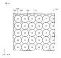
- Modification 7 In the embodiment, an example has been described in which the shape of the subpixel 10 in a plan view and the shape of the bottom surface of the lens 170 are hexagonal. In addition, in the sixth modification, an example has been described in which the shape of the subpixel 10 in a plan view and the shape of the bottom surface of the lens 170 are square or rectangular. However, the shape of the subpixel 10 in a plan view and the shape of the bottom surface of the lens 170 are not limited to these examples, and may be, for example, a circular shape or an elliptical shape as shown in FIG.
- the subpixels 10 when the subpixels 10 have a circular or elliptical shape, if adjacent subpixels 10 are brought close to each other, the adjacent subpixels 10 will contact each other at a point, as shown in FIG. 18.
- the subpixels 10 when the subpixels 10 have a hexagonal, square or rectangular shape, if adjacent subpixels 10 are brought close to each other, the subpixels 10 will contact each other at their edges, as shown in FIGS. 3A, 15A and 16A. Therefore, from the viewpoint of reducing the area of the gap between adjacent subpixels 10, it is preferable that the shape of the subpixels 10 in a planar view is hexagonal, square or rectangular. Similarly, from the viewpoint of reducing the area of the gap between adjacent lenses 170, it is preferable that the shape of the lenses 170 in a planar view is hexagonal, square or rectangular.
- the light emitting element 12 may have a resonator structure.
- “and/or” means at least one of the following, for example, "X and/or Y” means X only, Y only, or both X and Y.
- the first electrode 121 is a reflective electrode that functions as a reflective layer
- the first electrode 121 and the second electrode 123 may form a resonator structure.
- the optical distance between the first electrode 121 and the second electrode 123 may be set by the thickness of the OLED layer 122, by selecting the material of the first electrode 121, or by a combination of these.
- the first electrode 121 is a transparent electrode
- a reflective layer may be provided below the transparent electrode, and a resonator structure may be formed by the reflective layer and the second electrode 123.
- the optical distance between the reflective layer and the second electrode 123 may be set by the thickness of the OLED layer 122, by selecting the material of the reflective layer, by the thickness of an insulating layer provided between the first electrode 121 (transparent electrode) and the reflective layer, or by a combination of two or more of these.
- the display device 101 includes a plurality of light-emitting elements 12 capable of emitting white light and a color filter 16, and a combination of these elements is used to display a color image, but the colorization method of the display device 101 is not limited to this.
- the display device 101 may include a plurality of light-emitting elements capable of emitting red light, a plurality of light-emitting elements capable of emitting green light, and a plurality of light-emitting elements capable of emitting blue light, instead of the plurality of light-emitting elements 12.
- a color filter may or may not be provided.
- the above-mentioned light-emitting element is, for example, (1) a light-emitting element including a light-emitting layer capable of emitting light of a predetermined color (red light, green light, or blue light), (2) a light-emitting element including a light-emitting layer capable of emitting white light, and capable of emphasizing light of a predetermined wavelength (red light, green light, or blue light) contained in the white light emitted by the light-emitting layer by resonating it through a resonator structure, or (3) a light-emitting element including a light-emitting layer capable of emitting light of a predetermined color (red light, green light, or blue light), and capable of emphasizing light of a predetermined wavelength contained in the light of a predetermined color emitted by the light-emitting layer by resonating it through a resonator structure.
- the color filter 16 is provided has been described, but a quantum dot layer may be provided instead of the color filter 16, or a quantum dot layer may be provided together with the color filter 16.
- the quantum dot layer includes quantum dots (semiconductor particles) and can convert the color of the light emitted from the multiple light-emitting elements.
- the multiple light-emitting elements 12 may be configured to emit blue light.
- the light-emitting element 12 is an OLED element
- the light-emitting element is not limited to this example, and may be, for example, a self-luminous light-emitting element such as an LED (Light Emitting Diode) element, an inorganic electro-luminescence (IEL) element, a quantum dot light-emitting diode (QLED) element, or a semiconductor laser element.
- a self-luminous light-emitting element such as an LED (Light Emitting Diode) element, an inorganic electro-luminescence (IEL) element, a quantum dot light-emitting diode (QLED) element, or a semiconductor laser element.
- IEL inorganic electro-luminescence
- QLED quantum dot light-emitting diode
- Two or more types of light-emitting elements may be provided in the display device.
- configurations, methods, processes, shapes, materials, and values given in one embodiment are merely examples, and different configurations, methods, processes, shapes, materials, and values may be used as necessary.
- the present disclosure may also employ the following configuration.
- the lens includes a lower portion having a tapered side surface and an upper portion having a convex curved surface.
- Display device. (2) The inclination angle ⁇ of the side surface is 45° ⁇ 90°.
- the upper and lower portions are made of the same material.
- (4) The peripheral edges of the bottom surfaces of the adjacent lenses are in contact with each other in a plan view.
- the plurality of lenses have a substantially rectangular or hexagonal shape in a plan view, The sides of the bottom surfaces of the adjacent lenses are in contact with each other in a plan view.
- At least some of the lenses are shifted in an in-plane direction with respect to the light emitting element.
- the plurality of lenses are arranged such that the lens surface faces away from the light emitting element.
- the plurality of lenses are arranged so that the lens surfaces face the light-emitting element side.
- the lens further comprises a base having a curved side; The curved side surface has a gentler inclination than the lower side surface.
- (11) At least some of the lenses among the plurality of lenses have unevenness on their surfaces.
- the plurality of light-emitting elements include organic light-emitting diode elements.
- An electronic device comprising the display device according to any one of (1) to (13).
- the light-emitting portion is, for example, the light-emitting element 12 in one embodiment, etc.
- the lens member is, for example, the lens 170 in one embodiment, etc.
- the wavelength selection portion is, for example, the colored layer 160 in one embodiment, etc.
- the size of the wavelength selection section may be changed as appropriate in response to the light emitted by the light emitting section, or in the case where a light absorbing section (e.g., a black matrix section) is provided between the wavelength selection sections of adjacent light emitting sections, the size of the light absorbing section may be changed as appropriate in response to the light emitted by the light emitting section.
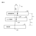
- the size of the wavelength selection section may be changed as appropriate in response to the distance (offset amount) d 0 between the normal line passing through the center of the light emitting section and the normal line passing through the center of the wavelength selection section.
- the planar shape of the wavelength selection section may be the same as, similar to, or different from the planar shape of the lens member.
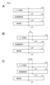
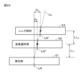
- a configuration may be adopted in which the normal line LN passing through the center of the light-emitting section 51, the normal line LN′′ passing through the center of the wavelength selecting section 52, and the normal line LN′ passing through the center of the lens member 53 do not all coincide. That is, D 0 >0, d 0 >0, and D 0 ⁇ d 0 may be satisfied.
- the center of the wavelength selecting section 52 (the position indicated by the black square in FIG. 20 ) is located on a straight line LL connecting the center of the light-emitting section 51 and the center of the lens member 53 (the position indicated by the black circle in FIG. 20 ). Specifically, when the distance in the thickness direction (vertical direction in FIG.
- the thickness direction refers to the thickness direction of the light emitting section 51 , the wavelength selecting section 52 , and the lens member 53 .
- a configuration may be adopted in which the normal line LN passing through the center of the light-emitting section 51, the normal line LN" passing through the center of the wavelength selecting section 52, and the normal line LN' passing through the center of the lens member 53 do not all coincide.
- the center of the lens member 53 (the position shown by a black circle in FIG. 22 ) is located on a straight line LL connecting the center of the light-emitting section 51 and the center of the wavelength selecting section 52 (the position shown by a black square in FIG. 22 ).
- the distance in the thickness direction vertical direction in FIG.
- the thickness direction refers to the thickness direction of the light emitting section 51 , the wavelength selecting section 52 , and the lens member 53 .
- the sub-pixel 10 included in the display device 101 may be configured to have a resonator structure that resonates light generated by the light-emitting element 12.
- the resonator structure will be described below with reference to the drawings.
- the first surface of each layer may be referred to as the upper surface.
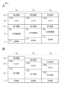
- FIG. 23A is a schematic cross-sectional view for explaining a first example of a resonator structure.
- light-emitting elements provided corresponding to the sub-pixels 10R, 10G, and 10B will be particularly distinguished.
- the light-emitting elements may be referred to as the light-emitting elements 12.
- the portions of the OLED layer 122 corresponding to the sub-pixels 10R , 10G , and 10B are referred to as the OLED layer 122R , the OLED layer 122G , and the OLED layer 122B, respectively. This is what happens.
- the first electrode 121 is formed with a common film thickness in each light-emitting element 12. The same is true for the second electrode 123.
- a reflector 71 is disposed under the first electrode 121 of the light-emitting element 12 with an optical adjustment layer 72 sandwiched therebetween.
- a resonator structure that resonates light generated by the OLED layer 122 is formed between the reflector 71 and the second electrode 123.
- the optical adjustment layers 72 provided corresponding to the sub-pixels 10R, 10G, and 10B, respectively, may be referred to as optical adjustment layers 72R , 72G , and 72B .
- the reflector 71 is formed to have a common thickness for each light-emitting element 12.
- the thickness of the optical adjustment layer 72 varies depending on the color to be displayed by the subpixel. By having the optical adjustment layers 72R , 72G , and 72B have different thicknesses, it is possible to set an optical distance that produces optimal resonance for the wavelength of light corresponding to the color to be displayed.
- the reflectors 71 of the light-emitting elements 12R , 12G , and 12B are arranged so that their upper surfaces are aligned.
- the thickness of the optical adjustment layer 72 differs depending on the color to be displayed by the subpixel, and therefore the position of the upper surface of the second electrode 123 differs depending on the type of the light-emitting element 12R , 12G , and 12B .
- the reflector 71 can be formed using metals such as aluminum (Al), silver (Ag), copper (Cu), etc., or alloys containing these as main components.
- the optical adjustment layer 72 can be made of inorganic insulating materials such as silicon nitride (SiN x ), silicon oxide (SiO x ), silicon oxynitride (SiO x N y ), or organic resin materials such as acrylic resins and polyimide resins.
- the optical adjustment layer 72 may be a single layer or a laminated film of a plurality of these materials. The number of layers may vary depending on the type of the light emitting element 12.
- the first electrode 121 can be formed using a transparent conductive material such as indium tin oxide (ITO), indium zinc oxide (IZO), or zinc oxide (ZnO).
- ITO indium tin oxide
- IZO indium zinc oxide
- ZnO zinc oxide
- the second electrode 123 must function as a semi-transmissive reflective film.
- the second electrode 123 can be formed using magnesium (Mg) or silver (Ag), or a magnesium-silver alloy (MgAg) containing these as the main components, or an alloy containing an alkali metal or an alkaline earth metal.
- FIG. 23B is a schematic cross-sectional view for explaining a second example of the resonator structure.
- the first electrode 121 and the second electrode 123 are also formed with a common film thickness in each light-emitting element 12.
- a reflector 71 is also disposed under the first electrode 121 of the light-emitting element 12, with the optical adjustment layer 72 sandwiched between them.
- a resonator structure that resonates the light generated by the OLED layer 122 is formed between the reflector 71 and the second electrode 123.
- the reflector 71 is formed with a common thickness for each light-emitting element 12, and the thickness of the optical adjustment layer 72 differs depending on the color to be displayed by the subpixel.
- the upper surfaces of the reflectors 71 in the light-emitting elements 12 R , 12 G , and 12 B are arranged so as to be aligned, and the position of the upper surface of the second electrode 123 differs depending on the type of the light-emitting element 12 R , 12 G , and 12 B.
- the upper surfaces of the second electrodes 123 are arranged to be aligned for the light-emitting elements 12R , 12G , and 12B .
- the upper surfaces of the reflectors 71 for the light-emitting elements 12R , 12G , and 12B are arranged to be different depending on the type of the light-emitting element 12R , 12G , and 12B .
- the lower surface of the reflector 71 (in other words, the upper surface of the base layer (insulating layer) 73) has a stepped shape depending on the type of the light-emitting element 12.
- the materials constituting the reflector 71, the optical adjustment layer 72, the first electrode 121, and the second electrode 123 are the same as those described in the first example, so a description thereof will be omitted.
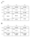
- (Resonator structure: 3rd example) 24A is a schematic cross-sectional view for explaining a third example of the resonator structure.
- the reflectors 71 provided corresponding to the sub-pixels 10R, 10G, and 10B are These reflectors are sometimes referred to as 71R , 71G , and 71B .
- the first electrode 121 and the second electrode 123 are also formed with a common film thickness in each light-emitting element 12.
- a reflector 71 is disposed under the first electrode 121 of the light-emitting element 12 with an optical adjustment layer 72 sandwiched therebetween.
- a resonator structure that resonates the light generated by the OLED layer 122 is formed between the reflector 71 and the second electrode 123.
- the film thickness of the optical adjustment layer 72 varies depending on the color to be displayed by the subpixel.
- the upper surface of the second electrode 123 is disposed so as to be aligned with the light-emitting elements 12R , 12G , and 12B .
- the bottom surface of the reflector 71 has a stepped shape according to the type of light-emitting element 12 in order to align the top surface of the second electrode 123.
- the film thickness of the reflector 71 is set to be different depending on the types of the light-emitting elements 12R , 12G , and 12B . More specifically, the film thickness is set so that the bottom surfaces of the reflectors 71R , 71G , and 71B are aligned.
- the materials constituting the reflector 71, the optical adjustment layer 72, the first electrode 121, and the second electrode 123 are the same as those described in the first example, so the description will be omitted.
- (Resonator structure: 4th example) 24B is a schematic cross-sectional view for explaining the fourth example of the resonator structure.
- the first electrodes 121 provided corresponding to the sub-pixels 10R, 10G, and 10B are , first electrodes 121R , 121G , and 121B .
- the first electrodes 121 and second electrodes 123 of each light-emitting element 12 are formed to have the same film thickness.
- a reflector 71 is disposed under the first electrodes 121 of the light-emitting elements 12 with an optical adjustment layer 72 sandwiched therebetween.
- the optical adjustment layer 72 is omitted, and the film thickness of the first electrode 121 is set to differ depending on the type of the light emitting elements 12R , 12G , and 12B .
- the reflector 71 is formed to have a common thickness for each light-emitting element 12.
- the thickness of the first electrode 121 varies depending on the color to be displayed by the subpixel. By having the first electrodes 121R , 121G , and 121B have different thicknesses, it is possible to set an optical distance that produces optimal resonance for the wavelength of light corresponding to the color to be displayed.
- the materials constituting the reflector 71, the optical adjustment layer 72, the first electrode 121, and the second electrode 123 are the same as those described in the first example, so a description thereof will be omitted.
- FIG. 25A is a schematic cross-sectional view for explaining a fifth example of the resonator structure.
- the first electrode 121 and the second electrode 123 are formed to a common thickness in each light-emitting element 12.
- a reflector 71 is disposed under the first electrode 121 of the light-emitting element 12 with an optical adjustment layer 72 sandwiched therebetween.
- the optical adjustment layer 72 is omitted, and instead, an oxide film 74 is formed on the surface of the reflector 71.
- the thickness of the oxide film 74 is set to be different depending on the type of the light-emitting elements 12R , 12G, and 12B .
- the oxide films 74 provided corresponding to the sub-pixels 10R, 10G, and 10B, respectively, may be referred to as oxide films 74R , 74G , and 74B .
- the thickness of the oxide film 74 varies depending on the color to be displayed by the sub-pixel. By having the oxide films 74R , 74G , and 74B have different thicknesses, it is possible to set an optical distance that produces optimal resonance for the wavelength of light corresponding to the color to be displayed.
- the oxide film 74 is a film formed by oxidizing the surface of the reflector 71, and is made of, for example, aluminum oxide, tantalum oxide, titanium oxide, magnesium oxide, zirconium oxide, etc.
- the oxide film 74 functions as an insulating film for adjusting the optical path length (optical distance) between the reflector 71 and the second electrode 123.
- the oxide film 74 having a thickness that varies depending on the type of the light emitting elements 12 R , 12 G , and 12 B can be formed, for example, as follows.
- the materials constituting the reflector 71, the first electrode 121, and the second electrode 123 are the same as those described in the first example, so a description thereof will be omitted.
- the light-emitting element 12 is configured by laminating a first electrode 121, an OLED layer 122, and a second electrode 123.
- the first electrode 121 is formed so as to function both as an electrode and a reflector.
- the first electrode (doubles as a reflector) 121 is formed of a material having an optical constant selected according to the type of the light-emitting elements 12R , 12G , and 12B . By varying the phase shift caused by the first electrode (doubles as a reflector) 121, it is possible to set an optical distance that generates an optimal resonance for the wavelength of light according to the color to be displayed.
- the first electrode (doubles as a reflector) 121 can be made of a single metal such as aluminum (Al), silver (Ag), gold (Au), copper (Cu), or an alloy mainly made of these metals.
- the first electrode (doubles as a reflector) 121R of the light-emitting element 12R can be made of copper (Cu)
- the first electrode (doubles as a reflector) 121G of the light-emitting element 12G and the first electrode (doubles as a reflector) 121B of the light-emitting element 12B can be made of aluminum.
- the materials constituting the second electrode 123 are the same as those described in the first example, so the description will be omitted.
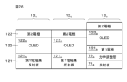
- FIG. 26 is a schematic cross-sectional view for explaining a seventh example of the resonator structure.
- the seventh example is basically a configuration in which the sixth example is applied to the light emitting elements 12 R and 12 G , and the first example is applied to the light emitting element 12 B. Even in this configuration, it is possible to set an optical distance that produces optimal resonance for the wavelength of light corresponding to the color to be displayed.
- the first electrodes (which also serve as reflectors) 121R , 121G used in the light-emitting elements 12R , 12G can be made of a single metal such as aluminum (Al), silver (Ag), gold (Au), copper (Cu), or an alloy containing these as its main component.
- the materials constituting the reflector 71B , the optical adjustment layer 72B and the first electrode 121B used in the light emitting element 12B are similar to those described in the first example, and therefore description thereof will be omitted.
- the display device 101 according to the embodiment may be provided in various electronic devices.
- the display device 101 according to the embodiment is particularly suitable for eyewear devices such as head-mounted displays, or electronic viewfinders for video cameras or single-lens reflex cameras that require high resolution and are used in a magnified state near the eyes.
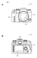
- 27A and 27B show an example of the external appearance of a digital still camera 310.
- This digital still camera 310 is a lens-interchangeable single-lens reflex type, and has an interchangeable photographing lens unit (interchangeable lens) 312 approximately in the center of the front of a camera main body (camera body) 311, and a grip part 313 for the photographer to hold on the left side of the front.
- interchangeable photographing lens unit interchangeable lens
- a monitor 314 is provided at a position shifted to the left from the center of the back of the camera body 311.
- An electronic viewfinder (eyepiece window) 315 is provided at the top of the monitor 314. By looking through the electronic viewfinder 315, the photographer can visually confirm the optical image of the subject guided by the photographing lens unit 312 and determine the composition.
- the electronic viewfinder 315 is equipped with any of the display devices 101 according to one embodiment, etc.
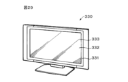
- the television device 330 has, for example, an image display screen unit 331 including a front panel 332 and a filter glass 333, and the image display screen unit 331 includes any one of the display devices 101 according to the embodiment and the like.
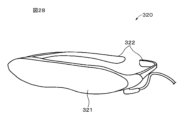
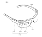
- the see-through head mounted display 340 is an example of an eyewear device.
- the see-through head mounted display 340 includes a main body 341, an arm 342, and a lens barrel 343.
- Main body 341 is connected to arm 342 and glasses 350. Specifically, the end of the long side of main body 341 is connected to arm 342, and one side of main body 341 is connected to glasses 350 via a connecting member. Note that main body 341 may also be worn directly on the head of the human body.
- Main body 341 incorporates a control board for controlling the operation of see-through head mounted display 340, and a display unit.
- Arm 342 connects main body 341 to barrel 343 and supports barrel 343. Specifically, arm 342 is coupled to an end of main body 341 and an end of barrel 343, respectively, and fixes barrel 343.
- Arm 342 also incorporates a signal line for communicating data related to images provided from main body 341 to barrel 343.
- the lens barrel 343 projects image light provided from the main body 341 via the arm 342 through the eyepiece 351 toward the eye of the user wearing the see-through head mounted display 340.
- the display unit of the main body 341 includes any one of the display devices 101 according to one embodiment.
- the smartphone 360 includes a display unit 361 that displays various information, an operation unit 362 that includes buttons that accept operation input by a user, and the like.
- the display unit 361 includes any one of the display devices 101 according to an embodiment.
- the display device 101 may be provided in various displays provided in a vehicle.
- FIGS. 32A and 32B are diagrams showing an example of the internal configuration of a vehicle 500 equipped with various displays. Specifically, FIG. 32A is a diagram showing an example of the interior of the vehicle 500 from the rear to the front, and FIG. 32B is a diagram showing an example of the interior of the vehicle 500 from diagonally rear to diagonally front.
- the vehicle 500 includes a center display 501, a console display 502, a head-up display 503, a digital rear mirror 504, a steering wheel display 505, and a rear entertainment display 506. At least one of these displays includes any of the display devices 101 according to an embodiment, etc. For example, all of these displays may include any of the display devices 101 according to an embodiment, etc.
- the center display 501 is disposed in a portion of the dashboard facing the driver's seat 508 and the passenger seat 509.
- Figs. 32A and 32B show an example of a horizontally elongated center display 501 extending from the driver's seat 508 side to the passenger seat 509 side
- the screen size and location of the center display 501 are arbitrary.
- the center display 501 can display information detected by various sensors.
- the center display 501 can display an image captured by an image sensor, an image of the distance to an obstacle in front of or beside the vehicle 500 measured by a ToF sensor, the body temperature of a passenger detected by an infrared sensor, and the like.
- the center display 501 can be used to display, for example, at least one of safety-related information, operation-related information, a life log, health-related information, authentication/identification-related information, and entertainment-related information.
- the safety-related information includes information such as detection of dozing, looking away, mischief by children in the vehicle, whether or not a seat belt is fastened, and detection of an occupant being left behind, and is information detected, for example, by a sensor arranged on the back side of the center display 501.
- the operation-related information is obtained by detecting gestures related to the operation of the occupant using a sensor.
- the detected gestures may include operations of various facilities in the vehicle 500. For example, operations of the air conditioning equipment, navigation device, AV device, lighting device, etc. are detected.
- the life log includes the life log of all occupants. For example, the life log includes a record of the actions of each occupant while on board.
- the health-related information is obtained by detecting the body temperature of the occupant using a sensor such as a temperature sensor, and inferring the health condition of the occupant based on the detected body temperature.
- a sensor such as a temperature sensor
- the face of the occupant may be captured using an image sensor, and the health condition of the occupant may be inferred from the facial expression captured in the image.
- the occupant may be spoken to by an automated voice and the occupant's health condition may be inferred based on the occupant's responses.
- Authentication/identification related information includes a keyless entry function that uses a sensor to perform face authentication, a function for automatically adjusting the seat height and position by face recognition, etc.
- Entertainment related information includes a function for detecting operation information of an AV device by an occupant using a sensor, a function for recognizing the occupant's face using a sensor and providing content suitable for the occupant via an AV device, etc.
- the console display 502 can be used, for example, to display life log information.
- the console display 502 is disposed near the shift lever 511 on the center console 510 between the driver's seat 508 and the passenger seat 509.
- the console display 502 can also display information detected by various sensors.
- the console display 502 may also display an image of the surroundings of the vehicle captured by an image sensor, or an image showing the distance to obstacles around the vehicle.
- the head-up display 503 is virtually displayed behind the windshield 512 in front of the driver's seat 508.
- the head-up display 503 can be used to display, for example, at least one of safety-related information, operation-related information, a life log, health-related information, authentication/identification-related information, and entertainment-related information. Since the head-up display 503 is often virtually positioned in front of the driver's seat 508, it is suitable for displaying information directly related to the operation of the vehicle 500, such as the speed of the vehicle 500 and the remaining fuel (battery) level.
- the digital rear-view mirror 504 can not only display the rear of the vehicle 500, but can also display the state of passengers in the back seats, so by placing a sensor on the back side of the digital rear-view mirror 504, it can be used to display life log information, for example.
- the steering wheel display 505 is disposed near the center of the steering wheel 513 of the vehicle 500.
- the steering wheel display 505 can be used to display, for example, at least one of safety-related information, operation-related information, life log, health-related information, authentication/identification-related information, and entertainment-related information.
- the steering wheel display 505 since the steering wheel display 505 is located near the driver's hands, it is suitable for displaying life log information such as the driver's body temperature, and for displaying information related to the operation of AV equipment, air conditioning equipment, etc.
- the rear entertainment display 506 is attached to the rear side of the driver's seat 508 and passenger seat 509, and is intended for viewing by rear seat passengers.
- the rear entertainment display 506 can be used to display at least one of safety-related information, operation-related information, life log, health-related information, authentication/identification-related information, and entertainment-related information, for example.
- information related to the rear seat passengers is displayed on the rear entertainment display 506.
- the rear entertainment display 506 may display information related to the operation of AV equipment or air conditioning equipment, or may display the results of measuring the body temperature of the rear seat passengers using a temperature sensor.
- a sensor may be arranged on the back side of the display device 101, etc., so that the distance to an object in the vicinity can be measured.
- Optical distance measurement methods are broadly divided into passive and active types. Passive types measure distance by receiving light from an object without projecting light from the sensor onto the object. Passive types include the lens focusing method, the stereo method, and the monocular vision method. Active types measure distance by projecting light onto an object and receiving reflected light from the object with a sensor. Active types include the optical radar method, the active stereo method, the photometric stereo method, the moire topography method, and the interference method.
- the display device 101 according to one embodiment can be applied to any of these distance measurement methods. By using a sensor arranged on the back side of the display device 101, the above-mentioned passive or active distance measurement can be performed.
Landscapes
- Physics & Mathematics (AREA)
- Optics & Photonics (AREA)
- General Physics & Mathematics (AREA)
- Engineering & Computer Science (AREA)
- Theoretical Computer Science (AREA)
- Electroluminescent Light Sources (AREA)
Abstract
光取り出し機能を向上させることができる表示装置を提供する。 表示装置は、二次元配列された複数の発光素子と、複数の発光素子それぞれに対応して設けられた複数のレンズとを備える。レンズは、テーパー状の側面を有する下部と、凸湾曲面状を有する上部とを含む。
Description
本開示は、表示装置およびそれを備える電子機器に関する。
表示装置の高輝度化および高効率化の技術として、レンズによる集光技術がある。レンズの集光効果をより有効に活用するためには、隣接するレンズ間の距離を低減することが望ましい。
例えば特許文献1には、光路制御手段として凸レンズ部材(オンチップマイクロ凸レンズ)が用いられ、隣接する凸レンズ部材同士を接する形態とすることが記載されている。
しかしながら、従来のレンズでは、隣接するレンズ間の距離を低減すると、光取り出し機能が低下する。
本開示の目的は、光取り出し機能を向上させることができる表示装置およびそれを備える電子機器を提供することにある。
上述の課題を解決するために、本開示に係る表示装置は、
二次元配列された複数の発光素子と、
複数の発光素子それぞれに対応して設けられた複数のレンズと
を備え、
レンズは、テーパー状の側面を有する下部と、凸湾曲面状を有する上部とを含む。
二次元配列された複数の発光素子と、
複数の発光素子それぞれに対応して設けられた複数のレンズと
を備え、
レンズは、テーパー状の側面を有する下部と、凸湾曲面状を有する上部とを含む。
本開示の実施形態等について以下の順序で説明する。
1 本開示に係る表示装置の全般に関する説明
2 本開示の実施形態を創作するに至る背景
3 一実施形態(表示装置の例)
4 変形例
5 発光部、レンズ部材、波長選択部のそれぞれの中心を通る法線の関係
6 共振器構造の例
7 応用例(電子機器の例)
以下に説明する実施形態等は本開示の好適な具体例であり、本開示の内容がこれらの実施形態等に限定されるものではない。なお、以下の説明において、実質的に同一の機能構成を有するものについては同一の符号を付し、重複説明を適宜省略する。また、図示が煩雑になることを防止するために、一部の構成のみに参照符号を付す場合や、図示を簡略化したり、拡大または縮小する場合もある。
1 本開示に係る表示装置の全般に関する説明
2 本開示の実施形態を創作するに至る背景
3 一実施形態(表示装置の例)
4 変形例
5 発光部、レンズ部材、波長選択部のそれぞれの中心を通る法線の関係
6 共振器構造の例
7 応用例(電子機器の例)
以下に説明する実施形態等は本開示の好適な具体例であり、本開示の内容がこれらの実施形態等に限定されるものではない。なお、以下の説明において、実質的に同一の機能構成を有するものについては同一の符号を付し、重複説明を適宜省略する。また、図示が煩雑になることを防止するために、一部の構成のみに参照符号を付す場合や、図示を簡略化したり、拡大または縮小する場合もある。
<1 本開示に係る表示装置の全般に関する説明>
本開示に係る表示装置において、レンズの下部の底面は、例えば、略円形状、略楕円形状または略多角形状を有している。複数のレンズを細密充填配列するためには、レンズの下部の底面は、略四角形状または略六角形状を有していることが好ましい。ここで、略円形状、略楕円形状または略多角形状には、厳密な意味での円形状、楕円形状または多角形状に限られず、円形状、楕円形状または多角形状に近いと視認される程度の形状が含まれる。例えば、公差や誤差等の範囲内で歪んだり変形したりした円形状、楕円形状または多角形状が含まれる。略多角形状には、具体的には例えば、多角形状の角が丸くなった形状、および多角形状の角が切り欠かされた形状が含まれる。
本開示に係る表示装置において、レンズの下部の底面は、例えば、略円形状、略楕円形状または略多角形状を有している。複数のレンズを細密充填配列するためには、レンズの下部の底面は、略四角形状または略六角形状を有していることが好ましい。ここで、略円形状、略楕円形状または略多角形状には、厳密な意味での円形状、楕円形状または多角形状に限られず、円形状、楕円形状または多角形状に近いと視認される程度の形状が含まれる。例えば、公差や誤差等の範囲内で歪んだり変形したりした円形状、楕円形状または多角形状が含まれる。略多角形状には、具体的には例えば、多角形状の角が丸くなった形状、および多角形状の角が切り欠かされた形状が含まれる。
本開示において、テーパー状とは、レンズの下部の高さに対して径が線形に変わり、下部の側面の傾斜角度が一定になる厳密な意味での線形テーパー状に限られず、線形テーパー状に近いと視認される程度の形状が含まれる。例えば、公差や誤差等の範囲内で歪んだり変形したりした線形テーパー状が含まれる。
本開示において、テーパー状の側面は、例えば、略円錐台面状、略楕円錐台面状または略多角錐台面状を有する。複数のレンズを細密充填配列するためには、テーパー状の側面は、略四角錐台面状または略六角錐台面状を有することが好ましい。ここで、略円錐台面状、略楕円錐台面状または略多角錐台面状には、厳密な意味での円錐台面状、楕円錐台面状または多角錐台面状に限られず、円錐台面状、楕円錐台面状または多角錐台面状に近いと視認される程度の形状が含まれる。例えば、公差や誤差等の範囲内で歪んだり変形したりした円錐台面状、楕円錐台面状または多角錐台面状が含まれる。略多角錐台面状には、具体的には例えば、多角錐台面状の側稜が丸くなった形状、および多角錐台面状の側稜が切り欠かされた形状が含まれる。
本開示において、「対象物Bが対象物A上に設けられている」等の表現にて「対象物A上」とは、対象物Aと対象物Bとの相対的な位置関係を示すものであり、対象物Bが他の対象物を間に挟まずに直接対象物Aの上に位置している状態のみならず、対象物Bが少なくとも1つの他の対象物を間に挟んで対象物Aの上に位置している状態も含む概念である。
本開示に係る表示装置は、電子機器に備えられてもよい。例えば、本開示に係る表示装置は、VR(Virtual Reality)装置、MR(Mixed Reality)装置またはAR(Augmented Reality)装置等のアイウェアデバイスに備えられてもよいし、電子ビューファインダ(Electronic View Finder:EVF)または小型プロジェクタ等に備えられてもよい。
<2 本開示の実施形態を創作するに至る背景>
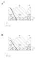
図1Aに示されるように、隣接するレンズ41間の距離が大きいと、発光素子12から出射された光Lが、レンズ41間の平坦部から漏れ易くなる。このような光漏れを抑制し、レンズ41の集光効果をより有効に活用するためには、隣接するレンズ41間の距離を低減することが望ましい。
図1Aに示されるように、隣接するレンズ41間の距離が大きいと、発光素子12から出射された光Lが、レンズ41間の平坦部から漏れ易くなる。このような光漏れを抑制し、レンズ41の集光効果をより有効に活用するためには、隣接するレンズ41間の距離を低減することが望ましい。
しかしながら、凸湾曲面状を有するレンズ41では、隣接するレンズ41間の距離を低減すると、図1Bに示されるように、隣接するレンズ41の下部側面同士が接近し、隣接するレンズ41の一方の下部から他方の下部に光Lが漏れ出しやすくなる。したがって、レンズ41の下部のレンズとしての機能が低下し、レンズ41の光取り出し機能が低下する。
本発明者らは、上記の知見に基づき、隣接するレンズ間の距離を低減した場合にも、レンズ41の光取り出し機能の低下を抑制できるレンズについて鋭意検討を行った。その結果、上部が凸湾曲面状であり、下部がテーパー状の側面であるレンズを見出すに至った。
<3 一実施形態>
[表示装置101の概略構成]
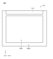
図2は、一実施形態に係る表示装置101の平面図である。表示装置101は、有効画素領域RE1と、有効画素領域RE1の周辺に設けられた周辺領域RE2とを有する。表示装置101は、OLED(Organic Light Emitting Diode)表示装置であってもよい。本明細書において、表示装置101の表示面内において直行する第1方向および第2方向をそれぞれ、X軸方向およびY軸方向といい、表示装置101の表示面に対して垂直な方向をZ軸方向という。一実施形態においては、X軸方向が表示面の水平方向であり、Y軸方向が表示面の垂直方向である例について説明する。
[表示装置101の概略構成]
図2は、一実施形態に係る表示装置101の平面図である。表示装置101は、有効画素領域RE1と、有効画素領域RE1の周辺に設けられた周辺領域RE2とを有する。表示装置101は、OLED(Organic Light Emitting Diode)表示装置であってもよい。本明細書において、表示装置101の表示面内において直行する第1方向および第2方向をそれぞれ、X軸方向およびY軸方向といい、表示装置101の表示面に対して垂直な方向をZ軸方向という。一実施形態においては、X軸方向が表示面の水平方向であり、Y軸方向が表示面の垂直方向である例について説明する。
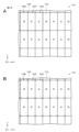
図3Aは、有効画素領域RE1の一部を拡大して表す平面図である。複数の副画素10R、複数の副画素10Gおよび複数の副画素10Bが、有効画素領域RE1に設けられている。以下の説明において、副画素10R、10G、10Bを特に区別せず総称する場合には、副画素10R、10G、10Bを単に副画素10ということがある。複数の副画素10は、規定の配列パターンで2次元配列されている。一実施形態では、複数の副画素10の配列パターンがデルタ配列である例について説明する。パッド部113および映像表示用のドライバ(図示せず)等が、周辺領域RE2に設けられている。図示しないフレキシブルプリント配線基板(Flexible Printed Circuit:FPC)が、パッド部113に接続されてもよい。
副画素10R、10G、10Bは、互いに異なる色の光を出射することができる。副画素10Rは、赤色光を出射することができる。副画素10Gは、緑色光を出射することができる。副画素10Bは、青色光を出射することができる。図3A中にて文字「R」、「G」、「B」が付された区画はそれぞれ、副画素10R、副画素10G、副画素10Bを表している。
1画素10Pが、隣接する3つの副画素10R、10G、10Bにより構成されていてもよい。但し、1画素10Pの構成はこの例に限定されるものではない。副画素10は、図3Aに示されるように、平面視において六角形状を有していてもよいし、図3Bに示されるように、六角形状の角が丸くなった形状を有していてもよい。図3Aおよび図3Bでは副画素10R、10G、10Bの輪郭を図示しているが、隣接する副画素10R、10G、10B間に、明確な境界があるとは限らない。
[表示装置101の層構成]
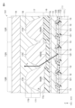
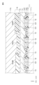
図4は、図3のIV-IV線に沿った断面図である。表示装置101は、駆動基板11と、複数の発光素子12と、絶縁層13と、保護層14と、平坦化層15と、カラーフィルタ16と、レンズアレイ17と、充填樹脂層18と、基板19とを備える。
図4は、図3のIV-IV線に沿った断面図である。表示装置101は、駆動基板11と、複数の発光素子12と、絶縁層13と、保護層14と、平坦化層15と、カラーフィルタ16と、レンズアレイ17と、充填樹脂層18と、基板19とを備える。
本明細書において、表示装置101を構成する各層の両面のうち、表示装置101の表示面側(トップ側)となる面を第1面(上面)といい、表示装置101の表示面とは反対側(ボトム側)となる面を第2面(下面)ということがある。本明細書において、平面視とは、第1面に垂直な方向から対象物が見られたときの平面視を意味する。
(駆動基板11)
駆動基板11は、いわゆるバックプレーンであり、複数の発光素子12を駆動することができる。駆動基板11は、例えば、基板111と、絶縁層112とを順に備える。
駆動基板11は、いわゆるバックプレーンであり、複数の発光素子12を駆動することができる。駆動基板11は、例えば、基板111と、絶縁層112とを順に備える。
複数の駆動回路(図示せず)および複数の配線(図示せず)等が、基板111の第1面側に設けられている。基板111は、例えば、トランジスタ等の形成が容易な半導体基板であってもよいし、水分および酸素の透過性が低いガラス基板または樹脂基板であってもよい。半導体基板は、例えば、アモルファスシリコン、多結晶シリコンまたは単結晶シリコン等を含む。ガラス基板は、例えば、高歪点ガラス、ソーダガラス、ホウケイ酸ガラス、フォルステライト、鉛ガラスまたは石英ガラス等を含む。樹脂基板は、例えば、ポリメチルメタクリレート、ポリビニルアルコール、ポリビニルフェノール、ポリエーテルスルホン、ポリイミド、ポリカーボネート、ポリエチレンテレフタラートおよびポリエチレンナフタレート等からなる群より選ばれた少なくとも1種を含む。
絶縁層112は、基板111の第1面上に設けられ、複数の駆動回路および複数の配線等を覆っている。複数の配線は、パッド部113に接続されていてもよい。絶縁層112は、複数のコンタクト部(図示せず)を内部に備える。複数のコンタクト部は、発光素子12と駆動回路または配線とを電気的に接続する。コンタクト部は、例えば、銅(Cu)およびチタン(Ti)等からなる群より選ばれた少なくとも1種の金属を含む。
絶縁層112は、有機絶縁層であってもよいし、無機絶縁層であってもよいし、これらの積層体であってもよい。有機絶縁層は、例えば、ポリイミド系樹脂、アクリル系樹脂およびノボラック系樹脂等からなる群より選ばれた少なくとも1種を含む。無機絶縁層は、例えば、酸化シリコン(SiOx)、窒化シリコン(SiNx)および酸窒化シリコン(SiOxNy)等からなる群より選ばれた少なくとも1種を含む。
(発光素子12)
発光素子12は、駆動回路等の制御に基づき、白色光を発光することができる。発光素子12は、有機発光ダイオード素子(OLED素子)であってもよい。発光素子12は、各色の副画素10R、10G、10Bに含まれる。
発光素子12は、駆動回路等の制御に基づき、白色光を発光することができる。発光素子12は、有機発光ダイオード素子(OLED素子)であってもよい。発光素子12は、各色の副画素10R、10G、10Bに含まれる。
複数の発光素子12は、規定の配置パターンで駆動基板11の第1面上に2次元配置されている。規定の配置パターンは、複数の副画素10の規定の配置パターンとして説明したとおりである。発光素子12は、第1電極121と、OLED層122と、第2電極123とを駆動基板11の第1面上に順に備える。
(第1電極121)
第1電極121は、OLED層122の第2面側に設けられている。第1電極121は、有効画素領域RE1内において複数の発光素子12で個別に設けられている個別電極である。すなわち、第1電極121は、有効画素領域RE1内において、駆動基板11の第1面の面内方向に隣接する発光素子12の間で分断されている。第1電極121は、アノードである。第1電極121と第2電極123の間に電圧が加えられると、第1電極121からOLED層122にホールが注入される。
第1電極121は、OLED層122の第2面側に設けられている。第1電極121は、有効画素領域RE1内において複数の発光素子12で個別に設けられている個別電極である。すなわち、第1電極121は、有効画素領域RE1内において、駆動基板11の第1面の面内方向に隣接する発光素子12の間で分断されている。第1電極121は、アノードである。第1電極121と第2電極123の間に電圧が加えられると、第1電極121からOLED層122にホールが注入される。
第1電極121は、例えば、金属層により構成されてもよいし、金属層と透明導電性酸化物層により構成されてもよい。第1電極121が金属層と透明導電性酸化物層により構成されている場合には、高い仕事関数を有する層をOLED層122に隣接させる観点からすると、透明導電性酸化物層がOLED層122側に設けられることが好ましい。
金属層は、OLED層122で発光された光を反射する反射層としての機能を有していてもよい。金属層は、例えば、クロム(Cr)、金(Au)、白金(Pt)、ニッケル(Ni)、銅(Cu)、モリブデン(Mo)、チタン(Ti)、タンタル(Ta)、アルミニウム(Al)、マグネシウム(Mg)、鉄(Fe)、タングステン(W)および銀(Ag)からなる群より選ばれた少なくとも1種の金属元素を含む。金属層は、上記少なくとも1種の金属元素を合金の構成元素として含んでいてもよい。合金の具体例としては、アルミニウム合金または銀合金が挙げられる。アルミニウム合金の具体例としては、例えば、AlNdまたはAlCuが挙げられる。
下地層(図示せず)が、金属層の第2面側に隣接して設けられていてもよい。下地層は、金属層の成膜時に、金属層の結晶配向性を向上させることができてもよい。下地層は、例えば、チタン(Ti)およびタンタル(Ta)からなる群より選ばれた少なくとも1種の金属元素を含む。下地層は、上記少なくとも1種の金属元素を合金の構成元素として含んでいてもよい。
透明導電性酸化物層は、透明導電性酸化物を含む。透明導電性酸化物は、例えば、インジウムを含む透明導電性酸化物(以下「インジウム系透明導電性酸化物」という。)、錫を含む透明導電性酸化物(以下「錫系透明導電性酸化物」という。)および亜鉛を含む透明導電性酸化物(以下「亜鉛系透明導電性酸化物」という。)からなる群より選ばれた少なくとも1種を含む。
インジウム系透明導電性酸化物は、例えば、酸化インジウム錫(ITO)、酸化インジウム亜鉛(IZO)、酸化インジウムガリウム(IGO)、酸化インジウムガリウム亜鉛(IGZO)またはフッ素ドープ酸化インジウム(IFO)を含む。これらの透明導電性酸化物のうちでも酸化インジウム錫(ITO)が特に好ましい。酸化インジウム錫(ITO)は、仕事関数的にOLED層122へのホール注入障壁が特に低いため、表示装置101の駆動電圧を特に低電圧化することができるからである。錫系透明導電性酸化物は、例えば、酸化錫、アンチモンドープ酸化錫(ATO)またはフッ素ドープ酸化錫(FTO)を含む。亜鉛系透明導電性酸化物は、例えば、酸化亜鉛、アルミニウムドープ酸化亜鉛(AZO)、ホウ素ドープ酸化亜鉛またはガリウムドープ酸化亜鉛(GZO)を含む。
(OLED層122)
OLED層122は、白色光を発光することができる。OLED層122は、複数の第1電極121と1つの第2電極123の間に設けられている。OLED層122は、有効画素領域RE1内において、駆動基板11の第1面の面内方向に隣接する発光素子12間で繋がり、有効画素領域RE1内において複数の発光素子12で共通の層である。
OLED層122は、白色光を発光することができる。OLED層122は、複数の第1電極121と1つの第2電極123の間に設けられている。OLED層122は、有効画素領域RE1内において、駆動基板11の第1面の面内方向に隣接する発光素子12間で繋がり、有効画素領域RE1内において複数の発光素子12で共通の層である。
OLED層122は、有機発光層を含む積層体により構成されてもよく、その場合、積層体のうちの一部の層(例えば電子注入層)は無機層であってもよい。OLED層122は、単層の発光ユニットを備えるOLED層であってもよいし、2層の発光ユニットを備えるOLED層(タンデム構造)であってもよいし、これら以外の構造のOLED層であってもよい。単層の発光ユニットを備えるOLED層は、例えば、第1電極121から第2電極123に向かって、正孔注入層、正孔輸送層、赤色発光層、発光分離層、青色発光層、緑色発光層、電子輸送層、電子注入層がこの順序で積層された構成を有する。2層の発光ユニットを備えるOLED層は、例えば、第1電極121から第2電極123に向かって、正孔注入層、正孔輸送層、青色発光層、電子輸送層、電荷発生層、正孔輸送層、黄色発光層、電子輸送層と、電子注入層がこの順序で積層された構成を有する。
正孔注入層は、各発光層への正孔注入効率を高めると共に、リークを抑制することができる。正孔輸送層は、各発光層への正孔輸送効率を高めることができる。電子注入層は、各発光層への電子注入効率を高めることができる。電子輸送層は、各発光層への電子輸送効率を高めることができる。発光分離層は、各発光層へのキャリアの注入を調整するための層であり、発光分離層を介して各発光層に電子やホールが注入されることにより各色の発光バランスが調整される。電荷発生層は、当該電荷発生層を挟むように設けられた2つの発光層に電子と正孔をそれぞれ供給することができる。
赤色発光層、緑色発光層、青色発光層、黄色発光層はそれぞれ、電界をかけることにより、第1電極121または電荷発生層から注入された正孔と第2電極123または電荷発生層から注入された電子との再結合が起こり、赤色光、緑色光、青色光、黄色光を発光することができる。
(第2電極123)
第2電極123は、OLED層122の第1面側に設けられている。第2電極123は、有効画素領域RE1内において、駆動基板11の第1面の面内方向に隣接する発光素子12間で繋がり、有効画素領域RE1内において複数の発光素子12で共通の電極である。
第2電極123は、OLED層122の第1面側に設けられている。第2電極123は、有効画素領域RE1内において、駆動基板11の第1面の面内方向に隣接する発光素子12間で繋がり、有効画素領域RE1内において複数の発光素子12で共通の電極である。
第2電極123は、カソードである。第1電極121と第2電極123の間に電圧が加えられると、第2電極123からOLED層122に電子が注入される。第2電極123は、OLED層122から発せられる白色光に対して透光性を有している。第2電極123は、可視光に対して透明性を有する透明電極であることが好ましい。本明細書において、可視光とは、360nm以上830nmの波長域の光をいう。
第2電極123は、できるだけ透光性が高く、かつ仕事関数が小さい材料によって構成されることが、発光効率を高める上で好ましい。第2電極123は、例えば、金属層および透明導電性酸化物層のうちの少なくとも一層により構成されている。より具体的には、第2電極123は、金属層もしくは透明導電性酸化物層の単層膜、または金属層と透明導電性酸化物層の積層膜により構成されている。第2電極123が積層膜により構成されている場合、金属層がOLED層122側に設けられてもよいし、透明導電性酸化物層がOLED層122側に設けられてもよいが、低い仕事関数を有する層をOLED層122に隣接させる観点からすると、金属層がOLED層122側に設けられていることが好ましい。
金属層は、例えば、マグネシウム(Mg)、アルミニウム(Al)、銀(Ag)、カルシウム(Ca)およびナトリウム(Na)からなる群より選ばれた少なくとも1種の金属元素を含む。金属層は、上記少なくとも1種の金属元素を合金の構成元素として含んでいてもよい。合金の具体例としては、MgAg合金、MgAl合金またはAlLi合金等が挙げられる。透明導電性酸化物層は、透明導電性酸化物を含む。当該透明導電性酸化物としては、上記の第1電極121の透明導電性酸化物と同様の材料を例示することができる。
(絶縁層13)
絶縁層13は、駆動基板11の第1面のうち、離隔された第1電極121の間の部分に設けられている。絶縁層13は、駆動基板11の第1面の面内方向に隣接する第1電極121の間を絶縁することができる。絶縁層13は、複数の開口131を有する。複数の開口131はそれぞれ、各発光素子12に対応して設けられている。複数の開口131がそれぞれ、各第1電極121の第1面(OLED層122側の面)上に設けられていてもよい。開口131を介して、第1電極121とOLED層122とが接触する。
絶縁層13は、駆動基板11の第1面のうち、離隔された第1電極121の間の部分に設けられている。絶縁層13は、駆動基板11の第1面の面内方向に隣接する第1電極121の間を絶縁することができる。絶縁層13は、複数の開口131を有する。複数の開口131はそれぞれ、各発光素子12に対応して設けられている。複数の開口131がそれぞれ、各第1電極121の第1面(OLED層122側の面)上に設けられていてもよい。開口131を介して、第1電極121とOLED層122とが接触する。
絶縁層13は、有機絶縁層であってもよいし、無機絶縁層であってもよいし、これらの積層体であってもよい。有機絶縁層は、例えば、ポリイミド系樹脂、アクリル系樹脂およびノボラック系樹脂等からなる群より選ばれた少なくとも1種を含む。無機絶縁層は、例えば、酸化シリコン(SiOx)、窒化シリコン(SiNx)および酸窒化シリコン(SiOxNy)等からなる群より選ばれた少なくとも1種を含む。
(保護層14)
保護層14は、第2電極123の第1面上に設けられ、複数の発光素子12を覆っている。保護層14は、発光素子12から発せられる白色光に対して透光性を有している。保護層14は、複数の発光素子12等を保護することができる。例えば、保護層14は、外部環境から複数の発光素子12等への水分浸入を抑制することができる。また、第2電極123が金属層により構成されている場合には、保護層14は、この金属層の酸化を抑制する機能を有していてもよい。
保護層14は、第2電極123の第1面上に設けられ、複数の発光素子12を覆っている。保護層14は、発光素子12から発せられる白色光に対して透光性を有している。保護層14は、複数の発光素子12等を保護することができる。例えば、保護層14は、外部環境から複数の発光素子12等への水分浸入を抑制することができる。また、第2電極123が金属層により構成されている場合には、保護層14は、この金属層の酸化を抑制する機能を有していてもよい。
保護層14は、例えば、吸湿性が低い無機材料および有機材料の少なくとも一方を含む。保護層14は、単層構造であってもよいし、多層構造であってもよい。保護層14の厚さを厚くする場合には、多層構造とすることが好ましい。保護層14における内部応力を緩和するためである。無機材料は、例えば、酸化シリコン(SiOx)、窒化シリコン(SiNx)、酸化窒化シリコン(SiOxNy)、酸化チタン(TiOx)および酸化アルミニウム(AlOx)等からなる群より選ばれた少なくとも1種を含む。有機材料は、例えば、熱硬化性樹脂および感光性樹脂等からなる群より選ばれた少なくとも1種の樹脂の硬化物を含む。感光性樹脂は、例えば、紫外線硬化性樹脂を含む。有機材料は、具体的には例えば、アクリル系樹脂、ポリイミド系樹脂、ノボラック系樹脂、エポキシ系樹脂、ノルボルネン系樹脂およびパリレン系樹脂等からなる群より選ばれた少なくとも1種を含む。
保護層14は、原子層が堆積された堆積層を含むことが好ましい。堆積層は、ALD(Atomic Layer Deposition)層であってもよい。保護層14が堆積層を含むことにより、保護層14による水分浸入の抑制効果を向上させることができる。堆積層は、例えば、金属酸化物または金属窒化物を含む。金属酸化物は、例えば、酸化アルミニウム(AlOx)または酸化チタン(TiOx)を含む。金属窒化物は、例えば、窒化チタン(TiNx)を含む。
(平坦化層15)
平坦化層15は、保護層14の第1面上に設けられている。平坦化層15は、保護層14の第1面の凹凸を埋め、平坦な第1面を保護層14の上側に形成することができる。平坦化層15は、発光素子12から発せられる白色光に対して透光性を有している。平坦化層15は、例えば、有機材料および無機材料の少なくとも一方を含む。
平坦化層15は、保護層14の第1面上に設けられている。平坦化層15は、保護層14の第1面の凹凸を埋め、平坦な第1面を保護層14の上側に形成することができる。平坦化層15は、発光素子12から発せられる白色光に対して透光性を有している。平坦化層15は、例えば、有機材料および無機材料の少なくとも一方を含む。
有機材料は、例えば、感光性樹脂組成物の硬化物を含む。感光性樹脂組成物は、ポジ型の感光性樹脂組成物およびネガ型の感光性樹脂組成物のいずれを含んでもよい。感光性樹脂組成物は、具体的には例えば、ポリイミド、ポリイミド前駆体、ポリベンゾオキサゾール、ポリベンゾオキサゾール前駆体、アクリル系樹脂、フェノール系樹脂およびシロキサン系樹脂等からなる群より選ばれた少なくとも1種を含む。無機材料としては、保護層14の無機材料と同様の材料を例示することができる。
(カラーフィルタ16)
カラーフィルタ16は、いわゆるオンチップカラーフィルタ(On Chip Color Filter:OCCF)である。カラーフィルタ16は、複数の発光素子12の上方に設けられている。より具体的には、カラーフィルタ16は、有効画素領域RE1における平坦化層15の第1面上に設けられている。カラーフィルタ16は、例えば、複数の着色層160Rと、複数の着色層160Gと、複数の着色層160Bとを含む。なお、以下の説明において、着色層160R、着色層160G、着色層160Bを特に区別せず総称する場合には、着色層160R、着色層160G、着色層160Bを単に着色層160ということがある。
カラーフィルタ16は、いわゆるオンチップカラーフィルタ(On Chip Color Filter:OCCF)である。カラーフィルタ16は、複数の発光素子12の上方に設けられている。より具体的には、カラーフィルタ16は、有効画素領域RE1における平坦化層15の第1面上に設けられている。カラーフィルタ16は、例えば、複数の着色層160Rと、複数の着色層160Gと、複数の着色層160Bとを含む。なお、以下の説明において、着色層160R、着色層160G、着色層160Bを特に区別せず総称する場合には、着色層160R、着色層160G、着色層160Bを単に着色層160ということがある。
複数の着色層160は、規定の配置パターンで平坦化層15の第1面上に2次元配置されている。規定の配置パターンは、複数の副画素10の規定の配置パターンとして説明したとおりである。各着色層160は、発光素子12の上方に設けられている。副画素10Rは、発光素子12と当該発光素子12の上方に設けられた着色層160Rとにより構成される。副画素10Gは、発光素子12と当該発光素子12の上方に設けられた着色層160Gとにより構成される。副画素10Bは、発光素子12と当該発光素子12の上方に設けられた着色層160Bとにより構成される。
着色層160Rは、赤色を有する。着色層160Rは、発光素子12から出射された白色光のうち赤色光の成分を透過するのに対して、赤色光以外の可視光成分を吸収することができる。着色層160Gは、緑色を有する。着色層160Gは、発光素子12から出射された白色光のうち緑色光の成分を透過するのに対して、緑色光以外の可視光成分を吸収することができる。着色層160Bは、青色を有する。着色層160Bは、発光素子12から出射された白色光のうち青色光の成分を透過するのに対して、青色光以外の可視光成分を吸収することができる。
着色層160Rは、例えば、赤色のカラーレジストを含む。着色層160Gは、例えば、緑色のカラーレジストを含む。着色層160Bは、例えば、青色のカラーレジストを含む。
(レンズアレイ17)
レンズアレイ17は、カラーフィルタ16の第1面上に設けられている。レンズアレイ17は、複数のレンズ170を含む。レンズアレイ17は、ベース層17aをさらに含んでもよい。レンズ170は、発光素子12から上方に出射された光を正面方向に集光することができる。複数のレンズ170は、いわゆるオンチップマイクロレンズ(On Chip Microlens:OCL)であり、規定の配置パターンでカラーフィルタ16の第1面上に2次元配置されている。規定の配置パターンは、複数の副画素10の規定の配置パターンとして説明したとおりである。
レンズアレイ17は、カラーフィルタ16の第1面上に設けられている。レンズアレイ17は、複数のレンズ170を含む。レンズアレイ17は、ベース層17aをさらに含んでもよい。レンズ170は、発光素子12から上方に出射された光を正面方向に集光することができる。複数のレンズ170は、いわゆるオンチップマイクロレンズ(On Chip Microlens:OCL)であり、規定の配置パターンでカラーフィルタ16の第1面上に2次元配置されている。規定の配置パターンは、複数の副画素10の規定の配置パターンとして説明したとおりである。
複数のレンズ170は、レンズ面が発光素子12側とは反対側となるように配置されている。1つのレンズ170が、1つの発光素子12の上方に設けられている。レンズ170は、下部171と、下部171上に設けられた上部172とを含む。
レンズ170の下部171は、テーパー状の側面を有する。当該テーパー状の側面は、レンズ170の頂部に向かって先細りになっている。下部171の側面の傾斜角θの下限値は、集光効果の低下を抑制する観点から、45°<θであることが好ましい。下部171の側面の傾斜角θの上限値は、例えば、θ<90°、θ<86°、θ<82°またはθ<80°である。下部171の側面の傾斜角θの数値範囲は、上記上限値と上記下限値のいずれかとにより規定されてよく、例えば、45°<θ<90°、45°<θ<86°、45°<θ<82°、45°<θ<80°である。
下部171の側面の傾斜角θは以下のようにして求められる。まず、クライオFIB(Focused Ion Beam)加工等により表示装置101の断面(表示装置101の厚さ方向に平行な断面)を切り出し、薄片を作製する。この際、レンズ170の中心軸を含むように断面は切り出される。続いて、作製した薄片をTEM(Transmission Electron Microscope)により観察し、断面TEM像を取得する。次に、取得した断面TEM像中において、下部171の側面の傾斜角θを測定する。
下部171の底面、すなわちレンズ170の底面は、図3Aに示されるように、平面視において六角形状を有していることが好ましい。下部171の底面が、図3Bに示されるように、六角形状の角が丸くなった形状を有していてもよい。下部171の底面が六角形状または六角形状の角が丸くなった形状を有することで、下部171の底面が円形状を有する場合(図18参照)に比べて、隣接するレンズ170間の隙間の面積を低減することができる。テーパー状の側面は、略六角錐台面状を有することが好ましい。
図3Aでは、平面視におけるレンズ170の底面形状と副画素10の形状が同一であり、かつ、レンズ170の底面と副画素10のサイズが同一である例が示されている。但し、レンズ170の底面形状と副画素10の形状が異なっていてもよいし、レンズ170の底面と副画素10のサイズが異なっていてもよい。
隣接するレンズ170の底面の辺同士(周縁同士)が、平面視において接していることが好ましい。これにより、隣接するレンズ170間の隙間を低減することができる。したがって、隣接するレンズ170間の隙間からの光漏れを抑制することができる。
上部172は、テーパー状の下部171の幅の狭くなっている側に設けられている。上部172は、凸湾曲面状を有する。凸湾曲面状としては、例えば、略放物面状、略半球面状または略半楕円面状等が挙げられるが、これらの形状に限定されるものではない。ここで、略放物面状、略半球面状または略半楕円面状には、厳密な意味での放物面状、半球面状または半楕円面状に限られず、放物面状、半球面状または半楕円面状に近いと視認される程度の形状が含まれる。例えば、公差や誤差等の範囲内で歪んだり変形したりした放物面状、半球面状または半楕円面状が含まれる。上部172と下部171は、滑らかに繋がっていることが好ましい。
レンズ170の屈折率n1、すなわち下部171および上部172の屈折率は、充填樹脂層18の屈折率n2に比べて大きいことが好ましい。レンズ170の屈折率n1が充填樹脂層18の屈折率n2に比べて大きいことで、下部171のテーパー面および上部172の凸状曲面にて光を屈折させ正面方向に立ち上げることができる。したがって、光取り出し機能を向上させることができる。なお、本開示において、屈折率n1、n2は、波長589.3nmの光(ナトリウムのD線)に対する屈折率を表す。
下部171および上部172は、例えば、異なる材料または同一材料、好ましくは、同一材料により構成されている。下部171および上部172が同一材料により構成されていることで、表示装置101の製造に必要な材料の種類を減らすことができる。したがって、表示装置101の生産性を向上し、かつ、表示装置101の製造コストを低減することができる。また、下部171および上部172が同一材料により構成されていることで、下部171と上部172の屈折率が揃うため、下部171と上部172の間の界面における反射を抑制することもできる。
下部171および上部172は、例えば、可視光に対して透明な無機材料または高分子樹脂を含む。無機材料は、例えば、酸化シリコン(SiOx)を含む。高分子樹脂は、例えば、紫外線硬化樹脂等の感光性樹脂を含む。
ベース層17aは、複数のレンズ170とカラーフィルタ16との間に設けられている。ベース層17aは、例えば、レンズ170の下部171と同一の材料により構成されている。なお、ベース層17aは、必要に応じて設けられるものであり、設けられていてもよいし、設けられていなくてもよい。
(充填樹脂層18)
充填樹脂層18は、レンズアレイ17の第1面上に設けられ、レンズアレイ17と基板19の間の空間に充填されている。充填樹脂層18は、カラーフィルタ16から出射される各色の光に対して透光性を有している。充填樹脂層18は、レンズアレイ17と基板19を接着する接着層としての機能を有していることが好ましい。
充填樹脂層18は、レンズアレイ17の第1面上に設けられ、レンズアレイ17と基板19の間の空間に充填されている。充填樹脂層18は、カラーフィルタ16から出射される各色の光に対して透光性を有している。充填樹脂層18は、レンズアレイ17と基板19を接着する接着層としての機能を有していることが好ましい。
充填樹脂層18は、例えば、硬化性樹脂の硬化物を含む。硬化性樹脂は、例えば、熱硬化性樹脂および紫外線硬化性樹脂等からなる群より選ばれた少なくとも1種を含む。なお、充填樹脂層18は、熱硬化性樹脂および紫外線硬化性樹脂に限定されるものではなく、熱硬化性樹脂および紫外線硬化性樹脂以外の種類の硬化性樹脂を含んでもよい。
(基板19)
基板19は、充填樹脂層18の第1面上に設けられている。基板19は、複数の発光素子12等が設けられた駆動基板11の第1面を封止する。基板19は、カラーフィルタ16から出射される各色の光に対して透光性を有している。基板19は、例えば、ガラス基板である。
基板19は、充填樹脂層18の第1面上に設けられている。基板19は、複数の発光素子12等が設けられた駆動基板11の第1面を封止する。基板19は、カラーフィルタ16から出射される各色の光に対して透光性を有している。基板19は、例えば、ガラス基板である。
[表示装置101の製造方法]
以下、図5から図9を参照して、一実施形態に係る表示装置101の製造方法の一例について説明する。
以下、図5から図9を参照して、一実施形態に係る表示装置101の製造方法の一例について説明する。
(第1電極121の形成工程)
まず、例えばスパッタリング法により、金属層、金属酸化物層を駆動基板11の第1面上に順次形成した後、例えばフォトリソグラフィ技術を用いて金属層および金属酸化物層をパターニングする。これにより、複数の第1電極121が駆動基板11の第1面上に形成される。
まず、例えばスパッタリング法により、金属層、金属酸化物層を駆動基板11の第1面上に順次形成した後、例えばフォトリソグラフィ技術を用いて金属層および金属酸化物層をパターニングする。これにより、複数の第1電極121が駆動基板11の第1面上に形成される。
(絶縁層13の形成工程)
次に、例えばCVD(Chemical Vapor Deposition)法により、複数の第1電極121を覆うように駆動基板11の第1面上に絶縁層13を形成する。次に、例えばフォトリソグラフィ技術により、絶縁層13を加工することにより、各第1電極121の第1面上に開口131を形成する。
次に、例えばCVD(Chemical Vapor Deposition)法により、複数の第1電極121を覆うように駆動基板11の第1面上に絶縁層13を形成する。次に、例えばフォトリソグラフィ技術により、絶縁層13を加工することにより、各第1電極121の第1面上に開口131を形成する。
(OLED層122の形成工程)
次に、例えば蒸着法により、正孔輸送層、赤色発光層、発光分離層、青色発光層、緑色発光層、電子輸送層、電子注入層を複数の第1電極121の第1面上および絶縁層13の第1面上にこの順序で積層する。これにより、OLED層122が形成される。
次に、例えば蒸着法により、正孔輸送層、赤色発光層、発光分離層、青色発光層、緑色発光層、電子輸送層、電子注入層を複数の第1電極121の第1面上および絶縁層13の第1面上にこの順序で積層する。これにより、OLED層122が形成される。
(第2電極123の形成工程)
次に、例えば蒸着法またはスパッタリング法により、第2電極123をOLED層122の第1面上に形成する。これにより、駆動基板11の第1面上に複数の発光素子12が形成される。
次に、例えば蒸着法またはスパッタリング法により、第2電極123をOLED層122の第1面上に形成する。これにより、駆動基板11の第1面上に複数の発光素子12が形成される。
(保護層14の形成工程)
次に、例えばCVD法または蒸着法により、保護層14を第2電極123の第1面上に形成する。
次に、例えばCVD法または蒸着法により、保護層14を第2電極123の第1面上に形成する。
(平坦化層15の形成工程)
次に、樹脂組成物を保護層14の第1面上に塗布した後、例えば光照射または加熱により硬化させることにより、平坦化層15を形成する。
次に、樹脂組成物を保護層14の第1面上に塗布した後、例えば光照射または加熱により硬化させることにより、平坦化層15を形成する。
(カラーフィルタ16の形成工程)
次に、平坦化層15の第1面上に緑色のカラーレジストを塗布し、フォトマスクを介して紫外線を照射しパターン露光した後、現像することにより、緑色の着色層160Gを形成する。次に、平坦化層15の第1面上に赤色のカラーレジストを塗布し、フォトマスクを介して紫外線を照射しパターン露光した後、現像することにより、赤色の着色層160Rを形成する。次に、平坦化層15の第1面上に青色のカラーレジストを塗布し、フォトマスクを介して紫外線を照射しパターン露光した後、現像することにより、青色の着色層160Bを形成する。これにより、平坦化層15の第1面上にカラーフィルタ16が形成される。
次に、平坦化層15の第1面上に緑色のカラーレジストを塗布し、フォトマスクを介して紫外線を照射しパターン露光した後、現像することにより、緑色の着色層160Gを形成する。次に、平坦化層15の第1面上に赤色のカラーレジストを塗布し、フォトマスクを介して紫外線を照射しパターン露光した後、現像することにより、赤色の着色層160Rを形成する。次に、平坦化層15の第1面上に青色のカラーレジストを塗布し、フォトマスクを介して紫外線を照射しパターン露光した後、現像することにより、青色の着色層160Bを形成する。これにより、平坦化層15の第1面上にカラーフィルタ16が形成される。
(レンズアレイ17の形成工程)
次に、例えばスピンコート法により、第1レンズ材としての第1感光性樹脂をカラーフィルタ16の第1面に塗布し、光照射により硬化させることにより、図5に示されるように、第1レンズ材層としての第1感光性樹脂層173を形成する。次に、例えばスピンコート法により、第2レンズ材としての第2感光性樹脂を第1感光性樹脂層173の第1面に塗布し、光照射により硬化させることにより、図6に示されるように、第2レンズ材層としての第2感光性樹脂層174を形成する。
次に、例えばスピンコート法により、第1レンズ材としての第1感光性樹脂をカラーフィルタ16の第1面に塗布し、光照射により硬化させることにより、図5に示されるように、第1レンズ材層としての第1感光性樹脂層173を形成する。次に、例えばスピンコート法により、第2レンズ材としての第2感光性樹脂を第1感光性樹脂層173の第1面に塗布し、光照射により硬化させることにより、図6に示されるように、第2レンズ材層としての第2感光性樹脂層174を形成する。
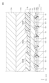
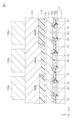
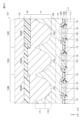
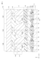
次に、例えばフォトリソグラフィ技術により、第2感光性樹脂層174をパターニングすることにより、図7に示されるように、複数の構造体170aを第1感光性樹脂層173の第1面上に形成する。構造体170aは、例えば、六角柱状体である。次に、例えばリフロー処理(加熱処理)により、図8に示されるように、複数の構造体170aを溶融し凸湾曲面状にした後、硬化させる。次に、例えば異方性ドライエッチングにより、複数の構造体170aの凸状曲面および構造体170a間に位置する第1感光性樹脂層173をエッチバックする。これにより、図9に示されるように、複数のレンズ170が形成される。
(封止工程)
次に、例えばODF(One Drop Fill)法により、以下のようにして駆動基板11と基板19とを貼り合せる。レンズアレイ17の第1面に充填樹脂を塗布し、基板19を充填樹脂上に載置する。載置後、例えば充填樹脂に熱を加えるか、または充填樹脂に紫外線を照射し、充填樹脂を硬化させることにより、充填樹脂を介して駆動基板11と基板19とを貼り合せる。これにより、表示装置101が封止される。なお、充填樹脂が熱硬化性樹脂および紫外線硬化性樹脂の両方を含む場合には、充填樹脂に紫外線を照射し仮硬化させた後、充填樹脂に熱を加えて本硬化させるようにしてもよい。以上の工程により、図4に示される表示装置101が得られる。
次に、例えばODF(One Drop Fill)法により、以下のようにして駆動基板11と基板19とを貼り合せる。レンズアレイ17の第1面に充填樹脂を塗布し、基板19を充填樹脂上に載置する。載置後、例えば充填樹脂に熱を加えるか、または充填樹脂に紫外線を照射し、充填樹脂を硬化させることにより、充填樹脂を介して駆動基板11と基板19とを貼り合せる。これにより、表示装置101が封止される。なお、充填樹脂が熱硬化性樹脂および紫外線硬化性樹脂の両方を含む場合には、充填樹脂に紫外線を照射し仮硬化させた後、充填樹脂に熱を加えて本硬化させるようにしてもよい。以上の工程により、図4に示される表示装置101が得られる。
[作用効果]
一実施形態に係る表示装置101では、下部171はテーパー状の側面を有するため、隣接するレンズ41間の距離を低減しても、隣接するレンズ41の下部171の側面同士の接近を抑制することができる。したがって、隣接するレンズ41の一方の下部171から他方の下部171に光Lが漏れ難くなり、レンズ41の下部171のレンズとしての機能低下を抑制することができる。したがって、レンズ41の光取り出し機能を向上させることができる。
一実施形態に係る表示装置101では、下部171はテーパー状の側面を有するため、隣接するレンズ41間の距離を低減しても、隣接するレンズ41の下部171の側面同士の接近を抑制することができる。したがって、隣接するレンズ41の一方の下部171から他方の下部171に光Lが漏れ難くなり、レンズ41の下部171のレンズとしての機能低下を抑制することができる。したがって、レンズ41の光取り出し機能を向上させることができる。
レンズの形成方法としては、リフロー処理のみにより、凸湾曲面状のレンズを形成するものがある。しかしながら、この方法では、隣接するレンズ間の距離を狭くした場合には、リフロー処理時にレンズの形成材料が流動し、レンズ間の谷部が埋まり、レンズ形状が崩れてしまう。
一方、一実施形態に係る表示装置では、リフロー処理により、図8に示されるように、複数の構造体170aを溶融し凸湾曲面状にした後、異方性ドライエッチング等により、図9に示されるように、複数の構造体170aの凸状曲面および構造体170a間に位置する第1感光性樹脂層173をエッチバックする。このため、レンズ170の形状崩れを抑制することができる。
一方、一実施形態に係る表示装置では、リフロー処理により、図8に示されるように、複数の構造体170aを溶融し凸湾曲面状にした後、異方性ドライエッチング等により、図9に示されるように、複数の構造体170aの凸状曲面および構造体170a間に位置する第1感光性樹脂層173をエッチバックする。このため、レンズ170の形状崩れを抑制することができる。
<4 変形例>
[変形例1]
一実施形態では、カラーフィルタ16がオンチップカラーフィルタである例について説明した。しかしながら、表示装置101の構成はこの例に限定されるものではない。例えば、図10に示されるように、基板19の第2面上にカラーフィルタ16、レンズアレイ17が順に設けられていてもよい。この場合、複数のレンズ170は、レンズ面が発光素子12側となるように配置されていてもよい。充填樹脂層20が、保護層14とレンズアレイ17の間に設けられていてもよい。レンズ170の屈折率n1は、充填樹脂層20の屈折率n2に比べて大きいことが好ましい。レンズ170の屈折率n1が充填樹脂層18の屈折率n2に比べて大きいことで、下部171のテーパー面および上部172の凸状曲面にて光を屈折させ正面方向に立ち上げることができる。したがって、光取り出し機能を向上させることができる。
[変形例1]
一実施形態では、カラーフィルタ16がオンチップカラーフィルタである例について説明した。しかしながら、表示装置101の構成はこの例に限定されるものではない。例えば、図10に示されるように、基板19の第2面上にカラーフィルタ16、レンズアレイ17が順に設けられていてもよい。この場合、複数のレンズ170は、レンズ面が発光素子12側となるように配置されていてもよい。充填樹脂層20が、保護層14とレンズアレイ17の間に設けられていてもよい。レンズ170の屈折率n1は、充填樹脂層20の屈折率n2に比べて大きいことが好ましい。レンズ170の屈折率n1が充填樹脂層18の屈折率n2に比べて大きいことで、下部171のテーパー面および上部172の凸状曲面にて光を屈折させ正面方向に立ち上げることができる。したがって、光取り出し機能を向上させることができる。
上記構成を有する表示装置101は、例えば、以下のようにして作製される。カラーフィルタ16、レンズアレイ17を基板19の第2面上に順に積層する。第2電極123の第1面上に保護層14を形成した後、保護層14の第1面に充填樹脂を塗布し、レンズアレイ17が充填樹脂側となるように、基板19を充填樹脂上に載置する。載置後、例えば充填樹脂に熱を加えるか、または充填樹脂に紫外線を照射し、充填樹脂を硬化させることにより、充填樹脂を介して駆動基板11と基板19とを貼り合せる。
一実施形態に係る表示装置101の製造工程では、レンズアレイ17が駆動基板11側に形成される。このため、レンズアレイ17の形成工程等は、加熱によるOLED層122の特性低下を考慮して、低温プロセスであることが望ましい。一方、変形例1に係る表示装置101の製造工程では、レンズアレイ17が基板19の側に形成される。このため、レンズアレイ17の形成工程等は、加熱によるOLED層122の特性低下を考慮しなくてもよく、低温プロセスでなくてもよい。したがって、表示装置101の製造が容易になる。
[変形例2]
図11に示されるように、カラーフィルタ16がレンズアレイ17の上側に設けられていてもよい。すなわち、レンズアレイ17が、複数の発光素子12とカラーフィルタ16の間に設けられていてもよい。この場合、レンズアレイ17、平坦化層21、カラーフィルタ16、充填樹脂層18、基板19が保護層14の第1面上に順に設けられていてもよい。
図11に示されるように、カラーフィルタ16がレンズアレイ17の上側に設けられていてもよい。すなわち、レンズアレイ17が、複数の発光素子12とカラーフィルタ16の間に設けられていてもよい。この場合、レンズアレイ17、平坦化層21、カラーフィルタ16、充填樹脂層18、基板19が保護層14の第1面上に順に設けられていてもよい。
変形例2に係る表示装置101では、発光素子12からレンズアレイ17までの距離を近くすることができるため、発光素子12からレンズ170に入射される光量を増加させることができる。したがって、表示装置101の正面輝度を向上させることができる。
[変形例3]
図12に示されるように、レンズ170が微細な凹凸をレンズ面に有していてもよい。レンズ170の上部172が、上記凹凸を有していてもよいし、レンズ170の上部172と下部171の両方が、上記凹凸を有していてもよい。レンズ170が微細な凹凸をレンズ面に有していてことで、レンズ170から出射される光を微細な凹凸により散乱することができる。したがって、光取り出し機能をさらに向上させることができる。
図12に示されるように、レンズ170が微細な凹凸をレンズ面に有していてもよい。レンズ170の上部172が、上記凹凸を有していてもよいし、レンズ170の上部172と下部171の両方が、上記凹凸を有していてもよい。レンズ170が微細な凹凸をレンズ面に有していてことで、レンズ170から出射される光を微細な凹凸により散乱することができる。したがって、光取り出し機能をさらに向上させることができる。
[変形例4]
図13に示されるように、レンズ170が底部175をさらに含んでもよい。底部175は、下部171の下に設けられる。底部175は、曲面状の側面を有することが好ましい。当該曲面状の側面は、下部171のテーパー状の側面よりもなだらかな傾きを持っている。隣接するレンズ170の底部175間に溝176が形成されている。溝176の断面形状は、下に凸の曲線状であることが好ましい。下部171と底部175は、滑らかに繋がっていることが好ましい。底部175は下部171と同一の材料により構成されていてもよい。
図13に示されるように、レンズ170が底部175をさらに含んでもよい。底部175は、下部171の下に設けられる。底部175は、曲面状の側面を有することが好ましい。当該曲面状の側面は、下部171のテーパー状の側面よりもなだらかな傾きを持っている。隣接するレンズ170の底部175間に溝176が形成されている。溝176の断面形状は、下に凸の曲線状であることが好ましい。下部171と底部175は、滑らかに繋がっていることが好ましい。底部175は下部171と同一の材料により構成されていてもよい。
上記のように、レンズ170が底部175をさらに含むことで、隣接するレンズ170間の谷部に対する充填樹脂の充填性を向上させることができる。
[変形例5]
図14に示されるように、レンズアレイ17に含まれる少なくとも一部のレンズ170の中心軸LN”が、発光素子12の中心軸LNを基準にして駆動基板11の第1面の面内方向(中心軸LN”に対して垂直な方向)にずれていてもよい。このようにレンズ170の中心軸LN”が駆動基板11の第1面の面内方向にずれていることで、レンズ170からの光の出射方向を制御することができる。なお、カラーフィルタ16に含まれる少なくとも一部の着色層160の中心軸が、発光素子12の中心軸LNを基準にして駆動基板11の第1面の面内方向(中心軸LN”に対して垂直な方向)にずれていてもよい。
図14に示されるように、レンズアレイ17に含まれる少なくとも一部のレンズ170の中心軸LN”が、発光素子12の中心軸LNを基準にして駆動基板11の第1面の面内方向(中心軸LN”に対して垂直な方向)にずれていてもよい。このようにレンズ170の中心軸LN”が駆動基板11の第1面の面内方向にずれていることで、レンズ170からの光の出射方向を制御することができる。なお、カラーフィルタ16に含まれる少なくとも一部の着色層160の中心軸が、発光素子12の中心軸LNを基準にして駆動基板11の第1面の面内方向(中心軸LN”に対して垂直な方向)にずれていてもよい。
[変形例6]
上記一実施形態では、複数の副画素10がデルタ配列されている例について説明した。しかしながら、複数の副画素10の配列パターンはこの例に限定されるものではない。複数の副画素10は、例えば、正方配列またはストライプ配列されていてもよい。
上記一実施形態では、複数の副画素10がデルタ配列されている例について説明した。しかしながら、複数の副画素10の配列パターンはこの例に限定されるものではない。複数の副画素10は、例えば、正方配列またはストライプ配列されていてもよい。
(正方配列の例)
複数の副画素10の配列パターンが正方配列の場合、図15Aに示されるように、1画素10Pが4つの副画素10R、10G、10B、10Bにより構成されていてもよい。1画素10Pに含まれる副画素10Rと副画素10Gが、斜め方向に隣接するように配置され、かつ、1画素10Pに含まれる副画素10Bと副画素10Bが、斜め方向に隣接するように配置されていてもよい。但し、正方配列を構成する副画素10の種類および配置は、この例に限定されるものではない。
複数の副画素10の配列パターンが正方配列の場合、図15Aに示されるように、1画素10Pが4つの副画素10R、10G、10B、10Bにより構成されていてもよい。1画素10Pに含まれる副画素10Rと副画素10Gが、斜め方向に隣接するように配置され、かつ、1画素10Pに含まれる副画素10Bと副画素10Bが、斜め方向に隣接するように配置されていてもよい。但し、正方配列を構成する副画素10の種類および配置は、この例に限定されるものではない。
副画素10は、図15Aに示されるように、平面視において正方形状を有していてもよいし、図15Bに示されるように、正方形状の角が丸くなった形状を有していてもよい。レンズ170の底面は、図15Aに示されるように、平面視において正方形状を有していてもよいし、図15Bに示されるように、正方形状の角が丸くなった形状を有していてもよい。正方形状は、四角形状の一例である。なお、図15Aおよび図15Bでは、平面視におけるレンズ170の底面形状と副画素10の形状が同一であり、かつ、レンズ170の底面と副画素10のサイズが同一である例が示されている。隣接するレンズ170間の隙間の面積を低減するためには、隣接するレンズ170の底面の辺同士が、平面視において接していることが好ましい。
(ストライプ配列の例)
複数の副画素10の配列パターンがストライプ配列の場合、図16Aに示されるように、1画素10Pが3つの副画素10R、10G、10Bにより構成されていてもよい。
複数の副画素10の配列パターンがストライプ配列の場合、図16Aに示されるように、1画素10Pが3つの副画素10R、10G、10Bにより構成されていてもよい。
副画素10は、図16Aに示されるように、平面視において長方形状を有していてもよいし、図16Bに示されるように、長方形状の角が丸くなった形状を有していてもよい。レンズ170の底面は、図16Aに示されるように、平面視において長方形状を有していてもよいし、図16Bに示されるように、長方形状の角が丸くなった形状を有していてもよい。長方形状は、四角形状の一例である。なお、図16Aおよび図16Bでは、平面視におけるレンズ170の底面形状と副画素10の形状が同一であり、かつ、レンズ170の底面と副画素10のサイズが同一である例が示されている。隣接するレンズ170間の隙間の面積を低減するためには、隣接するレンズ170の底面の辺同士が、平面視において接していることが好ましい。
図16A、図16Bでは、3つの副画素10R、10G、10Bのサイズが同一である例が示されている。しかしながら、3つの副画素10R、10G、10Bのサイズはこの例に限定されるものではなく、異なっていてもよい。例えば、図17A、図17Bに示されるように、X軸方向における副画素10R、10Gのサイズが、X軸方向における副画素10Bのサイズに比べて小さくてもよい。同様に、3つの副画素10R、10G、10Bそれぞれに設けられたレンズ170のサイズが異なっていてもよい。
図17A、図17Bでは、ストライプ配列された副画素10R、10G、10Bのサイズが異なる例が示されているが、デルタ配列された副画素10R、10G、10Bまたは正方配列された副画素10R、10G、10B、10B等のサイズが異なっていてもよい。同様に、デルタ配列された副画素10R、10G、10Bにそれぞれ設けられたレンズ170のサイズが異なっていてもよいし、正方配列された副画素10R、10G、10B、10Bにそれぞれ設けられたレンズ170のサイズが異なっていてもよい。
[変形例7]
一実施形態においては、平面視における副画素10の形状およびレンズ170の底面の形状が六角形状である例について説明した。また、変形例6においては、平面視における副画素10の形状およびレンズ170の底面の形状が、正方形状または長方形状であり例について説明した。しかしながら、平面視における副画素10の形状およびレンズ170の底面の形状はこれらの例に限定されるものではなく、例えば、図18に示されるように、円形状であってもよいし、楕円形状であってもよい。
一実施形態においては、平面視における副画素10の形状およびレンズ170の底面の形状が六角形状である例について説明した。また、変形例6においては、平面視における副画素10の形状およびレンズ170の底面の形状が、正方形状または長方形状であり例について説明した。しかしながら、平面視における副画素10の形状およびレンズ170の底面の形状はこれらの例に限定されるものではなく、例えば、図18に示されるように、円形状であってもよいし、楕円形状であってもよい。
但し、副画素10が円形状または楕円形状を有する場合において、隣接する副画素10を近づけると、図18に示されるように、隣接する副画素10同士は点で接することになる。一方、副画素10が六角形状、正方形状または長方形状を有する場合において、隣接する副画素10を近づけた場合には、図3A、図15A、図16Aに示されるように、副画素10同士は辺で接することになる。このため、隣接する副画素10間の隙間の面積を低減する観点からすると、平面視における副画素10の形状は、六角形状、正方形状または長方形状であることが好ましい。同様に、隣接するレンズ170間の隙間の面積を低減する観点からすると、平面視におけるレンズ170の形状は、六角形状、正方形状または長方形状であることが好ましい。
[変形例8]
一実施形態では、レンズアレイ17の第1面上に充填樹脂層18、基板19が順に設けられている例について説明した。しかしながら、表示装置101の構成はこの例に限定されるものではなく、レンズアレイ17の第1面上に充填樹脂層18、基板19が設けられず、レンズアレイ17の第1面が解放されていてもよい。
一実施形態では、レンズアレイ17の第1面上に充填樹脂層18、基板19が順に設けられている例について説明した。しかしながら、表示装置101の構成はこの例に限定されるものではなく、レンズアレイ17の第1面上に充填樹脂層18、基板19が設けられず、レンズアレイ17の第1面が解放されていてもよい。
[変形例9]
光取出し効率の向上および/または色純度の向上の観点から、発光素子12が共振器構造を有していてもよい。本明細書において「および/または」とは、少なくとも一方を意味し、例えば、「Xおよび/またはY」の場合、Xのみ、Yのみ、XおよびYの三通りを意味するものである。
光取出し効率の向上および/または色純度の向上の観点から、発光素子12が共振器構造を有していてもよい。本明細書において「および/または」とは、少なくとも一方を意味し、例えば、「Xおよび/またはY」の場合、Xのみ、Yのみ、XおよびYの三通りを意味するものである。
第1電極121が反射層としての機能を有する反射電極である場合、第1電極121と第2電極123とにより共振器構造が構成されてもよい。この場合、第1電極121と第2電極123との間の光学的距離は、OLED層122の厚さにより設定されていてもよいし、第1電極121の材料の選択により設定されてもよいし、これらの組み合わせにより設定されてもよい。
第1電極121が透明電極である場合、当該透明電極の下方に反射層を備え、当該反射層と第2電極123とにより共振器構造が構成されてもよい。この場合、反射層と第2電極123との間の光学的距離は、OLED層122の厚さにより設定されていてもよいし、反射層の材料の選択により設定されてもよいし、第1電極121(透明電極)と反射層との間に設けられた絶縁層の厚さにより設定されてもよいし、これらの2以上の組み合わせにより設定されてもよい。
[変形例10]
一実施形態では、表示装置101が、白色光を発光することができる複数の発光素子12とカラーフィルタ16とを備え、これらの組み合わせによりカラー画像を表示することができる例について説明したが、表示装置101のカラー化の方式はこれに限定されるものではない。例えば、表示装置101が、複数の発光素子12に代えて、赤色光を発光することができる複数の発光素子と、緑色光を発光することができる複数の発光素子と、青色光を発光することができる複数の発光素子を備えてもよい。この場合、カラーフィルタは備えられていてもよいし、備えられていなくてもよい。
一実施形態では、表示装置101が、白色光を発光することができる複数の発光素子12とカラーフィルタ16とを備え、これらの組み合わせによりカラー画像を表示することができる例について説明したが、表示装置101のカラー化の方式はこれに限定されるものではない。例えば、表示装置101が、複数の発光素子12に代えて、赤色光を発光することができる複数の発光素子と、緑色光を発光することができる複数の発光素子と、青色光を発光することができる複数の発光素子を備えてもよい。この場合、カラーフィルタは備えられていてもよいし、備えられていなくてもよい。
上記発光素子は、例えば、(1)所定色の光(赤色光、緑色光または青色光)を発光することができる発光層を含む発光素子、(2)白色光を発光することができる発光層を含み、当該発光層で発光された白色光に含まれる所定波長の光(赤色光、緑色光または青色光)を共振器構造により共振させ強調することができる発光素子、または(3)所定色の光(赤色光、緑色光または青色光)を発光することができる発光層を含み、当該発光層で発光された所定色の光に含まれる所定波長の光を共振器構造により共振させ強調することができる発光素子である。
[変形例11]
一実施形態では、カラーフィルタ16が備えられる例について説明したが、カラーフィルタ16に代えて量子ドット層が備えられてもよいし、カラーフィルタ16と共に量子ドット層が備えられてもよい。量子ドット層は、量子ドット(半導体粒子)を含み、複数の発光素子から出射された光の色を変換することができる。この場合、複数の発光素子12は、青色光を発光することができるように構成されていてもよい。
一実施形態では、カラーフィルタ16が備えられる例について説明したが、カラーフィルタ16に代えて量子ドット層が備えられてもよいし、カラーフィルタ16と共に量子ドット層が備えられてもよい。量子ドット層は、量子ドット(半導体粒子)を含み、複数の発光素子から出射された光の色を変換することができる。この場合、複数の発光素子12は、青色光を発光することができるように構成されていてもよい。
[変形例12]
一実施形態では、発光素子12がOLED素子である例について説明したが、発光素子はこの例に限定されるものではなく、例えば、LED(Light Emitting Diode(発光ダイオード))素子、無機エレクトロルミネッセンス(Inorganic Electro-Luminescence:IEL)素子、量子ドット発光ダイオード(Quantum Dot Light Emitting Diode:QLED)素子または半導体レーザー素子等の自発光型の発光素子等であってもよい。2種以上の発光素子が表示装置に備えられてもよい。
一実施形態では、発光素子12がOLED素子である例について説明したが、発光素子はこの例に限定されるものではなく、例えば、LED(Light Emitting Diode(発光ダイオード))素子、無機エレクトロルミネッセンス(Inorganic Electro-Luminescence:IEL)素子、量子ドット発光ダイオード(Quantum Dot Light Emitting Diode:QLED)素子または半導体レーザー素子等の自発光型の発光素子等であってもよい。2種以上の発光素子が表示装置に備えられてもよい。
[その他の変形例]
以上、本開示の一実施形態およびその変形例(以下「一実施形態等」という。)について具体的に説明したが、本開示は、一実施形態等に限定されるものではなく、本開示の技術的思想に基づく各種の変形が可能である。
以上、本開示の一実施形態およびその変形例(以下「一実施形態等」という。)について具体的に説明したが、本開示は、一実施形態等に限定されるものではなく、本開示の技術的思想に基づく各種の変形が可能である。
例えば、一実施形態等において挙げた構成、方法、工程、形状、材料および数値等はあくまでも例に過ぎず、必要に応じてこれと異なる構成、方法、工程、形状、材料および数値等を用いてもよい。
一実施形態等の構成、方法、工程、形状、材料および数値等は、本開示の主旨を逸脱しない限り、互いに組み合わせることが可能である。
一実施形態等に例示した材料は、特に断らない限り、1種を単独でまたは2種以上を組み合わせて用いることができる。
また、本開示は以下の構成を採用することもできる。
(1)
二次元配列された複数の発光素子と、
前記複数の発光素子それぞれに対応して設けられた複数のレンズと
を備え、
前記レンズは、テーパー状の側面を有する下部と、凸湾曲面状を有する上部とを含む、
表示装置。
(2)
前記側面の傾斜角θは、45°<θ<90°である、
(1)に記載の表示装置。
(3)
前記上部と前記下部が、同一材料により構成されている、
(1)または(2)に記載の表示装置。
(4)
隣接する前記レンズの底面の周縁同士が、平面視において接している、
(1)から(3)のいずれか1項に記載の表示装置。
(5)
前記複数のレンズは、平面視において略四角形状または略六角形状を有し、
隣接する前記レンズの底面の辺同士が、平面視において接している、
(1)から(3)のいずれか1項に記載の表示装置。
(6)
前記複数のレンズのうちの少なくとも一部のレンズは、前記発光素子を基準にして面内方向にずれている、
(1)から(5)のいずれか1項に記載の表示装置。
(7)
前記複数のレンズを覆う樹脂層をさらに備え、
前記レンズの屈折率は、前記樹脂層の屈折率に比べて大きい、
(1)から(6)のいずれか1項に記載の表示装置。
(8)
前記複数のレンズは、レンズ面が前記発光素子側とは反対側となるように配置されている、
(1)から(7)のいずれか1項に記載の表示装置。
(9)
前記複数のレンズは、レンズ面が前記発光素子側となるように配置されている、
(1)から(7)のいずれか1項に記載の表示装置。
(10)
前記レンズは、曲面状の側面を有する底部をさらに含み、
前記曲面状の側面は、前記下部の側面よりもなだらかな傾きを持つ、
(1)から(10)のいずれか1項に記載の表示装置。
(11)
前記複数のレンズのうちの少なくとも一部のレンズは、凹凸を表面に有する、
(1)から(10)のいずれか1項に記載の表示装置。
(12)
カラーフィルタをさらに備え、
前記複数のレンズは、前記複数の発光素子と前記カラーフィルタの間に設けられている、
(1)から(11)のいずれか1項に記載の表示装置。
(13)
前記複数の発光素子は、有機発光ダイオード素子を含む、
(1)から(12)のいずれか1項に記載の表示装置。
(14)
(1)から(13)のいずれか1項に記載の表示装置を備える電子機器。
(1)
二次元配列された複数の発光素子と、
前記複数の発光素子それぞれに対応して設けられた複数のレンズと
を備え、
前記レンズは、テーパー状の側面を有する下部と、凸湾曲面状を有する上部とを含む、
表示装置。
(2)
前記側面の傾斜角θは、45°<θ<90°である、
(1)に記載の表示装置。
(3)
前記上部と前記下部が、同一材料により構成されている、
(1)または(2)に記載の表示装置。
(4)
隣接する前記レンズの底面の周縁同士が、平面視において接している、
(1)から(3)のいずれか1項に記載の表示装置。
(5)
前記複数のレンズは、平面視において略四角形状または略六角形状を有し、
隣接する前記レンズの底面の辺同士が、平面視において接している、
(1)から(3)のいずれか1項に記載の表示装置。
(6)
前記複数のレンズのうちの少なくとも一部のレンズは、前記発光素子を基準にして面内方向にずれている、
(1)から(5)のいずれか1項に記載の表示装置。
(7)
前記複数のレンズを覆う樹脂層をさらに備え、
前記レンズの屈折率は、前記樹脂層の屈折率に比べて大きい、
(1)から(6)のいずれか1項に記載の表示装置。
(8)
前記複数のレンズは、レンズ面が前記発光素子側とは反対側となるように配置されている、
(1)から(7)のいずれか1項に記載の表示装置。
(9)
前記複数のレンズは、レンズ面が前記発光素子側となるように配置されている、
(1)から(7)のいずれか1項に記載の表示装置。
(10)
前記レンズは、曲面状の側面を有する底部をさらに含み、
前記曲面状の側面は、前記下部の側面よりもなだらかな傾きを持つ、
(1)から(10)のいずれか1項に記載の表示装置。
(11)
前記複数のレンズのうちの少なくとも一部のレンズは、凹凸を表面に有する、
(1)から(10)のいずれか1項に記載の表示装置。
(12)
カラーフィルタをさらに備え、
前記複数のレンズは、前記複数の発光素子と前記カラーフィルタの間に設けられている、
(1)から(11)のいずれか1項に記載の表示装置。
(13)
前記複数の発光素子は、有機発光ダイオード素子を含む、
(1)から(12)のいずれか1項に記載の表示装置。
(14)
(1)から(13)のいずれか1項に記載の表示装置を備える電子機器。
<5 発光部、レンズ部材、波長選択部のそれぞれの中心を通る法線の関係>
以下、発光部の中心を通る法線LNと、レンズ部材の中心を通る法線LN’と、波長選択部の中心を通る法線LN”との関係を説明する。ここで、発光部は、例えば、一実施形態等における発光素子12である。レンズ部材は、例えば、一実施形態等におけるレンズ170である。波長選択部は、例えば、一実施形態等における着色層160である。
以下、発光部の中心を通る法線LNと、レンズ部材の中心を通る法線LN’と、波長選択部の中心を通る法線LN”との関係を説明する。ここで、発光部は、例えば、一実施形態等における発光素子12である。レンズ部材は、例えば、一実施形態等におけるレンズ170である。波長選択部は、例えば、一実施形態等における着色層160である。
なお、発光部が出射する光に対応して、波長選択部の大きさを、適宜、変えてもよいし、隣接する発光部の波長選択部の間に光吸収部(例えば、ブラックマトリクス部)が設けられている場合、発光部が出射する光に対応して、光吸収部の大きさを、適宜、変えてもよい。また、波長選択部の大きさを、発光部の中心を通る法線と波長選択部の中心を通る法線との間の距離(オフセット量)d0に応じて、適宜、変えてもよい。波長選択部の平面形状は、レンズ部材の平面形状と同じであってもよいし、相似であってもよいし、異なっていてもよい。
以下、図19A、図19B、図19C、図20を参照して、発光部51と、波長選択部52、レンズ部材53が、この順序で配置されている場合の各部の中心を通る法線の関係について説明する。
図19Aに示されるように、発光部51の中心を通る法線LNと、波長選択部52の中心を通る法線LN”と、レンズ部材53の中心を通る法線LN’とは、一致していてもよい。すなわち、D0=0、d0=0であってもよい。但し、D0は、発光部51の中心を通る法線LNとレンズ部材53の中心を通る法線LN’との間の距離(オフセット量)を表し、d0は、発光部51の中心を通る法線LNと波長選択部52の中心を通る法線LN”との間の距離(オフセット量)を表す。
図19Bに示されるように、発光部51の中心を通る法線LNと、波長選択部52の中心を通る法線LN”とは、一致しているが、発光部51の中心を通る法線LNおよび波長選択部52の中心を通る法線LN”と、レンズ部材53の中心を通る法線LN’とは、一致していない構成としてもよい。すなわち、D0>0、d0=0であってもよい。
図19Cに示されるように、発光部51の中心を通る法線LNと、波長選択部52の中心を通る法線LN”およびレンズ部材53の中心を通る法線LN’とは、一致しておらず、波長選択部52の中心を通る法線LN”と、レンズ部材53の中心を通る法線LN’とは、一致している構成としてもよい。すなわち、D0>0、d0>0、D0=d0であってもよい。
図20に示されるように、発光部51の中心を通る法線LNと、波長選択部52の中心を通る法線LN”と、レンズ部材53の中心を通る法線LN’とがいずれも、一致していない構成としてもよい。すなわち、D0>0、d0>0、D0≠d0であってもよい。ここで、発光部51の中心とレンズ部材53の中心(図20において黒丸で示される位置)とを結ぶ直線LL上に、波長選択部52の中心(図20において黒四角で示される位置)が位置することが好ましい。具体的には、発光部51の中心と波長選択部52の中心との間の、厚さ方向(図20中、垂直方向)における距離をLL1、波長選択部52の中心とレンズ部材53の中心との間の、厚さ方向における距離をLL2としたとき、
D0>d0>0
であり、製造上のバラツキを考慮した上で、
d0:D0=LL1:(LL1+LL2)
を満足することが好ましい。
ここで、厚さ方向とは、発光部51、波長選択部52、レンズ部材53の厚さ方向を表す。
D0>d0>0
であり、製造上のバラツキを考慮した上で、
d0:D0=LL1:(LL1+LL2)
を満足することが好ましい。
ここで、厚さ方向とは、発光部51、波長選択部52、レンズ部材53の厚さ方向を表す。
以下、図21A、図21B、図22を参照して、発光部51と、レンズ部材53、波長選択部52が、この順序で配置されている場合の各部の中心を通る法線の関係について説明する。
図21Aに示されるように、発光部51の中心を通る法線LNと、波長選択部52の中心を通る法線LN”と、レンズ部材53の中心を通る法線LN’とは、一致している構成としてもよい。すなわち、D0>0、d0=0であってもよい。
図21Bに示されるように、発光部51の中心を通る法線LNと、波長選択部52の中心を通る法線LN”およびレンズ部材53の中心を通る法線LN’とは、一致しておらず、波長選択部52の中心を通る法線LN”と、レンズ部材53の中心を通る法線LN’とは、一致している構成としてもよい。すなわち、D0>0、d0>0、D0=d0であってもよい。
図22に示されるように、発光部51の中心を通る法線LNと、波長選択部52の中心を通る法線LN”と、レンズ部材53の中心を通る法線LN’とがいずれも、一致していない構成としてもよい。ここで、発光部51の中心と波長選択部52の中心(図22において黒四角で示される位置)とを結ぶ直線LL上に、レンズ部材53の中心(図22において黒丸で示される位置)が位置することが好ましい。具体的には、発光部51の中心とレンズ部材53の中心との間の、厚さ方向(図22中、垂直方向)における距離をLL2、レンズ部材53の中心と波長選択部52の中心との間の、厚さ方向における距離をLL1としたとき、
d0>D0>0
であり、製造上のバラツキを考慮した上で、
D0:d0=LL2:(LL1+LL2)
を満足することが好ましい。
ここで、厚さ方向とは、発光部51、波長選択部52、レンズ部材53の厚さ方向を表す。
d0>D0>0
であり、製造上のバラツキを考慮した上で、
D0:d0=LL2:(LL1+LL2)
を満足することが好ましい。
ここで、厚さ方向とは、発光部51、波長選択部52、レンズ部材53の厚さ方向を表す。
<6 共振器構造の例>
一実施形態等に係る表示装置101に含まれる副画素10は、発光素子12で発生した光を共振させる共振器構造を備えている構成とすることができる。以下、図面を参照しながら、共振器構造について説明する。また、以下の説明において、各層の第1面を上面ということがある。
一実施形態等に係る表示装置101に含まれる副画素10は、発光素子12で発生した光を共振させる共振器構造を備えている構成とすることができる。以下、図面を参照しながら、共振器構造について説明する。また、以下の説明において、各層の第1面を上面ということがある。
(共振器構造:第1例)
図23Aは、共振器構造の第1例を説明するための模式的な断面図である。以下の説明において、副画素10R、10G、10Bにそれぞれに対応して設けられた発光素子を特に区別せず総称する場合には、それらの発光素子を発光素子12ということがある。副画素10R、10G、10Bにそれぞれに対応して設けられた発光素子を区別する場合には、それらの発光素子を発光素子12R、12G、12Bということがある。OLED層122のうち副画素10R、10G、10Bにそれぞれに対応する部分を、OLED層122R、OLED層122G、OLED層122Bということがある。
図23Aは、共振器構造の第1例を説明するための模式的な断面図である。以下の説明において、副画素10R、10G、10Bにそれぞれに対応して設けられた発光素子を特に区別せず総称する場合には、それらの発光素子を発光素子12ということがある。副画素10R、10G、10Bにそれぞれに対応して設けられた発光素子を区別する場合には、それらの発光素子を発光素子12R、12G、12Bということがある。OLED層122のうち副画素10R、10G、10Bにそれぞれに対応する部分を、OLED層122R、OLED層122G、OLED層122Bということがある。
第1例において、第1電極121は各発光素子12において共通の膜厚で形成されている。第2電極123においても同様である。
発光素子12の第1電極121の下に、光学調整層72を挟んだ状態で、反射板71が配されている。反射板71と第2電極123との間にOLED層122が発生する光を共振させる共振器構造が形成される。以下の説明において、副画素10R、10G、10Bにそれぞれに対応して設けられた光学調整層72を、光学調整層72R、72G、72Bということがある。
反射板71は各発光素子12において共通の膜厚で形成されている。光学調整層72の膜厚は、副画素が表示すべき色に応じて異なっている。光学調整層72R、72G、72Bが異なる膜厚を有することにより、表示すべき色に応じた光の波長に最適な共振を生ずる光学的距離を設定することができる。
図23Aに示す例では、発光素子12R、12G、12Bにおける反射板71の上面は揃うように配置されている。上述したように、光学調整層72の膜厚は、副画素が表示すべき色に応じて異なっているので、第2電極123の上面の位置は、発光素子12R、12G、12Bの種類に応じて相違する。
反射板71は、例えば、アルミニウム(Al)、銀(Ag)、銅(Cu)等の金属、あるいは、これらを主成分とする合金を用いて形成することができる。
光学調整層72は、シリコン窒化物(SiNx)、シリコン酸化物(SiOx)、シリコン酸窒化物(SiOxNy)等の無機絶縁材料や、アクリル系樹脂やポリイミド系樹脂等といった有機樹脂材料を用いて構成することができる。光学調整層72は単層でも良いし、これら複数の材料の積層膜であってもよい。また、発光素子12の種類に応じて積層数が異なっても良い。
第1電極121は、インジウムスズ酸化物(ITO)やインジウム亜鉛酸化物(IZO)、亜鉛酸化物(ZnO)等の透明導電材料を用いて形成することができる。
第2電極123は、半透過反射膜として機能する必要がある。第2電極123は、マグネシウム(Mg)や銀(Ag)、またはこれらを主成分とするマグネシウム銀合金(MgAg)、さらには、アルカリ金属やアルカリ土類金属を含んだ合金等を用いて形成することができる。
(共振器構造:第2例)
図23Bは、共振器構造の第2例を説明するための模式的な断面図である。
図23Bは、共振器構造の第2例を説明するための模式的な断面図である。
第2例においても、第1電極121や第2電極123は各発光素子12において共通の膜厚で形成されている。
そして、第2例においても、発光素子12の第1電極121の下に、光学調整層72を挟んだ状態で、反射板71が配される。反射板71と第2電極123との間にOLED層122が発生する光を共振させる共振器構造が形成される。第1例と同様に、反射板71は各発光素子12において共通の膜厚で形成されており、光学調整層72の膜厚は、副画素が表示すべき色に応じて異なっている。
図23Aに示す第1例においては、発光素子12R、12G、12Bにおける反射板71の上面は揃うように配置され、第2電極123の上面の位置は、発光素子12R、12G、12Bの種類に応じて相違していた。
これに対し、図23Bに示す第2例において、第2電極123の上面は、発光素子12R、12G、12Bで揃うように配置されている。第2電極123の上面を揃えるために、発光素子12R、12G、12Bにおいて反射板71の上面は、発光素子12R、12G、12Bの種類に応じて異なるように配置されている。このため、反射板71の下面(換言すれば、下地層(絶縁層)73の上面)は、発光素子12の種類に応じた階段形状となる。
反射板71、光学調整層72、第1電極121および第2電極123を構成する材料等については、第1例において説明した内容と同様であるので、説明を省略する。
(共振器構造:第3例)
図24Aは、共振器構造の第3例を説明するための模式的な断面図である。以下の説明において、副画素10R、10G、10Bにそれぞれに対応して設けられた反射板71を、反射板71R、71G、71Bということがある。
図24Aは、共振器構造の第3例を説明するための模式的な断面図である。以下の説明において、副画素10R、10G、10Bにそれぞれに対応して設けられた反射板71を、反射板71R、71G、71Bということがある。
第3例においても、第1電極121や第2電極123は各発光素子12において共通の膜厚で形成されている。
そして、第3例においても、発光素子12の第1電極121の下に、光学調整層72を挟んだ状態で、反射板71が配される。反射板71と第2電極123との間に、OLED層122が発生する光を共振させる共振器構造が形成される。第1例や第2例と同様に、光学調整層72の膜厚は、副画素が表示すべき色に応じて異なっている。そして、第2例と同様に、第2電極123の上面の位置は、発光素子12R、12G、12Bで揃うように配置されている。
図24Bに示す第2例にあっては、第2電極123の上面を揃えるために、反射板71の下面は、発光素子12の種類に応じた階段形状であった。
これに対し、図24Aに示す第3例において、反射板71の膜厚は、発光素子12R、12G、12Bの種類に応じて異なるように設定されている。より具体的には、反射板71R、71G、71Bの下面が揃うように膜厚が設定されている。
反射板71、光学調整層72、第1電極121および第2電極123を構成する材料等については、第1例において説明した内容と同様であるので、説明を省略する。
(共振器構造:第4例)
図24Bは、共振器構造の第4例を説明するための模式的な断面図である。以下の説明において、副画素10R、10G、10Bにそれぞれに対応して設けられた第1電極121を、第1電極121R、121G、121Bということがある。
図24Bは、共振器構造の第4例を説明するための模式的な断面図である。以下の説明において、副画素10R、10G、10Bにそれぞれに対応して設けられた第1電極121を、第1電極121R、121G、121Bということがある。
図24Aに示す第1例において、各発光素子12の第1電極121や第2電極123は、共通の膜厚で形成されている。そして、発光素子12の第1電極121の下に、光学調整層72を挟んだ状態で、反射板71が配されている。
これに対し、図24Bに示す第4例では、光学調整層72を省略し、第1電極121の膜厚を、発光素子12R、12G、12Bの種類に応じて異なるように設定した。
反射板71は各発光素子12において共通の膜厚で形成されている。第1電極121の膜厚は、副画素が表示すべき色に応じて異なっている。第1電極121R、121G、121Bが異なる膜厚を有することにより、表示すべき色に応じた光の波長に最適な共振を生ずる光学的距離を設定することができる。
反射板71、光学調整層72、第1電極121および第2電極123を構成する材料等については、第1例において説明した内容と同様であるので、説明を省略する。
(共振器構造:第5例)
図25Aは、共振器構造の第5例を説明するための模式的な断面図である。
図25Aは、共振器構造の第5例を説明するための模式的な断面図である。
図23Aに示す第1例において、第1電極121や第2電極123は各発光素子12において共通の膜厚で形成されている。そして、発光素子12の第1電極121の下に、光学調整層72を挟んだ状態で、反射板71が配されている。
これに対し、図25Aに示す第5例にあっては、光学調整層72を省略し、代わりに、反射板71の表面に酸化膜74を形成した。酸化膜74の膜厚は、発光素子12R、12G、12Bの種類に応じて異なるように設定した。以下の説明において、副画素10R、10G、10Bにそれぞれに対応して設けられた酸化膜74を、酸化膜74R、74G、74Bということがある。
酸化膜74の膜厚は、副画素が表示すべき色に応じて異なっている。酸化膜74R、74G、74Bが異なる膜厚を有することにより、表示すべき色に応じた光の波長に最適な共振を生ずる光学的距離を設定することができる。
酸化膜74は、反射板71の表面を酸化した膜であって、例えば、アルミニウム酸化物、タンタル酸化物、チタン酸化物、マグネシウム酸化物、ジルコニウム酸化物等から構成される。酸化膜74は、反射板71と第2電極123との間の光路長(光学的距離)を調整するための絶縁膜として機能する。
発光素子12R、12G、12Bの種類に応じて膜厚が異なる酸化膜74は、例えば、以下のようにして形成することができる。
先ず、容器の中に電解液を充填し、反射板71が形成された基板を電解液の中に浸漬する。また、反射板71と対向するように電極を配置する。
そして、電極を基準として正電圧を反射板71に印加して、反射板71を陽極酸化する。陽極酸化による酸化膜の膜厚は、電極に対する電圧値に比例する。そこで、反射板71R、71G、71Bのそれぞれに発光素子12の種類に応じた電圧を印加した状態で陽極酸化を行う。これによって、膜厚の異なる酸化膜74を一括して形成することができる。
反射板71、第1電極121および第2電極123を構成する材料等については、第1例において説明した内容と同様であるので、説明を省略する。
(共振器構造:第6例)
図25Bは、共振器構造の第6例を説明するための模式的な断面図である。
図25Bは、共振器構造の第6例を説明するための模式的な断面図である。
第6例において、発光素子12は、第1電極121とOLED層122と第2電極123とが積層されて構成されている。但し、第6例において、第1電極121は、電極と反射板の機能を兼ねるように形成されている。第1電極(兼反射板)121は、発光素子12R、12G、12Bの種類に応じて選択された光学定数を有する材料によって形成されている。第1電極(兼反射板)121による位相シフトが異なることによって、表示すべき色に応じた光の波長に最適な共振を生ずる光学的距離を設定することができる。
第1電極(兼反射板)121は、アルミニウム(Al)、銀(Ag)、金(Au)、銅(Cu)等の単体金属や、これらを主成分とする合金から構成することができる。例えば、発光素子12Rの第1電極(兼反射板)121Rを銅(Cu)で形成し、発光素子12Gの第1電極(兼反射板)121Gと発光素子12Bの第1電極(兼反射板)121Bとをアルミニウムで形成するといった構成とすることができる。
第2電極123を構成する材料等については、第1例において説明した内容と同様であるので、説明を省略する。
(共振器構造:第7例)
図26は、共振器構造の第7例を説明するための模式的な断面図である。
図26は、共振器構造の第7例を説明するための模式的な断面図である。
第7例は、基本的には、発光素子12R、12Gについては第6例を適用し、発光素子12Bについては第1例を適用したといった構成である。この構成においても、表示すべき色に応じた光の波長に最適な共振を生ずる光学的距離を設定することができる。
発光素子12R、12Gに用いられる第1電極(兼反射板)121R、121Gは、アルミニウム(Al)、銀(Ag)、金(Au)、銅(Cu)等の単体金属や、これらを主成分とする合金から構成することができる。
発光素子12Bに用いられる、反射板71B、光学調整層72Bおよび第1電極121Bを構成する材料等については、第1例において説明した内容と同様であるので、説明を省略する。
<7 応用例>
(電子機器)
一実施形態等に係る表示装置101は、各種の電子機器に備えられてもよい。一実施形態等に係る表示装置101は、特にヘッドマウント型ディスプレイ等のアイウェアデバイス、またはビデオカメラもしくは一眼レフカメラの電子ビューファインダ等の高解像度が要求され、目の近くで拡大して使用されるものに適する。
(電子機器)
一実施形態等に係る表示装置101は、各種の電子機器に備えられてもよい。一実施形態等に係る表示装置101は、特にヘッドマウント型ディスプレイ等のアイウェアデバイス、またはビデオカメラもしくは一眼レフカメラの電子ビューファインダ等の高解像度が要求され、目の近くで拡大して使用されるものに適する。
(具体例1)
図27A、図27Bは、デジタルスチルカメラ310の外観の一例を示す。このデジタルスチルカメラ310は、レンズ交換式一眼レフレックスタイプのものであり、カメラ本体部(カメラボディ)311の正面略中央に交換式の撮影レンズユニット(交換レンズ)312を有し、正面左側に撮影者が把持するためのグリップ部313を有している。
図27A、図27Bは、デジタルスチルカメラ310の外観の一例を示す。このデジタルスチルカメラ310は、レンズ交換式一眼レフレックスタイプのものであり、カメラ本体部(カメラボディ)311の正面略中央に交換式の撮影レンズユニット(交換レンズ)312を有し、正面左側に撮影者が把持するためのグリップ部313を有している。
カメラ本体部311の背面中央から左側にずれた位置には、モニタ314が設けられている。モニタ314の上部には、電子ビューファインダ(接眼窓)315が設けられている。撮影者は、電子ビューファインダ315を覗くことによって、撮影レンズユニット312から導かれた被写体の光像を視認して構図決定を行うことが可能である。電子ビューファインダ315は、一実施形態等に係る表示装置101のうちいずれかを備える。
(具体例2)
図28は、ヘッドマウントディスプレイ320の外観の一例を示す。ヘッドマウントディスプレイ320は、アイウェアデバイスの一例である。ヘッドマウントディスプレイ320は、例えば、眼鏡形の表示部321の両側に、使用者の頭部に装着するための耳掛け部322を有している。表示部321は、一実施形態等に係る表示装置101のうちいずれかを備える。
図28は、ヘッドマウントディスプレイ320の外観の一例を示す。ヘッドマウントディスプレイ320は、アイウェアデバイスの一例である。ヘッドマウントディスプレイ320は、例えば、眼鏡形の表示部321の両側に、使用者の頭部に装着するための耳掛け部322を有している。表示部321は、一実施形態等に係る表示装置101のうちいずれかを備える。
(具体例3)
図29は、テレビジョン装置330の外観の一例を示す。このテレビジョン装置330は、例えば、フロントパネル332およびフィルターガラス333を含む映像表示画面部331を有しており、この映像表示画面部331は、一実施形態等に係る表示装置101のうちいずれかを備える。
図29は、テレビジョン装置330の外観の一例を示す。このテレビジョン装置330は、例えば、フロントパネル332およびフィルターガラス333を含む映像表示画面部331を有しており、この映像表示画面部331は、一実施形態等に係る表示装置101のうちいずれかを備える。
(具体例4)
図30は、シースルーヘッドマウントディスプレイ340の外観の一例を示す。シースルーヘッドマウントディスプレイ340は、アイウェアデバイスの一例である。シースルーヘッドマウントディスプレイ340は、本体部341と、アーム342と、鏡筒343とを備える。
図30は、シースルーヘッドマウントディスプレイ340の外観の一例を示す。シースルーヘッドマウントディスプレイ340は、アイウェアデバイスの一例である。シースルーヘッドマウントディスプレイ340は、本体部341と、アーム342と、鏡筒343とを備える。
本体部341は、アーム342および眼鏡350と接続される。具体的には、本体部341の長辺方向の端部はアーム342と結合され、本体部341の側面の一側は接続部材を介して眼鏡350と連結される。なお、本体部341は、直接的に人体の頭部に装着されてもよい。
本体部341は、シースルーヘッドマウントディスプレイ340の動作を制御するための制御基板や、表示部を内蔵する。アーム342は、本体部341と鏡筒343とを接続させ、鏡筒343を支える。具体的には、アーム342は、本体部341の端部および鏡筒343の端部とそれぞれ結合され、鏡筒343を固定する。また、アーム342は、本体部341から鏡筒343に提供される画像に係るデータを通信するための信号線を内蔵する。
鏡筒343は、本体部341からアーム342を経由して提供される画像光を、接眼レンズ351を通じて、シースルーヘッドマウントディスプレイ340を装着するユーザの目に向かって投射する。このシースルーヘッドマウントディスプレイ340において、本体部341の表示部は、一実施形態等に係る表示装置101のうちいずれかを備える。
(具体例5)
図31は、スマートフォン360の外観の一例を示す。スマートフォン360は、各種情報を表示する表示部361、およびユーザによる操作入力を受け付けるボタン等から構成される操作部362等を備える。表示部361は、一実施形態等に係る表示装置101のうちいずれかを備える。
図31は、スマートフォン360の外観の一例を示す。スマートフォン360は、各種情報を表示する表示部361、およびユーザによる操作入力を受け付けるボタン等から構成される操作部362等を備える。表示部361は、一実施形態等に係る表示装置101のうちいずれかを備える。
(具体例6)
一実施形態等に係る表示装置101は、乗物に備えられる各種のディスプレイに備えられてもよい。
一実施形態等に係る表示装置101は、乗物に備えられる各種のディスプレイに備えられてもよい。
図32Aおよび図32Bは、各種のディスプレイが備えられた乗物500の内部の構成の一例を示す図である。具体的には、図32Aは、乗物500の後方から前方にかけての乗物500の内部の様子の一例を示す図、図32Bは、乗物500の斜め後方から斜め前方にかけての乗物500の内部の様子の一例を示す図である。
乗物500は、センターディスプレイ501と、コンソールディスプレイ502と、ヘッドアップディスプレイ503と、デジタルリアミラー504と、ステアリングホイールディスプレイ505と、リアエンタテイメントディスプレイ506とを備える。これらのディスプレイの少なくとも1つが、一実施形態等に係る表示装置101のうちいずれかを備える。例えば、これらのディスプレイのすべてが、一実施形態等に係る表示装置101のうちいずれかを備えてもよい。
センターディスプレイ501は、運転席508および助手席509に対向するダッシュボードの部分に配置されている。図32Aおよび図32Bでは、運転席508側から助手席509側まで延びる横長形状のセンターディスプレイ501の例を示すが、センターディスプレイ501の画面サイズや配置場所は任意である。センターディスプレイ501には、種々のセンサで検知された情報を表示可能である。具体的な一例として、センターディスプレイ501には、イメージセンサで撮影した撮影画像、ToFセンサで計測された乗物500の前方や側方の障害物までの距離画像、赤外線センサで検出された乗客の体温等を表示可能である。センターディスプレイ501は、例えば、安全関連情報、操作関連情報、ライフログ、健康関連情報、認証/識別関連情報、およびエンタテイメント関連情報の少なくとも一つを表示するために用いることができる。
安全関連情報は、居眠り検知、よそ見検知、同乗している子供のいたずら検知、シートベルト装着有無、乗員の置き去り検知等の情報であり、例えばセンターディスプレイ501の裏面側に重ねて配置されたセンサにて検知される情報である。操作関連情報は、センサを用いて乗員の操作に関するジェスチャを検知する。検知されるジェスチャは、乗物500内の種々の設備の操作を含んでもよい。例えば、空調設備、ナビゲーション装置、AV装置、照明装置等の操作を検知する。ライフログは、乗員全員のライフログを含む。例えば、ライフログは、乗車中の各乗員の行動記録を含む。ライフログを取得および保存することで、事故時に乗員がどのような状態であったかを確認できる。健康関連情報は、温度センサ等のセンサを用いて乗員の体温を検知し、検知した体温に基づいて乗員の健康状態を推測する。あるいは、イメージセンサを用いて乗員の顔を撮像し、撮像した顔の表情から乗員の健康状態を推測してもよい。さらに、乗員に対して自動音声で会話を行って、乗員の回答内容に基づいて乗員の健康状態を推測してもよい。認証/識別関連情報は、センサを用いて顔認証を行うキーレスエントリ機能や、顔識別でシート高さや位置の自動調整機能等を含む。エンタテイメント関連情報は、センサを用いて乗員によるAV装置の操作情報を検出する機能や、センサで乗員の顔を認識して、乗員に適したコンテンツをAV装置にて提供する機能等を含む。
コンソールディスプレイ502は、例えば、ライフログ情報の表示に用いることができる。コンソールディスプレイ502は、運転席508と助手席509の間のセンターコンソール510のシフトレバー511の近くに配置されている。コンソールディスプレイ502にも、種々のセンサで検知された情報を表示可能である。また、コンソールディスプレイ502には、イメージセンサで撮像された車両周辺の画像を表示してもよいし、車両周辺の障害物までの距離画像を表示してもよい。
ヘッドアップディスプレイ503は、運転席508の前方のフロントガラス512の奥に仮想的に表示される。ヘッドアップディスプレイ503は、例えば、安全関連情報、操作関連情報、ライフログ、健康関連情報、認証/識別関連情報、およびエンタテイメント関連情報の少なくとも一つを表示するために用いることができる。ヘッドアップディスプレイ503は、運転席508の正面に仮想的に配置されることが多いため、乗物500の速度や燃料(バッテリ)残量等の乗物500の操作に直接関連する情報を表示するのに適している。
デジタルリアミラー504は、乗物500の後方を表示できるだけでなく、後部座席の乗員の様子も表示できるため、デジタルリアミラー504の裏面側に重ねてセンサを配置することで、例えばライフログ情報の表示に用いることができる。
ステアリングホイールディスプレイ505は、乗物500のハンドル513の中心付近に配置されている。ステアリングホイールディスプレイ505は、例えば、安全関連情報、操作関連情報、ライフログ、健康関連情報、認証/識別関連情報、およびエンタテイメント関連情報の少なくとも一つを表示するために用いることができる。特に、ステアリングホイールディスプレイ505は、運転者の手の近くにあるため、運転者の体温等のライフログ情報を表示したり、AV装置や空調設備等の操作に関する情報等を表示するのに適している。
リアエンタテイメントディスプレイ506は、運転席508や助手席509の背面側に取り付けられており、後部座席の乗員が視聴するためのものである。リアエンタテイメントディスプレイ506は、例えば、安全関連情報、操作関連情報、ライフログ、健康関連情報、認証/識別関連情報、およびエンタテイメント関連情報の少なくとも一つを表示するために用いることができる。特に、リアエンタテイメントディスプレイ506は、後部座席の乗員の目の前にあるため、後部座席の乗員に関連する情報が表示される。例えば、AV装置や空調設備の操作に関する情報を表示したり、後部座席の乗員の体温等を温度センサで計測した結果を表示してもよい。
表示装置101等の裏面側に重ねてセンサを配置し、周囲に存在する物体までの距離を計測することができる構成としてもよい。光学的な距離計測の手法には、大きく分けて、受動型と能動型がある。受動型は、センサから物体に光を投光せずに、物体からの光を受光して距離計測を行うものである。受動型には、レンズ焦点法、ステレオ法、および単眼視法等がある。能動型は、物体に光を投光して、物体からの反射光をセンサで受光して距離計測を行うものである。能動型には、光レーダ方式、アクティブステレオ方式、照度差ステレオ法、モアレトポグラフィ法、干渉法等がある。一実施形態等に係る表示装置101は、これらのどの方式の距離計測にも適用可能である。表示装置101の裏面側に重ねて配置されるセンサを用いることで、上述した受動型または能動型の距離計測を行うことができる。
10R、10G、10B 副画素
11 駆動基板
111 基板
112 絶縁層
113 パッド部
12 発光素子
121 第1電極
122 OLED層
123 第2電極
13 絶縁層
131 開口
14 保護層
15 平坦化層
16 カラーフィルタ
160R、160G、160B 着色層
17 レンズアレイ
170 レンズ
170a 構造体
171 下部
172 上部
173 第1感光性樹脂層
174 第2感光性樹脂層
175 底部
176 溝
18 充填樹脂層
19 基板
101 表示装置
310 デジタルスチルカメラ
320 ヘッドマウントディスプレイ
330 テレビジョン装置
340 シースルーヘッドマウントディスプレイ
360 スマートフォン
500 乗物
RE1 有効画素領域
RE2 周辺領域
11 駆動基板
111 基板
112 絶縁層
113 パッド部
12 発光素子
121 第1電極
122 OLED層
123 第2電極
13 絶縁層
131 開口
14 保護層
15 平坦化層
16 カラーフィルタ
160R、160G、160B 着色層
17 レンズアレイ
170 レンズ
170a 構造体
171 下部
172 上部
173 第1感光性樹脂層
174 第2感光性樹脂層
175 底部
176 溝
18 充填樹脂層
19 基板
101 表示装置
310 デジタルスチルカメラ
320 ヘッドマウントディスプレイ
330 テレビジョン装置
340 シースルーヘッドマウントディスプレイ
360 スマートフォン
500 乗物
RE1 有効画素領域
RE2 周辺領域
Claims (14)
- 二次元配列された複数の発光素子と、
前記複数の発光素子それぞれに対応して設けられた複数のレンズと
を備え、
前記レンズは、テーパー状の側面を有する下部と、凸湾曲面状を有する上部とを含む、
表示装置。 - 前記側面の傾斜角θは、45°<θ<90°である、
請求項1に記載の表示装置。 - 前記上部と前記下部が、同一材料により構成されている、
請求項1に記載の表示装置。 - 隣接する前記レンズの底面の周縁同士が、平面視において接している、
請求項1に記載の表示装置。 - 前記複数のレンズは、平面視において略四角形状または略六角形状を有し、
隣接する前記レンズの底面の辺同士が、平面視において接している、
請求項1に記載の表示装置。 - 前記複数のレンズのうちの少なくとも一部のレンズは、前記発光素子を基準にして面内方向にずれている、
請求項1に記載の表示装置。 - 前記複数のレンズを覆う樹脂層をさらに備え、
前記レンズの屈折率は、前記樹脂層の屈折率に比べて大きい、
請求項1に記載の表示装置。 - 前記複数のレンズは、レンズ面が前記発光素子側とは反対側となるように配置されている、
請求項1に記載の表示装置。 - 前記複数のレンズは、レンズ面が前記発光素子側となるように配置されている、
請求項1に記載の表示装置。 - 前記レンズは、曲面状の側面を有する底部をさらに含み、
前記曲面状の側面は、前記下部の側面よりもなだらかな傾きを持つ、
請求項1に記載の表示装置。 - 前記複数のレンズのうちの少なくとも一部のレンズは、凹凸を表面に有する、
請求項1に記載の表示装置。 - カラーフィルタをさらに備え、
前記複数のレンズは、前記複数の発光素子と前記カラーフィルタの間に設けられている、
請求項1に記載の表示装置。 - 前記複数の発光素子は、有機発光ダイオード素子を含む、
請求項1に記載の表示装置。 - 請求項1に記載の表示装置を備える電子機器。
Priority Applications (2)
| Application Number | Priority Date | Filing Date | Title |
|---|---|---|---|
| CN202480031962.5A CN121100601A (zh) | 2023-05-29 | 2024-05-13 | 显示装置和电子设备 |
| JP2025523431A JPWO2024247697A1 (ja) | 2023-05-29 | 2024-05-13 |
Applications Claiming Priority (2)
| Application Number | Priority Date | Filing Date | Title |
|---|---|---|---|
| JP2023-088110 | 2023-05-29 | ||
| JP2023088110 | 2023-05-29 |
Publications (1)
| Publication Number | Publication Date |
|---|---|
| WO2024247697A1 true WO2024247697A1 (ja) | 2024-12-05 |
Family
ID=93657721
Family Applications (1)
| Application Number | Title | Priority Date | Filing Date |
|---|---|---|---|
| PCT/JP2024/017670 Ceased WO2024247697A1 (ja) | 2023-05-29 | 2024-05-13 | 表示装置および電子機器 |
Country Status (3)
| Country | Link |
|---|---|
| JP (1) | JPWO2024247697A1 (ja) |
| CN (1) | CN121100601A (ja) |
| WO (1) | WO2024247697A1 (ja) |
Citations (7)
| Publication number | Priority date | Publication date | Assignee | Title |
|---|---|---|---|---|
| JP2003330006A (ja) * | 2002-05-13 | 2003-11-19 | Sony Corp | 液晶表示素子の製造方法 |
| WO2018135189A1 (ja) * | 2017-01-20 | 2018-07-26 | ソニーセミコンダクタソリューションズ株式会社 | 表示装置、電子機器、及び表示装置の製造方法 |
| JP2019133816A (ja) * | 2018-01-31 | 2019-08-08 | ソニーセミコンダクタソリューションズ株式会社 | 発光素子及び表示装置 |
| US20210211564A1 (en) * | 2017-03-31 | 2021-07-08 | Boe Technology Group Co., Ltd. | Display panel, driving method and manufacturing method thereof, and display apparatus |
| WO2022004652A1 (ja) * | 2020-06-29 | 2022-01-06 | 凸版印刷株式会社 | カラーフィルタおよび表示装置 |
| JP2022011075A (ja) * | 2020-06-29 | 2022-01-17 | 凸版印刷株式会社 | カラーフィルタおよび表示装置 |
| JP2022063741A (ja) * | 2020-10-12 | 2022-04-22 | キヤノン株式会社 | 表示装置 |
-
2024
- 2024-05-13 CN CN202480031962.5A patent/CN121100601A/zh active Pending
- 2024-05-13 JP JP2025523431A patent/JPWO2024247697A1/ja active Pending
- 2024-05-13 WO PCT/JP2024/017670 patent/WO2024247697A1/ja not_active Ceased
Patent Citations (7)
| Publication number | Priority date | Publication date | Assignee | Title |
|---|---|---|---|---|
| JP2003330006A (ja) * | 2002-05-13 | 2003-11-19 | Sony Corp | 液晶表示素子の製造方法 |
| WO2018135189A1 (ja) * | 2017-01-20 | 2018-07-26 | ソニーセミコンダクタソリューションズ株式会社 | 表示装置、電子機器、及び表示装置の製造方法 |
| US20210211564A1 (en) * | 2017-03-31 | 2021-07-08 | Boe Technology Group Co., Ltd. | Display panel, driving method and manufacturing method thereof, and display apparatus |
| JP2019133816A (ja) * | 2018-01-31 | 2019-08-08 | ソニーセミコンダクタソリューションズ株式会社 | 発光素子及び表示装置 |
| WO2022004652A1 (ja) * | 2020-06-29 | 2022-01-06 | 凸版印刷株式会社 | カラーフィルタおよび表示装置 |
| JP2022011075A (ja) * | 2020-06-29 | 2022-01-17 | 凸版印刷株式会社 | カラーフィルタおよび表示装置 |
| JP2022063741A (ja) * | 2020-10-12 | 2022-04-22 | キヤノン株式会社 | 表示装置 |
Also Published As
| Publication number | Publication date |
|---|---|
| CN121100601A (zh) | 2025-12-09 |
| JPWO2024247697A1 (ja) | 2024-12-05 |
Similar Documents
| Publication | Publication Date | Title |
|---|---|---|
| KR20200075597A (ko) | 표시장치 | |
| WO2025070503A1 (ja) | 表示装置および電子機器 | |
| WO2024117213A1 (ja) | 表示装置および電子機器 | |
| WO2024034502A1 (ja) | 発光装置および電子機器 | |
| KR20240159594A (ko) | 표시 장치 | |
| WO2023095857A1 (ja) | 発光装置及び電子機器 | |
| CN118805453A (zh) | 显示装置及电子设备 | |
| WO2025134639A1 (ja) | 表示装置およびその製造方法、ならびに電子機器 | |
| WO2024048559A1 (ja) | 発光装置および電子機器 | |
| US20250248287A1 (en) | Display device | |
| KR20240162521A (ko) | 발광 장치 및 전자 기기 | |
| WO2025258266A1 (ja) | 表示装置及び電子機器 | |
| WO2024252856A1 (ja) | 表示装置および電子機器 | |
| WO2024116879A1 (ja) | 発光装置およびその製造方法、ならびに電子機器 | |
| WO2024185733A1 (ja) | 表示装置および電子機器 | |
| WO2024204580A1 (ja) | 表示装置および電子機器 | |
| WO2025018077A1 (ja) | 表示装置および電子機器 | |
| WO2025206155A1 (ja) | 表示装置および電子機器 | |
| WO2025023242A1 (ja) | 表示装置および電子機器 | |
| WO2024053611A1 (ja) | 発光装置および電子機器 | |
| WO2025094849A1 (ja) | 表示装置、光学系および電子機器 | |
| WO2024237201A1 (ja) | 表示装置および電子機器 | |
| CN121100601A (zh) | 显示装置和电子设备 | |
| WO2025028395A1 (ja) | 発光装置および電子機器 | |
| US20260136814A1 (en) | Light-emitting device and electronic equipment |
Legal Events
| Date | Code | Title | Description |
|---|---|---|---|
| 121 | Ep: the epo has been informed by wipo that ep was designated in this application |
Ref document number: 24815181 Country of ref document: EP Kind code of ref document: A1 |
|
| ENP | Entry into the national phase |
Ref document number: 2025523431 Country of ref document: JP Kind code of ref document: A |
|
| WWE | Wipo information: entry into national phase |
Ref document number: 2025523431 Country of ref document: JP |
|
| NENP | Non-entry into the national phase |
Ref country code: DE |