WO2024247363A1 - アンテナ装置、および電子部品 - Google Patents
アンテナ装置、および電子部品 Download PDFInfo
- Publication number
- WO2024247363A1 WO2024247363A1 PCT/JP2024/002586 JP2024002586W WO2024247363A1 WO 2024247363 A1 WO2024247363 A1 WO 2024247363A1 JP 2024002586 W JP2024002586 W JP 2024002586W WO 2024247363 A1 WO2024247363 A1 WO 2024247363A1
- Authority
- WO
- WIPO (PCT)
- Prior art keywords
- coil
- electronic component
- antenna device
- terminal
- electrically connected
- Prior art date
- Legal status (The legal status is an assumption and is not a legal conclusion. Google has not performed a legal analysis and makes no representation as to the accuracy of the status listed.)
- Ceased
Links
Images









Classifications
-
- H—ELECTRICITY
- H01—ELECTRIC ELEMENTS
- H01Q—ANTENNAS, i.e. RADIO AERIALS
- H01Q5/00—Arrangements for simultaneous operation of antennas on two or more different wavebands, e.g. dual-band or multi-band arrangements
- H01Q5/30—Arrangements for providing operation on different wavebands
- H01Q5/307—Individual or coupled radiating elements, each element being fed in an unspecified way
-
- H—ELECTRICITY
- H01—ELECTRIC ELEMENTS
- H01Q—ANTENNAS, i.e. RADIO AERIALS
- H01Q5/00—Arrangements for simultaneous operation of antennas on two or more different wavebands, e.g. dual-band or multi-band arrangements
- H01Q5/30—Arrangements for providing operation on different wavebands
- H01Q5/307—Individual or coupled radiating elements, each element being fed in an unspecified way
- H01Q5/314—Individual or coupled radiating elements, each element being fed in an unspecified way using frequency dependent circuits or components, e.g. trap circuits or capacitors
- H01Q5/335—Individual or coupled radiating elements, each element being fed in an unspecified way using frequency dependent circuits or components, e.g. trap circuits or capacitors at the feed, e.g. for impedance matching
-
- H—ELECTRICITY
- H01—ELECTRIC ELEMENTS
- H01F—MAGNETS; INDUCTANCES; TRANSFORMERS; SELECTION OF MATERIALS FOR THEIR MAGNETIC PROPERTIES
- H01F27/00—Details of transformers or inductances, in general
-
- H—ELECTRICITY
- H01—ELECTRIC ELEMENTS
- H01Q—ANTENNAS, i.e. RADIO AERIALS
- H01Q7/00—Loop antennas with a substantially uniform current distribution around the loop and having a directional radiation pattern in a plane perpendicular to the plane of the loop
-
- H—ELECTRICITY
- H03—ELECTRONIC CIRCUITRY
- H03H—IMPEDANCE NETWORKS, e.g. RESONANT CIRCUITS; RESONATORS
- H03H7/00—Multiple-port networks comprising only passive electrical elements as network components
- H03H7/38—Impedance-matching networks
-
- H—ELECTRICITY
- H01—ELECTRIC ELEMENTS
- H01P—WAVEGUIDES; RESONATORS, LINES, OR OTHER DEVICES OF THE WAVEGUIDE TYPE
- H01P1/00—Auxiliary devices
- H01P1/20—Frequency-selective devices, e.g. filters
- H01P1/201—Filters for transverse electromagnetic waves
- H01P1/203—Strip line filters
- H01P1/20327—Electromagnetic interstage coupling
- H01P1/20336—Comb or interdigital filters
- H01P1/20345—Multilayer filters
Definitions
- This disclosure relates to an antenna device and an electronic component.
- antenna devices in recent years are often used not only in a single frequency range, but in multiple frequency ranges. Therefore, it is necessary to match the impedance of the power feed circuit and the impedance of the radiating element in the multiple frequency ranges used.
- Patent Document 1 discloses an electronic component including an autotransformer composed of a first coil and a second coil.
- the electronic component disclosed in WO 2020/121874 uses an autotransformer to match the impedance of the antenna device over a wide frequency range, and provides an attenuation pole with an LC closed circuit consisting of a third coil and a capacitor.
- the electronic component combines an autotransformer that converts the impedance between the power supply circuit and the radiating element with a filter circuit that removes unnecessary frequencies by resonating them in an LC closed circuit. Therefore, the electronic component cannot match the impedance of the antenna device in multiple frequency ranges around the resonant frequency.
- the objective of this disclosure is to provide an antenna device and electronic components that match the impedance of the power supply circuit and the impedance of the radiating element in multiple frequency ranges.
- An antenna device includes a power supply circuit, a radiating element connected to the power supply circuit, and an electronic component disposed between the power supply circuit and the radiating element and matching the impedance between the power supply circuit and the radiating element.
- the electronic component includes a first terminal, a second terminal, a first coil connected in series between the first terminal and the second terminal, a second coil magnetically coupled to the first coil, and a first capacitor electrically connected in parallel to the second coil.
- the electronic component is an electronic component for matching the impedance between a power supply circuit and a radiating element in an antenna device.
- the electronic component includes a first terminal, a second terminal, a first coil connected in series between the first terminal and the second terminal, a second coil magnetically coupled to the first coil, and a first capacitor electrically connected in parallel to the second coil.
- the electronic component includes a second coil that is magnetically coupled to a first coil that is connected in series to a first terminal and a second terminal, and a first capacitor that is electrically connected in parallel to the second coil, so that the impedance of the power supply circuit and the impedance of the radiating element can be matched in multiple frequency ranges.
- FIG. 1 is a circuit diagram of an antenna device according to a first embodiment.
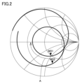
- FIG. 11 is a Smith chart of the antenna device for explaining impedance matching.
- FIG. 2 is a circuit diagram of an antenna device of Comparative Example 1.
- 4 is a graph showing reactance characteristics of the electronic component according to the first embodiment. 4 is a graph showing inductance characteristics of the electronic component according to the first embodiment.
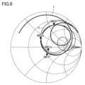
- FIG. 2 is a diagram showing a Smith chart of the antenna device according to the first embodiment.
- 5A and 5B are diagrams illustrating a return loss of the antenna device according to the first embodiment.
- FIG. 4 is a circuit diagram of an antenna device of Comparative Example 2.
- 13 is a graph showing reactance characteristics of an electronic component of Comparative Example 2.
- FIG. 11 is a circuit diagram of an antenna device of Comparative Example 3. FIG.
- FIG. 13 is a Smith chart of the antenna device according to Comparative Example 3.
- FIG. 11 is a diagram showing the return loss of the antenna device according to Comparative Example 3.
- FIG. 11 is a circuit diagram of an antenna device according to a second embodiment.
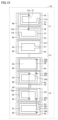
- FIG. 11 is an exploded plan view showing the structure of an electronic component according to a second embodiment.
- FIG. 11 is an exploded plan view showing a structure of an electronic component according to another embodiment.
- FIG. 11 is a circuit diagram of an antenna device according to a third embodiment.
- Fig. 1 is a circuit diagram of an antenna device 100 according to the first embodiment.
- the antenna device 100 includes a radiating element 20, a power supply circuit 30 that supplies power to the radiating element 20, and an electronic component 10 for matching the impedance between the power supply circuit 30 and the radiating element 20.
- the antenna device 100 is an antenna device capable of communication in a frequency range including, for example, 1 GHz to 5 GHz, and is built into a notebook computer, a mobile phone, a smartphone, a tablet, or the like.
- the antenna device 100 uses the electronic component 10 to match the impedance between the feed circuit 30 and the radiating element 20. Before describing the impedance matching of the antenna device 100 using the electronic component 10, the impedance matching of the antenna device not using the electronic component 10 will be described.
- Fig. 2 is a diagram showing a Smith chart of the antenna device for explaining impedance matching. Fig. 2 shows the Smith chart of the antenna device not using the electronic component 10.
- the Smith chart shown in Figure 2 has target frequency lines drawn from 0.1 GHz to 7 GHz. If you want to match the impedance at the frequencies of mark M01 (approximately 1.0 GHz) and mark M02 (approximately 4.0 GHz) in an antenna device, you need to move marks M01 and M02 in the direction of arrow A and adjust the inductance so that marks M01 and M02 are located near the horizontal line.
- FIG. 3 is a circuit diagram of antenna device 200 of comparison 1.
- the inductance is adjusted by connecting coil L1, which is an inductor, in series with power supply circuit 30 and radiating element 20.
- an electronic component 10 having a configuration as shown in FIG. 1 is adopted to match the impedance between the power supply circuit 30 and the radiating element 20.
- the electronic component 10 includes a first terminal P1, a second terminal P2, a coil L1 (first coil) connected in series between the first terminal P1 and the second terminal P2, a coil L2 (second coil) magnetically coupled to the coil L1, and a capacitor C1 (first capacitor) electrically connected in parallel to the coil L2.
- the coil L1 is electrically connected directly to one end of the coil L2 (connected by wiring), but is not electrically connected directly to the other end of the coil L2 (not connected by wiring).
- the coil L1 and the coil L2 are differentially connected, and the coupling coefficient between the coil L1 and the coil L2 is k. Note that even if the connection polarity between the coil L1 and the coil L2 is switched and the coil L1 and the coil L2 are connected in a additive manner, the reactance characteristic and the inductance characteristic of the electronic component 10 do not change.
- Electronic component 10 has a resonant circuit with resonant frequency f1, consisting of coil L2 and capacitor C1, as a parallel circuit to coil L1, and magnetically couples coil L1 and coil L2. Therefore, electronic component 10 has a characteristic in which inductance Lhi is smaller in a frequency range f3 (>f1) higher than resonant frequency f1 than inductance Llow in a frequency range f2 ( ⁇ f1) lower than resonant frequency f1 (Llow>Lhi).
- FIG. 4 is a graph showing the reactance characteristics of the electronic component 10 according to the first embodiment.
- FIG. 5 is a graph showing the inductance characteristics of the electronic component 10 according to the first embodiment.
- the reactance characteristics of the electronic component 10 are calculated by determining the imaginary part of the Z11 parameter of the Z parameter when the first terminal P1 is connected to the input port and the second terminal P2 is connected to ground (GND).
- FIG. 4 also shows graph b showing the reactance characteristics of coil L1 alone.
- the resonant frequency f1 of electronic component 10 is approximately 2.4 GHz, and at mark M01 (approximately 1.0 GHz), which is a frequency lower than resonant frequency f1, the reactance of electronic component 10 and the reactance of coil L1 alone are approximately the same. However, at mark M02 (approximately 4.0 GHz), which is a frequency higher than resonant frequency f1, the reactance of electronic component 10 is lower than the reactance of coil L1 alone. Note that the reactance of electronic component 10 and the reactance of coil L1 alone both tend to increase as the frequency increases.
- FIG. 5 also shows graph d showing the inductance characteristics of coil L1 alone.
- M01 approximately 1.0 GHz
- M02 approximately 4.0 GHz
- graph d showing the inductance characteristics of coil L1 alone is a constant value regardless of frequency.
- the inductance characteristic of the electronic component 10 is smaller than the inductance of the coil L1 alone in a frequency range higher than the resonant frequency f1. Therefore, the antenna device 100 can use the inductance characteristic of the electronic component 10 to match the impedance between the power supply circuit 30 and the radiating element 20 in multiple frequency ranges.
- the electronic component 10 may also be used as an element for matching impedance in high-frequency circuits other than the antenna device, such as RF (Radio Frequency) circuits, by utilizing the inductance characteristic of the electronic component 10.
- FIG. 6 is a diagram showing a Smith chart of the antenna device 100 according to the first embodiment.
- Figure 7 is a diagram showing the return loss of the antenna device 100 according to the first embodiment.
- the Smith chart shown in FIG. 6 shows target frequency lines from 0.1 GHz to 7 GHz.
- FIG. 6 also shows line f of antenna device 200 using coil L1 alone.
- mark M01e approximately 1.0 GHz
- mark M02e approximately 4.0 GHz
- the impedance of mark M02e is approximately 33.8+j14.7 ⁇
- the impedance of mark M02f is approximately 31.5+j62.3 ⁇ , meaning that mark M02e has a smaller imaginary part and is better matched.
- the reflection loss g of the antenna device 100 is smaller than the reflection loss h of the antenna device 200 at mark M02 (approximately 4.0 GHz). Therefore, it can be seen that the impedance of the antenna device 100 is better matched than that of the antenna device 200 in the frequency range of approximately 4.0 GHz.
- the horizontal axis is frequency and the vertical axis is reflection loss (return loss).
- the reflection loss is the reflection coefficient of the antenna devices 100, 200 when the electronic component 10 or coil L1 alone is viewed from the power supply circuit 30 in FIG. 1 or FIG. 3.
- inductance matching is performed using the electronic component 10, so even if it is matched to the impedance at low frequencies, low impedance can be achieved at high frequencies, and the impedance between the power supply circuit 30 and the radiating element 20 can be matched at both low and high frequencies.
- the electronic component 10 has a characteristic that the inductance Lhi in a frequency range f3 higher than the resonant frequency f1 is smaller than the inductance Llow in a frequency range f2 lower than the resonant frequency f1 (Llow>Lhi) by magnetically coupling the coil L1 and the coil L2.
- the fact that magnetically coupling the coil L1 and the coil L2 is an essential configuration of the electronic component 10 will be explained using an antenna device of comparative example 2.
- FIG. 8 is a circuit diagram of the antenna device 200a of comparative example 2.
- the antenna device 200a matches the impedance of the power supply circuit 30 and the radiating element 20 using the electronic component 12.
- the electronic component 12 includes a first terminal P1, a second terminal P2, a coil L1 connected in series between the first terminal P1 and the second terminal P2, a coil L2 that is not magnetically coupled to the coil L1, and a capacitor C1 electrically connected in parallel to the coil L2. Furthermore, in electronic component 12, coil L1 is electrically connected directly to one end of coil L2, but is not electrically connected directly to the other end of coil L2.
- Figure 9 is a graph showing the reactance characteristics of electronic component 12 of comparison 2.
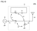
- FIG. 10 is a circuit diagram of an antenna device 200b of Comparative Example 3.
- the antenna device 200b uses an electronic component 13 to match the impedance of the power supply circuit 30 and the radiating element 20.
- the electronic component 13 includes a first terminal P1, a second terminal P2, a coil L1 connected in series between the first terminal P1 and the second terminal P2, a coil L3 shunt-connected to the wiring connecting the first terminal P1 and the second terminal P2, a coil L2 that is magnetically coupled to the coil L1 and the coil L3, and a capacitor C1 that is electrically connected in parallel to the coil L2. Furthermore, the coil L1 and the coil L3 of the electronic component 13 are not electrically connected directly to the coil L2.
- the electronic component 13 has a resonant circuit with a resonant frequency f1, which is made up of the coil L2 and the capacitor C1, as a parallel circuit to the coil L1, and the coils L1 and L2 are magnetically coupled.
- the electronic component 13 changes the impedance of the antenna device 200b because the coil L3 is shunt-connected to the radiating element 20. Specifically, because the coil L3 is shunt-connected, it moves counterclockwise on the locus of the admittance chart, and if it moves to the upper half of the Smith chart, it will move away from the center (50 ⁇ ) of the Smith chart due to the inductance components of the coils L1, L2, and the capacitor C1, making impedance matching difficult. Therefore, it is difficult for the antenna device 200b using the electronic component 13 to match the impedance of the power supply circuit 30 and the radiating element 20 in the required multiple frequency ranges.
- the Smith chart shown in FIG. 11 shows target frequency lines from 0.1 GHz to 7 GHz.
- FIG. 11 also shows line e of antenna device 100 using electronic component 10.
- Line k of antenna device 200b is far away from the horizontal line at the position of mark M01k (approximately 1.0 GHz), and the real part of mark M02k (approximately 4.0 GHz) is greater than 50 ⁇ .
- the impedance of mark M02e is approximately 33.78+j14.7 ⁇
- the impedance of mark M02k is approximately 214.32-j21.5 ⁇ .
- the real part of mark M02e has a value of approximately 33.78 ⁇ , while the real part of mark M02k has a value of approximately 214.32 ⁇ , which is large, and matching is not possible.
- the impedance of the antenna device 200b is significantly different, and the reflection loss m of the antenna device 200b is greater than the reflection loss g of the antenna device 100 at mark M02 (approximately 4.0 GHz). Therefore, it can be seen that the impedance of the antenna device 200b is not matched like that of the antenna device 100 in the frequency range of approximately 4.0 GHz. Note that in FIG. 12, the horizontal axis is frequency and the vertical axis is reflection loss (return loss).
- the antenna device 100 is able to keep the reflection loss low at mark M01 (approximately 1.0 GHz) and mark M02 (approximately 4.0 GHz), so it can be seen that the impedance of the power supply circuit 30 and the radiating element 20 is matched at both low and high frequencies.
- FIG. 13 is a circuit diagram of an antenna device 100a according to the second embodiment.
- the antenna device 100a includes a radiating element 20, a power supply circuit 30 that supplies power to the radiating element 20, and an electronic component 10a for matching the impedance between the power supply circuit 30 and the radiating element 20.
- the electronic component 10a includes a first terminal P1, a second terminal P2, a coil L1 (first coil) connected in series between the first terminal P1 and the second terminal P2, a coil L2 (second coil) that magnetically couples with the coil L1, and a capacitor C1 that is electrically connected in parallel with the coil L2. Furthermore, in the electronic component 10a, the coil L1 is not directly electrically connected to the coil L2 (not connected by wiring). Here, the coils L1 and L2 are differentially connected, and the coupling coefficient between the coils L1 and L2 is k. Note that even if the connection polarity of the coils L1 and L2 is swapped and the coils L1 and L2 are connected in a additive manner, there is no change in the reactance characteristic and inductance characteristic of the electronic component 10a.
- the reactance and inductance characteristics of electronic component 10a are approximately the same as those of electronic component 10.
- electronic component 10a has a characteristic in which inductance Lhi in a frequency range f3 (>f1) higher than resonance frequency f1 is smaller than inductance Llow in a frequency range f2 ( ⁇ f1) lower than resonance frequency f1 (Llow>Lhi). Therefore, the inductance characteristic of electronic component 10a is smaller than the inductance of coil L1 alone in a frequency range higher than resonance frequency f1, so that antenna device 100a can use the inductance characteristic of electronic component 10a to match the impedance of power supply circuit 30 and radiating element 20 in multiple frequency ranges.
- electronic component 10a can match the impedance between power supply circuit 30 and radiating element 20 in multiple frequency ranges, and has almost the same inductance characteristics, but has a different structure.
- Electronic component 10a can be configured as a rectangular parallelepiped chip component that contains coil L1, coil L2, and capacitor C1.
- FIG 14 is an exploded plan view showing the structure of electronic component 10a according to embodiment 2.
- Electronic component 10a is composed of an insulator (ceramic element body) made by stacking multiple substrates (ceramic green sheets) on which the wiring of the coil and capacitor shown in Figure 14 is formed.
- the insulator has a pair of opposing main surfaces and a side surface connecting the main surfaces.
- Multiple conductor patterns 1a, 1b, 2a-2c and multiple electrode patterns 5a, 5b are stacked parallel to the main surface of insulator 1 to form electronic component 10a containing coil L1, coil L2, and capacitor C1.
- the conductor patterns 1a, 1b, 2a-2c, the wiring patterns 11a, 11b, 51, and the electrode patterns 5a, 5b are each formed on the insulating substrates 3a-3g by a printing method.
- the electronic component 10a is formed by stacking the insulating substrates 3a-3g on which the conductor patterns 1a, 1b, 2a-2c, etc. are formed.
- a conductor pattern 1a that constitutes part of the coil L1 is formed on the insulating substrate 3a.
- the conductor pattern 1a is formed so as to go around approximately 3/4 of the way around the insulating substrate 3a clockwise from the right side in the figure.
- the starting end of the conductor pattern 1a is electrically connected to the external electrode 4a via the wiring pattern 11a.
- the external electrode 4a corresponds to the first terminal P1 shown in FIG. 1, for example.
- a connection portion 31a that connects to the via conductor 31 is provided near the end of the conductor pattern 1a.
- a conductor pattern 1b that constitutes part of coil L1 is formed on insulating substrate 3b.
- Conductor pattern 1b is formed so as to go around approximately 3/4 of the way around clockwise from the center of insulating substrate 3b in the figure.
- a connection portion 31b that connects to via conductor 31 is provided near the starting end of conductor pattern 1b.
- the end of conductor pattern 1b is electrically connected to external electrode 4b through wiring pattern 11b.
- External electrode 4b corresponds to, for example, second terminal P2 shown in FIG. 1.
- Coil L1 is formed of approximately 1.5 turns of coil by connecting conductor patterns 1a and 1b with via conductor 31.
- An electrode pattern 5a that constitutes one electrode (first electrode) of the capacitor C1 is formed on the insulating substrate 3c.
- the electrode pattern 5a When viewed in a plan view from the stacking direction, the electrode pattern 5a is provided in an area that partially overlaps with the openings of the coils L1 and L2.
- the electrode pattern 5a may be provided in a position that does not overlap with the openings of the coils L1 and L2, thereby realizing the electronic component 10a without interfering with the magnetic field generated by the coils L1 and L2.
- the electrode pattern 5a has a connection portion 36a that connects to the via conductor 36.
- the insulating substrate 3d is provided with an electrode pattern 5b that constitutes one electrode (second electrode) of the capacitor C1.
- the electrode pattern 5b is provided at a position that overlaps with the electrode pattern 5a formed on the insulating substrate 3c.
- the area of the electrode pattern 5b is larger than that of the electrode pattern 5a.
- the area of the electrode pattern 5a may be larger than that of the electrode pattern 5b.
- a connection portion 32a that connects to the via conductor 32 is provided near one end of the electrode pattern 5b.
- the insulating substrate 3d is provided with a connection portion 36b that connects to the via conductor 36 at a position where the electrode pattern 5b is not provided.
- the capacitor C1 is composed of the electrode pattern 5a and the electrode pattern 5b, but multiple insulating substrates are stacked between the insulating substrate 3c and the insulating substrate 3d.
- An electrode that overlaps with the electrode patterns 5a and 5b when viewed from above in the stacking direction may be provided as a floating electrode on the insulating substrate stacked between the insulating substrate 3c and the insulating substrate 3d.
- a conductor pattern 2a that constitutes part of coil L2 is formed on insulating substrate 3e.
- Conductor pattern 2a is formed so as to wrap around insulating substrate 3e counterclockwise from the upper right side in the figure.
- a connection portion 32b that connects to via conductor 32 is provided near the start end of conductor pattern 2a.
- a connection portion 33a that connects to via conductor 33 is provided near the end end of conductor pattern 2a.
- a connection portion 36c that connects to via conductor 36 is provided on insulating substrate 3e at a position where conductor pattern 2a is not provided.
- a conductor pattern 2b constituting part of the coil L2 is formed on the insulating substrate 3f.
- the conductor pattern 2b is formed so as to go around the insulating substrate 3f counterclockwise from the upper right side in the figure.
- a connection portion 34a that connects to the via conductor 34 is provided near the start end of the conductor pattern 2b.
- a connection portion 35a that connects to the via conductor 35 is provided near the end end of the conductor pattern 2b.
- a connection portion 36d that connects to the via conductor 36 is provided on the insulating substrate 3f at a position where the conductor pattern 2b is not provided. Note that, between the insulating substrate 3e and the insulating substrate 3f, a plurality of insulating substrates on which conductor patterns that constitute part of the coil L2 are formed are provided, but are not shown in the figure.
- a conductor pattern 2c that constitutes part of coil L2 is formed on insulating substrate 3g.
- Conductor pattern 2c is formed so as to go counterclockwise around approximately 3/4 of the way around insulating substrate 3g from the upper right side in the figure.
- a connection portion 35b that connects to via conductor 35 is provided near the start end of conductor pattern 2c.
- a connection portion 36e that connects to via conductor 36 is provided near the end end of conductor pattern 2c.
- Coil L2 is formed as a multiple-turn coil by connecting conductor patterns 2a to 2c with via conductors 33 to 35.
- FIG. 15 is an exploded plan view showing the structure of electronic component 10 according to another embodiment. Note that in the exploded plan view showing the structure of electronic component 10, the same components as those in the exploded plan view showing the structure of electronic component 10a shown in FIG. 14 are designated by the same reference numerals and detailed descriptions will not be repeated.
- An electrode pattern 5a that constitutes one electrode (first electrode) of the capacitor C1 is formed on the insulating substrate 3c1.
- the electrode pattern 5a When viewed in a plan view from the stacking direction, the electrode pattern 5a is provided in an area that partially overlaps with the openings of the coils L1 and L2.
- the electrode pattern 5a may be provided in a position that does not overlap with the openings of the coils L1 and L2, thereby realizing the electronic component 10 without interfering with the magnetic field generated by the coils L1 and L2.
- One end of the electrode pattern 5a is electrically connected to the external electrode 4a via the wiring pattern 51.
- the insulating substrate 3d1 is provided with an electrode pattern 5b that constitutes one electrode (second electrode) of the capacitor C1.
- the electrode pattern 5b When viewed from above in the stacking direction, the electrode pattern 5b is provided at a position that overlaps with the electrode pattern 5a formed on the insulating substrate 3c1.
- the area of the electrode pattern 5b is larger than that of the electrode pattern 5a.
- the area of the electrode pattern 5a may be larger than that of the electrode pattern 5b.
- a connection portion 32a that connects to the via conductor 32 is provided near one end of the electrode pattern 5b.
- the capacitor C1 is composed of the electrode pattern 5a and the electrode pattern 5b, but multiple insulating substrates are stacked between the insulating substrate 3c1 and the insulating substrate 3d1.
- An electrode that overlaps with the electrode patterns 5a and 5b when viewed from above in the stacking direction may be provided as a floating electrode on the insulating substrate stacked between the insulating substrate 3c1 and the insulating
- a conductor pattern 2a that constitutes part of coil L2 is formed on insulating substrate 3e1.
- Conductor pattern 2a is formed so as to make approximately one full turn clockwise from the upper right side of insulating substrate 3e1 in the figure.
- a connection portion 32b that connects to via conductor 32 is provided near the starting end of conductor pattern 2a.
- a connection portion 33a that connects to via conductor 33 is provided near the end of conductor pattern 2a.
- a conductor pattern 2b constituting part of coil L2 is formed on insulating substrate 3f1.
- Conductor pattern 2b is formed so as to make approximately one revolution on insulating substrate 3f1.
- a connection portion 34a that connects to via conductor 34 is provided near the beginning of conductor pattern 2b.
- a connection portion 35a that connects to via conductor 35 is provided near the end of conductor pattern 2b. Note that, between insulating substrate 3e1 and insulating substrate 3f1, multiple insulating substrates on which conductor patterns that form part of coil L2 are formed are provided, but are not shown in the figure.
- a conductor pattern 2c that constitutes part of the coil L2 is formed on the insulating substrate 3g1.
- the conductor pattern 2c is formed so as to occupy approximately 3/4 of the circumference of the insulating substrate 3g1.
- a connection portion 35b that connects to the via conductor 35 is provided near the starting end of the conductor pattern 2c. The end of the conductor pattern 2c is electrically connected to the external electrode 4a via the wiring pattern 21c.
- the electronic component 10 is configured as shown in FIG. 15, so that one end of the coil L2 is connected to the external electrode 4a. Therefore, the wiring pattern 21c is formed as an extraction wiring for connecting the conductor pattern 2c of the coil L2 to the external electrode 4a, so that the wiring pattern 21c can also be used as the inductance of the coil L2, and the electronic component 10 can be made smaller.
- Fig. 16 is a circuit diagram of an antenna device 100b according to the third embodiment.
- the antenna device 100b includes a radiating element 20, a power supply circuit 30 that supplies power to the radiating element 20, and an electronic component 10b for matching the impedance between the power supply circuit 30 and the radiating element 20.
- the electronic component 10b includes a first terminal P1 electrically connected to the wiring 25 that connects the radiating element 20 and the power supply circuit 30, a second terminal P2 electrically connected to the ground (GND), a coil L1 (first coil) connected in series between the first terminal P1 and the second terminal P2, a coil L2 (second coil) that magnetically couples with the coil L1, and a capacitor C1 electrically connected in parallel with the coil L2.
- the coil L1 is electrically connected directly to one end of the coil L2, but is not electrically connected directly to the other end of the coil L2.
- the coil L1 does not necessarily have to be electrically connected to the coil L2.
- the antenna device 100b can match the impedance between the power supply circuit 30 and the radiating element 20 by shunt-connecting the electronic component 10b to the wiring 25 that connects the radiating element 20 and the power supply circuit 30. Furthermore, the antenna device 100b can be considered an inverted-F antenna (IFA) because the wiring 25 is connected to ground (GND) via the electronic component 10b, and the electronic component 10b also functions as a short-circuit point.
- IFA inverted-F antenna
- the antenna device 100 according to the first embodiment employs an electronic component 10 including a capacitor C1 (first capacitor) electrically connected in parallel with the coil L2 as shown in Fig. 1.
- the capacitor included in the electronic component 10 is not limited to the capacitor C1.
- the antenna device according to the fourth embodiment employs an electronic component including a capacitor electrically connected in parallel with the coil L2.
- Fig. 17 is a circuit diagram of an antenna device 100c according to the fourth embodiment.
- the antenna device 100c uses the electronic component 10c to match the impedance between the power supply circuit 30 and the radiating element 20.
- the electronic component 10c includes a first terminal P1, a second terminal P2, a coil L1 (first coil) connected in series between the first terminal P1 and the second terminal P2, a capacitor C2 (second capacitor) electrically connected in parallel with the coil L1, a coil L2 (second coil) that magnetically couples with the coil L1, and a capacitor C1 electrically connected in parallel with the coil L2.
- the coil L1 is electrically connected directly to one end of the coil L2 (connected by wiring), but is not electrically connected directly to the other end of the coil L2 (not connected by wiring).
- the coil L1 and the coil L2 are differentially connected, and the coupling coefficient between the coil L1 and the coil L2 is k. Furthermore, even if the connection polarity of coil L1 and coil L2 is swapped and coil L1 and coil L2 are connected in a additive manner, there is no change in the reactance and inductance characteristics of electronic component 10c.
- Electronic component 10c has a resonant circuit with resonant frequency f1, consisting of coil L2 and capacitor C1, as a parallel circuit to coil L1, and furthermore, capacitor C2 is connected in parallel to coil L1. Therefore, electronic component 10c can make the reactance characteristic negative (capacitive) in the frequency range f3 (>f1) higher than resonant frequency f1 (especially 3 GHz or higher), and there is no need to add another capacitor to obtain new matching in the high frequency range f3.
- Figure 18 is a graph showing the reactance characteristics of electronic component 10c according to embodiment 4.
- Figure 18 shows a graph showing the reactance characteristics of electronic component 10c. It can be seen from Figure 18 that the reactance characteristics are negative (capacitive) in the frequency range higher than 3 GHz.
- the configuration in which the capacitor C2 is connected in parallel to the coil L1 may be applied to the antenna device 100a shown in FIG. 13 and the antenna device 100b shown in FIG. 16.
- An antenna device A power supply circuit; A radiating element connected to a feeding circuit; an electronic component arranged between the power supply circuit and the radiating element for matching impedance between the power supply circuit and the radiating element; Electronic components are A first terminal; A second terminal; a first coil connected in series between the first terminal and the second terminal; A second coil that is magnetically coupled to the first coil; A first capacitor electrically connected in parallel with the second coil.
- the antenna device includes an electronic component that includes a second coil that is magnetically coupled to a first coil that is connected in series to a first terminal and a second terminal, and a first capacitor that is electrically connected in parallel to the second coil, and therefore it is possible to match the impedance of the power supply circuit and the impedance of the radiating element in multiple frequency ranges.
- the resonant frequency of the parallel circuit including the second coil and the first capacitor is a frequency that is between the multiple resonant frequencies of the radiating element.
- the antenna device according to (1) or (2), The first coil is directly electrically connected to one end of the second coil, but is not directly electrically connected to the other end of the second coil.
- the antenna device according to (1) or (2), The first coil is not directly electrically connected to the second coil.
- the antenna device has a first terminal electrically connected to the feeding circuit and a second terminal electrically connected to the radiating element.
- the antenna device has a first terminal electrically connected between the feeding circuit and the radiating element, and a second terminal electrically connected to the ground electrode.
- the antenna device according to any one of (1) to (6),
- the power supply further includes a second capacitor electrically connected in parallel with the first coil.
- An electronic component according to the present disclosure is an electronic component for matching impedance between a feed circuit and a radiating element in an antenna device, A first terminal; A second terminal; a first coil connected in series between the first terminal and the second terminal; A second coil that is magnetically coupled to the first coil; A first capacitor electrically connected in parallel with the second coil.
- the electronic component disclosed herein includes a second coil that is magnetically coupled to a first coil that is connected in series to a first terminal and a second terminal, and a first capacitor that is electrically connected in parallel to the second coil, so that the impedance of the power supply circuit of the antenna device can be matched with the impedance of the radiating element in multiple frequency ranges.
- the electronic component according to (8), The first coil is directly electrically connected to one end of the second coil, but is not directly electrically connected to the other end of the second coil.
- the power supply further includes a second capacitor electrically connected in parallel with the first coil.
- 1a, 1b, 2a to 2c conductor patterns
- 3a to 3g insulating substrate
- 4a, 4b external electrodes
- 5a, 5b electrode patterns
- 10, 10a, 10b electronic components
- 11a, 11b, 21c 51: wiring patterns
- 20 radiating elements
- 30 power supply circuits
- 31 to 36 via conductors
- 100, 100a, 100b antenna devices.
Landscapes
- Engineering & Computer Science (AREA)
- Power Engineering (AREA)
- Details Of Aerials (AREA)
Priority Applications (3)
| Application Number | Priority Date | Filing Date | Title |
|---|---|---|---|
| CN202480031372.2A CN121079848A (zh) | 2023-05-29 | 2024-01-29 | 天线装置以及电子部件 |
| JP2025523255A JPWO2024247363A1 (https=) | 2023-05-29 | 2024-01-29 | |
| US19/336,567 US20260018791A1 (en) | 2023-05-29 | 2025-09-23 | Antenna device, electronic component and associated methods |
Applications Claiming Priority (2)
| Application Number | Priority Date | Filing Date | Title |
|---|---|---|---|
| JP2023-087852 | 2023-05-29 | ||
| JP2023087852 | 2023-05-29 |
Related Child Applications (1)
| Application Number | Title | Priority Date | Filing Date |
|---|---|---|---|
| US19/336,567 Continuation US20260018791A1 (en) | 2023-05-29 | 2025-09-23 | Antenna device, electronic component and associated methods |
Publications (1)
| Publication Number | Publication Date |
|---|---|
| WO2024247363A1 true WO2024247363A1 (ja) | 2024-12-05 |
Family
ID=93657650
Family Applications (1)
| Application Number | Title | Priority Date | Filing Date |
|---|---|---|---|
| PCT/JP2024/002586 Ceased WO2024247363A1 (ja) | 2023-05-29 | 2024-01-29 | アンテナ装置、および電子部品 |
Country Status (4)
| Country | Link |
|---|---|
| US (1) | US20260018791A1 (https=) |
| JP (1) | JPWO2024247363A1 (https=) |
| CN (1) | CN121079848A (https=) |
| WO (1) | WO2024247363A1 (https=) |
Citations (3)
| Publication number | Priority date | Publication date | Assignee | Title |
|---|---|---|---|---|
| WO2015178204A1 (ja) * | 2014-05-19 | 2015-11-26 | 株式会社村田製作所 | アンテナ整合回路、アンテナ整合モジュール、アンテナ装置および無線通信装置 |
| JP2016152621A (ja) * | 2015-02-17 | 2016-08-22 | ジョインセット株式会社 | アンテナ帯域幅拡張装置 |
| WO2018101284A1 (ja) * | 2016-11-29 | 2018-06-07 | 株式会社村田製作所 | アンテナ装置および電子機器 |
Family Cites Families (2)
| Publication number | Priority date | Publication date | Assignee | Title |
|---|---|---|---|---|
| US10020793B2 (en) * | 2015-01-21 | 2018-07-10 | Qualcomm Incorporated | Integrated filters in output match elements |
| JP6908202B2 (ja) * | 2018-12-14 | 2021-07-21 | 株式会社村田製作所 | 整合回路、整合回路素子及び通信装置 |
-
2024
- 2024-01-29 CN CN202480031372.2A patent/CN121079848A/zh active Pending
- 2024-01-29 JP JP2025523255A patent/JPWO2024247363A1/ja active Pending
- 2024-01-29 WO PCT/JP2024/002586 patent/WO2024247363A1/ja not_active Ceased
-
2025
- 2025-09-23 US US19/336,567 patent/US20260018791A1/en active Pending
Patent Citations (3)
| Publication number | Priority date | Publication date | Assignee | Title |
|---|---|---|---|---|
| WO2015178204A1 (ja) * | 2014-05-19 | 2015-11-26 | 株式会社村田製作所 | アンテナ整合回路、アンテナ整合モジュール、アンテナ装置および無線通信装置 |
| JP2016152621A (ja) * | 2015-02-17 | 2016-08-22 | ジョインセット株式会社 | アンテナ帯域幅拡張装置 |
| WO2018101284A1 (ja) * | 2016-11-29 | 2018-06-07 | 株式会社村田製作所 | アンテナ装置および電子機器 |
Also Published As
| Publication number | Publication date |
|---|---|
| US20260018791A1 (en) | 2026-01-15 |
| JPWO2024247363A1 (https=) | 2024-12-05 |
| CN121079848A (zh) | 2025-12-05 |
Similar Documents
| Publication | Publication Date | Title |
|---|---|---|
| JP6614363B2 (ja) | アンテナ装置および電子機器 | |
| CN102484497B (zh) | 稳频电路、天线装置、及通信终端设备 | |
| CN103141031B (zh) | 阻抗变换电路以及通信终端装置 | |
| US9692099B2 (en) | Antenna-matching device, antenna device and mobile communication terminal | |
| US10277192B2 (en) | Phase shifter, impedance matching circuit, and communication terminal apparatus | |
| JP6838631B2 (ja) | アンテナ装置および通信端末装置 | |
| CN206506500U (zh) | 变压器型移相器、移相电路以及通信终端装置 | |
| US9287629B2 (en) | Impedance conversion device, antenna device and communication terminal device | |
| WO2018101285A1 (ja) | 磁界結合素子、アンテナ装置および電子機器 | |
| CN104704678A (zh) | 阻抗转换电路的设计方法 | |
| US10348266B2 (en) | Impedance conversion circuit, antenna apparatus, and wireless communication apparatus | |
| US8797225B2 (en) | Antenna device and communication terminal apparatus | |
| US20240235516A1 (en) | Filter device, antenna device, and antenna module | |
| US20090109106A1 (en) | Surface-mount antenna and antenna device | |
| WO2024247363A1 (ja) | アンテナ装置、および電子部品 | |
| TW202005175A (zh) | 多頻天線裝置 |
Legal Events
| Date | Code | Title | Description |
|---|---|---|---|
| 121 | Ep: the epo has been informed by wipo that ep was designated in this application |
Ref document number: 24814850 Country of ref document: EP Kind code of ref document: A1 |
|
| ENP | Entry into the national phase |
Ref document number: 2025523255 Country of ref document: JP Kind code of ref document: A |
|
| WWE | Wipo information: entry into national phase |
Ref document number: 2025523255 Country of ref document: JP |
|
| NENP | Non-entry into the national phase |
Ref country code: DE |