WO2024246720A1 - 光学機器および電子機器 - Google Patents
光学機器および電子機器 Download PDFInfo
- Publication number
- WO2024246720A1 WO2024246720A1 PCT/IB2024/055125 IB2024055125W WO2024246720A1 WO 2024246720 A1 WO2024246720 A1 WO 2024246720A1 IB 2024055125 W IB2024055125 W IB 2024055125W WO 2024246720 A1 WO2024246720 A1 WO 2024246720A1
- Authority
- WO
- WIPO (PCT)
- Prior art keywords
- light
- layer
- optical path
- optical
- transistor
- Prior art date
- Legal status (The legal status is an assumption and is not a legal conclusion. Google has not performed a legal analysis and makes no representation as to the accuracy of the status listed.)
- Ceased
Links
Images
















Classifications
-
- G—PHYSICS
- G02—OPTICS
- G02B—OPTICAL ELEMENTS, SYSTEMS OR APPARATUS
- G02B27/00—Optical systems or apparatus not provided for by any of the groups G02B1/00 - G02B26/00, G02B30/00
- G02B27/28—Optical systems or apparatus not provided for by any of the groups G02B1/00 - G02B26/00, G02B30/00 for polarising
- G02B27/286—Optical systems or apparatus not provided for by any of the groups G02B1/00 - G02B26/00, G02B30/00 for polarising for controlling or changing the state of polarisation, e.g. transforming one polarisation state into another
-
- G—PHYSICS
- G02—OPTICS
- G02B—OPTICAL ELEMENTS, SYSTEMS OR APPARATUS
- G02B27/00—Optical systems or apparatus not provided for by any of the groups G02B1/00 - G02B26/00, G02B30/00
- G02B27/01—Head-up displays
- G02B27/017—Head mounted
- G02B27/0172—Head mounted characterised by optical features
-
- G—PHYSICS
- G02—OPTICS
- G02B—OPTICAL ELEMENTS, SYSTEMS OR APPARATUS
- G02B27/00—Optical systems or apparatus not provided for by any of the groups G02B1/00 - G02B26/00, G02B30/00
- G02B27/02—Viewing or reading apparatus
-
- G—PHYSICS
- G02—OPTICS
- G02B—OPTICAL ELEMENTS, SYSTEMS OR APPARATUS
- G02B27/00—Optical systems or apparatus not provided for by any of the groups G02B1/00 - G02B26/00, G02B30/00
- G02B27/02—Viewing or reading apparatus
- G02B27/022—Viewing apparatus
- G02B27/024—Viewing apparatus comprising a light source, e.g. for viewing photographic slides, X-ray transparancies
- G02B27/026—Viewing apparatus comprising a light source, e.g. for viewing photographic slides, X-ray transparancies and a display device, e.g. CRT, LCD, for adding markings or signs or to enhance the contrast of the viewed object
-
- G—PHYSICS
- G02—OPTICS
- G02B—OPTICAL ELEMENTS, SYSTEMS OR APPARATUS
- G02B27/00—Optical systems or apparatus not provided for by any of the groups G02B1/00 - G02B26/00, G02B30/00
- G02B27/10—Beam splitting or combining systems
- G02B27/14—Beam splitting or combining systems operating by reflection only
-
- G—PHYSICS
- G02—OPTICS
- G02B—OPTICAL ELEMENTS, SYSTEMS OR APPARATUS
- G02B27/00—Optical systems or apparatus not provided for by any of the groups G02B1/00 - G02B26/00, G02B30/00
- G02B27/28—Optical systems or apparatus not provided for by any of the groups G02B1/00 - G02B26/00, G02B30/00 for polarising
- G02B27/288—Filters employing polarising elements, e.g. Lyot or Solc filters
-
- G—PHYSICS
- G02—OPTICS
- G02B—OPTICAL ELEMENTS, SYSTEMS OR APPARATUS
- G02B5/00—Optical elements other than lenses
-
- G—PHYSICS
- G02—OPTICS
- G02B—OPTICAL ELEMENTS, SYSTEMS OR APPARATUS
- G02B5/00—Optical elements other than lenses
- G02B5/08—Mirrors
- G02B5/10—Mirrors with curved faces
-
- G—PHYSICS
- G02—OPTICS
- G02B—OPTICAL ELEMENTS, SYSTEMS OR APPARATUS
- G02B5/00—Optical elements other than lenses
- G02B5/30—Polarising elements
-
- G—PHYSICS
- G02—OPTICS
- G02B—OPTICAL ELEMENTS, SYSTEMS OR APPARATUS
- G02B5/00—Optical elements other than lenses
- G02B5/30—Polarising elements
- G02B5/3016—Polarising elements involving passive liquid crystal elements
-
- G—PHYSICS
- G02—OPTICS
- G02B—OPTICAL ELEMENTS, SYSTEMS OR APPARATUS
- G02B5/00—Optical elements other than lenses
- G02B5/30—Polarising elements
- G02B5/3083—Birefringent or phase retarding elements
-
- G—PHYSICS
- G09—EDUCATION; CRYPTOGRAPHY; DISPLAY; ADVERTISING; SEALS
- G09F—DISPLAYING; ADVERTISING; SIGNS; LABELS OR NAME-PLATES; SEALS
- G09F9/00—Indicating arrangements for variable information in which the information is built-up on a support by selection or combination of individual elements
-
- G—PHYSICS
- G09—EDUCATION; CRYPTOGRAPHY; DISPLAY; ADVERTISING; SEALS
- G09F—DISPLAYING; ADVERTISING; SIGNS; LABELS OR NAME-PLATES; SEALS
- G09F9/00—Indicating arrangements for variable information in which the information is built-up on a support by selection or combination of individual elements
- G09F9/30—Indicating arrangements for variable information in which the information is built-up on a support by selection or combination of individual elements in which the desired character or characters are formed by combining individual elements
-
- H—ELECTRICITY
- H10—SEMICONDUCTOR DEVICES; ELECTRIC SOLID-STATE DEVICES NOT OTHERWISE PROVIDED FOR
- H10K—ORGANIC ELECTRIC SOLID-STATE DEVICES
- H10K59/00—Integrated devices, or assemblies of multiple devices, comprising at least one organic light-emitting element covered by group H10K50/00
- H10K59/10—OLED displays
- H10K59/12—Active-matrix OLED [AMOLED] displays
-
- G—PHYSICS
- G02—OPTICS
- G02B—OPTICAL ELEMENTS, SYSTEMS OR APPARATUS
- G02B27/00—Optical systems or apparatus not provided for by any of the groups G02B1/00 - G02B26/00, G02B30/00
- G02B27/01—Head-up displays
- G02B27/017—Head mounted
- G02B2027/0178—Eyeglass type
Definitions
- One aspect of the present invention relates to an optical instrument.
- one aspect of the present invention is not limited to the above technical field.
- the technical field of one aspect of the invention disclosed in this specification relates to an object, a method, or a manufacturing method.
- one aspect of the present invention relates to a process, a machine, a manufacture, or a composition of matter. Therefore, more specifically, examples of the technical field of one aspect of the present invention disclosed in this specification include a semiconductor device, a display device, a liquid crystal display device, a light-emitting device, a lighting device, a power storage device, a memory device, an imaging device, an operation method thereof, or a manufacturing method thereof.
- a semiconductor device refers to any device that can function by utilizing semiconductor characteristics.
- a transistor and a semiconductor circuit are one embodiment of a semiconductor device.
- a memory device, a display device, an imaging device, and an electronic device may include a semiconductor device.
- Goggle-type and eyeglass-type devices are being developed as electronic devices for XR (a general term for virtual reality (VR), augmented reality (AR), mixed reality (MR), etc.).
- XR a general term for virtual reality (VR), augmented reality (AR), mixed reality (MR), etc.
- Display panels used in these electronic devices typically include display devices equipped with liquid crystal elements, organic EL (Electro Luminescence) elements, or display devices equipped with light-emitting diodes (LEDs: Light Emitting Diodes), etc.
- Display devices equipped with organic EL elements do not require the backlight required for liquid crystal display devices, so they are thin, lightweight, have high contrast, and can reduce power consumption.
- an example of a display device using organic EL elements is disclosed in Patent Document 1.
- Patent Document 2 discloses an example of a high-brightness display device suitable for goggle-type and eyeglass-type device applications, in which a microlens array is provided to increase the light extraction efficiency.
- Such glasses-type devices often use selective reflection optical devices that utilize polarized light.
- Selective reflection optical devices are becoming smaller and lighter, but because they use polarized light, they have the problem of low light utilization efficiency.
- one object of one embodiment of the present invention is to provide an optical device with good display visibility. Another object is to provide an optical device with high light utilization efficiency. Another object is to provide an electronic device that includes the optical device. Another object is to provide an electronic device that consumes low power. Another object is to provide a new electronic device.
- One aspect of the present invention relates to an optical device with high light utilization efficiency.
- One aspect of the present invention is an optical device having a first optical path, a second optical path, and a third optical path, the first optical path and the second optical path having a common starting point, the third optical path having a different starting point from the first optical path and the second optical path, the first to third optical paths merging at their respective end points, the light emitted from the end point of the first optical path and the light emitted from the end point of the third optical path being a first linearly polarized light, the light emitted from the end point of the second optical path being a second linearly polarized light, and the first linearly polarized light having a vibration direction perpendicular to that of the second linearly polarized light.
- a reflective polarizing plate, a first retardation plate, and a half mirror are provided on the first optical path, a reflective polarizing plate, a second retardation plate, and a mirror are provided on the second optical path, and a linear polarizing plate, a third retardation plate, a half mirror, a first retardation plate, and a reflective polarizing plate are provided on the third optical path, the starting point of the first optical path and the second optical path is the reflective polarizing plate, the starting point of the third optical path is the linear polarizing plate, and the end points of the first optical path to the third optical path are the reflective polarizing plate.
- Another aspect of the present invention is an optical device having a reflective polarizing plate, a first retardation plate, a second retardation plate, a third retardation plate, a linear polarizing plate, a half mirror, and a mirror, the reflective polarizing plate being arranged at an angle such that light traveling straight from the light source is obliquely incident, the first retardation plate, the half mirror, the second retardation plate, and the linear polarizing plate being arranged in this order from the reflective polarizing plate side in the direction in which the light reflected by the reflective polarizing plate travels, and the third retardation plate and the mirror being arranged in this order from the reflective polarizing plate side in the direction in which the light passing through the reflective polarizing plate travels.
- Another aspect of the present invention is an optical device having a reflective polarizing plate, a retardation plate, a linear polarizing plate, a half mirror, and a mirror, where the reflective polarizing plate is arranged at an angle such that light traveling in a straight line from a light source is obliquely incident, and the half mirror, retardation plate, and linear polarizing plate are arranged in this order from the reflective polarizing plate side in the direction in which the light reflected by the reflective polarizing plate travels, and the mirror is arranged in the direction in which the light passing through the reflective polarizing plate travels.
- the reflective polarizing plate can have cholesteric liquid crystal.
- the half mirror and mirror can have a curved surface that is concave on the reflective polarizer side.
- a lens may be provided between the light source and the reflective polarizer, or between the mirror and the reflective polarizer, or both.
- An electronic device having the above optical device and a display panel having an organic EL element as a light source is also an aspect of the present invention.
- an optical device having good display visibility can be provided.
- an optical device having high light utilization efficiency can be provided.
- an electronic device having the optical device can be provided.
- an electronic device with low power consumption can be provided.
- a new electronic device can be provided.
- FIG. 1 is a diagram illustrating an electronic device.
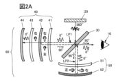
- 2A and 2B are diagrams illustrating an optical device.
- 3A and 3B are diagrams illustrating the light utilization efficiency in an optical device.
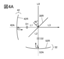
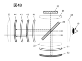
- 4A and 4B are diagrams illustrating an optical device.
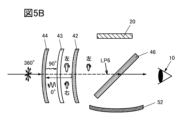
- 5A and 5B are diagrams illustrating an optical device.
- FIG. 6 is a diagram illustrating a reflector having cholesteric liquid crystal.
- 7A to 7E are diagrams illustrating a display panel.
- FIG. 8 is a diagram illustrating a glasses-type device.
- 9A to 9C are diagrams illustrating an example of the configuration of a display panel.
- 10A and 10B are diagrams illustrating an example of the configuration of a display panel.
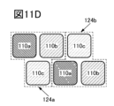
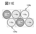
- 11A to 11F are diagrams for explaining examples of pixel configurations.
- FIGS. 12A and 12B are diagrams illustrating an example of the configuration of a display panel.
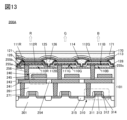
- FIG. 13 is a diagram illustrating an example of the configuration of a display panel.
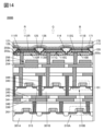
- FIG. 14 is a diagram illustrating an example of the configuration of a display panel.
- FIG. 15 is a diagram illustrating an example of the configuration of a display panel.
- FIG. 16 is a diagram illustrating an example of the configuration of a display panel.
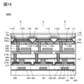
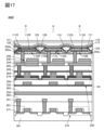
- FIG. 17 is a diagram illustrating an example of the configuration of a display panel.
- FIG. 18 is a diagram illustrating an example of the configuration of a display panel.
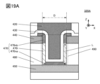
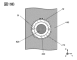
- 19A and 19B are diagrams illustrating a transistor.
- 20A and 20B are diagrams illustrating a transistor.
- an element may be composed of multiple elements as long as this does not cause any functional problems.
- multiple transistors that operate as switches may be connected in series or parallel.
- a capacitor may be divided and placed in multiple locations.
- one conductor may have multiple functions, such as wiring, an electrode, and a terminal, and in this specification, multiple names may be used for the same element. Even if elements are shown in a circuit diagram as being directly connected, in reality, the elements may be connected via one or more conductors, and in this specification, such configurations are also included in the category of direct connection.
- One aspect of the present invention is an electronic device, such as an optical see-through eyeglass-type device, and an optical device that can be used with the electronic device.
- the optical device has a first optical path, a second optical path, and a third optical path, and the first to third optical paths merge at the end points of each optical path.
- the first optical path and the second optical path are paths of light using the display panel as a light source
- the third optical path is a path of light using external light as a light source.
- the display of the display panel can be viewed as being superimposed on the external scene.
- a first linearly polarized light is emitted from the end point of the first optical path, and a second linearly polarized light is emitted from the end point of the second optical path.
- the vibration directions of the first linearly polarized light and the second linearly polarized light are perpendicular to each other. These polarized lights can be merged by using a reflective polarizing plate.
- the optical device of one embodiment of the present invention is configured to merge both the first optical path and the second optical path by the action of a reflective polarizer, and can increase the efficiency of use of light emitted by the display panel. By increasing the efficiency of light use of the optical device, it is possible to display with reduced brightness on the display panel, which can reduce power consumption and extend the life of the display device.
- Figure 1 is a perspective view illustrating an electronic device according to one embodiment of the present invention, showing a display panel and optical devices included in the electronic device. Note that the shapes of the elements shown in Figure 1 are examples.
- Optical device 60 has a reflective polarizer 30, an optical unit 40, and an optical unit 50.
- the reflective polarizer 30 is also an element that performs functions such as polarization conversion in combination with elements possessed by both optical unit 40 and optical unit 50. Therefore, it can also be said that the reflective polarizer 30 is an element of each of optical unit 40 and optical unit 50.
- the reflective polarizer 30 is flat and can be arranged at an angle such that light traveling straight from the display panel 20, which is the first light source, is obliquely incident on the reflective surface.
- the reflective polarizer 30 is arranged so that the angle of incidence of light emitted perpendicularly from the display surface of the display panel 20 is greater than 0° and less than 90°.
- the angle can be 20° to 70°, preferably 30° to 60°, more preferably 40° to 50°, and typically 45°. The closer the angle of incidence is to 45°, the easier the optical design, such as element arrangement, becomes.
- the reflective polarizer 30 functions as a beam splitter and can split the light incident on the reflective polarizer 30 into two light beams: reflected light and transmitted light.
- the optical unit 40 can be arranged in the direction in which the light reflected by the reflective polarizer 30 travels.
- the optical unit 40 can be configured to include a retardation plate 41, a half mirror 42, a retardation plate 43, and a linear polarizer 44, arranged in this order from the reflective polarizer 30 side.
- An optical unit 50 can be arranged in the direction in which light passing through the reflective polarizer 30 travels.
- the optical unit 50 can be configured to include a retardation plate 51 and a mirror 52, arranged in this order from the reflective polarizer 30 side.
- a polarizer and a retardation plate (reflective polarizer 30 and retardation plate 41, reflective polarizer 30 and retardation plate 51, retardation plate 43 and linear polarizer 44) is also called a circular polarizer, which converts unpolarized light into circularly polarized light.
- the two beams of light split by the reflective polarizer 30 are reflected by the optical units 40 and 50 so that the light returns to the direction of the reflective polarizer 30, and are then merged at the reflective polarizer 30 before being incident on the eye 10.
- light from a second light source is incident on the optical unit 40 from the linear polarizer 44 side, merges with the two beams at the reflective polarizer 30, and is then incident on the eye 10.
- the second light source can be external light (external view, etc.) that the user sees at the place of use.
- the optical device 60 may also be provided with other elements such as lenses.
- the optical units 40 and 50 show examples in which adjacent elements are arranged close to each other, this is not limiting. For example, adjacent elements may also be arranged at a distance from each other.
- a support for the elements may be provided as necessary.
- one element may be formed by contacting the other element on top of the other element using a method such as coating.
- one element and the other element may be arranged so that they are in contact with each other without providing an adhesive or the like between them.
- an air gap may be provided between the two.
- Optical device 60 which is one aspect of the present invention, has two optical paths with display panel 20 as the light source, and improves the efficiency of light utilization by aligning the imaging positions of the two optical paths. By converting the light emitted by display panel 20 into linearly polarized light or circularly polarized light for use, it is possible to selectively reflect and transmit light at elements arranged on the optical paths, and the two optical paths can be merged at the end point.
- some of the elements of the optical device 60 also function as elements for taking in external light, so the number of elements that make up the optical device 60 can be reduced. Therefore, the optical device and electronic device can be made smaller.
- Figures 2A and 2B are cross-sectional views explaining the optical device 60, showing a portion of the optical path.
- the optical device 60 has three optical paths: optical path LP1 and optical path LP2, which use the display panel 20 as a light source, and optical path LP3, which takes in external light.
- Figure 2A shows optical path LP1 and optical path LP2, and
- Figure 2B shows optical path LP3.
- the optical path of an optical device refers to the path of light that occurs between elements of the optical device.
- the optical path is the path that occurs between element A and element B, with element A being called the start point of the optical path and element B being called the end point of the optical path.
- element A can be called the start point of the optical device, and element B the end point of the optical device.
- the optical path of an optical device may also include the path of light from the light source to element A.
- the optical path of an optical device may also include the optical path from element B to the point where the light reaches.
- a portion of the light emitted from the display panel 20 is reflected by the reflective polarizer 30, passes through the retardation plate 41, and is reflected by the half mirror 42.
- the light reflected by the half mirror 42 passes through the retardation plate 41 and the reflective polarizer 30.
- the path that starts at the reflective polarizer 30 and ends at the reflective polarizer 30 is the optical path LP1.
- the light that passes through optical path LP1 merges with the light that passes through optical path LP2 and the light that passes through optical path LP3, and proceeds toward the destination (eye 10).
- a liquid crystal panel having a liquid crystal element As the display panel 20, a liquid crystal panel having a liquid crystal element, an organic EL panel having an organic EL element, or an LED panel having a micro LED can be used. In particular, it is preferable to use an organic EL panel that is self-luminous and can easily form a high-definition display section.
- a micro LED refers to a light-emitting diode having a chip area of 10000 ⁇ m 2 or less.
- the LED panel is not limited to a micro LED, and for example, a light-emitting diode (also called a mini LED) having a chip area of more than 10000 ⁇ m 2 and 1 mm 2 or less may be used.
- the display panel 20 used in one embodiment of the present invention emits unpolarized light.
- Reflective polarizer 30 can reflect linearly polarized light whose vibration direction coincides with the reflection axis of incident light that vibrates in all directions of 360°, and transmit linearly polarized light that is perpendicular to the reflection axis.
- Reflective polarizer 30 is positioned so that light is incident at an angle, so a plate that performs the above function at the angle at which it is positioned is used as reflective polarizer 30.
- a wire grid polarizer or a dielectric multilayer film can be used as the reflective polarizer.
- the reflection axis of the reflective polarizer 30 is set to 0°, but 0° is not an absolute value but a reference value.
- the polarization plane of the linearly polarized light reflected by the reflective polarizer 30 is treated as 0°. Therefore, for example, 90° linearly polarized light in this embodiment refers to linearly polarized light in which the polarization plane of the linearly polarized light reflected by the reflective polarizer 30 has been rotated by 90°.
- the retardation plate 41 has a function of converting linearly polarized light into circularly polarized light.
- a ⁇ /4 plate (1/4 wavelength plate) is used for the retardation plate 41.
- the reflective polarizer 30 and the ⁇ /4 plate are overlapped so that the slow axis of the ⁇ /4 plate is at 45° to the axis of the linearly polarized light emitted from the reflective polarizer 30, right-handed circularly polarized light (right-handed circularly polarized light) is obtained.
- the retardation plate 41 also has a function of converting circularly polarized light into linearly polarized light.
- the half mirror 42 may be, for example, a metal film or a dielectric film.
- the half mirror 42 preferably has a positive power to focus the light reflected by the reflective polarizer 30 toward the eye 10. Therefore, the half mirror 42 preferably has a curved surface that is concave on the reflective polarizer 30 side.
- the transmittance and reflectance of the half mirror 42 for visible light may each be, for example, about 50%, and one of the transmittance and reflectance may be 20% or more and 80% or less.
- the elements other than the half mirror 42 are also illustrated as having a shape with a concave curved surface, but the elements other than the half mirror 42 may be, for example, flat. If the elements of the optical device 60 other than the half mirror 42 can focus light in the direction of the eye 10, the half mirror 42 can also be flat.
- the details of the polarization state in the above-mentioned light path LP1 and the light paths before and after it will be described with reference to FIG. 2A.
- the light emitted from the retardation plate 41 is right-handed circularly polarized light, but left-handed circularly polarized light can also be used.
- the reflection axis of the reflective polarizer 30 is 0°
- the transmission axis is 90°
- the transmission axis of the linear polarizer 44 is 90°.
- the light emitted from the display panel 20 and vibrating in all directions at 360° is incident on the reflective polarizer 30.
- the reflection axis of the reflective polarizer 30 is 0°, and 0° linearly polarized light is emitted from the reflective polarizer 30.
- the 0° linearly polarized light emitted from the reflective polarizer 30 is incident on the retardation plate 41 and converted to right-handed circularly polarized light.
- the right-handed circularly polarized light emitted from the retardation plate 41 is reflected by the half mirror 42, inverted to left-handed circularly polarized light, and incident on the retardation plate 41.
- the left-handed circularly polarized light incident on the phase difference plate 41 is converted to 90° linearly polarized light, passes through the reflective polarizer 30 with a transmission axis of 90°, and enters the eye 10. That is, 90° linearly polarized light emerges from the end point of the optical path LP1.
- the right-handed circularly polarized light that passes through the half mirror 42 is incident on the retardation plate 43 and converted into 0° linearly polarized light.
- the 0° linearly polarized light that emerges from the retardation plate 43 is incident on the linear polarizer 44 with a transmission axis of 90° and is absorbed. Therefore, the generation of stray light due to unnecessary reflections, etc. can be suppressed.
- An optical unit 50 can be arranged in the direction in which the light passing through the reflective polarizer 30 travels.
- the light reflected by the mirror 52 passes through the retardation plate 51 and is reflected by the reflective polarizer 30.
- the path that starts at the reflective polarizer 30 and ends at the reflective polarizer 30 is the light path LP2.
- the light passing through the light path LP2 merges with the light passing through the light path LP1 and the light passing through the light path LP3 and travels toward the destination (eye 10).
- Mirror 52 is a total reflection mirror and can be formed of a metal film, a dielectric film, or the like.
- the elements other than the mirror 52 are also illustrated as having a shape with a concave curved surface, but the elements other than the mirror 52 may be, for example, flat. If the elements of the optical device 60 other than the mirror 52 can focus light in the direction of the eye 10, the mirror 52 can also be flat.
- the light emitted from the display panel 20 and vibrating in all directions at 360° is incident on the reflective polarizer 30.
- the transmission axis of the reflective polarizer 30 is 90°, and 90° linearly polarized light is emitted from the reflective polarizer 30.
- the 90° linearly polarized light emitted from the reflective polarizer 30 is converted to left-handed circularly polarized light by the retarder 51.
- the left-handed circularly polarized light emitted from the retarder 51 is reflected by the mirror 52, inverted to right-handed circularly polarized light, and enters the retarder 51.
- the right-handed circularly polarized light incident on the phase difference plate 51 is converted into 0° linearly polarized light, reflected by the reflective polarizer 30 with a reflection axis of 0°, and incident on the eye 10.
- 0° linearly polarized light emerges from the end point of the optical path LP2.
- optical path LP3 which is the path of light when external light is used as the second light source. External light (light vibrating in all directions 360°) passes through linear polarizer 44, retardation plate 43, half mirror 42, retardation plate 41, and reflective polarizer 30. Among these optical paths, the path starting from linear polarizer 44 and ending at reflective polarizer 30 is optical path LP3. Light passing through optical path LP3 merges with light passing through optical path LP1 and light passing through optical path LP2 and proceeds toward the destination (eye 10).
- the linear polarizer 44 does not have a reflecting effect on polarized light, but transmits linearly polarized light whose vibration direction coincides with the transmission axis, and absorbs other polarized light.
- the 90° linearly polarized light emitted from the linear polarizer 44 is incident on the retarder 43 and converted into left-handed circularly polarized light.
- the left-handed circularly polarized light emitted from the retarder 43 passes through the half mirror 42 and is incident on the retarder 41.
- the left-handed circularly polarized light incident on the phase difference plate 41 is converted to 90° linearly polarized light, passes through the reflective polarizer 30 with a transmission axis of 90°, and enters the eye 10. That is, 90° linearly polarized light emerges from the end point of the optical path LP3.
- the left-handed circularly polarized light emitted from the retardation plate 43 is reflected by the half mirror 42, inverted to right-handed circularly polarized light, and enters the retardation plate 43.
- the right-handed circularly polarized light that enters the retardation plate 43 is converted to 0° linearly polarized light, enters the linear polarizer 44 with a transmission axis of 90°, and is absorbed. Therefore, the generation of stray light due to unnecessary reflections, etc. can be suppressed.
- Light paths LP1, LP2, and LP3 can be merged at the reflective polarizing plate 30, and images formed by the light passing through each light path can be superimposed.
- the most notable effect of one aspect of the present invention is that light utilization efficiency is increased by merging light paths LP1 and LP2, which have the same light source, at the reflective polarizing plate 30.
- one aspect of the present invention is characterized in that two linearly polarized lights whose vibration directions are perpendicular to each other are emitted from the optical device 60.
- the light utilization efficiency of the optical device 60 will be explained using Figures 3A and 3B. Note that unclear surface reflection and absorption of light in each element, as well as polarization collapse, are ignored here. Also, the transmittance and reflectance of the half mirror 42, and the transmittance when light (natural light) vibrating in all directions 360° is incident on the linear polarizer 44 are set to 50%. Also, the reflectance and transmittance of the polarized light corresponding to the transmission and reflection characteristics of the reflective polarizer 30, the transmittance of the phase difference plates 41, 43, and 51, and the reflectance of the mirror 52 are each set to 100%.
- the numerical values shown in the figure are relative values at each position on the light path when the amount of light emitted by the display panel 20 is set to 1.
- the light emitted from the display panel 20 (light quantity 1) is polarized and separated by the reflective polarizer 30, and the light quantities on the reflected side (light path LP1) and transmitted side (light path LP2) are each 0.5.
- the amount of light is attenuated to 0.25 by reflection from the half mirror 42 with a reflectance of 50%, and then passes through the reflective polarizer 30 while maintaining the amount of light. Therefore, the amount of light that reaches the eye 10 is 0.25.
- optical path LP2 there is no element that significantly attenuates the amount of light, and the amount of light is reflected by the reflective polarizer 30 while maintaining the amount of light at 0.5. Therefore, the amount of light that reaches the eye 10 is 0.5. In other words, when combined with the amount of light in optical path LP1, the amount of light that reaches the eye is 0.75.
- Light incident from outside (light quantity 1) is absorbed by the linear polarizer 44 except for the transmitted light, and the light quantity becomes 0.5. Furthermore, the light quantity is attenuated to 0.25 by reflection from the half mirror 42, which has a reflectance of 50%, and then passes through the reflective polarizer 30 while maintaining the light quantity. Therefore, the light quantity that reaches the eye 10 is 0.25. Note that even if the light quantity is 0.25, the actual light quantity can be said to be sufficient because the absolute value of the light quantity of external light is large.
- the light utilization efficiency of an optical device of one embodiment of the present invention is estimated to be 0.75. Therefore, the light utilization efficiency of the optical device of one embodiment of the present invention, which uses the display panel as a light source, is approximately three times that of conventional optical devices. Therefore, the visibility of the display panel can be improved compared to conventional optical devices.
- the elements of the optical device 60 must be arranged so that the light passing through optical paths LP1 and LP2 forms an image at the same position. If the light passing through optical paths LP1 and LP2 does not form an image at the same position, problems such as the image on the display panel 20 appearing double may occur.
- the half mirror 42 is positioned so that the optical path of the light ray L1 overlaps with the optical axis 42A of the reflecting surface 42R of the half mirror 42.
- the mirror 52 is positioned so that the optical path of the light ray L2 overlaps with the optical axis 52A of the reflecting surface 52R of the mirror 52.
- the curvatures of the reflecting surfaces 42R and 52R are made equal.
- the distance D1 between the reflecting surfaces 30R and 42R of the reflective polarizing plate 30, and the distance D2 between the reflecting surfaces 30R and 52R are made equal.
- the optical path of light ray L1 and the optical path of light ray L2 can be merged at the reflective polarizing plate 30 to generate the optical path of a combined light ray L3 that forms an image at the same position.
- the optical paths LP1 and LP2 can be merged at the reflective polarizing plate 30 to generate optical paths that form an image at the same position.
- the reflective surface generally refers to the boundary surface when light is incident on a material with a different refractive index.
- light is not always reflected only at the surface of the material. In components of optical devices, light may be reflected internally, not just at the surface.
- the surface on the light incident side front surface
- the surface opposite the light incident side back surface
- a configuration may be used in which the shape or position of one or more elements shown in FIG. 4A is changed.
- another element may be added so that the light passing through optical path LP1 and optical path LP2 forms an image at the same position.
- a lens 31 can be provided between the display panel 20 and the reflective polarizer 30.
- a lens 32 can be provided between the reflective polarizer 30 and the retardation film 51. Even if one or more of the reflective surface 42R, the reflective surface 52R, the distance D1, and the distance D2 are different from those in FIG. 4A, adding one or both of the lenses 31 and 32 can produce two optical paths that form images at the same position, as in FIG. 4A.
- a lens can be provided between the reflective polarizer 30 and the retardation plate 41. If a lens is provided in this location, it is possible to adjust the optical path LP1, but it will also cause unintended changes in the optical path LP3. However, a lens 33 can be provided outside the linear polarizer 44. This location does not affect the optical paths LP1 and LP2, so it is possible to adjust only the external light that is taken in. In addition, a lens 34 can be provided as a diopter adjustment lens on the light emission side after the optical paths LP1, LP2, and LP3 join together.
- each lens may be composed of multiple plano-convex lenses.
- a biconvex lens may be used for each lens.
- each lens may be composed of a combination of lenses selected from biconvex lenses, plano-convex lenses, biconcave lenses, plano-concave lenses, convex meniscus lenses, and concave meniscus lenses.
- each lens is not limited to being a spherical lens, and may be an aspherical lens. Also, each lens may have a different shape.
- the imaging position mentioned above is specifically on the retina of the eye 10. If the imaging position on the retina is significantly misaligned, problems such as double images will occur. It is preferable for the imaging positions of the light passing through the two optical paths to be perfectly aligned, but misalignment within a range that does not affect visibility is acceptable.
- the range of coincidence of imaging positions shown in this embodiment includes not only perfect coincidence, but also deviation of up to 50% overlap of light emitted from adjacent pixels.
- a reflective polarizing plate is used to separate the optical paths LP1 and LP2, but a half mirror or a prism can also be used instead of the reflective polarizing plate.
- a reflective polarizer having cholesteric liquid crystal can also be used as the reflective polarizer.
- Cholesteric liquid crystal can separate natural light into right-handed and left-handed circularly polarized light by selectively reflecting circularly polarized light. Therefore, it can be used as a substitute for the combination of a reflective polarizer and a retardation plate (circular polarizer) that generates circularly polarized light from natural light in the optical device 60.
- Figures 5A and 5B are diagrams illustrating an optical device 61 that uses a reflective polarizer 46 having cholesteric liquid crystal.
- optical device 61 The basic configuration of optical device 61 is such that reflective polarizer 30 of optical device 60 is replaced with reflective polarizer 46 having cholesteric liquid crystal, and retarder 41 and retarder 51 are omitted.
- FIG. 5A shows optical path LP4 and optical path LP5
- FIG. 5B shows optical path LP6. Note that the elements other than reflective polarizer 46 are the same as those of optical device 60, and therefore description thereof will be omitted.
- optical path LP4 which has a path along which light emitted by the display panel 20, which is the first light source, is reflected by the reflective polarizer 46.
- a portion of the light emitted from the display panel 20 is reflected by the reflective polarizer 46 and then reflected by the half mirror 42.
- the light reflected by the half mirror 42 passes through the reflective polarizer 46.
- the path that starts at the reflective polarizer 46 and ends at the reflective polarizer 46 is the optical path LP4.
- the light passing through optical path LP4 merges with the light passing through optical path LP5 and the light passing through optical path LP6 and travels toward the destination (eye 10).
- the reflective polarizer 46 has cholesteric liquid crystal that has the property of selectively reflecting circularly polarized light, and can transmit circularly polarized light of one handedness and reflect circularly polarized light of the other handedness.
- the reflective polarizer 46 reflects right-handed circularly polarized light and transmits left-handed circularly polarized light; details will be described later.
- the polarization state in the optical path LP4 will be described in detail with reference to FIG. 5A. Note that, in the following, an example will be described in which the light reflected by the reflective polarizing plate 46 is right-handed circularly polarized light, but it can also be left-handed circularly polarized light.
- the reflective polarizer 46 Light emitted from the display panel 20 and vibrating in all directions at 360° is incident on the reflective polarizer 46, where right-handed circularly polarized light is selectively reflected and left-handed circularly polarized light is transmitted.
- the right-handed circularly polarized light selectively reflected by the reflective polarizer 46 is reflected by the half mirror 42 and inverted to left-handed circularly polarized light.
- the left-handed circularly polarized light inverted by the half mirror 42 transmits through the reflective polarizer 46 and enters the eye 10.
- the right-handed circularly polarized light that passes through the half mirror 42 is incident on the retardation plate 43 and converted into 0° linearly polarized light.
- the 0° linearly polarized light that emerges from the retardation plate 43 is incident on the linear polarizer 44 with a transmission axis of 90° and is absorbed. Therefore, the generation of stray light due to unnecessary reflections, etc. can be suppressed.
- optical path LP5 which has a path along which light emitted by the display panel 20, which is the first light source, is transmitted through the reflective polarizer 46.
- a portion of the light emitted from the display panel 20 passes through the reflective polarizer 46 and is reflected by the mirror 52.
- the light reflected by the mirror 52 is reflected by the reflective polarizer 46.
- the path that starts at the reflective polarizer 46 and ends at the reflective polarizer 46 is the optical path LP5.
- the light passing through optical path LP5 merges with the light passing through optical path LP4 and the light passing through optical path LP6 and proceeds toward the destination (eye 10).
- the reflective polarizer 46 which selectively reflects right-handed circularly polarized light and transmits left-handed circularly polarized light.
- the left-handed circularly polarized light that passes through the reflective polarizer 46 is reflected by the mirror 52 and inverted to right-handed circularly polarized light.
- the right-handed circularly polarized light that is inverted by the mirror 52 is reflected by the reflective polarizer 46 and enters the eye 10.
- optical path LP6 which is the path of light when external light is used as the second light source, will be described with reference to FIG. 5B.
- External light (light vibrating in all directions 360°) passes through linear polarizer 44, retardation plate 43, half mirror 42, and reflective polarizer 46.
- the path starting from linear polarizer 44 and ending at reflective polarizer 46 is optical path LP6.
- Light passing through optical path LP6 merges with light passing through optical paths LP4 and LP5 and travels toward the destination (eye 10).
- the polarization state in the above-mentioned optical path LP6 will be described in detail with reference to FIG. 5B.
- External light (light vibrating in all 360° directions) is first incident on the linear polarizer 44. Since the transmission axis of the linear polarizer 44 is 90°, 90° linearly polarized light is emitted from the linear polarizer 44, and the other light is absorbed by the linear polarizer 44.
- the 90° linearly polarized light emitted from the linear polarizer 44 is incident on the retarder 43 and converted into left-handed circularly polarized light.
- the left-handed circularly polarized light emitted from the retarder 43 passes through the half mirror 42 and the reflective polarizer 46 and is incident on the eye 10.
- the left-handed circularly polarized light emitted from the retardation plate 43 is reflected by the half mirror 42, inverted to right-handed circularly polarized light, and enters the retardation plate 43.
- the right-handed circularly polarized light that enters the retardation plate 43 is converted to 0° linearly polarized light, enters the linear polarizer 44 with a transmission axis of 90°, and is absorbed. Therefore, the generation of stray light due to unnecessary reflections, etc. can be suppressed.
- optical paths LP4, LP5, and LP6 can be merged at the reflective polarizing plate 46, and the images formed by the light passing through each optical path can be superimposed.
- Reflective polarizer 46 can be a layered structure containing cholesteric liquid crystal.
- Cholesteric liquid crystal can be used as a bistable element that can provide multiple outputs for one input, and can selectively reflect light of a specific wavelength under certain conditions and transmit light of other wavelengths.
- Cholesteric liquid crystal has a layered structure, and the liquid crystal molecules in each layer are aligned in a fixed direction. Furthermore, the alignment direction differs between adjacent layers, so that it is twisted, forming a helical structure that spans multiple layers. This helical structure can be right-handed or left-handed, and has a fixed helical pitch (period). Cholesteric liquid crystal can reflect circularly polarized light that has a wavelength equal to the product of the refractive index and the helical pitch, and that has the same twist direction as the helical structure.
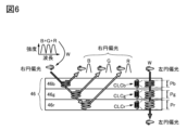
- FIG. 6 is a diagram illustrating an example of a reflective polarizer 46 having cholesteric liquid crystals.
- the reflective polarizer 46 is shown to have a three-layer structure of layers 46b, 46g, and 46r.
- Each of layers 46b, 46g, and 46r can be called a cholesteric liquid crystal layer.
- Layer 46b has cholesteric liquid crystal CLCb
- layer 46g has cholesteric liquid crystal CLCg
- layer 46r has cholesteric liquid crystal CLCr.
- the cholesteric liquid crystals CLCb, CLCg, and CLCr have a helical structure, and each has a different helical pitch.
- the product of the helical pitch Pb and the refractive index of the cholesteric liquid crystal CLCb in layer 46b corresponds to the wavelength of blue light.
- the product of the helical pitch Pg and the refractive index of the cholesteric liquid crystal CLCg in layer 46g corresponds to the wavelength of green light.
- the product of the helical pitch Pr and the refractive index of the cholesteric liquid crystal CLCr in layer 46r corresponds to the wavelength of red light. Since the refractive indices of the cholesteric liquid crystals CLCb, CLCg, and CLCr are approximately equal, it can be said that helical pitch Pb ⁇ helical pitch Pg ⁇ helical pitch Pr. Furthermore, each of the cholesteric liquid crystals CLCb, CLCg, and CLCr has a right-handed helical structure.
- white light W is composed of the three primary colors of light: blue light B, green light G, and red light R.
- the RGB lights actually emitted from the display panel 20 are not monochromatic, but each has a broad wavelength distribution.
- liquid crystal molecules that make up cholesteric liquid crystal have anisotropy in refractive index, and the product of the refractive index and the helical pitch takes values within a certain range. Cholesteric liquid crystal can reflect light with wavelengths equal to the values within this range.
- the refractive index and helical pitch of the cholesteric liquid crystal are appropriate, it can reflect the incident RGB color light even if it is broad.
- right-handed circularly polarized light with a wavelength in the range of blue light to red light e.g., 430 nm to 780 nm
- Figure 6 shows a simplified illustration of reflection at each layer, in cholesteric liquid crystals, Bragg reflection occurs, in which a reflective surface is formed for each helical pitch. Furthermore, if the cholesteric liquid crystals CLCb, CLCg, and CLCr each have a left-handed helical structure, the above explanation of reflection and transmission will be reversed, and the incident right-handed circularly polarized light will be transmitted, and the left-handed circularly polarized light will be reflected.
- FIG. 7A is a block diagram illustrating a display panel 20 included in an electronic device according to one embodiment of the present invention.
- the display panel 20 includes a pixel array 74, a circuit 75, and a circuit 76.
- the pixel array 74 includes pixels 70 arranged in columns and rows.
- a pixel 70 can have multiple sub-pixels 71.
- the sub-pixels 71 have the function of emitting light for display.
- a full-color display can be achieved by assigning colors such as R (red), G (green), and B (blue) to the light emitted by the sub-pixels 71.
- the subpixel 71 has a light-emitting device that emits visible light.
- an EL element such as an OLED (organic light-emitting diode) or a QLED (quantum-dot light-emitting diode).
- Examples of light-emitting materials that the EL element has include a material that emits fluorescence (fluorescent material), a material that emits phosphorescence (phosphorescent material), a material that exhibits thermally activated delayed fluorescence (thermally activated delayed fluorescence (TADF) material), and an inorganic compound (such as a quantum dot material).
- an LED such as a micro LED (light-emitting diode) can also be used as the light-emitting device.
- a non-light-emitting device such as a liquid crystal device can also be used for the subpixel 71.
- Circuit 75 and circuit 76 are driver circuits for driving subpixel 71.
- Circuit 75 can function as a source driver circuit, and circuit 76 can function as a gate driver circuit.
- Circuit 75 and circuit 76 can be, for example, a shift register circuit.
- the display panel may be divided vertically and horizontally into multiple regions, and pixels may be driven for each divided region.
- the circuits 75 and 76 can be separately arranged under the pixel array 74.
- the display panel 20 can have a laminated structure of layers 77 and 78, and multiple circuits 75 and multiple circuits 76 can be provided on the layer 77, with the pixel array 74 provided on the layer 78 so as to overlap them.
- the pixel array 74 can be driven for each divided area.
- the pixel array 74 can be operated at different frame rates in parts.
- the pixel array 74 can be displayed at different resolutions in parts, and can also be made compatible with foveated rendering.
- the wiring length can be shortened and the wiring capacitance can be reduced. This allows for a display panel that can operate at high speed and with low power consumption.
- the display panel 20 can have a narrow frame.
- circuits 75 and 76 shown in FIG. 7B are merely examples and can be changed as appropriate. Part of the circuits 75 and 76 can also be formed in the same layer as the pixel array 74. Layer 77 may also include circuits such as a memory circuit, an arithmetic circuit, and a communication circuit.
- this configuration can be achieved by providing layer 77 on a single crystal silicon substrate, forming circuits 75 and 76 with transistors having silicon in their channel formation regions (hereinafter, Si transistors), and forming pixel circuits of pixel array 74 provided in layer 78 with transistors having metal oxide in their channel formation regions (hereinafter, OS transistors).
- OS transistors can be formed using thin films and can be stacked on Si transistors.
- a structure may be used in which a layer 79 in which an OS transistor is provided is provided between the layer 77 and the layer 78.
- the layer 79 may be provided with an OS transistor that forms part of a pixel circuit included in the pixel array 74.
- the layer 79 may be provided with an OS transistor that forms part of the circuit 75 and the circuit 76.
- the layer 77 may be provided with an OS transistor that forms part of a circuit such as a memory circuit, an arithmetic circuit, or a communication circuit.
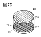
- the shape of the top surface of the display panel 20 is not limited to a rectangle, but may be a circle as shown in FIG. 7D. Or, it may be a polygon, such as an octagon, as shown in FIG. 7E.
- FIG. 8 is a diagram showing an example of a glasses-type device having the display panel 20 and optical device 60 shown in FIG. 1.
- the combination of the display panel 20 and the optical device 60 is shown by dashed lines as a display unit 92.
- the glasses-type device has two sets of display units 92.
- the housing 90 has a translucent section on the front side, through which external light is introduced into the display unit 92.
- the user can see the light of the display panel 20 of the display unit 92 superimposed on the external light.
- Virtual information can be displayed on the display panel 20.
- the user can see the scene and the display superimposed on each other, and can experience augmented reality in which virtual information is superimposed on reality.
- the housing 90 or the band 91 may be provided with an input terminal and an output terminal.
- the input terminal can be connected to a cable that supplies a video signal from a video output device or the like, or power for charging a battery provided within the housing 90.
- the output terminal can function as an audio output terminal, for example, and earphones, headphones, etc. can be connected. Note that if the configuration is such that audio data can be output via wireless communication, or if audio is output from an external video output device, the audio output terminal does not need to be provided.
- a wireless communication module and a storage module may be provided inside the housing 90 or the band 91.
- the wireless communication module performs wireless communication, and the content to be viewed can be downloaded and stored in the storage module. This allows the user to view the downloaded content offline. It is also possible to connect to the Internet and retrieve information about the scene being viewed.
- a line-of-sight detection sensor may be provided inside the housing 90.
- operation buttons such as power on, power off, sleep, volume adjustment, channel change, menu display, selection, decision, and back, as well as operation buttons for playing, stopping, pausing, fast forwarding, and rewinding videos may be displayed, and the respective operations can be performed by visually checking the operation buttons.
- optical device 60 By using the optical device 60 according to one embodiment of the present invention in a glasses-type device, it is possible to produce a small, thin, low-power-consumption, and highly reliable electronic device.
- This embodiment can be implemented in combination with at least a portion of the other embodiments and examples described in this specification.
- Embodiment 2 In this embodiment, a structure example of a display panel that can be applied to an electronic device of one embodiment of the present invention will be described.
- the display panel described below can be applied to the display panel 20 in Embodiment 1.
- One embodiment of the present invention is a display panel having light-emitting elements (also called light-emitting devices).
- the display panel has two or more pixels that emit light of different colors. Each pixel has a light-emitting element. Each light-emitting element has a pair of electrodes and an EL layer between them.
- the light-emitting element is preferably an organic EL element (organic electroluminescent element). Two or more light-emitting elements that emit different light colors each have an EL layer that contains a different light-emitting material.
- a full-color display panel can be realized by having three types of light-emitting elements that emit red (R), green (G), or blue (B) light.
- the shape and position of the island-shaped organic film deviate from the design, making it difficult to achieve high definition and high aperture ratio of the display panel.
- the contour of the layer may become blurred and the thickness of the edge may become thin. In other words, the thickness of the island-shaped light-emitting layer may vary depending on the location.
- an island-like light-emitting layer refers to a state in which the light-emitting layer is physically separated from the adjacent light-emitting layer.
- the EL layer is processed into a fine pattern by photolithography without using a shadow mask such as a fine metal mask (FMM).
- FMM fine metal mask
- the EL layer can be produced separately, a display panel that is extremely vivid, has high contrast, and has high display quality can be realized.
- the EL layer may be processed into a fine pattern by using both a metal mask and photolithography.
- a part or the whole of the EL layer can be physically separated. This makes it possible to suppress leakage current between light-emitting elements via a layer shared between adjacent light-emitting elements (also called a common layer). This makes it possible to prevent unintended light emission due to crosstalk, and to realize a display panel with extremely high contrast. In particular, a display panel with high current efficiency at low luminance can be realized.
- One embodiment of the present invention can be a display panel that combines a white light-emitting light-emitting element and a color filter.
- light-emitting elements of the same configuration can be applied to light-emitting elements provided in pixels (subpixels) that emit light of different colors, and all layers can be common layers.
- a part or all of each EL layer may be divided by a process using a photolithography method. This suppresses leakage current through the common layer, and a display panel with high contrast can be realized.
- an insulating layer that covers at least the side surface of the island-shaped light-emitting layer.
- the insulating layer may be configured to cover a part of the upper surface of the island-shaped EL layer.
- a material that has barrier properties against water and oxygen For example, an inorganic insulating film that does not easily diffuse water or oxygen can be used. This makes it possible to suppress deterioration of the EL layer and realize a highly reliable display panel.
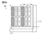
- FIG. 9A is a schematic top view of a display panel 100 according to one embodiment of the present invention.
- the display panel 100 includes a plurality of light-emitting elements 110R that exhibit red light, a plurality of light-emitting elements 110G that exhibit green light, and a plurality of light-emitting elements 110B that exhibit blue light, over a substrate 101.
- the symbols R, G, and B are assigned within the light-emitting regions of the light-emitting elements in order to easily distinguish between the light-emitting elements.
- Light emitting elements 110R, 110G, and 110B are each arranged in a matrix.
- Figure 9A shows a so-called stripe arrangement in which light emitting elements of the same color are arranged in one direction. Note that the arrangement method of the light emitting elements is not limited to this, and arrangement methods such as an S stripe arrangement, a delta arrangement, a Bayer arrangement, or a zigzag arrangement may also be applied, and a pentile arrangement, diamond arrangement, etc. may also be used.
- the light-emitting element 110R, the light-emitting element 110G, and the light-emitting element 110B it is preferable to use, for example, an OLED (organic light-emitting diode) or a QLED (quantum-dot light-emitting diode).
- OLED organic light-emitting diode
- QLED quantum-dot light-emitting diode
- the light-emitting material possessed by the EL element not only organic compounds but also inorganic compounds (such as quantum dot materials) can be used.
- FIG. 9A also shows a connection electrode 111C that is electrically connected to the common electrode 113.
- the connection electrode 111C is given a potential (e.g., an anode potential or a cathode potential) to be supplied to the common electrode 113.
- the connection electrode 111C is provided outside the display area where the light-emitting elements 110R and the like are arranged.
- the connection electrode 111C can be provided along the periphery of the display area. For example, it may be provided along one side of the periphery of the display area, or it may be provided over two or more sides of the periphery of the display area. In other words, if the top surface shape of the display area is rectangular, the top surface shape of the connection electrode 111C can be a strip shape (rectangle), an L-shape, a U-shape (square bracket shape), a square shape, or the like. Note that in this specification, the top surface shape refers to the shape in a plan view, that is, the shape when viewed from above.
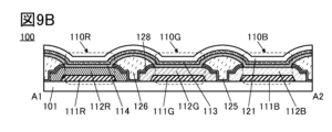
- Figures 9B and 9C are schematic cross-sectional views corresponding to dashed lines A1-A2 and A3-A4 in Figure 9A, respectively.
- Figure 9B shows schematic cross-sectional views of light-emitting element 110R, light-emitting element 110G, and light-emitting element 110B
- Figure 9C shows a schematic cross-sectional view of connection portion 140 where connection electrode 111C and common electrode 113 are connected.
- Light-emitting element 110R has pixel electrode 111R, organic layer 112R, common layer 114, and common electrode 113.
- Light-emitting element 110G has pixel electrode 111G, organic layer 112G, common layer 114, and common electrode 113.
- Light-emitting element 110B has pixel electrode 111B, organic layer 112B, common layer 114, and common electrode 113.
- Common layer 114 and common electrode 113 are provided in common to light-emitting element 110R, light-emitting element 110G, and light-emitting element 110B.
- the organic layer 112R of the light-emitting element 110R has a light-emitting organic compound that emits at least red light.
- the organic layer 112G of the light-emitting element 110G has a light-emitting organic compound that emits at least green light.
- the organic layer 112B of the light-emitting element 110B has a light-emitting organic compound that emits at least blue light.
- the organic layers 112R, 112G, and 112B can each be called an EL layer, and have at least a layer (light-emitting layer) that contains a light-emitting substance.
- light-emitting element 110R when describing matters common to light-emitting element 110R, light-emitting element 110G, and light-emitting element 110B, they may be referred to as light-emitting element 110.
- components distinguished by alphabets such as organic layer 112R, organic layer 112G, and organic layer 112B, they may be described using symbols without the alphabet.
- the organic layer 112 and the common layer 114 can each independently have one or more of an electron injection layer, an electron transport layer, a hole injection layer, and a hole transport layer.
- the organic layer 112 can have a laminated structure of a hole injection layer, a hole transport layer, a light-emitting layer, and an electron transport layer from the pixel electrode 111 side, and the common layer 114 can have an electron injection layer.
- the pixel electrode 111R, pixel electrode 111G, and pixel electrode 111B are provided for each light-emitting element.
- the common electrode 113 and common layer 114 are provided as a continuous layer common to each light-emitting element.
- a conductive film having transparency to visible light is used for either one of the pixel electrodes or the common electrode 113, and a conductive film having reflectivity is used for the other.
- a protective layer 121 is provided on the common electrode 113, covering the light-emitting elements 110R, 110G, and 110B.
- the protective layer 121 has the function of preventing impurities such as water from diffusing from above into each light-emitting element.
- the end of the pixel electrode 111 is preferably tapered.
- the organic layer 112 provided along the end of the pixel electrode 111 can also be tapered.
- the coverage of the organic layer 112 provided over the end of the pixel electrode 111 can be improved.
- foreign matter for example, also called dust or particles
- a tapered shape refers to a shape in which at least a portion of the side of the structure is inclined with respect to the substrate surface.
- the organic layer 112 is processed into an island shape using photolithography. Therefore, the angle between the top surface and the side surface of the organic layer 112 at its ends is close to 90 degrees.
- organic films formed using FMM (Fine Metal Mask) or the like tend to become gradually thinner closer to the ends.
- the top surface is formed in a slope shape over a range of 1 ⁇ m to 10 ⁇ m from the ends, making it difficult to distinguish between the top surface and the side surface.
- an insulating layer 125 Between two adjacent light-emitting elements are an insulating layer 125, a resin layer 126 and a layer 128.
- the resin layer 126 is located between the two adjacent light-emitting elements and is provided so as to fill the ends of each organic layer 112 and the area between the two organic layers 112.
- the resin layer 126 has a smooth convex upper surface shape, and a common layer 114 and a common electrode 113 are provided covering the upper surface of the resin layer 126.
- the resin layer 126 functions as a planarizing film that fills in the step between two adjacent light-emitting elements. By providing the resin layer 126, it is possible to prevent the phenomenon in which the common electrode 113 is divided by the step at the end of the organic layer 112 (also called step disconnection), which occurs and causes the common electrode on the organic layer 112 to become insulated.
- An insulating layer containing an organic material can be suitably used as the resin layer 126.
- acrylic resin, polyimide resin, epoxy resin, imide resin, polyamide resin, polyimideamide resin, silicone resin, siloxane resin, benzocyclobutene resin, phenol resin, and precursors of these resins can be used as the resin layer 126.
- organic materials such as polyvinyl alcohol (PVA), polyvinyl butyral, polyvinylpyrrolidone, polyethylene glycol, polyglycerin, pullulan, water-soluble cellulose, or alcohol-soluble polyamide resin can also be used as the resin layer 126.
- a photosensitive resin can be used as the resin layer 126.
- a photoresist can be used as the photosensitive resin.
- a positive type material or a negative type material can be used as the photosensitive resin.
- the resin layer 126 may contain a material that absorbs visible light.
- the resin layer 126 itself may be made of a material that absorbs visible light, or the resin layer 126 may contain a pigment that absorbs visible light.
- the resin layer 126 may be, for example, a resin that can be used as a color filter that transmits red, blue, or green light and absorbs other light, or a resin that contains carbon black as a pigment and functions as a black matrix.
- the insulating layer 125 is provided in contact with the side surface of the organic layer 112.
- the insulating layer 125 is also provided to cover the upper end portion of the organic layer 112.
- a portion of the insulating layer 125 is also provided in contact with the upper surface of the substrate 101.
- the insulating layer 125 is located between the resin layer 126 and the organic layer 112, and functions as a protective film to prevent the resin layer 126 from contacting the organic layer 112. If the organic layer 112 and the resin layer 126 come into contact with each other, the organic layer 112 may be dissolved by the organic solvent used in forming the resin layer 126. Therefore, by providing the insulating layer 125 between the organic layer 112 and the resin layer 126, it is possible to protect the side surface of the organic layer 112.
- the insulating layer 125 may be an insulating layer having an inorganic material.
- an inorganic insulating film such as an oxide insulating film, a nitride insulating film, an oxynitride insulating film, and a nitride oxide insulating film may be used for the insulating layer 125.
- the insulating layer 125 may have a single layer structure or a laminated structure.
- the oxide insulating film examples include a silicon oxide film, an aluminum oxide film, a magnesium oxide film, an indium gallium zinc oxide film, a gallium oxide film, a germanium oxide film, an yttrium oxide film, a zirconium oxide film, a lanthanum oxide film, a neodymium oxide film, a hafnium oxide film, and a tantalum oxide film.
- the nitride insulating film include a silicon nitride film and an aluminum nitride film.
- the oxynitride insulating film examples include a silicon oxynitride film and an aluminum oxynitride film.
- nitride oxide insulating film examples include a silicon nitride oxide film and an aluminum nitride oxide film.
- an inorganic insulating film such as an aluminum oxide film or a hafnium oxide film formed by the ALD method to the insulating layer 125, an insulating layer 125 with few pinholes and excellent function of protecting the EL layer can be formed.
- oxynitride refers to a material whose composition contains more oxygen than nitrogen
- nitride oxide refers to a material whose composition contains more nitrogen than oxygen
- silicon oxynitride refers to a material whose composition contains more oxygen than nitrogen
- silicon nitride oxide refers to a material whose composition contains more nitrogen than oxygen
- the insulating layer 125 can be formed by a sputtering method, a CVD method, a PLD method, an ALD method, or the like. It is preferable to form the insulating layer 125 by an ALD method, which has good coverage.
- a reflective film e.g., a metal film containing one or more selected from silver, palladium, copper, titanium, aluminum, etc.
- a reflective film may be provided between the insulating layer 125 and the resin layer 126, and the light emitted from the light-emitting layer may be reflected by the reflective film. This can improve the light extraction efficiency.
- Layer 128 is a portion of a protective layer (also called a mask layer or a sacrificial layer) for protecting organic layer 112 when the organic layer 112 is etched.
- the material that can be used for insulating layer 125 can be used for layer 128. In particular, it is preferable to use the same material for layer 128 and insulating layer 125 because the same processing equipment can be used.
- inorganic insulating films such as aluminum oxide films, metal oxide films such as hafnium oxide films, and silicon oxide films formed by the ALD method have few pinholes, so they have excellent protection properties for the EL layer and can be suitably used for the insulating layer 125 and layer 128.
- the protective layer 121 can have, for example, a single-layer structure or a laminated structure including at least an inorganic insulating film.
- the inorganic insulating film include oxide films or nitride films such as a silicon oxide film, a silicon oxynitride film, a silicon nitride oxide film, a silicon nitride film, an aluminum oxide film, an aluminum oxynitride film, and a hafnium oxide film.
- a semiconductor material or a conductive material such as indium gallium oxide, indium zinc oxide, indium tin oxide, or indium gallium zinc oxide may be used as the protective layer 121.
- the protective layer 121 may be a laminated film of an inorganic insulating film and an organic insulating film.
- an organic insulating film is sandwiched between a pair of inorganic insulating films.
- the organic insulating film functions as a planarizing film. This allows the upper surface of the organic insulating film to be flat, improving the coverage of the inorganic insulating film thereon and enhancing the barrier properties.
- the upper surface of the protective layer 121 is flat, it is preferable that when a structure (e.g., a color filter, an electrode of a touch sensor, or a lens array) is provided above the protective layer 121, the influence of the uneven shape caused by the structure below can be reduced.
- a structure e.g., a color filter, an electrode of a touch sensor, or a lens array
- FIG. 9C shows a connection portion 140 where the connection electrode 111C and the common electrode 113 are electrically connected.
- connection portion 140 an opening is provided in the insulating layer 125 and the resin layer 126 above the connection electrode 111C.
- the connection electrode 111C and the common electrode 113 are electrically connected in the opening.
- FIG. 9C shows a connection portion 140 that electrically connects the connection electrode 111C and the common electrode 113
- the common electrode 113 may be provided on the connection electrode 111C via the common layer 114.
- the electrical resistivity of the material used for the common layer 114 is sufficiently low and the common layer 114 can be formed thin, so there are many cases where no problem occurs even if the common layer 114 is located at the connection portion 140. This allows the common electrode 113 and the common layer 114 to be formed using the same shielding mask, thereby reducing manufacturing costs.
- FIG 10A shows a schematic cross-sectional view of display panel 100a.
- Display panel 100a differs from display panel 100 mainly in that the light-emitting element configuration is different and that display panel 100a has a colored layer.
- the display panel 100a has a light-emitting element 110W that emits white light.
- the light-emitting element 110W has a pixel electrode 111, an organic layer 112W, a common layer 114, and a common electrode 113.
- the organic layer 112W emits white light.
- the organic layer 112W can be configured to include two light-emitting materials whose emitted light colors are complementary to each other.
- the organic layer 112W can be configured to include a light-emitting organic compound that emits blue light and a light-emitting organic compound that emits yellow light.
- the organic layer 112W can also be configured to include a light-emitting organic compound that emits red light, a light-emitting organic compound that emits green light, and a light-emitting organic compound that emits blue light.
- the organic layers 112W are separated between two adjacent light-emitting elements 110W. This makes it possible to suppress leakage current flowing between adjacent light-emitting elements 110W via the organic layers 112W, and to suppress crosstalk caused by the leakage current. This makes it possible to realize a display panel with high contrast and color reproducibility.
- An insulating layer 122 that functions as a planarizing film is provided on the protective layer 121, and colored layers 116R, 116G, and 116B are provided on the insulating layer 122.
- the insulating layer 122 can be an organic resin film or an inorganic insulating film with a flattened upper surface.
- the insulating layer 122 forms the surface on which the colored layers 116R, 116G, and 116B are formed. Therefore, by making the upper surface of the insulating layer 122 flat, the thickness of the colored layers 116R, etc. can be made uniform, thereby improving the color purity. Note that if the thickness of the colored layers 116R, etc. is not uniform, the amount of light absorbed varies depending on the location of the colored layer 116R, which may result in a decrease in color purity.
- FIG. 10B shows a schematic cross-sectional view of the display panel 100b.
- Light-emitting element 110R has pixel electrode 111, conductive layer 115R, organic layer 112W, and common electrode 113.
- Light-emitting element 110G has pixel electrode 111, conductive layer 115G, organic layer 112W, and common electrode 113.
- Light-emitting element 110B has pixel electrode 111, conductive layer 115B, organic layer 112W, and common electrode 113.
- Conductive layer 115R, conductive layer 115G, and conductive layer 115B each have translucency and function as an optical adjustment layer.
- a microresonator (microcavity) structure By using a film that reflects visible light for the pixel electrode 111 and a film that is both reflective and transparent to visible light for the common electrode 113, a microresonator (microcavity) structure can be realized.
- a microresonator (microcavity) structure By adjusting the thicknesses of the conductive layers 115R, 115G, and 115B so as to provide optimal optical path lengths, even when an organic layer 112 that emits white light is used, light with different wavelengths that are intensified can be obtained from the light-emitting elements 110R, 110G, and 110B.
- colored layers 116R, 116G, and 116B are provided on the optical paths of light-emitting elements 110R, 110G, and 110B, respectively, to obtain light with high color purity.
- Insulating layer 123 is provided to cover the ends of pixel electrode 111, conductive layer 115R, conductive layer 115G, and conductive layer 115B. It is preferable that insulating layer 123 has a tapered end. Providing insulating layer 123 can improve coverage by organic layer 112W, common electrode 113, protective layer 121, and the like formed thereon.
- the organic layer 112W and the common electrode 113 are each provided as a continuous film common to each light-emitting element. This configuration is preferable because it greatly simplifies the manufacturing process of the display panel.
- the pixel electrode 111 has an end shape that is nearly vertical. This allows a steeply inclined portion to be formed on the surface of the insulating layer 123, and a thin portion can be formed in the part of the organic layer 112W that covers this portion, or a part of the organic layer 112W can be separated. Therefore, it is possible to suppress leakage current through the organic layer 112W that occurs between adjacent light-emitting elements without processing the organic layer 112W using a photolithography method or the like.
- the top surface shape of the subpixel may be, for example, a triangle, a quadrangle (including a rectangle and a square), a polygon such as a pentagon, a polygon with rounded corners, an ellipse, or a circle.
- the top surface shape of the subpixel corresponds to the top surface shape of the light-emitting region of the light-emitting element.
- the pixel 150 shown in FIG. 11A has an S-stripe arrangement.
- the pixel 150 shown in FIG. 11A is composed of three sub-pixels, light-emitting elements 110a, 110b, and 110c.
- the light-emitting element 110a may be a blue light-emitting element
- the light-emitting element 110b may be a red light-emitting element
- the light-emitting element 110c may be a green light-emitting element.
- the pixel 150 shown in FIG. 11B has a light-emitting element 110a having a top surface shape of a roughly trapezoid or triangle with rounded corners, a light-emitting element 110b having a top surface shape of a roughly trapezoid or triangle with rounded corners, and a light-emitting element 110c having a top surface shape of a roughly rectangular or hexagon with rounded corners. Furthermore, the light-emitting element 110a has a larger light-emitting area than the light-emitting element 110b. In this way, the shape and size of each light-emitting element can be determined independently. For example, the more reliable the light-emitting element, the smaller the size can be.
- the light-emitting element 110a may be a green light-emitting element
- the light-emitting element 110b may be a red light-emitting element
- the light-emitting element 110c may be a blue light-emitting element.
- the pixels 124a and 124b shown in FIG. 11C are arranged in a Pentile array.
- FIG. 11C shows an example in which pixel 124a having light-emitting elements 110a and 110b and pixel 124b having light-emitting elements 110b and 110c are arranged alternately.
- light-emitting element 110a may be a red light-emitting element
- light-emitting element 110b may be a green light-emitting element
- light-emitting element 110c may be a blue light-emitting element.
- Pixels 124a and 124b shown in Figures 11D and 11E are arranged in a delta arrangement.
- Pixel 124a has two light-emitting elements (light-emitting elements 110a and 110b) in the top row (first row) and one light-emitting element (light-emitting element 110c) in the bottom row (second row).
- Pixel 124b has one light-emitting element (light-emitting element 110c) in the top row (first row) and two light-emitting elements (light-emitting elements 110a and 110b) in the bottom row (second row).
- light-emitting element 110a may be a red light-emitting element
- light-emitting element 110b may be a green light-emitting element
- light-emitting element 110c may be a blue light-emitting element.
- Figure 11D shows an example in which each light-emitting element has a generally rectangular top surface shape with rounded corners
- Figure 11E shows an example in which each light-emitting element has a circular top surface shape.
- Figure 11F shows an example in which light-emitting elements of each color are arranged in a zigzag pattern.
- the positions of the upper edges of two light-emitting elements e.g., light-emitting elements 110a and 110b, or light-emitting elements 110b and 110c
- light-emitting element 110a may be a red light-emitting element
- light-emitting element 110b may be a green light-emitting element
- light-emitting element 110c may be a blue light-emitting element.
- the finer the pattern to be processed the more the effects of light diffraction cannot be ignored, and this causes a loss of fidelity when the photomask pattern is transferred by exposure, making it difficult to process the resist mask into the desired shape.
- the photomask pattern is rectangular, a pattern with rounded corners is likely to be formed.
- the top surface shape of the light-emitting element may become a polygon with rounded corners, an ellipse, a circle, or the like.
- the EL layer is processed into an island shape using a resist mask.
- the resist film formed on the EL layer needs to be cured at a temperature lower than the heat resistance temperature of the EL layer. Therefore, depending on the heat resistance temperature of the material of the EL layer and the curing temperature of the resist material, the resist film may not be cured sufficiently.
- a resist film that is not cured sufficiently may have a shape different from the desired shape during processing.
- the top surface shape of the EL layer may become a polygon with rounded corners, an ellipse, a circle, or the like. For example, when attempting to form a resist mask with a square top surface shape, a resist mask with a circular top surface shape is formed, and the top surface shape of the EL layer may become circular.
- OPC Optical Proximity Correction
- This embodiment can be implemented in combination with at least a portion of the other embodiments described in this specification.
- the display panel of this embodiment is a high-definition display panel, and is particularly suitable for use as the display unit of VR devices such as head-mounted displays, and wearable devices that can be worn on the head, such as glasses-type AR devices.
- the display module 280 has a substrate 291 and a substrate 292.
- the display module 280 has a display unit 281.
- the display unit 281 is an area that displays an image.
- Figure 12B shows a perspective view that shows a schematic configuration on the substrate 291 side.
- a circuit section 282 On the substrate 291, a circuit section 282, a pixel circuit section 283 on the circuit section 282, and a pixel section 284 on the pixel circuit section 283 are stacked.
- a terminal section 285 for connecting to an FPC 290 is provided in a portion of the substrate 291 that does not overlap with the pixel section 284.
- the terminal section 285 and the circuit section 282 are electrically connected by a wiring section 286 that is composed of multiple wirings.
- the pixel circuit section 283 has a number of pixel circuits 283a arranged periodically. Each pixel circuit 283a is a circuit that controls the light emission of three light-emitting devices in one pixel 284a.
- One pixel circuit 283a may be configured to have three circuits that control the light emission of one light-emitting device.
- the pixel circuit 283a may be configured to have at least one selection transistor, one current control transistor (drive transistor), and a capacitance element for each light-emitting device. At this time, a gate signal is input to the gate of the selection transistor, and a source signal is input to the source. This realizes an active matrix display panel.
- the circuit portion 282 has a circuit that drives each pixel circuit 283a of the pixel circuit portion 283.
- a gate line driver circuit and a source line driver circuit may have at least one of an arithmetic circuit, a memory circuit, a power supply circuit, etc.
- a transistor provided in the circuit portion 282 may constitute a part of the pixel circuit 283a. That is, the pixel circuit 283a may be composed of a transistor included in the pixel circuit portion 283 and a transistor included in the circuit portion 282.
- the FPC 290 functions as wiring for supplying video signals, power supply potential, etc. from the outside to the circuit section 282.
- An IC may also be mounted on the FPC 290.
- the display module 280 can be configured such that one or both of the pixel circuit section 283 and the circuit section 282 are provided overlappingly under the pixel section 284, so that the aperture ratio (effective display area ratio) of the display section 281 can be extremely high.
- the aperture ratio of the display section 281 can be 40% or more and less than 100%, preferably 50% or more and 95% or less, and more preferably 60% or more and 95% or less.
- the pixels 284a can be arranged at an extremely high density, so that the pixel density of the display section 281 can be extremely high.
- the pixels 284a are arranged in the display section 281 at a pixel density of 2000 ppi or more, preferably 3000 ppi or more, more preferably 5000 ppi or more, and even more preferably 6000 ppi or more, and 20000 ppi or less, or 30000 ppi or less.
- Such a display module 280 has extremely high resolution and can therefore be suitably used in VR devices such as head-mounted displays, or in glasses-type AR devices.
- the display module 280 has an extremely high resolution display section 281, so that even if the display section is enlarged with a lens, the pixels are not visible, and a highly immersive display can be achieved.
- the display module 280 is not limited to this, and can be suitably used in electronic devices with relatively small display sections. For example, it can be suitably used in the display section of a wearable electronic device such as a wristwatch.
- the display panel 200A shown in FIG. 13 includes a substrate 301, light emitting elements 110R, 110G, and 110B, a capacitor 240, and a transistor 310.
- an element isolation layer 315 is provided between two adjacent transistors 310 so as to be embedded in the substrate 301.
- an insulating layer 261 is provided covering the transistor 310, and a capacitor 240 is provided on the insulating layer 261.
- the conductive layer 241 is provided on the insulating layer 261 and is embedded in the insulating layer 254.
- the conductive layer 241 is electrically connected to one of the source and drain of the transistor 310 by a plug 271 embedded in the insulating layer 261.
- the insulating layer 243 is provided to cover the conductive layer 241.
- the conductive layer 245 is provided in a region that overlaps with the conductive layer 241 via the insulating layer 243.
- An insulating layer 255a is provided covering the capacitor 240, an insulating layer 255b is provided on the insulating layer 255a, and an insulating layer 255c is provided on the insulating layer 255b.
- Insulating layer 255a, insulating layer 255b, and insulating layer 255c can each suitably be made of an inorganic insulating film.
- a silicon oxide film for insulating layer 255a and insulating layer 255c and a silicon nitride film for insulating layer 255b. This allows insulating layer 255b to function as an etching protection film.
- an example is shown in which part of insulating layer 255c is etched to form a recess, but insulating layer 255c does not necessarily have to have a recess.
- Light-emitting elements 110R, 110G, and 110B are provided on insulating layer 255c.
- the configurations of light-emitting elements 110R, 110G, and 110B can be seen in embodiment 2.
- the display panel 200A a different light-emitting device is created for each emitted color, so there is little change in chromaticity between light emitted at low and high luminance.
- the organic layers 112R, 112G, and 112B are spaced apart from each other, the occurrence of crosstalk between adjacent subpixels can be suppressed even in a high-definition display panel. This makes it possible to realize a display panel that is both high-definition and has high display quality.
- Insulating layer 125, resin layer 126, and layer 128 are provided in the area between adjacent light-emitting elements.
- the pixel electrodes 111R, 111G, and 111B of the light-emitting element are electrically connected to one of the source and drain of the transistor 310 by a plug 256 embedded in the insulating layers 255a, 255b, and 255c, a conductive layer 241 embedded in the insulating layer 254, and a plug 271 embedded in the insulating layer 261.
- the height of the top surface of the insulating layer 255c and the height of the top surface of the plug 256 are the same or approximately the same.
- Various conductive materials can be used for the plug.
- Display panel 200B] 14 has a configuration in which a transistor 310A, each of which has a channel formed in a semiconductor substrate, and a transistor 310B are stacked together. Note that in the following description of the display panel, description of parts that are the same as those of the display panel described above may be omitted.
- the display panel 200B has a structure in which a substrate 301B on which a transistor 310B, a capacitor 240, and a light-emitting device are provided, and a substrate 301A on which a transistor 310A is provided are bonded together.
- an insulating layer 345 is provided on the lower surface of the substrate 301B, and an insulating layer 346 is provided on the insulating layer 261 provided on the substrate 301A.
- the insulating layers 345 and 346 function as protective layers, and can suppress the diffusion of impurities into the substrates 301B and 301A.
- the insulating layers 345 and 346 can be made of an inorganic insulating film that can be used for the protective layer 121.
- Substrate 301B is provided with plug 343 penetrating substrate 301B and insulating layer 345.
- insulating layer 344 that covers the side surface of plug 343 and functions as a protective layer.
- the substrate 301B has a conductive layer 342 provided below the insulating layer 345.
- the conductive layer 342 is embedded in the insulating layer 335, and the lower surfaces of the conductive layer 342 and the insulating layer 335 are flattened.
- the conductive layer 342 is also electrically connected to the plug 343.
- the substrate 301A has a conductive layer 341 provided on an insulating layer 346.
- the conductive layer 341 is embedded in the insulating layer 336, and the upper surfaces of the conductive layer 341 and the insulating layer 336 are flattened.
- the conductive layers 341 and 342 are preferably made of the same conductive material.
- a metal film containing an element selected from Al, Cr, Cu, Ta, Ti, Mo, and W, or a metal nitride film containing the above-mentioned elements can be used.
- copper is preferably used for the conductive layers 341 and 342. This allows the application of Cu-Cu (copper-copper) direct bonding technology (a technology that achieves electrical conductivity by connecting Cu (copper) pads together).
- Display panel 200C The display panel 200C shown in FIG. 15 has a configuration in which a conductive layer 341 and a conductive layer 342 are bonded to each other via a bump 347.
- the conductive layer 341 and the conductive layer 342 can be electrically connected.
- the bump 347 can be formed using a conductive material including, for example, gold (Au), nickel (Ni), indium (In), tin (Sn), etc. In addition, for example, solder may be used as the bump 347.
- An adhesive layer 348 may be provided between the insulating layer 345 and the insulating layer 346. In addition, when the bump 347 is provided, the insulating layer 335 and the insulating layer 336 may not be provided.
- Display panel 200D The display panel 200D shown in FIG. 16 differs from the display panel 200A mainly in the configuration of the transistors.
- Transistor 320 is a transistor (OS transistor) in which a metal oxide (also called an oxide semiconductor) is applied to a semiconductor layer in which a channel is formed.
- OS transistor a transistor
- metal oxide also called an oxide semiconductor
- Transistor 320 has a semiconductor layer 321, an insulating layer 323, a conductive layer 324, a pair of conductive layers 325, an insulating layer 326, and a conductive layer 327.
- Substrate 331 corresponds to substrate 291 in Figures 12A and 12B.
- An insulating layer 332 is provided on the substrate 331.
- the insulating layer 332 functions as a barrier layer that prevents impurities such as water or hydrogen from diffusing from the substrate 331 to the transistor 320 and prevents oxygen from being released from the semiconductor layer 321 to the insulating layer 332 side.
- a film in which hydrogen or oxygen is less likely to diffuse than a silicon oxide film such as an aluminum oxide film, a hafnium oxide film, or a silicon nitride film, can be used.
- the semiconductor layer 321 is provided on the insulating layer 326.
- the semiconductor layer 321 preferably has a metal oxide (also called an oxide semiconductor) film that exhibits semiconductor characteristics.
- a pair of conductive layers 325 is provided on and in contact with the semiconductor layer 321 and functions as a source electrode and a drain electrode.
- An insulating layer 328 is provided to cover the top and side surfaces of the pair of conductive layers 325 and the side surfaces of the semiconductor layer 321, and an insulating layer 264 is provided on the insulating layer 328.
- the insulating layer 328 functions as a barrier layer that prevents impurities such as water or hydrogen from diffusing from the insulating layer 264 to the semiconductor layer 321 and prevents oxygen from being released from the semiconductor layer 321.
- the insulating layer 328 can be an insulating film similar to the insulating layer 332.
- An opening is provided in the insulating layer 328 and the insulating layer 264, reaching the semiconductor layer 321.
- the conductive layer 324 functions as a second gate electrode, and the insulating layer 323 functions as a second gate insulating layer.
- the upper surface of conductive layer 324, the upper surface of insulating layer 323, and the upper surface of insulating layer 264 are flattened so that their heights are the same or roughly the same, and insulating layers 329 and 265 are provided covering them.
- the insulating layer 264 and the insulating layer 265 function as interlayer insulating layers.
- the insulating layer 329 functions as a barrier layer that prevents impurities such as water or hydrogen from diffusing from the insulating layer 265 to the transistor 320.
- the insulating layer 329 can be an insulating film similar to the insulating layer 328 and the insulating layer 332 described above.
- the plug 274 electrically connected to one of the pair of conductive layers 325 is provided so as to be embedded in the insulating layer 265, the insulating layer 329, and the insulating layer 264.
- the plug 274 preferably has a conductive layer 274a covering the side surfaces of the openings of the insulating layer 265, the insulating layer 329, the insulating layer 264, and the insulating layer 328, and a part of the upper surface of the conductive layer 325, and a conductive layer 274b in contact with the upper surface of the conductive layer 274a.
- the structure of the transistor included in the display panel of this embodiment is not particularly limited.
- a planar type transistor, a staggered type transistor, an inverted staggered type transistor, or the like can be used.
- either a top-gate type or a bottom-gate type transistor structure may be used.
- a gate may be provided above and below a semiconductor layer in which a channel is formed.
- Transistor 320 has a configuration in which a semiconductor layer in which a channel is formed is sandwiched between two gates.
- the two gates may be connected and the transistor may be driven by supplying the same signal to them.
- the threshold voltage of the transistor may be controlled by applying a potential to one of the two gates for controlling the threshold voltage and a potential to drive the other.
- the crystallinity of the semiconductor material used in the semiconductor layer of the transistor is not particularly limited, and any of an amorphous semiconductor, a single crystal semiconductor, or a semiconductor having crystallinity other than single crystal (a microcrystalline semiconductor, a polycrystalline semiconductor, or a semiconductor having a crystalline region in part) may be used.
- the use of a single crystal semiconductor or a semiconductor having crystallinity is preferable because it can suppress deterioration of the transistor characteristics.
- the band gap of the metal oxide used in the semiconductor layer of the transistor is preferably 2 eV or more, and more preferably 2.5 eV or more.
- the metal oxide preferably contains at least indium or zinc, and more preferably contains indium and zinc.
- the metal oxide preferably contains indium, M (wherein M is one or more selected from gallium, aluminum, yttrium, tin, silicon, boron, copper, vanadium, beryllium, titanium, iron, nickel, germanium, zirconium, molybdenum, lanthanum, cerium, neodymium, hafnium, tantalum, tungsten, magnesium, and cobalt), and zinc.
- the semiconductor layer of the transistor may contain silicon.
- silicon examples include amorphous silicon and crystalline silicon (such as low-temperature polysilicon and single crystal silicon).
- metal oxides that can be used in the semiconductor layer include indium oxide, gallium oxide, and zinc oxide.
- the metal oxide preferably contains two or three elements selected from indium, element M, and zinc.
- the element M is one or more elements selected from gallium, aluminum, silicon, boron, yttrium, tin, copper, vanadium, beryllium, titanium, iron, nickel, germanium, zirconium, molybdenum, lanthanum, cerium, neodymium, hafnium, tantalum, tungsten, and magnesium.
- the element M is preferably one or more elements selected from aluminum, gallium, yttrium, and tin.
- the metal oxide is preferably formed by a sputtering method or an ALD method.
- the productivity can be increased and the film density can be increased.
- the metal oxide is formed by an ALD method, the coverage of the film can be increased.
- an oxide containing indium, gallium, and zinc also referred to as IGZO
- an oxide containing indium, tin, and zinc also referred to as ITZO (registered trademark)
- ITZO oxide containing indium, gallium, tin, and zinc
- IAZO oxide containing indium, aluminum, and zinc
- IAGZO oxide containing indium, aluminum, gallium, and zinc
- the metal oxide used in the semiconductor layer is an In-M-Zn oxide
- the atomic ratio of In in the In-M-Zn oxide is equal to or greater than the atomic ratio of M.
- element M gallium or tin
- element M may be a combination of two or more of the above elements.
- In:M:Zn 40:1:10 or metal oxides in the vicinity thereof for the semiconductor layer.
- the semiconductor layer may have two or more metal oxide layers with different compositions.
- a laminated structure of any one selected from indium oxide, indium gallium oxide, and IGZO and any one selected from IAZO, IAGZO, and ITZO (registered trademark) may be used.
- an oxide semiconductor having crystallinity for example, an oxide semiconductor having a CAAC (c-axis aligned crystal) structure, a polycrystalline (poly-crystal) structure, a nanocrystalline (nc: nano-crystal) structure, or the like can be used.
- the oxide semiconductor having crystallinity has a low defect level density, and can realize a highly reliable transistor.
- the CAAC structure is a crystal structure in which multiple microcrystals (typically multiple IGZO microcrystals) have a c-axis orientation, and the multiple microcrystals are connected without being oriented in the a-b plane.
- the CAAC structure has fewer crystal grain boundaries and grains in the a-b plane than the polycrystalline structure, and can realize a highly reliable transistor.
- OS transistors have extremely high field-effect mobility compared to transistors using amorphous silicon.
- the leakage current between the source and drain of an OS transistor in an off state (also referred to as off-state current) is extremely small, and the charge accumulated in a capacitor connected in series with the transistor can be held for a long period of time.
- the use of an OS transistor can reduce the power consumption of a display panel.
- the change in source-drain current in an OS transistor is smaller in response to a change in gate-source voltage than in a Si transistor. Therefore, by using an OS transistor as a driving transistor included in a pixel circuit, the current flowing between the source and drain can be precisely determined by changing the gate-source voltage, and the amount of current flowing to the light-emitting device can be controlled. This makes it possible to increase the number of gray levels in the pixel circuit.
- an OS transistor can pass a more stable current (saturation current) than a Si transistor, even when the source-drain voltage gradually increases. Therefore, by using an OS transistor as a driving transistor, a stable current can be passed to a light-emitting device, for example, even when the current-voltage characteristics of an EL device vary. In other words, when an OS transistor operates in the saturation region, the source-drain current hardly changes even when the source-drain voltage is increased, so the light emission luminance of the light-emitting device can be stabilized.
- a display panel 200F illustrated in FIG. 17 has a stacked structure of a transistor 310 in which a channel is formed in a substrate 301 and a transistor 320 in which a channel is formed and which contains metal oxide in a semiconductor layer.
- An insulating layer 261 is provided to cover the transistor 310, and a conductive layer 251 is provided on the insulating layer 261.
- An insulating layer 262 is provided to cover the conductive layer 251, and a conductive layer 252 is provided on the insulating layer 262.
- the conductive layers 251 and 252 each function as wiring.
- An insulating layer 263 and an insulating layer 332 are provided to cover the conductive layer 252, and a transistor 320 is provided on the insulating layer 332.
- An insulating layer 265 is provided to cover the transistor 320, and a capacitor 240 is provided on the insulating layer 265. The capacitor 240 and the transistor 320 are electrically connected by a plug 274.
- Transistor 320 can be used as a transistor that constitutes a pixel circuit.
- Transistor 310 can be used as a transistor that constitutes a pixel circuit, or a transistor that constitutes a driver circuit (gate line driver circuit, source line driver circuit) for driving the pixel circuit.
- Transistor 310 and transistor 320 can be used as transistors that constitute various circuits such as an arithmetic circuit or a memory circuit.
- This configuration allows not only pixel circuits but also drive circuits to be formed directly under the light-emitting device, making it possible to reduce the size of the display panel compared to when drive circuits are provided around the periphery of the display area.
- Display panel 200G The display panel 200G shown in Fig. 18 has a configuration in which the transistor 320 of the display panel 200F shown in Fig. 17 is replaced with a transistor 320A (vertical transistor). Note that the configuration in which the transistor 320 is replaced with the transistor 320A can also be applied to the display panel 200D shown in Fig. 16.
- Figure 19A shows a cross-sectional view of transistor 320A in the XZ plane.
- Figure 19B shows a cross-sectional view of transistor 320A in the XY plane, including wiring 440.
- Transistor 320A has an oxide semiconductor 470, an insulator 430, and a conductor 420.
- the oxide semiconductor 470 functions as a semiconductor layer
- the insulator 430 functions as a gate insulator
- the conductor 420 functions as a gate electrode.
- the wiring 450 has a region that functions as one of the source electrode and the drain electrode of transistor 320A.
- the wiring 440 has a region that functions as the other of the source electrode and the drain electrode of transistor 320A.
- An opening 490 is provided through the wiring 440 and the insulator 480, reaching the wiring 450.
- the opening 490 has a columnar shape with a roughly circular upper surface. This configuration allows for miniaturization or high integration of memory cells. Note that the side surface of the opening 490 is preferably perpendicular to the upper surface of the wiring 450.
- the insulator 430 is arranged so that at least a portion of it covers the opening 490.
- the conductor 420 is arranged so that at least a portion of it is located in the opening 490. It is preferable that the conductor 420 is provided so as to fill the opening 490, and the top surface shape is preferably roughly circular to increase the degree of integration.
- the oxide semiconductor 470 has a region 470i and regions 470na and 470nb arranged to sandwich the region 470i.
- Region 470na is a region of oxide semiconductor 470 that is in contact with wiring 450. At least a portion of region 470na functions as one of the source region and drain region of transistor 320A.
- Region 470nb is a region of oxide semiconductor 470 that is in contact with wiring 440. At least a portion of region 470nb functions as the other of the source region and drain region of transistor 320A.
- wiring 440 is in contact with the entire outer periphery of oxide semiconductor 470.
- the other of the source region and drain region of transistor 320A can be formed on the entire outer periphery of a portion of oxide semiconductor 470 that is formed in the same layer as wiring 440.
- the channel length of the transistor 320A is the distance between the source region and the drain region. In other words, it can be said that the channel length of the transistor 320A is determined by the thickness of the insulator 480 on the wiring 450.
- the channel length L of the transistor 320A is indicated by a dashed double-headed arrow.
- the channel length L is the distance between the end of the region where the oxide semiconductor 470 and the wiring 450 contact each other and the end of the region where the oxide semiconductor 470 and the wiring 440 contact each other in a cross-sectional view.
- the channel length L corresponds to the length of the side surface of the insulator 480 on the opening 490 side in a cross-sectional view.
- the channel length is set by the exposure limit of photolithography, but in one embodiment of the present invention, the channel length can be set by the film thickness of the insulator 480. Therefore, the channel length of the transistor 320A can be made to be an extremely fine structure that is below the exposure limit of photolithography (e.g., 60 nm or less, 50 nm or less, 40 nm or less, 30 nm or less, 20 nm or less, or 10 nm or less, and 1 nm or more, or 5 nm or more). This allows the on-current of the transistor 320A to be increased.
- the exposure limit of photolithography e.g. 60 nm or less, 50 nm or less, 40 nm or less, 30 nm or less, 20 nm or less, or 10 nm or less, and 1 nm or more, or 5 nm or more. This allows the on-current of the transistor 320A to be increased.
- the channel formation region, the source region, and the drain region can be formed in the opening 490. This allows the area occupied by the transistor 320A to be reduced compared to conventional transistors in which the channel formation region, the source region, and the drain region are provided separately on the XY plane. This allows the pixel density to be increased.
- a transistor having a channel formation region along the side of the insulator 480 in the opening 490 is also called a vertical transistor.
- the oxide semiconductor 470, the insulator 430, and the conductor 420 are arranged concentrically in the XY plane including the channel formation region of the oxide semiconductor 470. Therefore, the side surface of the conductor 420 arranged at the center faces the side surface of the oxide semiconductor 470 through the insulator 430. That is, in the top view, the entire circumference of the oxide semiconductor 470 becomes the channel formation region.
- the channel width of the transistor 320A is determined by the length of the outer periphery of the oxide semiconductor 470. That is, it can be said that the channel width of the transistor 320A is determined by the size of the maximum width of the opening 490 (maximum diameter when the opening 490 is circular in the top view).
- the maximum width D of the opening 490 is indicated by a double-headed arrow of a two-dot chain line.
- the channel width W of the transistor 320A is indicated by a double-headed arrow of a one-dot chain line.
- the maximum width D of the opening 490 is set by the exposure limit of photolithography.
- the maximum width D of the opening 490 is set by the film thickness of each of the oxide semiconductor 470, the insulator 430, and the conductor 420 provided in the opening 490.
- the maximum width D of the opening 490 is, for example, 5 nm or more, 10 nm or more, or 20 nm or more, and is preferably 100 nm or less, 60 nm or less, 50 nm or less, 40 nm or less, or 30 nm or less. Note that when the opening 490 is circular in top view, the maximum width D of the opening 490 corresponds to the diameter of the opening 490, and the channel width W can be calculated as "D x ⁇ ".
- the channel length L of the transistor 320A is preferably at least smaller than the channel width W of the transistor 320A.
- the channel length L of the transistor 320A according to one embodiment of the present invention is 0.1 to 0.99 times, preferably 0.5 to 0.8 times, the channel width W of the transistor 320A. With such a configuration, a transistor having good electrical characteristics and high reliability can be realized.
- a channel formation region of a transistor using an oxide semiconductor for a semiconductor layer preferably has fewer oxygen vacancies or a lower concentration of impurities such as hydrogen, nitrogen, or a metal element than the source and drain regions.
- the aluminum concentration in the channel formation region of the oxide semiconductor is preferably 1 ⁇ 10 22 atoms/cm 3 or less, more preferably 1 ⁇ 10 21 atoms/cm 3 or less, still more preferably 1 ⁇ 10 20 atoms/cm 3 or less, still more preferably 5 ⁇ 10 19 atoms/cm 3 or less, still more preferably 1 ⁇ 10 19 atoms/cm 3 or less, still more preferably 5 ⁇ 10 18 atoms/cm 3 or less, and still more preferably 1 ⁇ 10 18 atoms/cm 3 or less.
- the channel formation region of the transistor is a high-resistance region with a low carrier concentration. Therefore, the channel formation region of the transistor can be said to be i-type (intrinsic) or substantially i-type.
- the source and drain regions of a transistor that uses an oxide semiconductor for its semiconductor layer have more oxygen vacancies, more VOH , or a higher concentration of impurities such as hydrogen, nitrogen, or metal elements than the channel formation region, and thus have an increased carrier concentration and low resistance.
- the source and drain regions of the transistor are n-type regions that have a higher carrier concentration and lower resistance than the channel formation region.
- the opening 490 is provided so that the side of the opening 490 is perpendicular to the top surface of the wiring 450, but the present invention is not limited to this.
- the side of the opening 490 may be tapered.
- Figure 20A shows a cross-sectional view in the XZ plane of transistor 320B, which is a vertical transistor having a different configuration from that in Figure 19. Also, Figure 20B shows a cross-sectional view in the XY plane.
- Transistor 320B differs from transistor 320A mainly in that it does not have wiring 450, is provided on insulator 460, has wiring 440S and wiring 440D instead of wiring 440, and has a different shape of oxide semiconductor 470.
- Wiring 440S functions as a source electrode
- wiring 440D functions as a drain electrode.
- the oxide semiconductor 470 has a ring shape. Specifically, in the opening 490, it has a region that contacts the side surface of the wiring 440S, a region that contacts the side surface of the wiring 440D, and a region that contacts the side surface of the insulator 480.
- the oxide semiconductor 470 is configured not to contact the top surfaces of the wiring 440S and the wiring 440D.
- the oxide semiconductor 470 having such a shape can be formed by processing, for example, by anisotropic etching.
- the width H of the wiring 440S and the wiring 440D is smaller than the maximum width D of the opening 490.
- the circumferential direction of the opening 490 corresponds to the channel length direction of the transistor 320B.
- the oxide semiconductor 470 since the oxide semiconductor 470 has a ring shape, there are two types of current paths (i.e., channels) from the wiring 440S to the wiring 440D. Note that the oxide semiconductor 470 does not necessarily have to have a ring shape, and may be configured to be in contact with both the wiring 440S and the wiring 440D.
- the channel length can be controlled by the shape and size of the opening 490. For example, if the channel length is to be increased, the perimeter of the opening 490 may be increased. Although an example in which the opening 490 is circular in plan view has been shown, the present invention is not limited to this.
- the opening 490 may be circular in plan view, elliptical, or rectangular with rounded corners. It may also be a regular polygon such as an equilateral triangle, square, or regular pentagon, or a polygon other than a regular polygon.
- the channel width can be increased by making the opening 490 a concave polygon, such as a star-shaped polygon, which is a polygon with at least one interior angle exceeding 180 degrees.
- the maximum width of the opening 490 may be calculated appropriately according to the shape of the top of the opening 490. For example, if the opening is a square or a rectangle in plan view, the maximum width of the opening 490 may be the length of the diagonal line at the top of the opening 490.
- the height of the oxide semiconductor 470 is the channel width W of the transistor 320B. Therefore, the channel width W of the transistor 320B can be controlled by the thickness of the insulator 480. Therefore, the channel width of the transistor 320B can be made to be a very fine structure that is equal to or less than the exposure limit of photolithography (for example, 60 nm or less, 50 nm or less, 40 nm or less, 30 nm or less, 20 nm or less, or 10 nm or less, and 1 nm or more, or 5 nm or more).
- the exposure limit of photolithography for example, 60 nm or less, 50 nm or less, 40 nm or less, 30 nm or less, 20 nm or less, or 10 nm or less, and 1 nm or more, or 5 nm or more.
- Transistor 320A is a transistor that has an extremely small channel length and can have a large channel width, and can achieve a high on-state current.
- transistor 320B is a transistor that has an extremely small channel width and can have a large channel length, and can achieve a moderate on-state current, making design easy.
- Transistors 320A and 320B can share part of the manufacturing process and can be manufactured separately on the same substrate. For example, in a display device, transistor 320B can be used as a driving transistor for controlling the current flowing through a light-emitting element, and transistor 320A can be used as a transistor that functions as a switch.
- This embodiment can be implemented in combination with at least a portion of the other embodiments and examples described in this specification.
Landscapes
- Physics & Mathematics (AREA)
- General Physics & Mathematics (AREA)
- Optics & Photonics (AREA)
- Engineering & Computer Science (AREA)
- Theoretical Computer Science (AREA)
- Microelectronics & Electronic Packaging (AREA)
- Chemical & Material Sciences (AREA)
- Crystallography & Structural Chemistry (AREA)
Abstract
光の利用効率の高い光学機器を提供する。 第1の光路と、第2の光路と、第3の光路と、を有し、第1乃至第3の光路は、射出側で合流する光学機器である。第1の光路および第2の光路は、表示パネルを光源とした光の経路であり、第3の光路は、外部の光を光源とした光の経路である。光学機器の射出側において、第1の光路の光および第3の光路の光は、第1の直線偏光であり、第2の光路の光は、第2の直線偏光である。第1の直線偏光と第2の直線偏光は、振動方向が直交する関係にあり、反射偏光板を用いることで、これらを合流させることができる。
Description
本発明の一態様は、光学機器に関する。
なお、本発明の一態様は、上記の技術分野に限定されない。本明細書等で開示する発明の一態様の技術分野は、物、方法、または、製造方法に関するものである。または、本発明の一態様は、プロセス、マシン、マニュファクチャ、または、組成物(コンポジション・オブ・マター)に関するものである。そのため、より具体的に本明細書で開示する本発明の一態様の技術分野としては、半導体装置、表示装置、液晶表示装置、発光装置、照明装置、蓄電装置、記憶装置、撮像装置、それらの動作方法、または、それらの製造方法、を一例として挙げることができる。
なお、本明細書等において半導体装置とは、半導体特性を利用することで機能しうる装置全般を指す。トランジスタ、半導体回路は半導体装置の一態様である。また、記憶装置、表示装置、撮像装置、電子機器は、半導体装置を有する場合がある。
XR(仮想現実(VR:Virtual Reality)、拡張現実(AR:Augmented Reality)、複合現実(MR:Mixed Reality)などの総称)向けの電子機器として、ゴーグル型デバイスおよび眼鏡型デバイスが開発されている。
これらの電子機器に用いられる表示パネルとしては、代表的には液晶素子を備える表示装置、有機EL(Electro Luminescence)素子、または発光ダイオード(LED:Light Emitting Diode)等を備える表示装置が挙げられる。
有機EL素子が備えられた表示装置は、液晶表示装置で必要であったバックライトが不要なため、薄型、軽量、高コントラストで且つ消費電力を低減させることができる。例えば、有機EL素子を用いた表示装置の一例が、特許文献1に開示されている。
また、ゴーグル型デバイスおよび眼鏡型デバイス用途に適した表示装置として、マイクロレンズアレイを設けて光の取り出し効率を高めた高輝度の表示装置の一例が特許文献2に開示されている。
AR対応機器などとして用いられる光学シースルー方式の眼鏡型デバイスでは、機器を小型軽量化すること、および外光に劣らない表示の視認性が求められる。
このような眼鏡型デバイスでは、偏光を利用した選択反射型の光学機器が多く用いられている。選択反射型の光学機器では小型軽量化が進んでいるが、偏光を利用するため、光の利用効率が低い課題がある。
そのため、表示の視認性を向上させるには、表示装置の輝度を高める手段が用いられていた。しかし、表示装置は、画素サイズ縮小をともなう高解像度化も望まれており、表示装置または表示デバイスの高輝度化は難度が高まる一方である。
また、表示デバイスへの高い電圧の印加などにより輝度を高めると、消費電力の増加および表示デバイスの信頼性を低下させてしまうこともある。そのため、光の利用効率が高い光学機器が望まれている。
したがって、本発明の一態様は、表示の視認性の良好な光学機器を提供することを目的の一つとする。または、光の利用効率の高い光学機器を提供することを目的の一つとする。または、当該光学機器を有する電子機器を提供することを目的の一つとする。または、低消費電力の電子機器を提供することを目的の一つとする。または、新規な電子機器を提供することを目的の一つとする。
なお、これらの課題の記載は、他の課題の存在を妨げるものではない。なお、本発明の一態様は、これらの課題の全てを解決する必要はないものとする。なお、これら以外の課題は、明細書、図面、請求項などの記載から明らかとなるものであり、明細書、図面、請求項などの記載から、これら以外の課題を抽出することが可能である。
本発明の一態様は、光の利用効率の高い光学機器に関する。
本発明の一態様は、第1の光路と、第2の光路と、第3の光路と、を有し、第1の光路および第2の光路は、共通の始点を有し、第3の光路は、第1の光路および第2の光路と異なる始点を有し、第1乃至第3の光路は、それぞれの終点で合流し、第1の光路の終点から射出される光、および第3の光路の終点から射出される光は、第1の直線偏光であり、第2の光路の終点から射出される光は、第2の直線偏光であり、第1の直線偏光は、第2の直線偏光と振動方向が直交する光学機器である。
第1の光路上には、反射偏光板、第1の位相差板、およびハーフミラーが設けられ、第2の光路上には、反射偏光板、第2の位相差板、およびミラーが設けられ、第3の光路上には、直線偏光板、第3の位相差板、ハーフミラー、第1の位相差板、および反射偏光板が設けられ、第1の光路および第2の光路の始点は、反射偏光板であり、第3の光路の始点は、直線偏光板であり、第1の光路乃至第3の光路の終点は、反射偏光板である。
また、本発明の他の一態様は、反射偏光板と、第1の位相差板と、第2の位相差板と、第3の位相差板と、直線偏光板と、ハーフミラーと、ミラーと、を有し、反射偏光板は、光源から直進する光が斜めに入射される角度で設けられ、反射偏光板で反射される光が進む方向に、反射偏光板側から第1の位相差板、ハーフミラー、第2の位相差板、および直線偏光板が、この順で設けられ、反射偏光板を透過する光が進む方向に、反射偏光板側から第3の位相差板、およびミラーが、この順で設けられている光学機器である。
また、本発明の他の一態様は、反射偏光板と、位相差板と、直線偏光板と、ハーフミラーと、ミラーと、を有し、反射偏光板は、光源から直進する光が斜めに入射される角度で設けられ、反射偏光板で反射される光が進む方向に、反射偏光板側からハーフミラー、位相差板、および直線偏光板が、この順で設けられ、反射偏光板を透過する光が進む方向に、ミラーが設けられている光学機器である。反射偏光板は、コレステリック液晶を有することができる。
ハーフミラーおよびミラーは、反射偏光板側を凹とする曲面を有することができる。
光源と反射偏光板との間、およびミラーと反射偏光板との間の一方または両方にレンズが設けられていてもよい。
上記光学機器を有し、光源として有機EL素子を有する表示パネルを有する電子機器も本発明の一態様である。
本発明の一態様により、表示の視認性の良好な光学機器を提供することができる。または、光の利用効率の高い光学機器を提供することができる。または、当該光学機器を有する電子機器を提供することができる。または、低消費電力の電子機器を提供することができる。または、新規な電子機器を提供することができる。
なお、これらの効果の記載は、他の効果の存在を妨げるものではない。本発明の一態様は、必ずしも、これらの効果の全てを有する必要はない。明細書、図面、請求項の記載から、これら以外の効果を抽出することが可能である。
図1は電子機器を説明する図である。
図2Aおよび図2Bは、光学機器を説明する図である。
図3Aおよび図3Bは、光学機器における光の利用効率を説明する図である。
図4Aおよび図4Bは、光学機器を説明する図である。
図5Aおよび図5Bは、光学機器を説明する図である。
図6は、コレステリック液晶を有する反射板を説明する図である。
図7A乃至図7Eは、表示パネルを説明する図である。
図8は、眼鏡型デバイスを説明する図である。
図9A乃至図9Cは、表示パネルの構成例を説明する図である。
図10Aおよび図10Bは、表示パネルの構成例を説明する図である。
図11A乃至図11Fは、画素の構成例を説明する図である。
図12Aおよび図12Bは、表示パネルの構成例を説明する図である。
図13は、表示パネルの構成例を説明する図である。
図14は、表示パネルの構成例を説明する図である。
図15は、表示パネルの構成例を説明する図である。
図16は、表示パネルの構成例を説明する図である。
図17は、表示パネルの構成例を説明する図である。
図18は、表示パネルの構成例を説明する図である。
図19Aおよび図19Bは、トランジスタを説明する図である。
図20Aおよび図20Bは、トランジスタを説明する図である。
図2Aおよび図2Bは、光学機器を説明する図である。
図3Aおよび図3Bは、光学機器における光の利用効率を説明する図である。
図4Aおよび図4Bは、光学機器を説明する図である。
図5Aおよび図5Bは、光学機器を説明する図である。
図6は、コレステリック液晶を有する反射板を説明する図である。
図7A乃至図7Eは、表示パネルを説明する図である。
図8は、眼鏡型デバイスを説明する図である。
図9A乃至図9Cは、表示パネルの構成例を説明する図である。
図10Aおよび図10Bは、表示パネルの構成例を説明する図である。
図11A乃至図11Fは、画素の構成例を説明する図である。
図12Aおよび図12Bは、表示パネルの構成例を説明する図である。
図13は、表示パネルの構成例を説明する図である。
図14は、表示パネルの構成例を説明する図である。
図15は、表示パネルの構成例を説明する図である。
図16は、表示パネルの構成例を説明する図である。
図17は、表示パネルの構成例を説明する図である。
図18は、表示パネルの構成例を説明する図である。
図19Aおよび図19Bは、トランジスタを説明する図である。
図20Aおよび図20Bは、トランジスタを説明する図である。
実施の形態について、図面を用いて詳細に説明する。ただし、本発明は以下の説明に限定されず、本発明の趣旨およびその範囲から逸脱することなくその形態および詳細を様々に変更し得ることは当業者であれば容易に理解される。したがって、本発明は以下に示す実施の形態の記載内容に限定して解釈されるものではない。なお、以下に説明する発明の構成において、同一部分または同様な機能を有する部分には同一の符号を異なる図面間で共通して用い、その繰り返しの説明は省略することがある。なお、図を構成する同じ要素のハッチングを異なる図面間で適宜省略または変更する場合もある。
また、回路図上では単一の要素として図示されている場合であっても、機能的に不都合がなければ、当該要素が複数で構成されてもよい。例えば、スイッチとして動作するトランジスタは、複数が直列または並列に接続されてもよい場合がある。また、キャパシタを分割して複数の位置に配置する場合もある。
また、一つの導電体が、配線、電極および端子などの複数の機能を併せ持っている場合があり、本明細書においては、同一の要素に対して複数の呼称を用いる場合がある。また、回路図上で要素間が直接接続されているように図示されている場合であっても、実際には当該要素間が一つ以上の導電体を介して接続されている場合があり、本明細書ではこのような構成でも直接接続の範疇に含める。
(実施の形態1)
本実施の形態では、本発明の一態様の光学機器および電子機器について説明する。
本実施の形態では、本発明の一態様の光学機器および電子機器について説明する。
本発明の一態様は、光学シースルー方式の眼鏡型デバイスなどの電子機器、および当該電子機器に用いることができる光学機器である。
当該光学機器は、第1の光路と、第2の光路と、第3の光路と、を有し、第1乃至第3の光路は、各光路の終点で合流する。第1の光路および第2の光路は、表示パネルを光源とした光の経路であり、第3の光路は、外部の光を光源とした光の経路である。本発明の一態様の光学機器を用いた電子機器では、外部の光景に表示パネルの表示を重ねて視認することができる。
第1の光路の終点からは第1の直線偏光が射出され、第2の光路の終点からは第2の直線偏光が射出される。第1の直線偏光と第2の直線偏光は、振動方向が直交する関係にある。これらの偏光は、反射偏光板を用いることで合流させることができる。
光学シースルー方式の眼鏡型デバイスなどに用いられる従来の光学機器では、ビームスプリッタ等で2つに分離される光路の一方のみを利用する方式であったため、光の利用効率が低く、表示パネルの輝度を高める必要があった。例えば、表示デバイスに対して比較的高い電圧を印加することで輝度を高めることができるが、表示パネルの消費電力の増加および表示デバイスの劣化を助長してしまう課題があった。
本発明の一態様の光学機器は、第1の光路および第2の光路の双方を反射偏光板の作用によって合流させる構成であり、表示パネルが発する光の利用効率を高めることができる。光学機器の光の利用効率を高めることで、表示パネルの輝度を抑えた表示も可能となるため、消費電力を低下させ、表示デバイスを長寿命化させることもできる。
図1は、本発明の一態様の電子機器を説明する斜視図であり、電子機器が有する表示パネルおよび光学機器を示している。なお、図1に示す各要素の形状は一例である。
光学機器60は、反射偏光板30と、光学ユニット40と、光学ユニット50を有する。なお、反射偏光板30は、光学ユニット40および光学ユニット50の双方が有する要素との組み合わせで、偏光変換などの作用を担う要素でもある。したがって、反射偏光板30は、光学ユニット40および光学ユニット50のそれぞれの要素であるということもできる。
反射偏光板30は平板状であり、第1の光源である表示パネル20から直進する光が反射面に斜めに入射される角度で設けることができる。詳細には、表示パネル20の表示面から垂直に発する光の入射角が0°より大きく90°未満となるように反射偏光板30を配置する。ただし、当該角度の範囲であっても、光学機器60が有する要素が光路を遮ってしまう範囲は適切ではないため、20°以上70°以下、好ましくは30°以上60°以下、より好ましくは40°以上50°以下とし、代表的には45°とすることができる。入射角が45°に近いほど要素配置などの光学設計が容易となる。
反射偏光板30はビームスプリッタの機能を有し、反射偏光板30に入射する光を反射する光と透過する光の2つに分割することができる。
反射偏光板30で反射する光が進む方向には、光学ユニット40を配置することができる。光学ユニット40は、反射偏光板30側から位相差板41、ハーフミラー42、位相差板43、および直線偏光板44が、この順で設けられた構成とすることができる。
反射偏光板30を透過する光が進む方向には、光学ユニット50を配置することができる。光学ユニット50は、反射偏光板30側から位相差板51、およびミラー52が、この順で設けられた構成とすることができる。
なお、偏光板と位相差板との組み合わせ(反射偏光板30および位相差板41、反射偏光板30および位相差板51、位相差板43および直線偏光板44)は、非偏光を円偏光に変換する円偏光板とも呼ばれる。
反射偏光板30で分割した2つの光は、光学ユニット40および光学ユニット50のそれぞれで反射偏光板30の方向に光が戻るように反射され、反射偏光板30で合流して、眼10に入射される。また、光学ユニット40には直線偏光板44側から第2の光源の光が入射され、反射偏光板30で上記2つの光と合流し、眼10に入射される。
したがって、使用者は、第1の光源と第2の光源の光を重ね合わせて視認することができる。なお、第2の光源は、使用者が使用場所で視認する外部の光(外部の光景等)とすることができる。
なお、光学機器60には、レンズなどのその他の要素を設けることもできる。また、光学ユニット40および光学ユニット50では、隣り合う要素同士を近接して配置している例を示しているが、これに限らない。例えば、隣り合う要素を離隔して配置することもできる。また、必要に応じて、要素の支持体を設けることもできる。
上述した隣り合う要素同士を近接する構成とするには、利用する光の波長(例えば、可視光の波長範囲、または青色光から赤色光までの波長範囲)に対して透過率が高く、かつ特定の偏光の吸収および複屈折のない光学接着剤を用いて、互いの要素を貼り合わせることが好ましい。または、貼り合わせではなく、塗布などの方法を用いて、一方の要素上に他方の要素を接して形成してもよい。または、一方の要素と他方の要素との間に接着剤などを設けず、両者が接するように配置させてもよい。または、両者の間に空隙が設けられていてもよい。
従来の光学機器では、ビームスプリッタ等で生じる2つの光路のうち、一方のみを利用し、他方の光路の光は損失となっていた。本発明の一態様である光学機器60は、表示パネル20を光源とする光路を2つ有し、当該2つの光路の結像位置を合わせることにより光の利用効率を高める。表示パネル20が発する光を直線偏光または円偏光に変換して利用することで、光路上に配置された要素で反射および透過を選択的に行うことができ、2つの光路を終点で合流させることができる。
また、光学機器60の要素の一部は、外部の光を取り入れるための要素としても作用するため、光学機器60を構成する要素を少なくすることができる。したがって、光学機器および電子機器を小型にすることができる。
図2A、図2Bは、光学機器60を説明する断面図であり、光路の一部を示している。光学機器60は、表示パネル20を光源とする光路LP1および光路LP2、ならびに外部の光を取り入れるための光路LP3の3つの光路を有する。図2Aには、光路LP1および光路LP2を示し、図2Bには、光路LP3を示している。
なお、本明細書等において、光学機器の光路とは、光学機器が有する要素間に生じる光の経路とする。例えば、光学機器において、外部から要素Aに光が入り、要素Bから光が外部に出る構成である場合、光路は要素Aと要素Bとの間に生じる経路であって、要素Aを光路の始点、要素Bを光路の終点と呼ぶ。または、要素Aを光学機器の始点、要素Bを光学機器の終点と呼ぶこともできる。ただし、光源から要素Aまでの間の光の経路を含めて光学機器の光路と呼ぶ場合もある。また、要素Bから光の到達部までの光路を含めて光学機器の光路と呼ぶ場合もある。
まず、第1の光源である表示パネル20が発する光が反射偏光板30で反射する方向に生じる光路LP1について説明する。反射偏光板30で反射する光が進む方向には、光学ユニット40を配置することができる。
表示パネル20から射出された一部の光は、反射偏光板30で反射し、位相差板41を透過してハーフミラー42で反射される。ハーフミラー42で反射された光は、位相差板41および反射偏光板30を透過する。これらの光の経路において、反射偏光板30を始点とし、反射偏光板30を終点とする経路が光路LP1である。光路LP1を通る光は、光路LP2を通る光および光路LP3を通る光と合流して到達部(眼10)に向かって進む。
表示パネル20としては、液晶素子を有する液晶パネル、有機EL素子を有する有機ELパネル、またはマイクロLEDを有するLEDパネルなどを用いることができる。特に、自発光型で高精細な表示部を形成しやすい有機ELパネルを用いることが好ましい。なお、本明細書等において、マイクロLEDとは、チップ面積が10000μm2以下の発光ダイオードを表す。なお、LEDパネルについては、マイクロLEDに限定されず、例えば、チップ面積が10000μm2よりも大きく1mm2以下の発光ダイオード(ミニLEDとも呼称する)を用いてもよい。なお、本発明の一態様に用いる表示パネル20は、無偏光の光を発することが好ましい。
反射偏光板30は、入射される360°全方向に振動する光に対して、反射軸と振動方向が一致する直線偏光を反射し、反射軸と直交する直線偏光を透過することができる。反射偏光板30は、光が斜めに入射されるように配置されるため、配置される角度で上記作用がなされるものを反射偏光板30として用いる。反射偏光板としては、例えば、ワイヤグリッド偏光板、または誘電体多層膜などを使用することができる。
なお、ここでは、反射偏光板30の反射軸を0°として説明を行うが、0°とは絶対的な値ではなく、基準となる値を意味する。つまり、反射偏光板30で反射される直線偏光の偏光面を0°として取り扱う。したがって、例えば、本実施の形態における90°直線偏光とは、反射偏光板30で反射される直線偏光の偏光面を90°回転した直線偏光を意味する。
位相差板41は、直線偏光を円偏光に変換する機能を有する。ここで、位相差板41には、λ/4板(1/4波長板)が用いられる。反射偏光板30から射出される直線偏光の軸に対してλ/4板の遅相軸を45°になるよう反射偏光板30とλ/4板とを重ねると右回転の円偏光(右円偏光)となる。また、反射偏光板30から射出される直線偏光の軸に対してλ/4板の遅相軸を−45°になるよう反射偏光板30とλ/4板とを重ねると左回転の円偏光(左円偏光)となる。また、上記と逆の作用として、位相差板41は、円偏光を直線偏光に変換する機能も有する。
ハーフミラー42には、例えば、金属膜または誘電体膜を用いることができる。ハーフミラー42は、反射偏光板30で反射した光を眼10の方向に集束させるために正のパワーを有することが好ましい。そのため、ハーフミラー42は、反射偏光板30側を凹とする曲面を有することが好ましい。ハーフミラー42の可視光に対する透過率および反射率は、例えば、それぞれ約50%とすることができ、透過率および反射率の一方は20%以上80%以下とすることができる。
なお、光学ユニット40においては、図1に示すように、全ての要素を近接して配置することができる。そのため、ハーフミラー42以外の要素も凹曲面を有する形状として図示しているが、ハーフミラー42以外の要素は、例えば平板形状などであってもよい。なお、光学機器60が有するハーフミラー42以外の要素で眼10の方向に光を集束することができれば、ハーフミラー42を平板形状とすることもできる。
上述した光路LP1およびその前後の光路における偏光状態の詳細について、図2Aを用いて説明する。なお、下記では、位相差板41から射出される光を右円偏光とする例を説明するが、左円偏光を用いることもできる。また、反射偏光板30の反射軸は0°、透過軸は90°、直線偏光板44の透過軸は90°とする。
表示パネル20から発せられた360°全方向に振動する光は、反射偏光板30に入射される。反射偏光板30の反射軸は0°であり、反射偏光板30からは0°直線偏光が射出される。
反射偏光板30から射出された0°直線偏光は、位相差板41に入射され、右円偏光に変換される。位相差板41から射出された右円偏光は、ハーフミラー42で反射して、左円偏光に反転され、位相差板41に入射される。
位相差板41に入射された左円偏光は、90°直線偏光に変換され、透過軸90°の反射偏光板30を透過して眼10に入射される。すなわち、光路LP1の終点からは90°直線偏光が射出される。
なお、ハーフミラー42を透過する右円偏光は、位相差板43に入射されて0°直線偏光に変換される。位相差板43から射出された0°直線偏光は、透過軸90°の直線偏光板44に入射され、吸収される。したがって、不要な反射などに起因する迷光の発生を抑制することができる。
次に、第1の光源である表示パネル20が発する光が反射偏光板30を透過する方向に生じる光路LP2について説明する。反射偏光板30を透過する光が進む方向には、光学ユニット50を配置することができる。
表示パネル20(光源)から射出された一部の光は、反射偏光板30を透過し、位相差板51を透過してミラー52で反射される。ミラー52で反射された光は、位相差板51を透過し、反射偏光板30で反射する。これらの光の経路において、反射偏光板30を始点とし、反射偏光板30を終点とする経路が光路LP2である。光路LP2を通る光は、光路LP1を通る光および光路LP3を通る光と合流して到達部(眼10)に向けて進む。
位相差板51の説明は、上記の位相差板41の説明を参照することができる。ミラー52は、全反射ミラーであり、金属膜または誘電体膜などで形成することができる。
なお、光学ユニット50においては、図1に示すように、全ての要素を近接して配置することができる。そのため、ミラー52以外の要素も凹曲面を有する形状として図示しているが、ミラー52以外の要素は、例えば平板形状などであってもよい。なお、光学機器60が有するミラー52以外の要素で眼10の方向に光を集束することができれば、ミラー52を平板形状とすることもできる。
上述した光路LP2およびその前後の光路における偏光状態の詳細について、図2Aを用いて説明する。なお、反射偏光板30に対して、位相差板41の遅相軸の角度、および位相差板51の遅相軸が重なる角度は同一とする。
表示パネル20から発せられた360°全方向に振動する光は、反射偏光板30に入射される。反射偏光板30の透過軸は90°であり、反射偏光板30からは90°直線偏光が射出される。
反射偏光板30から射出された90°直線偏光は、位相差板51で左円偏光に変換される。位相差板51から射出された左円偏光は、ミラー52で反射して、右円偏光に反転され、位相差板51に入射される。
位相差板51に入射された右円偏光は0°直線偏光に変換され、反射軸0°の反射偏光板30で反射して眼10に入射される。すなわち、光路LP2の終点からは0°直線偏光が射出される。
次に、外部の光を第2の光源とした光の経路である光路LP3について説明する。外部の光(360°全方向に振動する光)は、直線偏光板44、位相差板43、ハーフミラー42、位相差板41、および反射偏光板30を透過する。これらの光の経路において、直線偏光板44を始点とし、反射偏光板30を終点とする経路が光路LP3である。光路LP3を通る光は、光路LP1を通る光および光路LP2を通る光と合流して到達部(眼10)に向かって進む。
位相差板43、および直線偏光板44の説明は、位相差板41および反射偏光板30の説明を参照することができる。なお、直線偏光板は、偏光に対する反射の作用を有さず、透過軸と振動方向が一致する直線偏光を透過し、その他の偏光を吸収する作用を有する。
上述した光路LP3およびその前後の光路における偏光状態の詳細について、図2Bを用いて説明する。外部の光(360°全方向に振動する光)は、まず、直線偏光板44に入射される。直線偏光板44の透過軸は90°であるから、直線偏光板44から90°直線偏光が射出され、その他の光は直線偏光板44に吸収される。
直線偏光板44から射出された90°直線偏光は、位相差板43に入射され、左円偏光に変換される。位相差板43から射出された左円偏光は、ハーフミラー42を透過して、位相差板41に入射される。
位相差板41に入射された左円偏光は、90°直線偏光に変換され、透過軸が90°の反射偏光板30を透過して眼10に入射される。すなわち、光路LP3の終点からは90°直線偏光が射出される。
なお、位相差板43から射出された左円偏光は、ハーフミラー42で反射して、右円偏光に反転し、位相差板43に入射される。位相差板43に入射された右円偏光は、0°直線偏光に変換されて透過軸90°の直線偏光板44に入射され、吸収される。したがって、不要な反射などに起因する迷光の発生を抑制することができる。
光路LP1、光路LP2および光路LP3は、反射偏光板30で合流させることができ、それぞれの光路を通る光で構成される像を重ねることができる。本発明の一態様における最も顕著な効果は、光源が同一の光路LP1および光路LP2を反射偏光板30で合流させることで光の利用効率を高めることにある。
これらは、反射偏光板30の透過反射特性を適切に利用し、光学ユニット40では、反射偏光板30を透過する直線偏光を生成して反射偏光板30に戻し、光学ユニット50では、反射偏光板30で反射する直線偏光を生成して反射偏光板30に戻すことで成しえる。すなわち、光学機器60から、振動方向が直交関係にある2つの直線偏光が射出されていることが本発明の一態様の特徴である。
次に、光学機器60における光の利用効率について、図3A、図3Bを用いて説明する。なお、各要素における不明瞭な光の表面反射および吸収、ならびに偏光の崩れはここでは無視する。また、ハーフミラー42の透過率および反射率、および直線偏光板44に360°全方向に振動する光(自然光)が入射されるときの透過率は、50%とする。また、反射偏光板30の透過反射特性に対応する偏光の反射率および透過率、位相差板41、43、51の透過率、およびミラー52の反射率は、それぞれ100%とする。
まず、図3Aを用いて、光路LP1および光路LP2の光の利用効率を説明する。なお、図中に示す数値は、表示パネル20が発する光量を1としたときの光路の各位置における相対値である。
表示パネル20から発せられた光(光量1)は、反射偏光板30において偏光分離され、反射側(光路LP1)および透過側(光路LP2)の光量は、それぞれ0.5となる。
光路LP1においては、反射率50%のハーフミラー42の反射で光量が0.25に減衰し、その後は光量を維持した状態で反射偏光板30を透過する。したがって、眼10に到達する光量は0.25となる。
光路LP2においては、光量を大きく減衰する要素がなく、光量を0.5に維持した状態で反射偏光板30で反射する。したがって、眼10に到達する光量は0.5となる。つまり、光路LP1の光量と合わせると、眼に到達する光量は0.75になる。
次に、図3Bを用いて、光路LP3の光の利用効率を説明する。
外部から入射された光(光量1)は、直線偏光板44において透過光以外が吸収され、光量は0.5となる。さらに、反射率50%のハーフミラー42の反射で光量が0.25に減衰し、その後は光量を維持した状態で反射偏光板30を透過する。したがって、眼10に到達する光量は0.25となる。なお、0.25の光量であっても、外部の光の光量は絶対値が大きいため、実質の光量は十分といえる。
従来の光学機器では、表示パネルを光源とする光は、光路LP1に相当する光路のみを利用していたため、光の利用効率は、光源の光量を1としたとき、0.25程度であった。一方で、本発明の一態様の光学機器の光の利用効率は、0.75と見積もられる。したがって、本発明の一態様の光学機器の表示パネルを光源とする光の利用効率は、従来の光学機器の利用効率の3倍程度となる。したがって、従来の光学機器よりも表示パネルの表示の視認性を高めることができる。
なお、光路LP1および光路LP2を通る光は、画像を構成する光であるから、光路LP1および光路LP2を通る光が同一位置で結像するように光学機器60が有する要素を配置しなければならない。光路LP1および光路LP2を通る光が同一位置で結像しない場合は、表示パネル20の画像が二重に見えるなどの不具合が生じることがある。
例えば、図4Aに示すように、反射偏光板30の反射面30Rに対する光線L0の入射角を45°としたとき、光線L0が反射偏光板30で反射する光である光線L1が進む方向にハーフミラー42を設け、光線L0が反射偏光板30を直進する光である光線L2が進む方向にミラー52を設ける。なお、ここでは、偏光状態を変化させる要素による光路の変化は無視できることとし、当該要素の図示および説明は省略する。
このとき、光線L1の光路とハーフミラー42の反射面42Rの光軸42Aが重なるようにハーフミラー42を配置する。また、光線L2の光路とミラー52の反射面52Rの光軸52Aが重なるようにミラー52を配置する。また、反射面42Rと反射面52Rの曲率を等しくする。また、反射偏光板30の反射面30Rと反射面42Rとの距離D1、および反射面30Rと反射面52Rの距離D2を等しくする。
このような構成とすることで、光線L1の光路および光線L2の光路が反射偏光板30で合流し、同一位置で結像する合成された光線L3の光路を生じさせることができる。すなわち、光路LP1および光路LP2を反射偏光板30で合流させ、同一位置で結像する光路を生じさせることができる。
ここで、反射面とは、一般的に光が屈折率の異なる物質に入射するときの境界面を指す。ただし、物質の表面のみで光が折り返されるとは限らない。光学機器が有する構成要素においては、表面に限らず内部で光を折り返す場合もある。また、光の入射側の面(表面)が第1の反射面として作用し、光の入射側の面と対向する面(裏面)が第2の反射面として作用する場合もある。また、多層膜のように、反射面が複数である場合もある。したがって、本実施の形態における反射面とは、光を折り返す部位をまとめて反射面と呼ぶ場合がある。
なお、電子機器の筐体に組み込むことなどを考慮して、図4Aに示す1つ以上の要素の形状または位置などを変更した構成を用いる場合がある。このような場合は、光路LP1および光路LP2を通る光が同一位置で結像するように別の要素を加えてもよい。
例えば、図4Bに示すように、表示パネル20と反射偏光板30との間にレンズ31を設けることができる。または、反射偏光板30と位相差板51との間にレンズ32を設けることができる。反射面42R、反射面52R、距離D1および距離D2のうち1つ以上が図4Aと異なる場合においても、レンズ31およびレンズ32の一方または両方を加えることで、図4Aと同様に同一位置で結像する2つの光路を生じさせることができる。
なお、反射偏光板30と位相差板41との間には、レンズは設けないことが好ましい。当該箇所にレンズを配置すると、光路LP1の調整は可能であるが、光路LP3にも意図しない変化を与えることになる。ただし、直線偏光板44の外側にレンズ33を設けることはできる。当該箇所は光路LP1および光路LP2に影響を与えないため、取り込む外部の光のみを調整することができる。また、視度調整用レンズとして、光路LP1、光路LP2および光路LP3が合流した後の光の射出側にレンズ34を設けることもできる。
また、図4Bには、各レンズに平凸レンズを用いる例を示しているが、これに限らない。例えば、各レンズを複数の平凸レンズで構成してもよい。また、各レンズに両凸レンズを用いてもよい。または、各レンズを両凸レンズ、平凸レンズ、両凹レンズ、平凹レンズ、凸メニスカスレンズ、凹メニスカスレンズから選ばれたレンズを組み合わせた構成とすることもできる。また、各レンズは、球面レンズに限らず、非球面レンズであってもよい。また、各レンズは、それぞれ異なる形態であってもよい。
なお、上記における結像位置とは、具体的には眼10の網膜上となる。網膜上で結像位置が大きくずれている場合は、像が二重に見えるなどの不具合が生じる。2つの光路を通る光の結像位置は完全一致が好ましいが、視認に影響を与えない範囲内でのずれは許容することができる。
具体的には、表示パネル20の隣接する画素から射出された光の重なりが50%以下までのずれは許容することができる。ずれが50%以下であれば、実質的に解像度を維持した状態で視認されるが、ずれが50%より大きくなると、解像度が低下した状態で視認されるようになり、映像にボケを感じることがある。したがって、本実施の形態に示す結像位置の一致の範囲には、完全一致だけでなく、隣接する画素から射出された光の重なりが50%以下までのずれを含む。
なお、上記では光路LP1と光路LP2を分離するために反射偏光板を用いる例を示したが、反射偏光板の代わりにハーフミラーまたはプリズムを用いることもできる。
また、反射偏光板としてコレステリック液晶を有する反射偏光板を用いることもできる。コレステリック液晶は、円偏光の選択反射により、自然光を右円偏光と左円偏光に分離することができる。したがって、光学機器60における自然光から円偏光を生成する反射偏光板と位相差板の組み合わせ(円偏光板)の代替とすることができる。
図5A、図5Bは、コレステリック液晶を有する反射偏光板46を用いた場合の光学機器61を説明する図である。
光学機器61の基本構成は、光学機器60の反射偏光板30をコレステリック液晶を有する反射偏光板46に入れ替え、位相差板41および位相差板51を省いた構成である。図5Aには、光路LP4および光路LP5を示し、図5Bには、光路LP6を示している。なお、反射偏光板46以外の要素は、光学機器60と同様であるため、説明を省略する。
まず、第1の光源である表示パネル20が発する光が反射偏光板46で反射される経路を有する光路LP4について説明する。
表示パネル20から射出された一部の光は、反射偏光板46で反射し、ハーフミラー42で反射される。ハーフミラー42で反射された光は、反射偏光板46を透過する。これらの光の経路において、反射偏光板46を始点とし、反射偏光板46を終点とする経路が光路LP4である。光路LP4を通る光は、光路LP5を通る光および光路LP6を通る光と合流して到達部(眼10)に向かって進む。
反射偏光板46は円偏光を選択反射する特性を有するコレステリック液晶を有し、一方の掌性の円偏光を透過させ、他方の掌性の円偏光を反射させることができる。ここでは、反射偏光板46は、右円偏光を反射し、左円偏光を透過することとし、詳細は後述する。
光路LP4における偏光状態の詳細について、図5Aを用いて説明する。なお、下記では、反射偏光板46で反射される光を右円偏光とする例を説明するが、左円偏光とすることもできる。
表示パネル20から発せられた360°全方向に振動する光は、反射偏光板46に入射され、右円偏光が選択反射され、左円偏光が透過する。反射偏光板46で選択反射された右円偏光は、ハーフミラー42で反射され、左円偏光に反転される。ハーフミラー42で反転された左円偏光は、反射偏光板46を透過し、眼10に入射される。
なお、ハーフミラー42を透過する右円偏光は、位相差板43に入射されて0°直線偏光に変換される。位相差板43から射出された0°直線偏光は、透過軸90°の直線偏光板44に入射され、吸収される。したがって、不要な反射などに起因する迷光の発生を抑制することができる。
次に、第1の光源である表示パネル20が発する光が反射偏光板46で透過される経路を有する光路LP5について説明する。
表示パネル20から射出された一部の光は、反射偏光板46を透過し、ミラー52で反射される。ミラー52で反射された光は、反射偏光板46で反射する。これらの光の経路において、反射偏光板46を始点とし、反射偏光板46を終点とする経路が光路LP5である。光路LP5を通る光は、光路LP4を通る光および光路LP6を通る光と合流して到達部(眼10)に向かって進む。
光路LP5における偏光状態の詳細について、図5Aを用いて説明する。
表示パネル20から発せられた360°全方向に振動する光は、反射偏光板46に入射され、右円偏光が選択反射され、左円偏光が透過する。反射偏光板46を透過した左円偏光は、ミラー52で反射され、右円偏光に反転される。ミラー52で反転された右円偏光は、反射偏光板46で反射し、眼10に入射される。
次に、外部の光を第2の光源とした光の経路である光路LP6について、図5Bを用いて説明する。外部の光(360°全方向に振動する光)は、直線偏光板44、位相差板43、ハーフミラー42、および反射偏光板46を透過する。これらの光の経路において、直線偏光板44を始点とし、反射偏光板46を終点とする経路が光路LP6である。光路LP6を通る光は、光路LP4を通る光および光路LP5を通る光と合流して到達部(眼10)に向かって進む。
上述した光路LP6における偏光状態の詳細について、図5Bを用いて説明する。外部の光(360°全方向に振動する光)は、まず、直線偏光板44に入射される。直線偏光板44の透過軸は90°であるから、直線偏光板44から90°直線偏光が射出され、その他の光は直線偏光板44に吸収される。
直線偏光板44から射出された90°直線偏光は、位相差板43に入射され、左円偏光に変換される。位相差板43から射出された左円偏光は、ハーフミラー42および反射偏光板46を透過して眼10に入射される。
なお、位相差板43から射出された左円偏光は、ハーフミラー42で反射して、右円偏光に反転し、位相差板43に入射される。位相差板43に入射された右円偏光は、0°直線偏光に変換されて透過軸90°の直線偏光板44に入射され、吸収される。したがって、不要な反射などに起因する迷光の発生を抑制することができる。
このように、光路LP4、光路LP5および光路LP6は、反射偏光板46で合流させることができ、それぞれの光路を通る光で構成される像を重ねることができる。
光学機器61における光の利用効率は、反射偏光板46において、右円偏光と左円偏光の一方の反射率および他方の透過率をそれぞれ100%とし、光源の光量を1としたとき、光学機器60と同様に、光路LP4+光路LP5=0.75となる。また、光路LP6=0.25となる。
反射偏光板46には、コレステリック液晶を有する層構造を用いることができる。コレステリック液晶は、一つの入力に対して複数の出力が行える双安定性素子として用いることができ、ある条件下で特定の波長の光を選択的に反射させ、当該波長以外の光を透過させることができる。
コレステリック液晶は層状構造を有し、それぞれの層内の液晶分子は一定方向に配列している。また、隣り合う層では配列方向がねじれるように異なっており、複数の層に亘る螺旋構造を形成している。当該螺旋構造には、右巻きと左巻きがあり、一定の螺旋ピッチ(周期)を有する。コレステリック液晶は、屈折率と螺旋ピッチの積と同等の波長の光であって、かつ螺旋構造と同じねじれ方向の円偏光を反射することができる。
図6は、コレステリック液晶を有する反射偏光板46の一例を説明する図である。ここでは、反射偏光板46が層46b、層46gおよび層46rの3層構造を有する場合を示している。層46b、層46gおよび層46rのそれぞれは、コレステリック液晶層と呼ぶことができる。層46bはコレステリック液晶CLCbを有し、層46gはコレステリック液晶CLCgを有し、層46rはコレステリック液晶CLCrを有する。コレステリック液晶CLCb、CLCg、CLCrは螺旋構造を有し、それぞれ、異なる螺旋ピッチを有している。
ここで、層46bのコレステリック液晶CLCbの螺旋ピッチPbと屈折率との積は、青色光の波長相当とする。層46gのコレステリック液晶CLCgの螺旋ピッチPgと屈折率との積は、緑色光の波長相当とする。層46rのコレステリック液晶CLCrの螺旋ピッチPrと屈折率との積は、赤色光の波長相当とする。コレステリック液晶CLCb、CLCg、CLCrの屈折率は略同等であるため、螺旋ピッチPb<螺旋ピッチPg<螺旋ピッチPrということができる。また、コレステリック液晶CLCb、CLCg、CLCrのそれぞれは、右巻きの螺旋構造とする。
このような層構造に層46b側から右円偏光の白色光Wが入射されると、図6に示すように、青色光Bの成分は層46bで反射され、緑色光Gの成分は層46gで反射され、赤色光Rの成分は層46rで反射される。このとき、反射された光の偏光状態は変化せず、いずれも右円偏光の状態である。換言すると、反射された円偏光は掌性を維持した状態である。
なお、図6に示すように、白色光Wは、青色光B、緑色光G、赤色光Rの光の三原色から構成されるが、実際に表示パネル20から射出されるRGBの各色の光は単色ではなく、それぞれブロードな波長分布を有する。
また、コレステリック液晶を構成する液晶分子には屈折率の異方性があり、屈折率と螺旋ピッチの積はある範囲内の値をとる。コレステリック液晶は、この範囲内の値と等しい波長の光を反射することができる。
したがって、コレステリック液晶の屈折率と螺旋ピッチが適切であれば、入射されるRGBの各色の光がブロードであっても反射することができる。すなわち、青色光乃至赤色光の範囲の波長(例えば、430nm乃至780nm)であって右円偏光の光は、反射偏光板46で反射させることができる。
一方、層46b側から左円偏光の白色光Wが入射された場合は、層46b、層46gおよび層46rでの選択反射は起こらず、白色光Wは掌性を変化させずに左円偏光の状態で透過する。
なお、図6では各層での反射を簡易的に図示しているが、コレステリック液晶では、螺旋ピッチごとに反射面が形成されるブラッグ反射が起こる。また、コレステリック液晶CLCb、CLCg、CLCrのそれぞれが左巻きの螺旋構造である場合は、上記の反射および透過の説明とは逆になり、入射される右円偏光は透過し、左円偏光は反射する。
図7Aは、本発明の一態様の電子機器が有する表示パネル20を説明するブロック図である。表示パネル20は、画素アレイ74と、回路75と、回路76を有する。画素アレイ74は、列方向および行方向に配置された画素70を有する。
画素70は、複数の副画素71を有することができる。副画素71は、表示用の光を発する機能を有する。副画素71が発する光にR(赤)、G(緑)、B(青)などの色を割り当てることで、フルカラーの表示を行うことができる。
副画素71は、可視光を発する発光デバイスを有する。発光デバイスとしては、OLED(Organic Light Emitting Diode)またはQLED(Quantum−dot Light Emitting Diode)などのEL素子を用いることが好ましい。EL素子が有する発光物質としては、蛍光を発する物質(蛍光材料)、燐光を発する物質(燐光材料)、熱活性化遅延蛍光を示す物質(熱活性化遅延蛍光(Thermally activated delayed fluorescence:TADF)材料)、無機化合物(量子ドット材料など)などが挙げられる。また、発光デバイスとして、マイクロLED(Light Emitting Diode)などのLEDを用いることもできる。また、副画素71に液晶デバイスなどの非発光デバイスを用いることもできる。
回路75および回路76は、副画素71を駆動するためのドライバ回路である。回路75はソースドライバ回路、回路76はゲートドライバ回路としての機能を有することができる。回路75および回路76には、例えば、シフトレジスタ回路などを用いることができる。
なお、表示パネルを縦横に複数の領域に分割し、分割された領域ごとに画素の駆動を行ってもよい。
例えば、図7Bに示すように、回路75および回路76を画素アレイ74の下に分割配置することができる。この場合、表示パネル20を層77と層78の積層構造とし、層77に回路75および回路76のそれぞれを複数設け、それらと重なるように層78に画素アレイ74を設ければよい。
回路75および回路76を分割配置することで、画素アレイ74を分割領域ごとに駆動することができる。例えば、画素アレイ74を部分的に異なるフレームレートで動作させることができる。画素アレイ74を部分的に異なる精細度で表示させることができ、中心窩レンダリングに対応させることもできる。
また、ドライバ回路を画素アレイ74の下層に設けることで配線長を短く、配線容量を小さくすることができる。したがって、高速動作ができ、かつ低消費電力で動作する表示パネルとすることができる。また、表示パネル20を狭額縁とすることができる。
なお、図7Bに示す回路75および回路76の配置、面積は一例であり、適宜変更することができる。また、回路75および回路76の一部は、画素アレイ74と同一の層に形成することもできる。また、層77には、記憶回路、演算回路、および通信回路などの回路が設けられていてもよい。
当該構成は、例えば、層77を単結晶シリコン基板に設け、回路75および回路76をチャネル形成領域にシリコンを有するトランジスタ(以下、Siトランジスタ)で形成し、層78に設ける画素アレイ74が有する画素回路をチャネル形成領域に金属酸化物を有するトランジスタ(以下、OSトランジスタ)で形成することができる。OSトランジスタは薄膜を用いて形成することができ、Siトランジスタ上に積層して形成することができる。
なお、図7Cに示すように、層77と層78との間にOSトランジスタが設けられる層79を有する構成としてもよい。層79には、画素アレイ74が有する画素回路の一部を形成するOSトランジスタを設けることができる。または、回路75および回路76の一部を形成するOSトランジスタを設けることができる。または、層77に設けることができる記憶回路、演算回路、および通信回路などの回路の一部を形成するOSトランジスタを設けることができる。
また、表示パネル20の上面形状は、矩形に限らず、図7Dに示すような円形であってもよい。または、図7Eに示すような八角形などの多角形であってもよい。
図8は、図1に示す表示パネル20および光学機器60を有する眼鏡型のデバイスの例を示す図である。ここでは、表示パネル20および光学機器60の組み合わせを表示ユニット92として、破線で示している。眼鏡型のデバイスは表示ユニット92を2組有する。
筐体90の前面には透光部を有し、当該透光部を通して外部の光を表示ユニット92に取り入れる。使用者は、表示ユニット92が有する表示パネル20の光と外部の光とを重ね合わせて視認することができる。表示パネル20には、バーチャルの情報を表示させることができる。使用者は、当該光景と当該表示とを重ねて視認することができ、バーチャルの情報を現実に重ね合わせた拡張現実を体感することができる。
また、筐体90またはバンド91に入力端子および出力端子が設けられていてもよい。入力端子には映像出力機器等からの映像信号、または筐体90内に設けられるバッテリーを充電するための電力等を供給するケーブルを接続することができる。出力端子としては、例えば音声出力端子として機能し、イヤフォン、ヘッドフォン等を接続することができる。なお、無線通信により音声データを出力可能な構成とする場合、または外部の映像出力機器から音声を出力する場合には、当該音声出力端子を設けなくてもよい。
また、筐体90またはバンド91の内部に無線通信モジュールおよび記憶モジュールなどが設けられていてもよい。無線通信モジュールにより無線通信を行い、視聴するコンテンツをダウンロードして記憶モジュールに保存しておくことができる。これにより、使用者はダウンロードしたコンテンツをオフラインで視聴することができる。また、インターネットに接続し、視認している光景の情報を取り出すこともできる。
また、筐体90内に視線検知センサが設けられていてもよい。例えば、電源オン、電源オフ、スリープ、音量調整、チャンネル変更、メニュー表示、選択、決定、戻る、などの操作ボタン、および動画の再生、停止、一時停止、早送り、早戻しなどの操作ボタンを表示させ、当該操作ボタンを視認することで、それぞれの操作を行うことができる。
眼鏡型デバイスに本発明の一態様の光学機器60を用いることにより、小型かつ薄型で消費電力が低く、信頼性の高い電子機器とすることができる。
本実施の形態は、少なくともその一部を本明細書中に記載する他の実施の形態および実施例と適宜組み合わせて実施することができる。
(実施の形態2)
本実施の形態では、本発明の一態様の電子機器に適用することのできる表示パネルの構成例について説明する。以下で例示する表示パネルは、実施の形態1の表示パネル20に適用することができる。
本実施の形態では、本発明の一態様の電子機器に適用することのできる表示パネルの構成例について説明する。以下で例示する表示パネルは、実施の形態1の表示パネル20に適用することができる。
本発明の一態様は、発光素子(発光デバイスともいう)を有する表示パネルである。表示パネルは、発光色の異なる2つ以上の画素を有する。画素は、それぞれ発光素子を有する。発光素子は、それぞれ一対の電極と、その間にEL層を有する。発光素子は、有機EL素子(有機電界発光素子)であることが好ましい。発光色の異なる2つ以上の発光素子は、それぞれ異なる発光材料を含むEL層を有する。例えば、それぞれ赤色(R)、緑色(G)、または青色(B)の光を発する3種類の発光素子を有することで、フルカラーの表示パネルを実現できる。
発光色がそれぞれ異なる複数の発光素子を有する表示パネルを作製する場合、少なくとも発光材料を含む層(発光層)をそれぞれ島状に形成する必要がある。EL層の一部または全部を作り分ける場合、メタルマスクなどのシャドーマスクを用いた蒸着法により島状の有機膜を形成する方法が知られている。しかしながらこの方法では、メタルマスクの精度、メタルマスクと基板との位置ずれ、メタルマスクのたわみ、および蒸気の散乱などによる成膜される膜の輪郭の広がりなど、様々な影響により、島状の有機膜の形状および位置に設計からのずれが生じるため、表示パネルの高精細化、および高開口率化が困難である。また、蒸着の際に、層の輪郭がぼやけて、端部の厚さが薄くなることがある。つまり、島状の発光層は場所によって厚さにばらつきが生じることがある。また、大型、高解像度、または高精細な表示パネルを作製する場合、メタルマスクの寸法精度の低さ、および熱などによる変形により、製造歩留まりが低くなる懸念がある。そのため、ペンタイル配列などの特殊な画素配列方式を採用することなどにより、疑似的に精細度(画素密度ともいう)を高める対策が取られていた。
なお、本明細書等において、島状とは、同一工程において同一材料で形成された2以上の層が物理的に分離されている状態であることを示す。例えば、島状の発光層とは、当該発光層と、隣接する発光層とが、物理的に分離されている状態であることを示す。
本発明の一態様は、EL層をファインメタルマスク(FMM)などのシャドーマスクを用いることなく、フォトリソグラフィ法を用いて、微細なパターンに加工する。これにより、これまで実現が困難であった高い精細度と、大きな開口率を有する表示パネルを実現できる。さらに、EL層を作り分けることができるため、極めて鮮やかで、コントラストが高く、表示品位の高い表示パネルを実現できる。なお、例えば、EL層をメタルマスクと、フォトリソグラフィ法と、の双方を用いて微細なパターンに加工してもよい。
また、EL層の一部または全部を物理的に分断することができる。これにより、隣接する発光素子間で共通に用いる層(共通層ともいう)を介した、発光素子間のリーク電流を抑制することができる。これにより、クロストークに起因した意図しない発光を防ぐことができ、コントラストの極めて高い表示パネルを実現できる。特に、低輝度における電流効率の高い表示パネルを実現できる。
本発明の一態様は、白色発光の発光素子と、カラーフィルタとを組み合わせた表示パネルとすることもできる。この場合、異なる色の光を呈する画素(副画素)に設けられる発光素子に、それぞれ同じ構成の発光素子を適用することができ、全ての層を共通層とすることができる。さらに、それぞれのEL層の一部または全部を、フォトリソグラフィ法を用いた工程で分断してもよい。これにより、共通層を介したリーク電流が抑制され、コントラストの高い表示パネルを実現できる。特に、導電性の高い中間層を介して、複数の発光層を積層したタンデム構造を有する素子では、当該中間層を介したリーク電流を効果的に防ぐことができるため、高い輝度、高い精細度、および高いコントラストを兼ね備えた表示パネルを実現できる。
EL層をフォトリソグラフィ法を用いて加工する場合、発光層の一部が露出し、劣化の要因となる場合がある。そのため、少なくとも島状の発光層の側面を覆う絶縁層を設けることが好ましい。当該絶縁層は、島状のEL層の上面の一部を覆う構成としてもよい。当該絶縁層としては、水および酸素に対してバリア性を有する材料を用いることが好ましい。例えば、水または酸素を拡散しにくい、無機絶縁膜を用いることができる。これにより、EL層の劣化を抑制し、信頼性の高い表示パネルを実現できる。
さらに、隣接する2つの発光素子間には、いずれの発光素子のEL層も設けられない領域(凹部)を有する。当該凹部を覆って共通電極、または共通電極および共通層を形成する場合、共通電極がEL層の端部の段差により分断されてしまう現象(段切れともいう)が生じ、EL層上の共通電極が絶縁してしまう場合がある。そこで、隣接する2つの発光素子間に位置する局所的な段差を、平坦化膜として機能する樹脂層により埋める構成(LFP:Local Filling Planarizationともいう)とすることが好ましい。当該樹脂層は、平坦化膜としての機能を有する。これにより、共通層または共通電極の段切れを抑制し、信頼性の高い表示パネルを実現できる。
以下では、本発明の一態様の表示パネルの、より具体的な構成例について、図面を参照して説明する。
[構成例1]
図9Aに、本発明の一態様の表示パネル100の上面概略図を示す。表示パネル100は、基板101上に、赤色を呈する発光素子110R、緑色を呈する発光素子110G、および青色を呈する発光素子110Bをそれぞれ複数有する。図9Aでは、各発光素子の区別を簡単にするため、各発光素子の発光領域内にR、G、Bの符号を付している。
図9Aに、本発明の一態様の表示パネル100の上面概略図を示す。表示パネル100は、基板101上に、赤色を呈する発光素子110R、緑色を呈する発光素子110G、および青色を呈する発光素子110Bをそれぞれ複数有する。図9Aでは、各発光素子の区別を簡単にするため、各発光素子の発光領域内にR、G、Bの符号を付している。
発光素子110R、発光素子110G、および発光素子110Bは、それぞれマトリクス状に配列している。図9Aは、一方向に同一の色の発光素子が配列する、いわゆるストライプ配列を示している。なお、発光素子の配列方法はこれに限られず、Sストライプ配列、デルタ配列、ベイヤー配列、ジグザグ配列などの配列方法を適用してもよいし、ペンタイル配列、ダイヤモンド配列などを用いることもできる。
発光素子110R、発光素子110G、および発光素子110Bとしては、例えばOLED(Organic Light Emitting Diode)、またはQLED(Quantum−dot Light Emitting Diode)を用いることが好ましい。EL素子が有する発光物質としては、有機化合物だけでなく、無機化合物(量子ドット材料など)を用いることができる。
また、図9Aには、共通電極113と電気的に接続する接続電極111Cを示している。接続電極111Cは、共通電極113に供給するための電位(例えばアノード電位、またはカソード電位)が与えられる。接続電極111Cは、発光素子110Rなどが配列する表示領域の外に設けられる。
接続電極111Cは、表示領域の外周に沿って設けることができる。例えば、表示領域の外周の一辺に沿って設けられていてもよいし、表示領域の外周の2辺以上にわたって設けられていてもよい。すなわち、表示領域の上面形状が長方形である場合には、接続電極111Cの上面形状は、帯状(長方形)、L字状、コの字状(角括弧状)、または四角形などとすることができる。なお、本明細書等において、上面形状とは、平面視における形状、つまり、上から見た形状のことをいう。
図9B、図9Cはそれぞれ、図9A中の一点鎖線A1−A2、一点鎖線A3−A4に対応する断面概略図である。図9Bには、発光素子110R、発光素子110G、および発光素子110Bの断面概略図を示し、図9Cには、接続電極111Cと共通電極113とが接続される接続部140の断面概略図を示している。
発光素子110Rは、画素電極111R、有機層112R、共通層114、および共通電極113を有する。発光素子110Gは、画素電極111G、有機層112G、共通層114、および共通電極113を有する。発光素子110Bは、画素電極111B、有機層112B、共通層114、および共通電極113を有する。共通層114と共通電極113は、発光素子110R、発光素子110G、および発光素子110Bに共通に設けられる。
発光素子110Rが有する有機層112Rは、少なくとも赤色の光を発する発光性の有機化合物を有する。発光素子110Gが有する有機層112Gは、少なくとも緑色の光を発する発光性の有機化合物を有する。発光素子110Bが有する有機層112Bは、少なくとも青色の光を発する発光性の有機化合物を有する。有機層112R、有機層112G、および有機層112Bは、それぞれEL層とも呼ぶことができ、少なくとも発光性の物質を含む層(発光層)を有する。
以下では、発光素子110R、発光素子110G、および発光素子110Bに共通する事項を説明する場合には、発光素子110と呼称して説明する場合がある。同様に、有機層112R、有機層112G、および有機層112Bなど、アルファベットで区別する構成要素についても、これらに共通する事項を説明する場合には、アルファベットを省略した符号を用いて説明する場合がある。
有機層112、および共通層114は、それぞれ独立に電子注入層、電子輸送層、正孔注入層、および正孔輸送層のうち、一以上を有することができる。例えば、有機層112が、画素電極111側から正孔注入層、正孔輸送層、発光層、電子輸送層の積層構造を有し、共通層114が電子注入層を有する構成とすることができる。
画素電極111R、画素電極111G、および画素電極111Bは、それぞれ発光素子毎に設けられている。また、共通電極113および共通層114は、各発光素子に共通な一続きの層として設けられている。各画素電極と共通電極113のいずれか一方に可視光に対して透光性を有する導電膜を用い、他方に反射性を有する導電膜を用いる。各画素電極を透光性、共通電極113を反射性とすることで、下面射出型(ボトムエミッション型)の表示パネルとすることができ、反対に各画素電極を反射性、共通電極113を透光性とすることで、上面射出型(トップエミッション型)の表示パネルとすることができる。なお、各画素電極と共通電極113の双方を透光性とすることで、両面射出型(デュアルエミッション型)の表示パネルとすることもできる。
共通電極113上には、発光素子110R、発光素子110G、および発光素子110Bを覆って、保護層121が設けられている。保護層121は、上方から各発光素子に水などの不純物が拡散することを防ぐ機能を有する。
画素電極111の端部はテーパ形状を有することが好ましい。画素電極111の端部がテーパ形状を有する場合、画素電極111の端部に沿って設けられる有機層112も、テーパ形状とすることができる。画素電極111の端部をテーパ形状とすることで、画素電極111の端部を乗り越えて設けられる有機層112の被覆性を高めることができる。また、画素電極111の側面をテーパ形状とすることで、作製工程中の異物(例えば、ゴミ、またはパーティクルなどともいう)を、洗浄などの処理により除去することが容易となり好ましい。
なお、本明細書等において、テーパ形状とは、構造の側面の少なくとも一部が、基板面に対して傾斜して設けられている形状のことを指す。例えば、傾斜した側面と基板面とがなす角(テーパ角ともいう)が90°未満である領域を有すると好ましい。
有機層112は、フォトリソグラフィ法を用いて島状に加工されている。そのため、有機層112は、その端部において、上面と側面との成す角が90度に近い形状となる。一方、FMM(Fine Metal Mask)などを用いて形成された有機膜は、その厚さが端部に近いほど徐々に薄くなる傾向があり、例えば、端部から1μm以上10μm以下の範囲にわたって、上面がスロープ状に形成されるため、上面と側面の区別が困難な形状となる。
隣接する2つの発光素子間には、絶縁層125、樹脂層126および層128を有する。
隣接する2つの発光素子間において、互いの有機層112の側面が樹脂層126を挟んで対向して設けられている。樹脂層126は、隣接する2つの発光素子の間に位置し、それぞれの有機層112の端部、および2つの有機層112の間の領域を埋めるように設けられている。樹脂層126は、滑らかな凸状の上面形状を有しており、樹脂層126の上面を覆って、共通層114および共通電極113が設けられている。
樹脂層126は、隣接する2つの発光素子間に位置する段差を埋める平坦化膜として機能する。樹脂層126を設けることにより、共通電極113が有機層112の端部の段差により分断されてしまう現象(段切れともいう)が生じ、有機層112上の共通電極が絶縁してしまうことを防ぐことができる。
樹脂層126としては、有機材料を有する絶縁層を好適に用いることができる。例えば、樹脂層126として、アクリル樹脂、ポリイミド樹脂、エポキシ樹脂、イミド樹脂、ポリアミド樹脂、ポリイミドアミド樹脂、シリコーン樹脂、シロキサン樹脂、ベンゾシクロブテン系樹脂、フェノール樹脂、およびこれら樹脂の前駆体等を適用することができる。また、樹脂層126として、ポリビニルアルコール(PVA)、ポリビニルブチラール、ポリビニルピロリドン、ポリエチレングリコール、ポリグリセリン、プルラン、水溶性のセルロース、またはアルコール可溶性のポリアミド樹脂などの有機材料を用いてもよい。
また、樹脂層126として、感光性の樹脂を用いることができる。感光性の樹脂としてはフォトレジストを用いてもよい。感光性の樹脂は、ポジ型の材料、またはネガ型の材料を用いることができる。
樹脂層126は、可視光を吸収する材料を含んでいてもよい。例えば、樹脂層126自体が可視光を吸収する材料により構成されていてもよいし、樹脂層126が、可視光を吸収する顔料を含んでいてもよい。樹脂層126としては、例えば、赤色、青色、または緑色の光を透過し、他の光を吸収するカラーフィルタとして用いることのできる樹脂、またはカーボンブラックを顔料として含み、ブラックマトリクスとして機能する樹脂などを用いることができる。
絶縁層125は、有機層112の側面に接して設けられている。また絶縁層125は、有機層112の上端部を覆って設けられている。また絶縁層125の一部は、基板101の上面に接して設けられている。
絶縁層125は、樹脂層126と有機層112との間に位置し、樹脂層126が有機層112に接することを防ぐための保護膜として機能する。有機層112と樹脂層126とが接すると、樹脂層126の形成時に用いられる有機溶媒などにより有機層112が溶解する可能性がある。そのため、有機層112と樹脂層126との間に絶縁層125を設ける構成とすることで、有機層112の側面を保護することが可能となる。
絶縁層125としては、無機材料を有する絶縁層とすることができる。絶縁層125には、例えば、酸化絶縁膜、窒化絶縁膜、酸化窒化絶縁膜、および窒化酸化絶縁膜などの無機絶縁膜を用いることができる。絶縁層125は単層構造であってもよく積層構造であってもよい。酸化絶縁膜としては、酸化シリコン膜、酸化アルミニウム膜、酸化マグネシウム膜、インジウムガリウム亜鉛酸化物膜、酸化ガリウム膜、酸化ゲルマニウム膜、酸化イットリウム膜、酸化ジルコニウム膜、酸化ランタン膜、酸化ネオジム膜、酸化ハフニウム膜、および酸化タンタル膜などが挙げられる。窒化絶縁膜としては、窒化シリコン膜および窒化アルミニウム膜などが挙げられる。酸化窒化絶縁膜としては、酸化窒化シリコン膜、酸化窒化アルミニウム膜などが挙げられる。窒化酸化絶縁膜としては、窒化酸化シリコン膜、窒化酸化アルミニウム膜などが挙げられる。特にALD法により形成した酸化アルミニウム膜、酸化ハフニウム膜などの酸化金属膜、または酸化シリコン膜などの無機絶縁膜を絶縁層125に適用することで、ピンホールが少なく、EL層を保護する機能に優れた絶縁層125を形成することができる。
なお、本明細書などにおいて、酸化窒化物とは、その組成として、窒素よりも酸素の含有量が多い材料を指し、窒化酸化物とは、その組成として、酸素よりも窒素の含有量が多い材料を指す。例えば、酸化窒化シリコンと記載した場合は、その組成として窒素よりも酸素の含有量が多い材料を指し、窒化酸化シリコンと記載した場合は、その組成として、酸素よりも窒素の含有量が多い材料を示す。
絶縁層125の形成は、スパッタリング法、CVD法、PLD法、ALD法などを用いることができる。絶縁層125は、被覆性が良好なALD法を用いて形成することが好ましい。
また、絶縁層125と、樹脂層126との間に、反射膜(例えば、銀、パラジウム、銅、チタン、およびアルミニウムなどの中から選ばれる一または複数を含む金属膜)を設け、発光層から射出される光を上記反射膜により反射させる構成としてもよい。これにより、光取り出し効率を向上させることができる。
層128は、有機層112のエッチング時に、有機層112を保護するための保護層(マスク層、犠牲層ともいう)の一部が残存したものである。層128には、上記絶縁層125に用いることのできる材料を用いることができる。特に、層128と絶縁層125とに同じ材料を用いると、加工のための装置等を共通に用いることができるため、好ましい。
特にALD法により形成した酸化アルミニウム膜、酸化ハフニウム膜などの酸化金属膜、または酸化シリコン膜などの無機絶縁膜はピンホールが少ないため、EL層を保護する機能に優れ、絶縁層125および層128に好適に用いることができる。
保護層121としては、例えば、少なくとも無機絶縁膜を含む単層構造または積層構造とすることができる。無機絶縁膜としては、例えば、酸化シリコン膜、酸化窒化シリコン膜、窒化酸化シリコン膜、窒化シリコン膜、酸化アルミニウム膜、酸化窒化アルミニウム膜、酸化ハフニウム膜などの酸化物膜または窒化物膜が挙げられる。または、保護層121としてインジウムガリウム酸化物、インジウム亜鉛酸化物、インジウムスズ酸化物、インジウムガリウム亜鉛酸化物などの半導体材料または導電性材料を用いてもよい。
保護層121としては、無機絶縁膜と、有機絶縁膜の積層膜を用いることもできる。例えば、一対の無機絶縁膜の間に、有機絶縁膜を挟んだ構成とすることが好ましい。さらに有機絶縁膜が平坦化膜として機能することが好ましい。これにより、有機絶縁膜の上面を平坦なものとすることができるため、その上の無機絶縁膜の被覆性が向上し、バリア性を高めることができる。また、保護層121の上面が平坦となるため、保護層121の上方に構造物(例えばカラーフィルタ、タッチセンサの電極、またはレンズアレイなど)を設ける場合に、下方の構造に起因する凹凸形状の影響を軽減できるため好ましい。
図9Cには、接続電極111Cと共通電極113とが電気的に接続する接続部140を示している。接続部140では、接続電極111C上において、絶縁層125および樹脂層126に開口部が設けられる。当該開口部において、接続電極111Cと共通電極113とが電気的に接続されている。
なお、図9Cには、接続電極111Cと共通電極113とが電気的に接続する接続部140を示しているが、接続電極111C上に共通層114を介して共通電極113が設けられていてもよい。特に共通層114にキャリア注入層を用いた場合などでは、当該共通層114に用いる材料の電気抵抗率が十分に低く、且つ厚さも薄く形成できるため、共通層114が接続部140に位置していても問題は生じない場合が多い。これにより、共通電極113と共通層114とを同じ遮蔽マスクを用いて形成することができるため、製造コストを低減できる。
[構成例2]
以下では、上記構成例1とは一部の構成が異なる表示パネルについて説明する。なお、上記構成例1と共通する部分はこれを参照し、説明を省略する場合がある。
以下では、上記構成例1とは一部の構成が異なる表示パネルについて説明する。なお、上記構成例1と共通する部分はこれを参照し、説明を省略する場合がある。
図10Aに、表示パネル100aの断面概略図を示す。表示パネル100aは、発光素子の構成が異なる点、および着色層を有する点で、表示パネル100と主に相違している。
表示パネル100aは、白色光を呈する発光素子110Wを有する。発光素子110Wは、画素電極111、有機層112W、共通層114、および共通電極113を有する。有機層112Wは、白色発光を呈する。例えば、有機層112Wは、発光色が補色の関係となる2つの発光材料を含む構成とすることができる。例えば、青色の光を発する発光性の有機化合物と、黄色の光を発する発光性の有機化合物と、を有する構成とすることができる。また、有機層112Wは、赤色の光を発する発光性の有機化合物と、緑色の光を発する発光性の有機化合物と、青色の光を発する発光性の有機化合物と、を有する構成とすることもできる。
隣接する2つの発光素子110W間において、それぞれの有機層112Wは分断されている。これにより、有機層112Wを介して隣接する発光素子110W間に流れるリーク電流を抑制することができ、当該リーク電流に起因したクロストークを抑制できる。そのため、コントラスト、および色再現性の高い表示パネルを実現できる。
保護層121上には、平坦化膜として機能する絶縁層122が設けられ、絶縁層122上には着色層116R、着色層116G、および着色層116Bが設けられている。
絶縁層122としては、有機樹脂膜、または上面が平坦化された無機絶縁膜を用いることができる。絶縁層122は、着色層116R、着色層116G、および着色層116Bの被形成面を成すため、絶縁層122の上面が平坦であることで、着色層116R等の厚さを均一にできるため、色純度を高めることができる。なお、着色層116R等の厚さが不均一であると、光の吸収量が着色層116Rの場所によって変わるため、色純度が低下してしまう恐れがある。
[構成例3]
図10Bに、表示パネル100bの断面概略図を示す。
図10Bに、表示パネル100bの断面概略図を示す。
発光素子110Rは、画素電極111、導電層115R、有機層112W、および共通電極113を有する。発光素子110Gは、画素電極111、導電層115G、有機層112W、および共通電極113を有する。発光素子110Bは、画素電極111、導電層115B、有機層112W、および共通電極113を有する。導電層115R、導電層115G、および導電層115Bはそれぞれ透光性を有し、光学調整層として機能する。
画素電極111に、可視光を反射する膜を用い、共通電極113に、可視光に対して反射性と透過性の両方を有する膜を用いることにより、微小共振器(マイクロキャビティ)構造を実現することができる。このとき、導電層115R、導電層115G、および導電層115Bの厚さをそれぞれ、最適な光路長となるように調整することで、白色発光を呈する有機層112を用いた場合であっても、発光素子110R、発光素子110G、および発光素子110Bからは、それぞれ異なる波長の光が強められた光を得ることができる。
さらに、発光素子110R、発光素子110G、および発光素子110Bの光路上には、それぞれ着色層116R、着色層116G、着色層116Bが設けられることで、色純度の高い光を得ることができる。
また、画素電極111、導電層115R、導電層115G、および導電層115Bの端部を覆う絶縁層123が設けられている。絶縁層123は、端部がテーパ形状を有していることが好ましい。絶縁層123を設けることで、その上に形成される有機層112W、共通電極113、および保護層121などによる被覆性を高めることができる。
有機層112Wおよび共通電極113は、それぞれ一続きの膜として、各発光素子に共通して設けられている。このような構成とすることで、表示パネルの作製工程を大幅に簡略化できるため好ましい。
ここで、画素電極111は、その端部が垂直に近い形状であることが好ましい。これにより、絶縁層123の表面に傾斜が急峻な部分を形成することができ、この部分を被覆する有機層112Wの一部に厚さの薄い部分を形成すること、または有機層112Wの一部を分断することができる。そのため、フォトリソグラフィ法などを用いた有機層112Wの加工を行うことなく、隣接する発光素子間に生じる有機層112Wを介したリーク電流を抑制することができる。
以上が、表示パネルの構成例についての説明である。
[画素のレイアウト]
以下では、主に、図9Aとは異なる画素レイアウトについて説明する。発光素子(副画素)の配列に特に限定はなく、様々な方法を適用することができる。
以下では、主に、図9Aとは異なる画素レイアウトについて説明する。発光素子(副画素)の配列に特に限定はなく、様々な方法を適用することができる。
また、副画素の上面形状としては、例えば、三角形、四角形(長方形、正方形を含む)、五角形などの多角形、これら多角形の角が丸い形状、楕円形、または円形などが挙げられる。ここで、副画素の上面形状は、発光素子の発光領域の上面形状に相当する。
図11Aに示す画素150には、Sストライプ配列が適用されている。図11Aに示す画素150は、発光素子110a、110b、110cの、3つの副画素から構成される。例えば、発光素子110aを青色の発光素子とし、発光素子110bを赤色の発光素子とし、発光素子110cを緑色の発光素子としてもよい。
図11Bに示す画素150は、角が丸い略台形または略三角形の上面形状を有する発光素子110aと、角が丸い略台形または略三角形の上面形状を有する発光素子110bと、角が丸い略四角形または略六角形の上面形状を有する発光素子110cと、を有する。また、発光素子110aは、発光素子110bよりも発光面積が広い。このように、各発光素子の形状およびサイズはそれぞれ独立に決定することができる。例えば、信頼性の高い発光素子ほど、サイズを小さくすることができる。例えば、発光素子110aを緑色の発光素子とし、発光素子110bを赤色の発光素子とし、発光素子110cを青色の発光素子としてもよい。
図11Cに示す画素124a、124bには、ペンタイル配列が適用されている。図11Cでは、発光素子110aおよび発光素子110bを有する画素124aと、発光素子110bおよび発光素子110cを有する画素124bと、が交互に配置されている例を示す。例えば、発光素子110aを赤色の発光素子とし、発光素子110bを緑色の発光素子とし、発光素子110cを青色の発光素子としてもよい。
図11Dおよび図11Eに示す画素124a、124bは、デルタ配列が適用されている。画素124aは上の行(1行目)に、2つの発光素子(発光素子110a、110b)を有し、下の行(2行目)に、1つの発光素子(発光素子110c)を有する。画素124bは上の行(1行目)に、1つの発光素子(発光素子110c)を有し、下の行(2行目)に、2つの発光素子(発光素子110a、110b)を有する。例えば、発光素子110aを赤色の発光素子とし、発光素子110bを緑色の発光素子とし、発光素子110cを青色の発光素子としてもよい。
図11Dは、各発光素子が、角が丸い略四角形の上面形状を有する例であり、図11Eは、各発光素子が、円形の上面形状を有する例である。
図11Fは、各色の発光素子がジグザグに配置されている例である。具体的には、上面視において、行方向に並ぶ2つの発光素子(例えば、発光素子110aと発光素子110b、または、発光素子110bと発光素子110c)の上辺の位置がずれている。例えば、発光素子110aを赤色の発光素子とし、発光素子110bを緑色の発光素子とし、発光素子110cを青色の発光素子としてもよい。
フォトリソグラフィ法では、加工するパターンが微細になるほど、光の回折の影響を無視できなくなるため、露光によりフォトマスクのパターンを転写する際に忠実性が損なわれ、レジストマスクを所望の形状に加工することが困難になる。そのため、フォトマスクのパターンが矩形であっても、角が丸まったパターンが形成されやすい。したがって、発光素子の上面形状が、多角形の角が丸い形状、楕円形、または円形などになることがある。
さらに、本発明の一態様の表示パネルの作製方法では、レジストマスクを用いてEL層を島状に加工する。EL層上に形成したレジスト膜は、EL層の耐熱温度よりも低い温度で硬化する必要がある。そのため、EL層の材料の耐熱温度およびレジスト材料の硬化温度によっては、レジスト膜の硬化が不十分になる場合がある。硬化が不十分なレジスト膜は、加工時に所望の形状から離れた形状をとることがある。その結果、EL層の上面形状が、多角形の角が丸い形状、楕円形、または円形などになることがある。例えば、上面形状が正方形のレジストマスクを形成しようとした場合に、円形の上面形状のレジストマスクが形成され、EL層の上面形状が円形になることがある。
なお、EL層の上面形状を所望の形状とするために、設計パターンと、転写パターンとが、一致するように、あらかじめマスクパターンを補正する技術(OPC(Optical Proximity Correction:光近接効果補正)技術)を用いてもよい。具体的には、OPC技術では、マスクパターン上の図形コーナー部などに補正用のパターンを追加する。
以上が、画素のレイアウトに関する説明である。
本実施の形態は、少なくともその一部を本明細書中に記載する他の実施の形態と適宜組み合わせて実施することができる。
(実施の形態3)
本実施の形態では、本発明の一態様の電子機器に適用することのできる表示パネルの他の構成例について説明する。
本実施の形態では、本発明の一態様の電子機器に適用することのできる表示パネルの他の構成例について説明する。
本実施の形態の表示パネルは、高精細な表示パネルであり、特にヘッドマウントディスプレイなどのVR向け機器、および、眼鏡型のAR向け機器などの頭部に装着可能なウェアラブル機器の表示部に用いることが適している。
[表示モジュール]
図12Aに、表示モジュール280の斜視図を示す。表示モジュール280は、表示パネル200Aと、FPC290と、を有する。なお、表示モジュール280が有する表示パネルは表示パネル200Aに限られず、後述する表示パネル200B乃至表示パネル200Fのいずれかであってもよい。
図12Aに、表示モジュール280の斜視図を示す。表示モジュール280は、表示パネル200Aと、FPC290と、を有する。なお、表示モジュール280が有する表示パネルは表示パネル200Aに限られず、後述する表示パネル200B乃至表示パネル200Fのいずれかであってもよい。
表示モジュール280は、基板291および基板292を有する。表示モジュール280は、表示部281を有する。表示部281は、画像を表示する領域である。
図12Bに、基板291側の構成を模式的に示した斜視図を示している。基板291上には、回路部282と、回路部282上の画素回路部283と、画素回路部283上の画素部284と、が積層されている。また、基板291上の画素部284と重ならない部分に、FPC290と接続するための端子部285が設けられている。端子部285と回路部282とは、複数の配線により構成される配線部286により電気的に接続されている。
画素部284は、周期的に配列した複数の画素284aを有する。図12Bの右側に、1つの画素284aの拡大図を示している。画素284aは、赤色の光を発する発光素子110R、緑色の光を発する発光素子110G、および、青色の光を発する発光素子110Bを有する。
画素回路部283は、周期的に配列した複数の画素回路283aを有する。1つの画素回路283aは、1つの画素284aが有する3つの発光デバイスの発光を制御する回路である。1つの画素回路283aには、1つの発光デバイスの発光を制御する回路が3つ設けられる構成としてもよい。例えば、画素回路283aは、1つの発光デバイスにつき、1つの選択トランジスタと、1つの電流制御用トランジスタ(駆動トランジスタ)と、容量素子と、を少なくとも有する構成とすることができる。このとき、選択トランジスタのゲートにはゲート信号が、ソースにはソース信号が、それぞれ入力される。これにより、アクティブマトリクス型の表示パネルが実現されている。
回路部282は、画素回路部283の各画素回路283aを駆動する回路を有する。例えば、ゲート線駆動回路、および、ソース線駆動回路の一方または双方を有することが好ましい。このほか、演算回路、記憶回路、および電源回路等の少なくとも一つを有していてもよい。また、回路部282に設けられるトランジスタが画素回路283aの一部を構成してもよい。すなわち、画素回路283aが、画素回路部283が有するトランジスタと、回路部282が有するトランジスタと、により構成されていてもよい。
FPC290は、外部から回路部282にビデオ信号および電源電位等を供給するための配線として機能する。また、FPC290上にICが実装されていてもよい。
表示モジュール280は、画素部284の下側に画素回路部283および回路部282の一方または双方が重ねて設けられた構成とすることができるため、表示部281の開口率(有効表示面積比)を極めて高くすることができる。例えば表示部281の開口率は、40%以上100%未満、好ましくは50%以上95%以下、より好ましくは60%以上95%以下とすることができる。また、画素284aを極めて高密度に配置することが可能で、表示部281の画素密度を極めて高くすることができる。例えば、表示部281には、2000ppi以上、好ましくは3000ppi以上、より好ましくは5000ppi以上、さらに好ましくは6000ppi以上であって、20000ppi以下、または30000ppi以下の画素密度で、画素284aが配置されることが好ましい。
このような表示モジュール280は、極めて高精細であることから、ヘッドマウントディスプレイなどのVR向け機器、または眼鏡型のAR向け機器に好適に用いることができる。例えば、レンズを通して表示モジュール280の表示部を視認する構成の場合であっても、表示モジュール280は極めて高精細な表示部281を有するためにレンズで表示部を拡大しても画素が視認されず、没入感の高い表示を行うことができる。また、表示モジュール280はこれに限られず、比較的小型の表示部を有する電子機器に好適に用いることができる。例えば腕時計などの装着型の電子機器の表示部に好適に用いることができる。
[表示パネル200A]
図13に示す表示パネル200Aは、基板301、発光素子110R、110G、110B、容量240、および、トランジスタ310を有する。
図13に示す表示パネル200Aは、基板301、発光素子110R、110G、110B、容量240、および、トランジスタ310を有する。
基板301は、図12Aおよび図12Bにおける基板291に相当する。
トランジスタ310は、基板301にチャネル形成領域を有するトランジスタである。基板301としては、例えば単結晶シリコン基板などの半導体基板を用いることができる。トランジスタ310は、基板301の一部、導電層311、低抵抗領域312、絶縁層313、および、絶縁層314を有する。導電層311は、ゲート電極として機能する。絶縁層313は、基板301と導電層311の間に位置し、ゲート絶縁層として機能する。低抵抗領域312は、基板301に不純物がドープされた領域であり、ソースまたはドレインの一方として機能する。絶縁層314は、導電層311の側面を覆って設けられる。
また、基板301に埋め込まれるように、隣接する2つのトランジスタ310の間に素子分離層315が設けられている。
また、トランジスタ310を覆って絶縁層261が設けられ、絶縁層261上に容量240が設けられている。
容量240は、導電層241と、導電層245と、これらの間に位置する絶縁層243を有する。導電層241は、容量240の一方の電極として機能し、導電層245は、容量240の他方の電極として機能し、絶縁層243は、容量240の誘電体として機能する。
導電層241は絶縁層261上に設けられ、絶縁層254に埋め込まれている。導電層241は、絶縁層261に埋め込まれたプラグ271によってトランジスタ310のソースまたはドレインの一方と電気的に接続されている。絶縁層243は導電層241を覆って設けられる。導電層245は、絶縁層243を介して導電層241と重なる領域に設けられている。
容量240を覆って、絶縁層255aが設けられ、絶縁層255a上に絶縁層255bが設けられ、絶縁層255b上に絶縁層255cが設けられている。
絶縁層255a、絶縁層255b、および絶縁層255cには、それぞれ無機絶縁膜を好適に用いることができる。例えば、絶縁層255aおよび絶縁層255cに酸化シリコン膜を用い、絶縁層255bに窒化シリコン膜を用いることが好ましい。これにより、絶縁層255bは、エッチング保護膜として機能させることができる。本実施の形態では、絶縁層255cの一部がエッチングされ、凹部が形成されている例を示すが、絶縁層255cに凹部が設けられていなくてもよい。
絶縁層255c上に発光素子110R、発光素子110G、および、発光素子110Bが設けられている。発光素子110R、発光素子110G、および、発光素子110Bの構成は、実施の形態2を参照できる。
表示パネル200Aは、発光色ごとに、発光デバイスを作り分けているため、低輝度での発光と高輝度での発光で色度の変化が小さい。また、有機層112R、112G、112Bがそれぞれ離隔しているため、高精細な表示パネルであっても、隣接する副画素間におけるクロストークの発生を抑制することができる。したがって、高精細であり、かつ、表示品位の高い表示パネルを実現することができる。
隣り合う発光素子の間の領域には、絶縁層125、樹脂層126、および層128が設けられる。
発光素子の画素電極111R、画素電極111G、および、画素電極111Bは、絶縁層255a、絶縁層255b、および、絶縁層255cに埋め込まれたプラグ256、絶縁層254に埋め込まれた導電層241、および、絶縁層261に埋め込まれたプラグ271によってトランジスタ310のソースまたはドレインの一方と電気的に接続されている。絶縁層255cの上面の高さと、プラグ256の上面の高さは、一致または概略一致している。プラグには各種導電材料を用いることができる。
また、発光素子110R、110G、および110B上には保護層121が設けられている。保護層121上には、接着層171によって基板170が貼り合わされている。
隣接する2つの画素電極111間には、画素電極111の上面端部を覆う絶縁層が設けられていない。そのため、隣り合う発光素子の間隔を極めて狭くすることができる。したがって、高精細、または、高解像度の表示パネルとすることができる。
[表示パネル200B]
図14に示す表示パネル200Bは、それぞれ半導体基板にチャネルが形成されるトランジスタ310Aと、トランジスタ310Bとが積層された構成を有する。なお、以降の表示パネルの説明では、先に説明した表示パネルと同様の部分については説明を省略することがある。
図14に示す表示パネル200Bは、それぞれ半導体基板にチャネルが形成されるトランジスタ310Aと、トランジスタ310Bとが積層された構成を有する。なお、以降の表示パネルの説明では、先に説明した表示パネルと同様の部分については説明を省略することがある。
表示パネル200Bは、トランジスタ310B、容量240、発光デバイスが設けられた基板301Bと、トランジスタ310Aが設けられた基板301Aとが、貼り合された構成を有する。
ここで、基板301Bの下面に絶縁層345が設けられ、基板301A上に設けられた絶縁層261の上には絶縁層346を設けられている。絶縁層345、346は、保護層として機能する絶縁層であり、基板301Bおよび基板301Aに不純物が拡散することを抑制することができる。絶縁層345、346としては、保護層121に用いることができる無機絶縁膜を用いることができる。
基板301Bには、基板301Bおよび絶縁層345を貫通するプラグ343が設けられる。ここで、プラグ343の側面を覆って、保護層として機能する絶縁層344を設けることが好ましい。
また、基板301Bは、絶縁層345の下側に、導電層342が設けられる。導電層342は、絶縁層335に埋め込まれており、導電層342と絶縁層335の下面は平坦化されている。また、導電層342はプラグ343と電気的に接続されている。
一方、基板301Aには、絶縁層346上に導電層341が設けられている。導電層341は、絶縁層336に埋め込まれており、導電層341と絶縁層336の上面は平坦化されている。
導電層341および導電層342としては、同じ導電材料を用いることが好ましい。例えば、Al、Cr、Cu、Ta、Ti、Mo、Wから選ばれた元素を含む金属膜、または上述した元素を成分とする金属窒化物膜(窒化チタン膜、窒化モリブデン膜、窒化タングステン膜)等を用いることができる。特に、導電層341および導電層342に、銅を用いることが好ましい。これにより、Cu−Cu(カッパー・カッパー)直接接合技術(Cu(銅)のパッド同士を接続することで電気的導通を図る技術)を適用することができる。
[表示パネル200C]
図15に示す表示パネル200Cは、導電層341と導電層342を、バンプ347を介して接合する構成を有する。
図15に示す表示パネル200Cは、導電層341と導電層342を、バンプ347を介して接合する構成を有する。
図15に示すように、導電層341と導電層342の間にバンプ347を設けることで、導電層341と導電層342を電気的に接続することができる。バンプ347は、例えば、金(Au)、ニッケル(Ni)、インジウム(In)、錫(Sn)などを含む導電材料を用いて形成することができる。また例えば、バンプ347として半田を用いる場合がある。また、絶縁層345と絶縁層346の間に、接着層348を設けてもよい。また、バンプ347を設ける場合、絶縁層335および絶縁層336を設けない構成にしてもよい。
[表示パネル200D]
図16に示す表示パネル200Dは、トランジスタの構成が異なる点で、表示パネル200Aと主に相違する。
図16に示す表示パネル200Dは、トランジスタの構成が異なる点で、表示パネル200Aと主に相違する。
トランジスタ320は、チャネルが形成される半導体層に、金属酸化物(酸化物半導体ともいう)が適用されたトランジスタ(OSトランジスタ)である。
トランジスタ320は、半導体層321、絶縁層323、導電層324、一対の導電層325、絶縁層326、および、導電層327を有する。
基板331は、図12Aおよび図12Bにおける基板291に相当する。
基板331上に、絶縁層332が設けられている。絶縁層332は、基板331から水または水素などの不純物がトランジスタ320に拡散すること、および半導体層321から絶縁層332側に酸素が脱離することを防ぐバリア層として機能する。絶縁層332としては、例えば酸化アルミニウム膜、酸化ハフニウム膜、窒化シリコン膜などの、酸化シリコン膜よりも水素または酸素が拡散しにくい膜を用いることができる。
絶縁層332上に導電層327が設けられ、導電層327を覆って絶縁層326が設けられている。導電層327は、トランジスタ320の第1のゲート電極として機能し、絶縁層326の一部は、第1のゲート絶縁層として機能する。絶縁層326の少なくとも半導体層321と接する部分には、酸化シリコン膜等の酸化物絶縁膜を用いることが好ましい。絶縁層326の上面は、平坦化されていることが好ましい。
半導体層321は、絶縁層326上に設けられる。半導体層321は、半導体特性を示す金属酸化物(酸化物半導体ともいう)膜を有することが好ましい。一対の導電層325は、半導体層321上に接して設けられ、ソース電極およびドレイン電極として機能する。
一対の導電層325の上面および側面、並びに半導体層321の側面等を覆って絶縁層328が設けられ、絶縁層328上に絶縁層264が設けられている。絶縁層328は、半導体層321に絶縁層264等から水または水素などの不純物が拡散すること、および半導体層321から酸素が脱離することを防ぐバリア層として機能する。絶縁層328としては、上記絶縁層332と同様の絶縁膜を用いることができる。
絶縁層328および絶縁層264に、半導体層321に達する開口が設けられている。当該開口の内部に、半導体層321の上面に接する絶縁層323と、導電層324とが埋め込まれている。導電層324は、第2のゲート電極として機能し、絶縁層323は第2のゲート絶縁層として機能する。
導電層324の上面、絶縁層323の上面、および絶縁層264の上面は、それぞれ高さが一致または概略一致するように平坦化処理され、これらを覆って絶縁層329および絶縁層265が設けられている。
絶縁層264および絶縁層265は、層間絶縁層として機能する。絶縁層329は、トランジスタ320に絶縁層265等から水または水素などの不純物が拡散することを防ぐバリア層として機能する。絶縁層329としては、上記絶縁層328および絶縁層332と同様の絶縁膜を用いることができる。
一対の導電層325の一方と電気的に接続するプラグ274は、絶縁層265、絶縁層329、および絶縁層264に埋め込まれるように設けられている。ここで、プラグ274は、絶縁層265、絶縁層329、絶縁層264、および絶縁層328のそれぞれの開口の側面、および導電層325の上面の一部を覆う導電層274aと、導電層274aの上面に接する導電層274bとを有することが好ましい。このとき、導電層274aとして、水素および酸素が拡散しにくい導電材料を用いることが好ましい。
なお、本実施の形態の表示パネルが有するトランジスタの構造は特に限定されない。例えば、プレーナ型のトランジスタ、スタガ型のトランジスタ、逆スタガ型のトランジスタ等を用いることができる。また、トップゲート型またはボトムゲート型のいずれのトランジスタ構造としてもよい。または、チャネルが形成される半導体層の上下にゲートが設けられていてもよい。
トランジスタ320には、チャネルが形成される半導体層を2つのゲートで挟持する構成が適用されている。2つのゲートを接続し、これらに同一の信号を供給することによりトランジスタを駆動してもよい。または、2つのゲートのうち、一方に閾値電圧を制御するための電位を与え、他方に駆動のための電位を与えることで、トランジスタの閾値電圧を制御してもよい。
トランジスタの半導体層に用いる半導体材料の結晶性についても特に限定されず、非晶質半導体、単結晶半導体、または単結晶以外の結晶性を有する半導体、(微結晶半導体、多結晶半導体、または一部に結晶領域を有する半導体)のいずれを用いてもよい。単結晶半導体または結晶性を有する半導体を用いると、トランジスタ特性の劣化を抑制できるため好ましい。
トランジスタの半導体層に用いる金属酸化物のバンドギャップは、2eV以上が好ましく、2.5eV以上がより好ましい。バンドギャップの大きい金属酸化物を用いることで、OSトランジスタのオフ電流を低減することができる。
金属酸化物は、少なくともインジウムまたは亜鉛を有することが好ましく、インジウムおよび亜鉛を有することがより好ましい。例えば、金属酸化物は、インジウムと、M(Mは、ガリウム、アルミニウム、イットリウム、スズ、シリコン、ホウ素、銅、バナジウム、ベリリウム、チタン、鉄、ニッケル、ゲルマニウム、ジルコニウム、モリブデン、ランタン、セリウム、ネオジム、ハフニウム、タンタル、タングステン、マグネシウム、およびコバルトから選ばれた一種または複数種)と、亜鉛と、を有することが好ましい。
または、トランジスタの半導体層は、シリコンを有していてもよい。シリコンとしては、アモルファスシリコン、結晶性のシリコン(低温ポリシリコン、単結晶シリコンなど)などが挙げられる。
半導体層に用いることのできる金属酸化物としては、例えば、インジウム酸化物、ガリウム酸化物、および亜鉛酸化物が挙げられる。また、金属酸化物は、インジウムと、元素Mと、亜鉛と、の中から選ばれる二種または三種を有することが好ましい。なお、元素Mは、ガリウム、アルミニウム、シリコン、ホウ素、イットリウム、スズ、銅、バナジウム、ベリリウム、チタン、鉄、ニッケル、ゲルマニウム、ジルコニウム、モリブデン、ランタン、セリウム、ネオジム、ハフニウム、タンタル、タングステン、およびマグネシウムから選ばれた一種または複数種である。特に、元素Mは、アルミニウム、ガリウム、イットリウム、およびスズから選ばれた一種または複数種であることが好ましい。
なお、半導体層に金属酸化物を用いる場合、当該金属酸化物は、スパッタリング法、またはALD法を用いて形成すると好適である。スパッタリング法を用いて金属酸化物を形成する場合、生産性を高めて、且つ膜密度を高めることができる。ALD法を用いて金属酸化物を形成する場合、膜の被覆性を高めることができる。
特に、半導体層に用いる金属酸化物として、インジウム、ガリウム、および亜鉛を含む酸化物(IGZOとも記す)を用いることが好ましい。または、インジウム、スズ、および亜鉛を含む酸化物(ITZO(登録商標)とも記す)を用いることが好ましい。または、インジウム、ガリウム、スズ、および亜鉛を含む酸化物を用いることが好ましい。または、インジウム、アルミニウム、および亜鉛を含む酸化物(IAZOとも記す)を用いることが好ましい。または、インジウム、アルミニウム、ガリウム、および亜鉛を含む酸化物(IAGZOとも記す)を用いることが好ましい。または、インジウム、および亜鉛を含む酸化物を用いることが好ましい。または、インジウム、およびガリウムを含む酸化物を用いることが好ましい。
半導体層に用いる金属酸化物がIn−M−Zn酸化物の場合、当該In−M−Zn酸化物におけるInの原子数比はMの原子数比以上であることが好ましい。このようなIn−M−Zn酸化物の金属元素の原子数比として、例えば、In:M:Zn=1:1:1またはその近傍の組成、In:M:Zn=1:1:1.2またはその近傍の組成、In:M:Zn=1:3:2またはその近傍の組成、In:M:Zn=1:3:4またはその近傍の組成、In:M:Zn=2:1:3またはその近傍の組成、In:M:Zn=3:1:2またはその近傍の組成、In:M:Zn=4:2:3またはその近傍の組成、In:M:Zn=4:2:4.1またはその近傍の組成、In:M:Zn=5:1:3またはその近傍の組成、In:M:Zn=5:1:6またはその近傍の組成、In:M:Zn=5:1:7またはその近傍の組成、In:M:Zn=5:1:8またはその近傍の組成、In:M:Zn=6:1:6またはその近傍の組成、および、In:M:Zn=5:2:5またはその近傍の組成が挙げられる。なお、近傍の組成とは、所望の原子数比の±30%の範囲を含む。
また、元素Mは、ガリウム、またはスズを用いることが好ましい。なお、元素Mとして、前述の元素を複数組み合わせてもよい。また、半導体層にIn:M:Zn=40:1:10、およびその近傍の金属酸化物を用いることが好ましい。具体的には、In:Sn:Zn=40:1:10、およびその近傍の金属酸化物を好適に用いることができる。
例えば、原子数比がIn:Ga:Zn=4:2:3またはその近傍の組成と記載する場合、Inを4としたとき、Gaが1以上3以下であり、Znが2以上4以下である場合を含む。また、原子数比がIn:Ga:Zn=5:1:6またはその近傍の組成と記載する場合、Inを5としたときに、Gaが0.1より大きく2以下であり、Znが5以上7以下である場合を含む。また、原子数比がIn:Ga:Zn=1:1:1またはその近傍の組成と記載する場合、Inを1としたときに、Gaが0.1より大きく2以下であり、Znが0.1より大きく2以下である場合を含む。
また、半導体層は、組成が異なる2層以上の金属酸化物層を有していてもよい。例えば、In:M:Zn=1:3:4[原子数比]もしくはその近傍の組成の第1の金属酸化物層と、当該第1の金属酸化物層上に設けられるIn:M:Zn=1:1:1[原子数比]もしくはその近傍の組成の第2の金属酸化物層と、の積層構造を好適に用いることができる。また、元素Mとして、ガリウムまたはアルミニウムを用いることが特に好ましい。
また、例えばインジウム酸化物、インジウムガリウム酸化物、およびIGZOの中から選ばれるいずれか一と、IAZO、IAGZO、およびITZO(登録商標)の中から選ばれるいずれか一と、の積層構造などを用いてもよい。
結晶性を有する酸化物半導体としては、例えば、CAAC(c−axis aligned crystal)構造、多結晶(Poly−crystal)構造、微結晶(nc:nano−crystal)構造等を有する酸化物半導体を用いることができる。結晶性を有する酸化物半導体は欠陥準位密度が低く、信頼性の高いトランジスタを実現できる。なお、CAAC構造とは、複数の微結晶(代表的には、複数のIGZOの微結晶)がc軸配向を有し、かつa−b面においては、上記複数の微結晶が配向せずに連結した結晶構造である。CAAC構造は、多結晶構造よりもa−b面において結晶粒界、グレインなどが少ないため信頼性の高いトランジスタを実現できる。
OSトランジスタは、非晶質シリコンを用いたトランジスタと比較して電界効果移動度が極めて高い。また、OSトランジスタは、オフ状態におけるソース−ドレイン間のリーク電流(オフ電流ともいう)が著しく小さく、当該トランジスタと直列に接続された容量に蓄積した電荷を長期間に亘って保持することが可能である。また、OSトランジスタを適用することで、表示パネルの消費電力を低減することができる。
また、画素回路に含まれる発光デバイスの発光輝度を高くする場合、発光デバイスに流す電流量を大きくする必要がある。そのためには、画素回路に含まれている駆動トランジスタのソース−ドレイン間電圧を高くする必要がある。OSトランジスタは、Siトランジスタと比較して、ソース−ドレイン間において耐圧が高いため、OSトランジスタのソース−ドレイン間には高い電圧を印加することができる。したがって、画素回路に含まれる駆動トランジスタをOSトランジスタとすることで、発光デバイスに流れる電流量を大きくし、発光デバイスの発光輝度を高くすることができる。
また、トランジスタが飽和領域で動作する場合において、OSトランジスタは、Siトランジスタよりも、ゲート−ソース間電圧の変化に対して、ソース−ドレイン間電流の変化が小さい。このため、画素回路に含まれる駆動トランジスタとしてOSトランジスタを適用することによって、ゲート−ソース間電圧の変化によって、ソース−ドレイン間に流れる電流を細かく定めることができるため、発光デバイスに流れる電流量を制御することができる。このため、画素回路における階調数を多くすることができる。
また、トランジスタが飽和領域で動作するときに流れる電流の飽和特性において、OSトランジスタは、ソース−ドレイン間電圧が徐々に高くなった場合においても、Siトランジスタよりも安定した電流(飽和電流)を流すことができる。そのため、OSトランジスタを駆動トランジスタとして用いることで、例えば、ELデバイスの電流−電圧特性にばらつきが生じた場合においても、発光デバイスに安定した電流を流すことができる。つまり、OSトランジスタは、飽和領域で動作する場合において、ソース−ドレイン間電圧を高くしても、ソース−ドレイン間電流がほぼ変化しないため、発光デバイスの発光輝度を安定させることができる。
上記のとおり、画素回路に含まれる駆動トランジスタにOSトランジスタを用いることで、「消費電力の低減」、「発光輝度の上昇」、「多階調化」、「発光デバイスのばらつきの抑制」などを図ることができる。
[表示パネル200F]
図17に示す表示パネル200Fは、基板301にチャネルが形成されるトランジスタ310と、チャネルが形成される半導体層に金属酸化物を含むトランジスタ320とが積層された構成を有する。
図17に示す表示パネル200Fは、基板301にチャネルが形成されるトランジスタ310と、チャネルが形成される半導体層に金属酸化物を含むトランジスタ320とが積層された構成を有する。
トランジスタ310を覆って絶縁層261が設けられ、絶縁層261上に導電層251が設けられている。また導電層251を覆って絶縁層262が設けられ、絶縁層262上に導電層252が設けられている。導電層251および導電層252は、それぞれ配線として機能する。また、導電層252を覆って絶縁層263および絶縁層332が設けられ、絶縁層332上にトランジスタ320が設けられている。また、トランジスタ320を覆って絶縁層265が設けられ、絶縁層265上に容量240が設けられている。容量240とトランジスタ320とは、プラグ274により電気的に接続されている。
トランジスタ320は、画素回路を構成するトランジスタとして用いることができる。また、トランジスタ310は、画素回路を構成するトランジスタ、または当該画素回路を駆動するための駆動回路(ゲート線駆動回路、ソース線駆動回路)を構成するトランジスタとして用いることができる。また、トランジスタ310およびトランジスタ320は、演算回路または記憶回路などの各種回路を構成するトランジスタとして用いることができる。
このような構成とすることで、発光デバイスの直下に画素回路だけでなく駆動回路等を形成することができるため、表示領域の周辺に駆動回路を設ける場合に比べて、表示パネルを小型化することが可能となる。
[表示パネル200G]
図18に示す表示パネル200Gは、図17に示す表示パネル200Fのトランジスタ320をトランジスタ320A(縦型トランジスタ)に置き換えた構成である。なお、トランジスタ320をトランジスタ320Aに置き換える構成は、図16に示す表示パネル200Dにも適用することができる。
図18に示す表示パネル200Gは、図17に示す表示パネル200Fのトランジスタ320をトランジスタ320A(縦型トランジスタ)に置き換えた構成である。なお、トランジスタ320をトランジスタ320Aに置き換える構成は、図16に示す表示パネル200Dにも適用することができる。
トランジスタ320AのXZ平面における断面図を図19Aに示す。また、配線440を含む、XY平面における断面図を、図19Bに示す。
トランジスタ320Aは、酸化物半導体470と、絶縁体430と、導電体420を有する。酸化物半導体470は半導体層として機能し、絶縁体430はゲート絶縁体として機能し、導電体420はゲート電極として機能する。また、配線450は、トランジスタ320Aのソース電極またはドレイン電極の一方として機能する領域を有する。また、配線440は、トランジスタ320Aのソース電極またはドレイン電極の他方として機能する領域を有する。
配線440および絶縁体480には、配線450に達する開口部490が貫通して設けられている。開口部490は上面が概略円形の柱状形状を有する。このような構成にすることで、メモリセルの微細化または高集積化を図ることができる。なお、開口部490の側面は、配線450の上面に対して垂直であることが好ましい。
酸化物半導体470の少なくとも一部は、開口部490に配置されている。なお、酸化物半導体470は、開口部490において配線450の上面に接する領域と、配線440の側面に接する領域と、絶縁体480の側面に接する領域と、を有する。
絶縁体430は、少なくとも一部が開口部490を覆うように配置されている。導電体420は、少なくとも一部が開口部490に位置するように配置されている。なお、導電体420は、開口部490を埋め込むように設けることが好ましく、集積度を高めるために上面形状は概略円形であることが好ましい。
図19Aに示すように、酸化物半導体470は、領域470iと、領域470iを挟むように設けられる領域470naおよび領域470nbと、を有する。
領域470naは、酸化物半導体470の配線450と接する領域である。領域470naの少なくとも一部は、トランジスタ320Aのソース領域およびドレイン領域の一方として機能する。領域470nbは、酸化物半導体470の配線440と接する領域である。領域470nbの少なくとも一部は、トランジスタ320Aのソース領域およびドレイン領域の他方として機能する。図19Bに示すように、配線440は酸化物半導体470の外周全体に接する。よって、トランジスタ320Aのソース領域およびドレイン領域の他方は、酸化物半導体470の、配線440と同じ層に形成される部分の外周全体に形成されうる。
領域470iは、酸化物半導体470において、領域470naと領域470nbに挟まれる領域である。領域470iの少なくとも一部が、トランジスタ320Aのチャネル形成領域として機能する。つまり、トランジスタ320Aのチャネル形成領域は、配線450と配線440の間の領域に位置する酸化物半導体470の一部に形成される。また、トランジスタ320Aのチャネル形成領域は、酸化物半導体470において、絶縁体480と接する領域またはその近傍の領域に位置する、ということもできる。
トランジスタ320Aのチャネル長は、ソース領域とドレイン領域の間の距離となる。つまり、トランジスタ320Aのチャネル長は、配線450上の絶縁体480の厚さによって決定される、ということができる。図19Aは、トランジスタ320Aのチャネル長Lを破線の両矢印で示している。チャネル長Lは、断面視において、酸化物半導体470と配線450が接する領域の端部と、酸化物半導体470と配線440が接する領域の端部との距離となる。つまり、チャネル長Lは、断面視における絶縁体480の開口部490側の側面の長さに相当する。
従来のトランジスタでは、チャネル長がフォトリソグラフィの露光限界で設定されていたが、本発明の一態様においては、絶縁体480の膜厚でチャネル長を設定することができる。よって、トランジスタ320Aのチャネル長をフォトリソグラフィの露光限界以下の非常に微細な構造(例えば、60nm以下、50nm以下、40nm以下、30nm以下、20nm以下、または10nm以下であって、1nm以上、または5nm以上)にすることができる。これにより、トランジスタ320Aのオン電流を大きくすることができる。
さらに、上記のように、開口部490に、チャネル形成領域、ソース領域、およびドレイン領域を形成することができる。これにより、チャネル形成領域、ソース領域、およびドレイン領域が、XY平面上に別々に設けられていた従来のトランジスタと比較して、トランジスタ320Aの占有面積を低減できる。これにより、画素密度を高めることができる。
このように、開口部490において、絶縁体480の側面に沿ってチャネル形成領域を有するトランジスタを縦型トランジスタとも呼ぶ。
また、酸化物半導体470のチャネル形成領域を含むXY平面においても、図19Bと同様に、酸化物半導体470、絶縁体430、および導電体420は、同心円状に設けられる。よって、中心に設けられた導電体420の側面は、絶縁体430を介して、酸化物半導体470の側面と対向する。つまり、上面視において、酸化物半導体470の周全体がチャネル形成領域になる。このとき、例えば、酸化物半導体470の外周の長さによって、トランジスタ320Aのチャネル幅が決まる。つまり、トランジスタ320Aのチャネル幅は、開口部490の最大幅(上面視において開口部490が円形である場合は最大径)の大きさによって決定される、ということができる。図19Aおよび図19Bは、開口部490の最大幅Dを二点鎖線の両矢印で示している。図19Bは、トランジスタ320Aのチャネル幅Wを一点鎖線の両矢印で示している。開口部490の最大幅Dの大きさを大きくすることで、単位面積当たりのチャネル幅を大きくし、オン電流を大きくすることができる。
フォトリソグラフィ法を用いて開口部490を形成する場合、開口部490の最大幅Dはフォトリソグラフィの露光限界で設定される。また、開口部490の最大幅Dは、開口部490に設ける、酸化物半導体470、絶縁体430、および導電体420それぞれの膜厚によって設定される。開口部490の最大幅Dは、例えば、5nm以上、10nm以上、または20nm以上であって、100nm以下、60nm以下、50nm以下、40nm以下、または30nm以下が好ましい。なお、上面視において開口部490が円形である場合、開口部490の最大幅Dは開口部490の直径に相当し、チャネル幅Wは“D×π”と算出することができる。
また、本発明の一態様の記憶装置においては、トランジスタ320Aのチャネル長Lは、少なくともトランジスタ320Aのチャネル幅Wよりも小さいことが好ましい。本発明の一態様に係るトランジスタ320Aのチャネル長Lは、トランジスタ320Aのチャネル幅Wに対し、0.1倍以上0.99倍以下、好ましくは0.5倍以上0.8倍以下である。このような構成にすることで、良好な電気特性および高い信頼性を有するトランジスタを実現できる。
また、上面視で概略円形になるように開口部490を形成することで、酸化物半導体470、絶縁体430、および導電体420は、同心円状に設けられる。これにより、導電体420と酸化物半導体470の距離が概略均一になるため、酸化物半導体470にゲート電界を概略均一に印加することができる。
半導体層に酸化物半導体を用いるトランジスタのチャネル形成領域は、ソース領域およびドレイン領域よりも、酸素欠損が少ない、または水素、窒素、金属元素などの不純物濃度が低いことが好ましい。例えば、酸化物半導体のチャネル形成領域におけるアルミニウムの濃度は、1×10²²atoms/cm3以下が好ましく、1×1021atoms/cm3以下がより好ましく、1×1020atoms/cm3以下がより好ましく、5×1019atoms/cm3以下がより好ましく、1×1019atoms/cm3以下がより好ましく、5×1018atoms/cm3以下がより好ましく、1×1018atoms/cm3以下がさらに好ましい。
また、酸素欠損近傍の水素が、酸素欠損に水素が入った欠陥(以下、VOHと呼ぶ場合がある)を形成し、キャリアとなる電子を生成する場合があるため、チャネル形成領域においては、VOHも低減されていることが好ましい。このように、トランジスタのチャネル形成領域は、キャリア濃度が低い高抵抗領域である。よってトランジスタのチャネル形成領域は、i型(真性)または実質的にi型であるということができる。
また、半導体層に酸化物半導体を用いるトランジスタのソース領域およびドレイン領域は、チャネル形成領域よりも、酸素欠損が多い、VOHが多い、または水素、窒素、金属元素などの不純物濃度が高い、ことでキャリア濃度が増加し、低抵抗化した領域である。すなわち、トランジスタのソース領域およびドレイン領域は、チャネル形成領域と比較して、キャリア濃度が高く、低抵抗なn型の領域である。
なお、図19A等では、開口部490の側面が配線450の上面に対して垂直となるように、開口部490を設けているが、本発明はこれに限られるものではない。例えば、開口部490の側面は、テーパ形状になってもよい。
図20Aには、図19とは異なる構成を有する縦型トランジスタであるトランジスタ320Bの、XZ平面における断面図を示している。また、図20Bには、XY平面における断面図を示している。
トランジスタ320Bは、トランジスタ320Aと比較して、配線450を有さない点、絶縁体460上に設けられる点、及び配線440に代えて配線440Sと配線440Dを有する点、酸化物半導体470の形状が異なる点で、主に相違している。配線440Sは、ソース電極としての機能を有し、配線440Dは、ドレイン電極としての機能を有する。
酸化物半導体470は環状の形状を有する。具体的には、開口部490において、配線440Sの側面に接する領域と、配線440Dの側面に接する領域と、絶縁体480の側面に接する領域と、を有する。ここでは、酸化物半導体470が配線440S及び配線440Dの上面と接しない構成としている。このような形状の酸化物半導体470は、例えば異方性のエッチングにより加工することで形成することができる。
図20Bに示すように、配線440Sと配線440Dの幅Hは、開口部490の最大幅Dよりも小さい。このとき、開口部490の円周方向が、トランジスタ320Bのチャネル長方向に相当する。ここでは、酸化物半導体470が環状の形状を有するため、配線440Sから配線440Dへの電流経路(すなわちチャネル)が2種類存在する。なお、酸化物半導体470は必ずしも環状の形状とする必要はなく、配線440Sと配線440Dの両方と接する構成としてもよい。
チャネル長は、開口部490の形状、及び大きさによって制御することができる。例えばチャネル長を大きくしたい場合には、開口部490の周長を長くすればよい。また平面視において開口部490が円形である例について示したが、本発明はこれに限られるものではない。例えば、平面視において開口部490が、円形の他、楕円形、角の丸い四角形などとすることができる。また、正三角形、正方形、正五角形をはじめとした正多角形、正多角形以外の多角形としてもよい。また、星形多角形などの、少なくとも一つの内角が180度を超える多角形である、凹多角形とすると、チャネル幅を大きくできる。そのほか、楕円形、角の丸い多角形、直線と曲線とを組み合わせた閉曲線などとすることができる。このとき、開口部490の最大幅は、開口部490の最上部の形状に合わせて適宜算出するとよい。例えば、平面視において開口部が正方形または長方形である場合、開口部490の最大幅は、開口部490の最上部の対角線の長さとするとよい。
また、図20Aに示すように、酸化物半導体470の高さがトランジスタ320Bのチャネル幅Wとなる。そのため、トランジスタ320Bのチャネル幅Wは、絶縁体480の厚さによって制御することができる。そのため、トランジスタ320Bのチャネル幅をフォトリソグラフィの露光限界以下の非常に微細な構造(例えば60nm以下、50nm以下、40nm以下、30nm以下、20nm以下、または10nm以下であって、1nm以上、または5nm以上)にすることができる。
トランジスタ320Aは、チャネル長が極めて小さく、チャネル幅を大きくできるトランジスタであり、高いオン電流を実現することができる。一方、トランジスタ320Bはチャネル幅が極めて小さく、チャネル長を大きくできるトランジスタであり、適度なオン電流を実現でき、設計が容易となる。トランジスタ320Aとトランジスタ320Bとは、作製工程の一部を兼ねることができ、同一基板上に作り分けることができる。例えば、表示装置においては、トランジスタ320Bを、発光素子に流れる電流を制御するための駆動トランジスタに適用し、トランジスタ320Aを、スイッチとして機能するトランジスタに適用することができる。
本実施の形態は、少なくともその一部を本明細書中に記載する他の実施の形態および実施例と適宜組み合わせて実施することができる。
10:眼、20:表示パネル、30R:反射面、30:反射偏光板、31:レンズ、32:レンズ、33:レンズ、34:レンズ、40:光学ユニット、41:位相差板、42R:反射面、42:ハーフミラー、43:位相差板、44:直線偏光板、46b:層、46g:層、46r:層、46:反射偏光板、50:光学ユニット、51:位相差板、52R:反射面、52:ミラー、60:光学機器、61:光学機器、70:画素、71:副画素、74:画素アレイ、75:回路、76:回路、77:層、78:層、79:層、90:筐体、91:バンド、92:表示ユニット、100a:表示パネル、100b:表示パネル、100:表示パネル、101:基板、110a:発光素子、110B:発光素子、110b:発光素子、110c:発光素子、110G:発光素子、110R:発光素子、110W:発光素子、110:発光素子、111B:画素電極、111C:接続電極、111G:画素電極、111R:画素電極、111:画素電極、112B:有機層、112G:有機層、112R:有機層、112W:有機層、112:有機層、113:共通電極、114:共通層、115B:導電層、115G:導電層、115R:導電層、116B:着色層、116G:着色層、116R:着色層、121:保護層、122:絶縁層、123:絶縁層、124a:画素、124b:画素、125:絶縁層、126:樹脂層、128:層、140:接続部、150:画素、170:基板、171:接着層、200A:表示パネル、200B:表示パネル、200C:表示パネル、200D:表示パネル、200F:表示パネル、200G:表示パネル、240:容量、241:導電層、243:絶縁層、245:導電層、251:導電層、252:導電層、254:絶縁層、255a:絶縁層、255b:絶縁層、255c:絶縁層、256:プラグ、261:絶縁層、262:絶縁層、263:絶縁層、264:絶縁層、265:絶縁層、271:プラグ、274a:導電層、274b:導電層、274:プラグ、280:表示モジュール、281:表示部、282:回路部、283a:画素回路、283:画素回路部、284a:画素、284:画素部、285:端子部、286:配線部、290:FPC、291:基板、292:基板、301A:基板、301B:基板、301:基板、310A:トランジスタ、310B:トランジスタ、310:トランジスタ、311:導電層、312:低抵抗領域、313:絶縁層、314:絶縁層、315:素子分離層、320A:トランジスタ、320B:トランジスタ、320:トランジスタ、321:半導体層、323:絶縁層、324:導電層、325:導電層、326:絶縁層、327:導電層、328:絶縁層、329:絶縁層、331:基板、332:絶縁層、335:絶縁層、336:絶縁層、341:導電層、342:導電層、343:プラグ、344:絶縁層、345:絶縁層、346:絶縁層、347:バンプ、348:接着層、420:導電体、430:絶縁体、440D:配線、440S:配線、440:配線、450:配線、460:絶縁体、470i:領域、470na:領域、470nb:領域、470:酸化物半導体、480:絶縁体、490:開口部
Claims (8)
- 第1の光路と、第2の光路と、第3の光路と、を有し、
前記第1の光路および前記第2の光路は、共通の始点を有し、
前記第3の光路は、前記第1の光路および前記第2の光路と異なる始点を有し、
前記第1乃至第3の光路は、それぞれの終点で合流し、
前記第1の光路の終点から射出される光、および前記第3の光路の終点から射出される光は、第1の直線偏光であり、
前記第2の光路の終点から射出される光は、第2の直線偏光であり、
前記第1の直線偏光は、前記第2の直線偏光と振動方向が直交する光学機器。 - 請求項1において、
前記第1の光路上には、反射偏光板、第1の位相差板、およびハーフミラーが設けられ、
前記第2の光路上には、前記反射偏光板、第2の位相差板、およびミラーが設けられ、
前記第3の光路上には、直線偏光板、第3の位相差板、前記ハーフミラー、前記第1の位相差板、および前記反射偏光板が設けられ、
前記第1の光路および前記第2の光路の始点は、前記反射偏光板であり、
前記第3の光路の始点は、前記直線偏光板であり、
前記第1の光路乃至前記第3の光路の終点は、前記反射偏光板である光学機器。 - 反射偏光板と、第1の位相差板と、第2の位相差板と、第3の位相差板と、直線偏光板と、ハーフミラーと、ミラーと、を有し、
前記反射偏光板は、光源から直進する光が斜めに入射される角度で設けられ、
前記反射偏光板で反射される光が進む方向に、前記反射偏光板側から前記第1の位相差板、前記ハーフミラー、前記第2の位相差板、および前記直線偏光板が、この順で設けられ、
前記反射偏光板を透過する光が進む方向に、前記反射偏光板側から前記第3の位相差板、および前記ミラーが、この順で設けられている光学機器。 - 反射偏光板と、位相差板と、直線偏光板と、ハーフミラーと、ミラーと、を有し、
前記反射偏光板は、光源から直進する光が斜めに入射される角度で設けられ、
前記反射偏光板で反射される光が進む方向に、前記反射偏光板側から前記ハーフミラー、前記位相差板、および前記直線偏光板が、この順で設けられ、
前記反射偏光板を透過する光が進む方向に、前記ミラーが設けられている光学機器。 - 請求項4において、
前記反射偏光板は、コレステリック液晶を有する光学機器。 - 請求項2乃至5のいずれか一項において、
前記ハーフミラーおよび前記ミラーは、前記反射偏光板側を凹とする曲面を有する光学機器。 - 請求項3乃至5のいずれか一項において、
前記光源と前記反射偏光板との間、および前記ミラーと前記反射偏光板との間の一方または両方にレンズが設けられている光学機器。 - 請求項7に記載の光学機器と、前記光源として有機EL素子を有する表示パネルを有する電子機器。
Priority Applications (3)
| Application Number | Priority Date | Filing Date | Title |
|---|---|---|---|
| KR1020257036136A KR20260015144A (ko) | 2023-06-01 | 2024-05-27 | 광학 기기 및 전자 기기 |
| JP2025524850A JPWO2024246720A1 (ja) | 2023-06-01 | 2024-05-27 | |
| CN202480032560.7A CN121127783A (zh) | 2023-06-01 | 2024-05-27 | 光学设备及电子设备 |
Applications Claiming Priority (2)
| Application Number | Priority Date | Filing Date | Title |
|---|---|---|---|
| JP2023090912 | 2023-06-01 | ||
| JP2023-090912 | 2023-06-01 |
Publications (1)
| Publication Number | Publication Date |
|---|---|
| WO2024246720A1 true WO2024246720A1 (ja) | 2024-12-05 |
Family
ID=93656811
Family Applications (1)
| Application Number | Title | Priority Date | Filing Date |
|---|---|---|---|
| PCT/IB2024/055125 Ceased WO2024246720A1 (ja) | 2023-06-01 | 2024-05-27 | 光学機器および電子機器 |
Country Status (4)
| Country | Link |
|---|---|
| JP (1) | JPWO2024246720A1 (ja) |
| KR (1) | KR20260015144A (ja) |
| CN (1) | CN121127783A (ja) |
| WO (1) | WO2024246720A1 (ja) |
Citations (3)
| Publication number | Priority date | Publication date | Assignee | Title |
|---|---|---|---|---|
| JPH0659217A (ja) * | 1992-08-05 | 1994-03-04 | Olympus Optical Co Ltd | 頭部又は顔面装着式ディスプレイ装置 |
| JPH10268228A (ja) * | 1997-03-24 | 1998-10-09 | Seiko Epson Corp | 頭部装着型表示装置 |
| WO2022064564A1 (ja) * | 2020-09-23 | 2022-03-31 | マクセル株式会社 | ヘッドマウントディスプレイ |
Family Cites Families (2)
| Publication number | Priority date | Publication date | Assignee | Title |
|---|---|---|---|---|
| US10330993B2 (en) | 2016-12-23 | 2019-06-25 | Semiconductor Energy Laboratory Co., Ltd. | Display device |
| JP7757287B2 (ja) | 2020-08-21 | 2025-10-21 | 株式会社半導体エネルギー研究所 | 表示装置、電子機器、及びヘッドマウントディスプレイ |
-
2024
- 2024-05-27 KR KR1020257036136A patent/KR20260015144A/ko active Pending
- 2024-05-27 CN CN202480032560.7A patent/CN121127783A/zh active Pending
- 2024-05-27 WO PCT/IB2024/055125 patent/WO2024246720A1/ja not_active Ceased
- 2024-05-27 JP JP2025524850A patent/JPWO2024246720A1/ja active Pending
Patent Citations (3)
| Publication number | Priority date | Publication date | Assignee | Title |
|---|---|---|---|---|
| JPH0659217A (ja) * | 1992-08-05 | 1994-03-04 | Olympus Optical Co Ltd | 頭部又は顔面装着式ディスプレイ装置 |
| JPH10268228A (ja) * | 1997-03-24 | 1998-10-09 | Seiko Epson Corp | 頭部装着型表示装置 |
| WO2022064564A1 (ja) * | 2020-09-23 | 2022-03-31 | マクセル株式会社 | ヘッドマウントディスプレイ |
Also Published As
| Publication number | Publication date |
|---|---|
| KR20260015144A (ko) | 2026-02-02 |
| JPWO2024246720A1 (ja) | 2024-12-05 |
| CN121127783A (zh) | 2025-12-12 |
Similar Documents
| Publication | Publication Date | Title |
|---|---|---|
| JP2025168539A (ja) | 表示装置 | |
| CN111384100B (zh) | 显示装置 | |
| CN116134622A (zh) | 显示装置 | |
| CN116774454A (zh) | 光学设备以及电子设备 | |
| KR20220033544A (ko) | 표시 장치 및 이의 제조 방법 | |
| WO2024189511A1 (ja) | 光学機器および電子機器 | |
| US20250328017A1 (en) | Electronic device | |
| KR20260015144A (ko) | 광학 기기 및 전자 기기 | |
| WO2025088458A1 (ja) | 光学機器および電子機器 | |
| WO2024150099A1 (ja) | 電子機器およびその動作方法 | |
| WO2024116029A1 (ja) | 光学機器および電子機器 | |
| US20250268079A1 (en) | Display apparatus and electronic device | |
| CN122070510A (en) | Optical device and electronic device | |
| US20250133939A1 (en) | Display device, wearable electronic device, and method of manufacturing display device | |
| WO2025104568A1 (ja) | 表示装置および電子機器 | |
| WO2024165955A1 (ja) | 電子機器、およびその動作方法 | |
| WO2025141447A1 (ja) | 表示装置および電子機器 | |
| WO2025248411A1 (ja) | 表示装置および電子機器 | |
| KR20250147827A (ko) | 표시 장치 및 표시 장치의 제조 방법 | |
| KR20260051110A (ko) | 표시 장치와 그의 제조 방법 | |
| WO2025262557A1 (ja) | 光学機器および電子機器 | |
| JP2025183143A (ja) | 表示装置 | |
| WO2025163451A1 (ja) | 表示装置および電子機器 | |
| KR20250140134A (ko) | 표시 장치, 웨어러블 전자 장치, 및 표시 장치의 제조 방법 | |
| KR20250164005A (ko) | 표시 패널 및 이를 포함하는 표시 시스템 |
Legal Events
| Date | Code | Title | Description |
|---|---|---|---|
| 121 | Ep: the epo has been informed by wipo that ep was designated in this application |
Ref document number: 24814720 Country of ref document: EP Kind code of ref document: A1 |
|
| ENP | Entry into the national phase |
Ref document number: 2025524850 Country of ref document: JP Kind code of ref document: A |
|
| WWE | Wipo information: entry into national phase |
Ref document number: 2025524850 Country of ref document: JP |
|
| NENP | Non-entry into the national phase |
Ref country code: DE |