WO2024241881A1 - 電波制御板 - Google Patents
電波制御板 Download PDFInfo
- Publication number
- WO2024241881A1 WO2024241881A1 PCT/JP2024/017121 JP2024017121W WO2024241881A1 WO 2024241881 A1 WO2024241881 A1 WO 2024241881A1 JP 2024017121 W JP2024017121 W JP 2024017121W WO 2024241881 A1 WO2024241881 A1 WO 2024241881A1
- Authority
- WO
- WIPO (PCT)
- Prior art keywords
- radio wave
- wave control
- resonator
- control plate
- unit structures
- Prior art date
- Legal status (The legal status is an assumption and is not a legal conclusion. Google has not performed a legal analysis and makes no representation as to the accuracy of the status listed.)
- Ceased
Links
Images



Classifications
-
- H—ELECTRICITY
- H01—ELECTRIC ELEMENTS
- H01Q—ANTENNAS, i.e. RADIO AERIALS
- H01Q15/00—Devices for reflection, refraction, diffraction or polarisation of waves radiated from an antenna, e.g. quasi-optical devices
Definitions
- This disclosure relates to a radio wave control board.
- Patent Document 1 describes a technology for refracting radio waves by changing the parameters of each element in a structure in which resonator elements are arranged.
- the radio wave control plate of the present disclosure includes a substrate and a plurality of unit structures arranged in a first surface direction of the substrate, and the substrate has a warp with respect to the first surface direction.
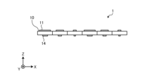
- FIG. 1 is a diagram for explaining an overview of a radio wave control plate according to a first embodiment.
- FIG. 2 is a diagram for explaining warping of the radio wave control plate according to the first embodiment.
- FIG. 3 is a diagram showing an example of the configuration of a unit structure according to the first embodiment.
- FIG. 4 is a diagram for explaining a method of imparting a warp to the radio wave control plate according to the second embodiment.
- FIG. 5 is a diagram showing an example of the configuration of a radio wave control panel according to the third embodiment.
- FIG. 6 is a diagram for explaining the relationship between the thickness and tolerance of the unit feature according to the fifth embodiment.
- an XYZ Cartesian coordinate system is set, and the positional relationship of each part is explained with reference to this XYZ Cartesian coordinate system.
- the direction parallel to the X-axis in a horizontal plane is defined as the X-axis direction
- the direction parallel to the Y-axis in the horizontal plane perpendicular to the X-axis is defined as the Y-axis direction
- the direction parallel to the Z-axis perpendicular to the horizontal plane is defined as the Z-axis direction.
- the plane containing the X-axis and Y-axis will be appropriately referred to as the XY plane
- the plane containing the X-axis and Z-axis will be appropriately referred to as the XZ plane
- the plane containing the Y-axis and Z-axis will be appropriately referred to as the YZ plane.
- the XY plane is parallel to the horizontal plane.
- the XY plane, XZ plane, and YZ plane are perpendicular to each other.
- Fig. 1 is a diagram for explaining the overview of the radio wave control plate according to the first embodiment.
- the radio wave control plate 1 is a plate-shaped member configured to be able to reflect or transmit (refract) radio waves transmitted by a base station. For example, when the radio wave control plate 1 receives radio waves transmitted by a base station, it is configured to reflect or refract the radio waves at a predetermined angle.
- the radio wave control plate 1 can be configured, for example, from a metamaterial that changes the phase of the incident wave.
- the radio wave control plate 1 includes, for example, unit structure 10A, unit structure 10B, unit structure 10C, unit structure 10D, unit structure 10E, unit structure 10F, unit structure 10G, unit structure 10H, and unit structure 10I.
- unit structure 10A unit structure 10B, unit structure 10C, unit structure 10D, unit structure 10E, unit structure 10F, unit structure 10G, unit structure 10H, and unit structure 10I.
- Unit structures 10A to 10I may be formed on a substrate.
- the substrate may be, for example, a dielectric substrate formed of a dielectric material.
- the substrate may have, for example, but is not limited to, a rectangular shape.
- Unit structures 10A to 10I may be arranged two-dimensionally on the substrate.
- the unit structures 10A are arranged along the Y-axis direction on the top row of the radio wave control plate 1.
- the unit structures 10B are arranged along the Y-axis direction on the row below the row in which the unit structures 10A are arranged.
- the unit structures 10C are arranged along the Y-axis direction on the row below the row in which the unit structures 10B are arranged.
- the unit structures 10D are arranged along the Y-axis direction on the row below the row in which the unit structures 10C are arranged.
- the unit structures 10E are arranged along the Y-axis direction on the row below the row in which the unit structures 10D are arranged.
- the unit structures 10F are arranged along the Y-axis direction on the row below the row in which the unit structures 10E are arranged.
- the unit structures 10G are arranged along the Y-axis direction on the row below the row in which the unit structures 10F are arranged.
- the unit structures 10H are arranged along the Y-axis direction on the row below the row in which the unit structures 10G are arranged.
- the unit structures 10I are arranged along the Y-axis direction on the row below the row in which the unit structures 10H are arranged.
- the amount of phase change can be made different for unit structures 10A to 10I by changing the size, shape, metal pattern, etc.
- Unit structures 10A to 10I are each formed to have a different amount of phase change.
- radio wave control plate 1 is configured to have a phase gradient along the X-axis.
- each of unit structures 10A to 10I is designed to have an ideal amount of phase change so as to reflect or refract radio waves in a desired direction. While this makes it possible to increase the electric field strength in a specific direction, it may result in a narrower beam width of the reflected or refracted wave. Therefore, in this disclosure, the radio wave control plate 1 is given a warp. When the radio wave control plate 1 is given a warp, the phase of the radio waves incident on each unit structure 10 becomes non-uniform, and the ideally designed amount of phase change is deviated. Therefore, by giving the radio wave control plate 1 a warp, the beam width of the reflected or refracted wave can be widened.
- FIG. 2 is a diagram for explaining the warping of the radio wave control plate according to the first embodiment.
- the radio wave control plate 1 has a warp that is concave at the center when viewed from the Y-axis direction. Specifically, the radio wave control plate 1 has a warp in a direction along the X-axis. That is, the radio wave control plate 1 has a warp along the direction in which the phase gradient is provided.
- the amount of warp L2 is, for example, about 1% with respect to the X-axis direction (phase gradient direction) of the radio wave control plate 1, but is not limited to this.
- the radio wave control plate 1 may have a warp that is concave at the center when viewed from the X-axis direction.
- Fig. 3 is a diagram showing a configuration example of the unit structure according to the first embodiment.
- the unit structure 10 has a first resonator 11, a second resonator 12, a third resonator 13, a fourth resonator 14, a first reference conductor 21, a second reference conductor 22, a third reference conductor 23, a first dielectric layer 31, a second dielectric layer 32, a third dielectric layer 33, a fourth dielectric layer 34, a fifth dielectric layer 35, and a sixth dielectric layer 36.
- the first resonator 11 is a resonator made of a conductive material (metallic material).
- the first resonator 11 is formed on the top surface of the unit structure 10.
- the top surface is also called the surface.
- the first resonator 11 is also called the first metallic element.
- the second resonator 12 and the third resonator 13 are resonators made of conductive materials.
- the second resonator 12 and the third resonator 13 are formed inside the unit structure 10.
- the fourth resonator 14 is a resonator made of a conductive material.
- the fourth resonator 14 is formed on the bottom surface of the unit structure 10.
- the bottom surface is also called the back surface.
- the fourth resonator 14 is also called the second metal element.
- the first reference conductor 21 is a ground conductor made of a conductive material.
- the first reference conductor 21 is formed inside the unit structure 10.
- the first reference conductor 21 is formed between the first resonator 11 and the second resonator 12.
- the first resonator 11 and the second resonator 12 are magnetically or capacitively connected via the first reference conductor 21.
- the first reference conductor 21 is a coupling adjustment conductor that adjusts the strength of coupling between the first resonator 11 and the second resonator 12.
- the second reference conductor 22 is a ground conductor made of a conductive material.
- the second reference conductor 22 is formed inside the unit structure 10.
- the second reference conductor 22 is formed between the second resonator 12 and the third resonator 13.
- the second resonator 12 and the third resonator 13 are magnetically or capacitively connected via the second reference conductor 22.
- the second reference conductor 22 is a coupling adjustment conductor that adjusts the strength of coupling between the second resonator 12 and the third resonator 13.
- the third reference conductor 23 is a ground conductor made of a conductive material.
- the third reference conductor 23 is formed inside the unit structure 10.
- the third reference conductor 23 is formed between the third resonator 13 and the fourth resonator 14.
- the third resonator 13 and the fourth resonator 14 are magnetically or capacitively connected via the third reference conductor 23.
- the third reference conductor 23 is a coupling adjustment conductor that adjusts the strength of coupling between the third resonator 13 and the fourth resonator 14.
- the first dielectric layer 31 is a dielectric substrate located between the first resonator 11 and the first reference conductor 21.
- the first dielectric layer 31 has a core layer 311 and a prepreg layer 312.
- the second dielectric layer 32 is a dielectric substrate located between the first reference conductor 21 and the second resonator 12.
- the second dielectric layer 32 has a core layer 321 and a prepreg layer 322.
- the third dielectric layer 33 is a dielectric substrate located between the second resonator 12 and the second reference conductor 22.
- the third dielectric layer 33 has a core layer 331 and a prepreg layer 332.
- the fourth dielectric layer 34 is a dielectric substrate located between the second reference conductor 22 and the third resonator 13.
- the fourth dielectric layer 34 has a core layer 341 and a prepreg layer 342.
- the fifth dielectric layer 35 is a dielectric substrate located between the third resonator 13 and the third reference conductor 23.
- the fifth dielectric layer 35 has a core layer 351 and a prepreg layer 352.
- the sixth dielectric layer 36 is a dielectric substrate located between the third reference conductor 23 and the fourth resonator 14.
- the sixth dielectric layer 36 has a core layer 361 and a prepreg layer 362.
- the unit structure 10 has seven layers, including a first resonator 11, a second resonator 12, a third resonator 13, a fourth resonator 14, a first reference conductor 21, a second reference conductor 22, and a third reference conductor 23, but the present disclosure is not limited thereto.
- the radio wave control plate 1 has a warp. This causes the incident phase of the radio waves incident on the radio wave control plate 1 according to the first embodiment to be non-uniform compared to the incident phase of the radio waves incident on a radio wave control plate that does not have a warp. Therefore, in the first embodiment, the beam width of the reflected wave or refracted wave from the radio wave control plate 1 can be widened.
- the radio wave control plate 1 can widen the beam width of the reflected wave or refracted wave by having a warp in a direction having a phase gradient.
- the radio wave control plate 1 is configured to have a phase gradient along the X direction by changing the phase change amount of the unit structures 10A to 10I by changing the patterns of the first resonator 11 to the fourth resonator 14 of the unit structures 10A to 10I, for example. As shown in FIG.
- the thicknesses of the unit structures 10A to 10I may differ. The thicker the unit structure 10 is, the less likely it is to warp, and the thinner the unit structure 10 is, the more likely it is to warp.
- the unit structures 10A to 10I are arranged so that the radio wave control plate 1 has a warp in a direction having a phase gradient.
- FIG. 4 is a diagram for explaining a method of imparting warping to the radio wave control plate according to the second embodiment.
- unit structures 10A and 10B are arranged in region 51.
- Unit structures 10C are arranged in region 52.
- Unit structures 10D, 10E, and 10F are arranged in region 53.
- Unit structures 10G are arranged in region 54.
- Unit structures 10H and 10I are arranged in region 55.
- unit structure 10A, unit structure 10B, unit structure 10D, unit structure 10E, unit structure 10F, unit structure 10H, and unit structure 10I the area of the first resonator 11 and the fourth resonator 14 are small, so the average thickness is also small.
- the metal coverage rate of unit structure 10A, unit structure 10B, unit structure 10D, unit structure 10E, unit structure 10F, unit structure 10H, and unit structure 10I is relatively low. Therefore, unit structures 10 that are prone to warping are arranged in regions 51, 53, and 55.
- the unit structures 10C and 10G have a large average thickness because the areas of the first resonator 11 and the fourth resonator 14 are large. In other words, the unit structures 10C and 10G have a relatively high metal coverage. Therefore, the unit structures 10 that are less likely to warp are arranged in the regions 52 and 54.
- unit structures 10 with a relatively low metal coverage and unit structures 10 with a relatively high metal coverage are periodically arranged along the X-axis direction.
- unit structures 10 that are prone to warping and unit structures 10 that are not prone to warping are periodically arranged along the X-axis direction.
- the second embodiment can provide a warp in the phase gradient direction of the radio wave control plate. This allows the second embodiment to more appropriately widen the beam width of the reflected wave or refracted wave from the radio wave control plate.
- the unit structures 10 having different phase change amounts are arranged along the X-axis direction of the radio wave control plate 1, but the present disclosure is not limited to this.
- the unit structures 10 having different phase change amounts may be arranged concentrically.
- the radio wave control plate 1 is configured to have a phase gradient along the radial direction of the concentric circles.
- unit structures 10 that are prone to warping and unit structures 10 that are less prone to warping are arranged periodically along the radial direction of the concentric circles.
- FIG. 5 is a diagram showing a configuration example of a radio wave control plate according to the third embodiment.
- the unit structures 10 arranged on the radio wave control plate 1 are formed so that the line widths of the first resonator 11 formed on the top surface and the fourth resonator 14 formed on the bottom surface are different.
- the radio wave control plate 1 can have a concave warp when viewed from the Y-axis direction.
- the first resonator 11 and the fourth resonator 14 are formed with different line widths depending on whether the line width is 0.3 mm or less or exceeds 0.3 mm. Specifically, when the line width of the first resonator 11 is 0.3 mm or less, the line width of the fourth resonator 14 is set to a range of X ⁇ 0.05 mm or less, where the line width of the first resonator 11 is X mm. Also, when the line width of the first resonator 11 exceeds 0.3 mm, the line width of the fourth resonator 14 is set to a range of X ⁇ 0.1 mm or less.
- the first resonator 11 and the fourth resonator 14 are formed with different line widths.
- the configuration of the top and bottom surfaces of the unit structure is asymmetric.
- by changing the line widths of the first resonator 11 and the fourth resonator 14 to make the configuration of the top and bottom surfaces of the unit structure asymmetric it is possible to impart an appropriate warp to the radio wave control plate 1. Therefore, in the third embodiment, the beam width of the reflected wave or refracted wave from the radio wave control plate can be more appropriately widened.
- the unit structure 10 has a structure in which a plurality of resonators and a reference conductor are laminated, as shown in Fig. 3.
- the first resonator 11 formed on the top surface of the unit structure 10 and the fourth resonator 14 formed on the bottom surface are formed so as to be offset from each other in the XY plane when viewed from the Z-axis direction, thereby making the radio wave control plate 1 warp.
- the first resonator 11 and the fourth resonator 14 are formed so as to be offset in the XY plane when viewed from the Z-axis direction.
- the configuration of the top and bottom surfaces of the unit structure is asymmetric.
- the radio wave control plate 1 by offsetting the positions of the first resonator 11 and the fourth resonator 14 in the XY plane when viewed from the Z-axis direction to make the configuration of the top and bottom surfaces asymmetric, it is possible to give the radio wave control plate 1 an appropriate warp.
- the fourth embodiment can more appropriately widen the beam width of the reflected wave or refracted wave from the radio wave control plate.
- the unit structure 10 has a substrate thickness of D mm.
- the thickness of each unit structure 10 included in the radio wave control plate 1 is made non-uniform, thereby causing the radio wave control plate 1 to have a warp.
- the unit structures 10 are set to be non-uniform within the tolerance range according to the thickness of the substrate.
- the radio wave control plate 1 if the thickness of the substrate of the unit structures 10 is D and the tolerance is ⁇ D, the unit structures 10 are formed non-uniformly within the range of D ⁇ D.
- FIG. 6 is a diagram for explaining the relationship between the thickness and the tolerance of the unit structures according to the fifth embodiment.
- the thickness D corresponds to the tolerance ⁇ D.
- the tolerance ⁇ D according to the thickness D of the substrate is set according to the relationship shown in the table TB1, and the thickness of each unit structure 10 of the radio wave control plate 1 is set to be non-uniform.
- the thickness of each unit structure 10 is formed non-uniformly within the range of 0.1 ⁇ 0.03 mm in the radio wave control plate 1.
- the thickness of each unit structure 10 included in the radio wave control plate 1 is formed non-uniformly within a predetermined range.
- the radio wave control plate 1 can be appropriately warped. Therefore, the fifth embodiment can more appropriately widen the beam width of the reflected wave or refracted wave from the radio wave control plate.
Landscapes
- Aerials With Secondary Devices (AREA)
Priority Applications (1)
| Application Number | Priority Date | Filing Date | Title |
|---|---|---|---|
| JP2025521933A JPWO2024241881A1 (https=) | 2023-05-19 | 2024-05-08 |
Applications Claiming Priority (2)
| Application Number | Priority Date | Filing Date | Title |
|---|---|---|---|
| JP2023-083300 | 2023-05-19 | ||
| JP2023083300 | 2023-05-19 |
Publications (1)
| Publication Number | Publication Date |
|---|---|
| WO2024241881A1 true WO2024241881A1 (ja) | 2024-11-28 |
Family
ID=93589173
Family Applications (1)
| Application Number | Title | Priority Date | Filing Date |
|---|---|---|---|
| PCT/JP2024/017121 Ceased WO2024241881A1 (ja) | 2023-05-19 | 2024-05-08 | 電波制御板 |
Country Status (2)
| Country | Link |
|---|---|
| JP (1) | JPWO2024241881A1 (https=) |
| WO (1) | WO2024241881A1 (https=) |
Citations (4)
| Publication number | Priority date | Publication date | Assignee | Title |
|---|---|---|---|---|
| JP2009515397A (ja) * | 2005-11-03 | 2009-04-09 | サントル ナシオナル ドゥ ラ ルシェルシェサイアンティフィク(セエヌエールエス) | リフレクトアレイ及びミリメートル波レーダー |
| JP2013543283A (ja) * | 2010-03-19 | 2013-11-28 | テールズ | 交差偏波補償を備えた反射器アレイアンテナおよびそのようなアンテナを製造するための方法 |
| JP2014527366A (ja) * | 2011-08-24 | 2014-10-09 | マイクロソフト コーポレーション | メタマテリアル及びアンテナシステム |
| JP2021027468A (ja) * | 2019-08-05 | 2021-02-22 | 電気興業株式会社 | ポスト付きメタサーフェスアンテナ |
-
2024
- 2024-05-08 WO PCT/JP2024/017121 patent/WO2024241881A1/ja not_active Ceased
- 2024-05-08 JP JP2025521933A patent/JPWO2024241881A1/ja active Pending
Patent Citations (4)
| Publication number | Priority date | Publication date | Assignee | Title |
|---|---|---|---|---|
| JP2009515397A (ja) * | 2005-11-03 | 2009-04-09 | サントル ナシオナル ドゥ ラ ルシェルシェサイアンティフィク(セエヌエールエス) | リフレクトアレイ及びミリメートル波レーダー |
| JP2013543283A (ja) * | 2010-03-19 | 2013-11-28 | テールズ | 交差偏波補償を備えた反射器アレイアンテナおよびそのようなアンテナを製造するための方法 |
| JP2014527366A (ja) * | 2011-08-24 | 2014-10-09 | マイクロソフト コーポレーション | メタマテリアル及びアンテナシステム |
| JP2021027468A (ja) * | 2019-08-05 | 2021-02-22 | 電気興業株式会社 | ポスト付きメタサーフェスアンテナ |
Also Published As
| Publication number | Publication date |
|---|---|
| JPWO2024241881A1 (https=) | 2024-11-28 |
Similar Documents
| Publication | Publication Date | Title |
|---|---|---|
| CN114597665B (zh) | 一种透射超表面阵列 | |
| WO2017032184A1 (en) | Metamaterial-based transmitarray for multi-beam antenna array assemblies | |
| JP6888671B2 (ja) | アンテナモジュール及び通信装置 | |
| US10826148B2 (en) | Ridge waveguide and array antenna apparatus | |
| JPH04354402A (ja) | 平面アンテナ | |
| US12341253B2 (en) | Antenna module and array antenna | |
| CN110729568B (zh) | 一种圆柱面共形超表面透镜天线 | |
| US11349184B2 (en) | Phase shifter including first and second boards having rails thereon and configured to be rotatable with respect to each other and an antenna formed therefrom | |
| JP6973626B2 (ja) | 無線通信装置 | |
| WO2024241881A1 (ja) | 電波制御板 | |
| CN112003024B (zh) | 温度调控二维全向金属-介质复合隐身器件及制作方法 | |
| US10923832B2 (en) | Co-construction antenna module | |
| US11527494B2 (en) | Module and electronic apparatus | |
| CN120691122A (zh) | 一种实现准无衍射波束赋形与扫描的天线 | |
| WO2024225042A1 (ja) | 電波制御板 | |
| CN111129761B (zh) | 一种双频段透射型天线 | |
| CN110931983B (zh) | 一种用于平面双极化毫米波宽带频率选择表面 | |
| US12412984B2 (en) | Antenna apparatus with floating patch | |
| WO2024262517A1 (ja) | 電波制御板および複合共振器 | |
| WO2025004939A1 (ja) | 通信システム、および電波制御板の設置方法 | |
| WO2024162166A1 (ja) | 電波反射板 | |
| WO2024262500A1 (ja) | 電波制御板および複合共振器 | |
| CN214505776U (zh) | 一种传输阵列天线单元和传输阵列天线 | |
| JP6464124B2 (ja) | アンテナ装置 | |
| WO2024043073A1 (ja) | 電波反射板および複合共振器 |
Legal Events
| Date | Code | Title | Description |
|---|---|---|---|
| 121 | Ep: the epo has been informed by wipo that ep was designated in this application |
Ref document number: 24810889 Country of ref document: EP Kind code of ref document: A1 |
|
| ENP | Entry into the national phase |
Ref document number: 2025521933 Country of ref document: JP Kind code of ref document: A |
|
| NENP | Non-entry into the national phase |
Ref country code: DE |