WO2024236433A1 - 表示装置 - Google Patents
表示装置 Download PDFInfo
- Publication number
- WO2024236433A1 WO2024236433A1 PCT/IB2024/054541 IB2024054541W WO2024236433A1 WO 2024236433 A1 WO2024236433 A1 WO 2024236433A1 IB 2024054541 W IB2024054541 W IB 2024054541W WO 2024236433 A1 WO2024236433 A1 WO 2024236433A1
- Authority
- WO
- WIPO (PCT)
- Prior art keywords
- layer
- conductive layer
- insulating layer
- semiconductor layer
- transistor
- Prior art date
- Legal status (The legal status is an assumption and is not a legal conclusion. Google has not performed a legal analysis and makes no representation as to the accuracy of the status listed.)
- Ceased
Links
Images













Classifications
-
- G—PHYSICS
- G02—OPTICS
- G02F—OPTICAL DEVICES OR ARRANGEMENTS FOR THE CONTROL OF LIGHT BY MODIFICATION OF THE OPTICAL PROPERTIES OF THE MEDIA OF THE ELEMENTS INVOLVED THEREIN; NON-LINEAR OPTICS; FREQUENCY-CHANGING OF LIGHT; OPTICAL LOGIC ELEMENTS; OPTICAL ANALOGUE/DIGITAL CONVERTERS
- G02F1/00—Devices or arrangements for the control of the intensity, colour, phase, polarisation or direction of light arriving from an independent light source, e.g. switching, gating or modulating; Non-linear optics
- G02F1/01—Devices or arrangements for the control of the intensity, colour, phase, polarisation or direction of light arriving from an independent light source, e.g. switching, gating or modulating; Non-linear optics for the control of the intensity, phase, polarisation or colour
- G02F1/13—Devices or arrangements for the control of the intensity, colour, phase, polarisation or direction of light arriving from an independent light source, e.g. switching, gating or modulating; Non-linear optics for the control of the intensity, phase, polarisation or colour based on liquid crystals, e.g. single liquid crystal display cells
- G02F1/133—Constructional arrangements; Operation of liquid crystal cells; Circuit arrangements
- G02F1/136—Liquid crystal cells structurally associated with a semi-conducting layer or substrate, e.g. cells forming part of an integrated circuit
- G02F1/1362—Active matrix addressed cells
- G02F1/1368—Active matrix addressed cells in which the switching element is a three-electrode device
-
- G—PHYSICS
- G09—EDUCATION; CRYPTOGRAPHY; DISPLAY; ADVERTISING; SEALS
- G09F—DISPLAYING; ADVERTISING; SIGNS; LABELS OR NAME-PLATES; SEALS
- G09F9/00—Indicating arrangements for variable information in which the information is built-up on a support by selection or combination of individual elements
- G09F9/30—Indicating arrangements for variable information in which the information is built-up on a support by selection or combination of individual elements in which the desired character or characters are formed by combining individual elements
-
- H—ELECTRICITY
- H10—SEMICONDUCTOR DEVICES; ELECTRIC SOLID-STATE DEVICES NOT OTHERWISE PROVIDED FOR
- H10D—INORGANIC ELECTRIC SEMICONDUCTOR DEVICES
- H10D30/00—Field-effect transistors [FET]
- H10D30/60—Insulated-gate field-effect transistors [IGFET]
- H10D30/67—Thin-film transistors [TFT]
Definitions
- One aspect of the present invention relates to a semiconductor device.
- One aspect of the present invention relates to a transistor.
- One aspect of the present invention relates to a display device having a transistor.
- one embodiment of the present invention is not limited to the above technical field.
- Examples of technical fields of one embodiment of the present invention disclosed in this specification and the like include semiconductor devices, display devices, light-emitting devices, power storage devices, memory devices, electronic devices, lighting devices, input devices, input/output devices, driving methods thereof, and manufacturing methods thereof.
- a semiconductor device refers to any device that can function by utilizing semiconductor characteristics.
- One type of display device is a liquid crystal display device that uses liquid crystal elements as the display element.
- liquid crystal display devices that uses liquid crystal elements as the display element.
- active matrix type liquid crystal display devices in which pixel electrodes are arranged in a matrix and switching elements are connected to each pixel electrode, are used in a variety of devices such as smartphones, tablet terminals, monitors, televisions, and digital signage.
- Liquid crystal display devices are broadly divided into two types: transmissive and reflective.
- the larger the effective light-emitting area ratio (also called the aperture ratio) of a pixel the brighter the display can be, and this also leads to reduced power consumption, so there is a demand for improved aperture ratios.
- Patent Document 1 discloses a liquid crystal display device that uses transistors with metal oxide as the channel formation region to increase the aperture ratio.
- An object of one embodiment of the present invention is to provide a liquid crystal display device with a high aperture ratio.
- an object of the present invention is to provide a high-definition liquid crystal display device.
- an object of the present invention is to provide a liquid crystal display device with low power consumption.
- an object of the present invention is to provide a liquid crystal display device that can be driven at high speed.
- an object of the present invention is to provide a display device with high display quality.
- Another object of one embodiment of the present invention is to provide a transistor that can be miniaturized. Another object is to provide a transistor with good electrical characteristics. Another object is to provide a transistor with a short channel length. Another object is to provide a transistor that occupies a small area.
- One aspect of the present invention is a display device having a transistor, a liquid crystal element, and a first insulating layer.
- the transistor has a semiconductor layer, a gate insulating layer, a gate electrode, and a first conductive layer.
- the first insulating layer has a first side surface. The first side surface is located on the first conductive layer.
- the semiconductor layer has a portion that is in contact with the upper surface and the first side surface of the first conductive layer and is located on the first insulating layer.
- the gate insulating layer has a surface that faces the first side surface through the semiconductor layer.
- the gate electrode has a surface that faces the first side surface through the semiconductor layer and the gate insulating layer.
- the liquid crystal element has liquid crystal, a second conductive layer, and a semiconductor layer.
- the second conductive layer is located on the first insulating layer and has a portion that overlaps with the semiconductor layer.
- the semiconductor layer includes a metal oxide.
- the transistor has a semiconductor layer, a gate insulating layer, a gate electrode, and a first conductive layer.
- the first insulating layer has an opening that reaches the first conductive layer, and has a first side surface located within the opening.
- the semiconductor layer has a portion that is in contact with the upper surface and the first side surface of the first conductive layer and is located on the first insulating layer.
- the gate insulating layer has a surface that faces the first side surface through the semiconductor layer.
- the gate electrode has a surface that faces the first side surface through the semiconductor layer and the gate insulating layer.
- the liquid crystal element has liquid crystal, a second conductive layer, and a semiconductor layer.
- the second conductive layer is located on the first insulating layer and has a portion that overlaps with the semiconductor layer.
- the semiconductor layer includes a metal oxide.
- the first insulating layer preferably has a first insulating film and a second insulating film on the first insulating film.
- the second insulating film preferably contains more hydrogen than the first insulating film.
- the semiconductor layer is preferably provided in contact with the second insulating film.
- the first insulating film contains an oxide
- the second insulating film contains a nitride.
- the second conductive layer is located on the semiconductor layer and contains a metal oxide. It is preferable that the gate insulating layer has a portion located between the second conductive layer and the semiconductor layer.
- the second conductive layer is provided on the gate insulating layer.
- the second conductive layer has a portion that overlaps with the semiconductor layer via the gate insulating layer and the second insulating layer. Furthermore, it is preferable that the second conductive layer has a portion that overlaps with the gate electrode via the second insulating layer.
- the semiconductor layer has a portion that overlaps with the second conductive layer via the third insulating layer.
- the first insulating layer preferably has a first insulating film and a second insulating film on the first insulating film.
- the second conductive layer is preferably located on the second insulating film.
- the third insulating layer preferably contains more hydrogen than the first insulating film, and the semiconductor layer is preferably provided in contact with the third insulating layer.
- a liquid crystal display device with a high aperture ratio can be provided.
- a high-definition liquid crystal display device can be provided.
- a liquid crystal display device with low power consumption can be provided.
- a liquid crystal display device capable of high-speed operation can be provided.
- a display device with high display quality can be provided.
- a transistor that can be miniaturized. Or, it is possible to provide a transistor that has good electrical characteristics. Or, it is possible to provide a transistor that has a short channel length. Or, it is possible to provide a transistor that occupies a small area.
- a transistor, a display device, an electronic device, etc. having a novel configuration. According to one aspect of the present invention, it is possible to provide a highly reliable transistor, a display device, an electronic device, etc. According to one aspect of the present invention, it is possible to at least alleviate at least one of the problems of the prior art.
- 1A and 1B show examples of the configuration of a display device.
- 2A and 2B show examples of the configuration of a display device.
- 3A and 3B show examples of the configuration of a display device.
- 4A and 4B show examples of the configuration of a display device.
- 5A and 5B show examples of the configuration of a display device.
- 6A and 6B show examples of the configuration of a display device.
- 7A and 7B show examples of the configuration of a display device.
- 8A and 8B show examples of the configuration of a display device.
- 9A and 9B show examples of the configuration of a display device.
- 10A and 10B show examples of the configuration of a display device.
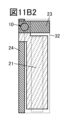
- 11A1 to 11B2 show configuration examples of the display device.
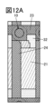
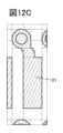
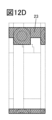
- 12A to 12E show configuration examples of the display device.
- FIG. 13 shows an example of the configuration of a display device.
- FIG. 14 shows an example of the configuration of a display device.
- FIG. 15 shows an example of the configuration of a display device.
- FIG. 16 shows an example of the configuration of a display device.
- FIG. 17 shows an example of the configuration of a display device.
- Fig. 18A is a block diagram of the display device, and Fig. 18B and Fig. 18C are circuit diagrams of the display device.
- 19A, 19C, and 19D are circuit diagrams of a display device, and Fig. 19B is a timing chart.
- FIG. 20 is a block diagram of the touch panel module.
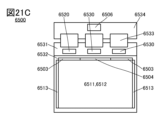
- 21A to 21C show configuration examples of a touch panel module.
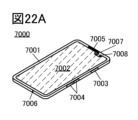
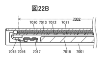
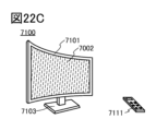
- 22A to 22F show configuration examples of electronic devices.
- electrically connected includes a connection via "something that has some kind of electrical action.”
- something that has some kind of electrical action is not particularly limited as long as it allows for the exchange of electrical signals between the connected objects.
- something that has some kind of electrical action includes electrodes or wiring, as well as switching elements such as transistors, resistive elements, coils, and other elements with various functions.
- the top surface shapes roughly match means that at least a portion of the contours of the stacked layers overlap. For example, this includes cases where the upper and lower layers are processed using the same mask pattern, or where a portion of the mask pattern is the same. However, strictly speaking, there are also cases where the contours do not overlap, and the upper layer is located inside the lower layer, or outside the lower layer, and in these cases, it may also be said that "the top surface shapes roughly match.”
- the top surface shape of a certain component refers to the contour shape of the component when viewed from a planar view.
- a planar view refers to a view from the normal direction of the surface on which the component is formed, or the surface of the support (e.g., substrate) on which the component is formed.
- film and “layer” are interchangeable.
- insulating layer may be interchangeable with the term “insulating film.”
- a display panel which is one aspect of a display device, has the function of displaying (outputting) images, etc. on a display surface. Therefore, a display panel is one aspect of an output device.
- a display panel having a connector such as an FPC (Flexible Printed Circuit) or TCP (Tape Carrier Package), attached to the substrate, or an IC mounted on the substrate using a method such as COG (Chip On Glass), may be referred to as a display panel module, display module, or simply a display panel.
- a connector such as an FPC (Flexible Printed Circuit) or TCP (Tape Carrier Package)
- COG Chip On Glass
- a touch panel which is one aspect of a display device, has a function of displaying an image or the like on a display surface, and a function as a touch sensor that detects when a detectable object such as a finger or stylus touches, presses, or approaches the display surface. Therefore, a touch panel is one aspect of an input/output device.
- a touch panel can also be called, for example, a display panel (or display device) with a touch sensor or a display panel (or display device) with a touch sensor function.
- a touch panel can also have a configuration that includes a display panel and a touch sensor panel. Alternatively, the touch panel can have a touch sensor function inside or on the surface of the display panel.
- a touch panel substrate on which a connector or IC is mounted may be referred to as a touch panel module, display module, or simply a touch panel.
- a transistor according to one embodiment of the present invention has a semiconductor layer, a gate insulating layer, a gate electrode, and a first electrode.
- the first electrode functions as one of a source electrode and a drain electrode.
- a part of the semiconductor layer functions as the other of the source electrode and the drain electrode.
- the portion of the semiconductor layer that functions as the other of the source electrode and drain electrode (also called the second electrode) is provided above the first electrode.
- An insulating layer that functions as a spacer is provided between the first electrode and the second electrode.
- the spacer has an opening that reaches the first electrode, and the semiconductor layer is provided in contact with the first electrode and the sidewall (also called the side surface) within the opening of the insulating layer.
- a gate insulating layer and a gate electrode are provided to cover the semiconductor layer.
- the source electrode and drain electrode are located at different heights, so the current flowing through the semiconductor layer flows in the height direction.
- the channel length direction can be said to have a height (vertical) component, so a transistor according to one embodiment of the present invention can also be called a VFET (Vertical Field Effect Transistor), vertical transistor, vertical channel transistor, etc.
- VFET Vertical Field Effect Transistor
- the above transistor allows the source electrode, semiconductor layer, and drain electrode to be stacked on top of each other, so it can occupy a much smaller area than a so-called planar type transistor (also called a lateral transistor, LFET (Lateral FET)) in which the semiconductor layer is arranged on a flat surface.
- planar type transistor also called a lateral transistor, LFET (Lateral FET)
- LFET Lateral FET
- the channel length of the transistor can be precisely controlled by the thickness of the insulating layer, the variation in channel length can be made extremely small compared to planar type transistors. Furthermore, by making the insulating layer thinner, transistors with extremely short channel lengths can be manufactured. For example, transistors with channel lengths of 2 ⁇ m or less, 1 ⁇ m or less, 500 nm or less, 300 nm or less, 200 nm or less, 100 nm or less, 50 nm or less, 30 nm or less, or 20 nm or less, and 5 nm or more, 7 nm or more, or 10 nm or more can be manufactured.
- transistors with extremely short channel lengths that could not be realized with conventional exposure equipment for mass production of flat panel displays (for example, minimum line width of about 2 ⁇ m or 1.5 ⁇ m).
- transistors with channel lengths of less than 10 nm without using extremely expensive exposure equipment used in cutting-edge LSI technology.
- the semiconductor layer it is preferable to use a metal oxide (also called oxide semiconductor) film having semiconductor properties, since this can achieve both high performance and high productivity.
- a metal oxide (also called oxide semiconductor) film having semiconductor properties since this can achieve both high performance and high productivity.
- an oxide semiconductor film having crystallinity since this can provide high reliability.
- the manufacturing process can be simplified compared to the case where a second electrode is separately provided.
- the contact portion between the semiconductor layer and the second electrode, which is necessary when a second electrode is separately provided, can be omitted, it is possible to further reduce the area occupied by the transistor.
- the second electrode can also function as a pixel electrode of the liquid crystal element. This makes it possible to realize a high-definition display device. Alternatively, the area that the transistor occupies with respect to the pixel can be reduced, making it possible to increase the aperture ratio (effective display area ratio) of the pixel.
- contact holes When using horizontal transistors, it is necessary to provide contact holes to connect the source or drain electrode of the transistor to the pixel electrode. Furthermore, depending on the transistor configuration, contact holes are also used to connect the source or drain electrode to the semiconductor layer. Due to the uneven shape caused by these contact holes, the alignment of the liquid crystal is disturbed in the contact holes and the areas nearby, making them unusable for display. This was one of the reasons why the aperture ratio of pixels could not be increased.
- the semiconductor layer of the transistor also serves as a pixel electrode, eliminating the need for an interlayer insulating film and a contact hole that are necessary when using a horizontal transistor, and thus increasing the aperture ratio of the pixel. Furthermore, as described above, the absence of a contact portion between the semiconductor layer of the transistor and the second electrode allows the aperture ratio to be further increased.
- Liquid crystal elements can be of various configurations. Typically, they can be transmissive liquid crystal display devices having liquid crystal elements in VA (Vertical Alignment) mode, FFS (Fringe Field Switching) mode, IPS (In-Plane Switching) mode, or the like. In addition to transmissive liquid crystal display devices, they can also be reflective or semi-transmissive.
- VA Vertical Alignment
- FFS Flexible Field Switching
- IPS In-Plane Switching
- Fig. 1A is a schematic top view of a portion of a pixel of a display device.
- Fig. 1B is a schematic cross-sectional view corresponding to dashed line A1-A2 in Fig. 1A.
- some components e.g., insulating layers
- some films are cut out in order to make the laminated structure easier to see.
- the display device of one embodiment of the present invention is a liquid crystal display device having a transistor 10 and a liquid crystal element 30 between a substrate 11 and a substrate 12.
- transistor 10 is provided at the intersection of conductive layer 23 and conductive layer 24.
- Conductive layer 23 functions as a scanning line, and a part of it functions as the gate electrode of transistor 10.
- Conductive layer 24 functions as a signal line, and a part of it functions as one of the source electrode and drain electrode of transistor 10.
- the transistor 10 is provided on a substrate 11 and has a semiconductor layer 21, an insulating layer 22, a conductive layer 23, and a conductive layer 24.
- the insulating layer 22 functions as a gate insulating layer.
- the liquid crystal element 30 also has a semiconductor layer 21 that functions as a pixel electrode, a conductive layer 32 that functions as a common electrode, and liquid crystal 33.
- the conductive layer 32 is provided between the semiconductor layer 21 and the liquid crystal 33. As shown in FIG. 1A, the conductive layer 32 has a slit that overlaps with the semiconductor layer 21.
- the liquid crystal element 30 shown in FIG. 1A is a liquid crystal element to which the FFS mode is applied.
- a part of the semiconductor layer 21 functions as a channel formation region, and another part functions as the other of the source electrode and drain electrode.
- a part of the part of the semiconductor layer 21 that functions as the other of the source electrode and drain electrode functions as a pixel electrode.
- a conductive layer 24 is provided on the substrate 11, and insulating layers 29a, 28, and 29b are provided in this order to cover the conductive layer 24.
- An opening 20 is provided in insulating layers 29b, 28, and 29a, reaching the conductive layer 24.
- the side walls (side surfaces) of insulating layers 29b, 28, and 29a at the opening 20 overlap the conductive layer 24.
- the semiconductor layer 21 contacts the upper surface of the conductive layer 24 located at the bottom of the opening 20, the side of the insulating layer 29a in the opening 20, the side of the insulating layer 28, the side of the insulating layer 29b, and the upper surface of the insulating layer 29b.
- the portion of the semiconductor layer 21 in contact with the conductive layer 24 functions as one of the source region and the drain region.
- the portion of the semiconductor layer 21 in contact with the insulating layer 29b can also be said to function as the other of the source region and the drain region.
- the region of the semiconductor layer 21 between these (particularly the region in contact with the insulating layer 28) functions as a region where a channel is formed (channel formation region). It is preferable that the region of the semiconductor layer 21 in contact with the insulating layer 29a and the region in contact with the insulating layer 29b have a higher carrier concentration and lower resistance than the channel formation region.
- An insulating layer 22 that functions as a gate insulating layer is provided to cover the insulating layer 29b and the semiconductor layer 21.
- a conductive layer 23 that functions as a gate electrode is further provided to cover the insulating layer 22.
- the semiconductor layer 21 has a portion that contacts the side of the insulating layer 28 and functions as a channel formation region.
- the insulating layer 22 has a portion (surface) that faces the side of the insulating layer 28 via the semiconductor layer 21.
- the conductive layer 23 also has a portion (surface) that faces the side of the insulating layer 28 via the semiconductor layer 21 and the insulating layer 22.
- the interface between the semiconductor layer 21 and the insulating layer 22 and the interface between the insulating layer 22 and the conductive layer 23 have portions that are parallel to the side of the insulating layer 28.
- An insulating layer 25 is provided to cover the insulating layer 22 and the conductive layer 23 and function as a protective layer. Furthermore, a conductive layer 32 that functions as a common electrode and an insulating layer 46 that functions as a spacer are provided on the insulating layer 25.
- a photosensitive resin can be used as the insulating layer 46.
- the insulating layer 46 can be formed by forming a photosensitive resin on the insulating layer 25, exposing it to light, and developing it.
- the photosensitive resin can be a resin having either negative or positive photosensitivity.
- the insulating layer 46 has the function of controlling the distance between the substrate 11 and the substrate 12 and controlling the thickness of the liquid crystal 33. Furthermore, it is preferable that the insulating layer 46 is provided so as to fill the depression in the upper surface of the insulating layer 25 caused by the opening 20. By providing the insulating layer 46 so as to overlap the transistor 10, it is possible to prevent a decrease in the aperture ratio caused by providing the insulating layer 46.
- the area of the transistor 10 in a planar view is smaller than that of a horizontal transistor, the area of the insulating layer 46 disposed in the area overlapping with the transistor 10 is also small. Therefore, if the strength as a spacer is insufficient, it is preferable to dispose the insulating layer 46 in all subpixels. This makes it possible to ensure sufficient strength even with an insulating layer 46 having a small area.
- the insulating layer 46 is provided on the substrate 11 side, but it may be provided on the substrate 12 side.
- the alignment film 41 may be provided in contact with the portion of the insulating layer 25 that overlaps with the transistor 10.
- the insulating layer 46 may be provided on both the substrate 11 side and the substrate 12 side.
- the conductive layer 32 which functions as a common electrode, has a portion that overlaps with the semiconductor layer 21 via the insulating layer 25 and the insulating layer 22.
- the portion where the conductive layer 32, the insulating layer 25, the insulating layer 22, and the semiconductor layer 21 are stacked functions as a storage capacitance of the pixel.
- the conductive layer 32 and the semiconductor layer 21 function as a pair of electrodes of the capacitance
- the insulating layer 25 and the insulating layer 22 function as a dielectric of the capacitance.
- the conductive layer 32 has a slit in a part of the area overlapping the semiconductor layer 21, and an opening in the area overlapping the opening 20.
- an alignment film 41 is provided covering the conductive layer 32, the insulating layer 46, and the insulating layer 25.
- a part of the semiconductor layer 21 of the transistor 10 serves as both the other of the source electrode and drain electrode of the transistor 10 and the pixel electrode of the liquid crystal element 30.
- the pixel electrode of the liquid crystal element 30 is required to have light-transmitting properties.
- silicon when silicon is used for the semiconductor layer 21, silicon has the property of absorbing part of visible light, and silicon that is further supplied with a dopant and has a low resistance is more likely to absorb visible light.
- an oxide semiconductor that has a higher light-transmitting property than silicon is suitable for the semiconductor used for the semiconductor layer 21.
- the alignment film 42 may have a portion that contacts alignment film 41 in a portion that overlaps with insulating layer 46. Note that either or both of alignment films 41 and 42 may not be provided if they are not required.
- the portion where the light-shielding layer 44 is provided becomes a non-light-emitting region.
- the light-shielding layer 44 can be provided in the region covering the transistor 10, the conductive layer 23, and the conductive layer 24.
- the area of the non-light-emitting region where the light-shielding layer 44 is provided can be significantly reduced compared to the conventional case.
- the colored layer 43 can also be called a color filter, and converts light from a light source such as a backlight into light exhibiting a specific color.
- a full-color display can be achieved by applying colored layers 43 corresponding to red, green, and blue to each pixel (sub-pixel) as the colored layer. It is preferable to provide pixels (sub-pixels) corresponding to colors such as yellow and white in addition to these three colors, as this reduces power consumption. In the case of white pixels, a configuration without providing a color filter to the pixel can be adopted.
- blue or purple light may be used as the light source, and a color conversion material that converts the blue or purple light to another color (e.g., red, green, etc.) may be applied to the colored layer 43.
- the color conversion material may be a fluorescent material, a phosphorescent material, or a resin material with quantum dots dispersed therein.
- the colored layer 43 has a laminated structure of a color conversion material and a color filter from the backlight side so that the light that passes through the color conversion material is absorbed.
- the insulating layer 45 functions as an overcoat that prevents the components contained in the colored layer 43, etc. from diffusing into the liquid crystal 33.
- the insulating layer 45 also functions as a planarizing film.
- the insulating layer 45 can be formed using an organic resin that is translucent.
- Substrate 11 and substrate 12 are bonded together by an adhesive layer (not shown) that is provided outside the display section.
- the distance between substrate 11 and substrate 12 is controlled by insulating layer 46, which functions as a spacer.
- a method is shown in which the pixel electrode and common electrode of the liquid crystal element 30 are arranged on the substrate 11 side, and an electric field is applied to the liquid crystal 33 in a direction perpendicular to the thickness direction.
- the method of arranging the electrodes is not limited to this, and a method of applying an electric field to the liquid crystal 33 in a direction parallel to the thickness direction may also be used.
- the display device can be a normally black type liquid crystal display device, for example, a transmissive type liquid crystal display device that employs a vertical alignment (VA) mode.
- VA vertical alignment
- MVA Multi-Domain Vertical Alignment
- PVA Pulned Vertical Alignment
- ASV Advanced Super View
- the liquid crystal element 30 can be a liquid crystal element to which various modes are applied.
- liquid crystal elements to which the TN (Twisted Nematic) mode, IPS mode, ASM (Axially Symmetric Aligned Micro-cell) mode, OCB (Opticaly Compensated Birefringence) mode, FLC (Ferroelectric Liquid Crystal) mode, AFLC (Anti Ferroelectric Liquid Crystal) mode, ECB (Electrically Controlled Birefringence) mode, guest host mode, etc. can be applied.
- the liquid crystal display device is a display device that controls the transmission or non-transmission of light by utilizing the optical modulation action of polarized light and liquid crystal.
- the optical modulation action of liquid crystal is controlled by an electric field (including a horizontal electric field, a vertical electric field, or an oblique electric field) applied to the liquid crystal.
- Examples of liquid crystals that can be used in liquid crystal elements include thermotropic liquid crystals, low molecular weight liquid crystals, polymer liquid crystals, polymer dispersed liquid crystals (PDLC: Polymer Dispersed Liquid Crystal), polymer network liquid crystals (PNLC: Polymer Network Liquid Crystal), ferroelectric liquid crystals, and antiferroelectric liquid crystals.
- liquid crystal materials exhibit cholesteric phases, smectic phases, cubic phases, chiral nematic phases, isotropic phases, and the like, depending on the conditions.
- positive liquid crystals or negative liquid crystals may be used as the liquid crystal material, and the most suitable liquid crystal material may be used depending on the mode or design to be applied.
- a polarizing plate is provided on each of the outer surfaces of substrate 11 and substrate 12. Furthermore, a backlight is provided on the outer side of substrate 11. In this case, the substrate 12 side becomes the display surface side.
- the semiconductor layer 21 preferably comprises a metal oxide (oxide semiconductor) having optical transparency.
- metal oxides examples include In oxide, Ga oxide, and Zn oxide.
- the metal oxide preferably contains at least In or Zn.
- the metal oxide preferably contains at least In or Ga.
- the metal oxide preferably contains two or three elements selected from In, element M, and Zn.
- the element M is a metal element or semimetal element that has a high bond energy with oxygen, for example, a metal element or semimetal element that has a higher bond energy with oxygen than In.
- Specific examples of element M include Al, Ga, Sn, Y, Ti, V, Cr, Mn, Fe, Co, Ni, Zr, Mo, Hf, Ta, W, La, Ce, Nd, Mg, Ca, Sr, Ba, B, Si, Ge, and Sb.
- the element M of the metal oxide is preferably one or more of the above elements, particularly preferably one or more selected from Al, Ga, Y, and Sn, and more preferably Ga.
- a metal oxide having In, M, and zinc may be referred to as In-M-Zn oxide.
- metal elements and metalloid elements may be collectively referred to as "metal elements", and the "metal element” described in this specification may include metalloid elements.
- the metal oxide is an In-M-Zn oxide
- the atomic ratio of In in the In-M-Zn oxide is equal to or greater than the atomic ratio of M.
- the term "close composition" includes a range of ⁇ 30% of the desired atomic ratio.
- the atomic ratio of In in the In-M-Zn oxide may be less than the atomic ratio of M.
- the semiconductor layer 21 may be, for example, In-Zn oxide, In-Ga oxide, In-Sn oxide, In-Ti oxide, In-Ga-Al oxide, In-Ga-Sn oxide, In-Ga-Zn oxide, In-Sn-Zn oxide, In-Al-Zn oxide, In-Ti-Zn oxide, In-Ga-Sn-Zn oxide, In-Ga-Al-Zn oxide, etc.
- Ga-Zn oxide may also be used.
- the metal oxide may contain one or more metal elements with a large periodic number.
- metal elements with a large periodic number include metal elements belonging to the fifth period and metal elements belonging to the sixth period. Specific examples of such metal elements include Y, Zr, Ag, Cd, Sn, Sb, Ba, Pb, Bi, La, Ce, Pr, Nd, Pm, Sm, and Eu. Note that La, Ce, Pr, Nd, Pm, Sm, and Eu are called light rare earth elements.
- the metal oxide may also contain one or more nonmetallic elements.
- the field effect mobility of the transistor may be increased.
- nonmetallic elements include carbon, nitrogen, phosphorus, sulfur, selenium, fluorine, chlorine, bromine, and hydrogen.
- the metal oxide can be preferably formed by sputtering or atomic layer deposition (ALD).
- ALD atomic layer deposition
- the composition of the metal oxide after film formation may differ from the composition of the target.
- the zinc content in the metal oxide after film formation may decrease to about 50% compared to the target.
- the content of a certain metal element in a metal oxide refers to the ratio of the number of atoms of that element to the total number of atoms of the metal element contained in the metal oxide.
- the content of metal element X can be expressed as Ax / ( Ax + Ay + Az ).
- metal element X when the ratio of the numbers of atoms of metal element X, metal element Y , and metal element Z in the metal oxide (atomic ratio) is expressed as Bx :By: Bz , the content of metal element X can be expressed as Bx /( Bx + By + Bz ).
- a transistor with high reliability when a positive bias is applied can be obtained.
- a transistor with a small amount of variation in threshold voltage in a PBTS (Positive Bias Temperature Stress) test can be obtained.
- the Ga content it is possible to produce a transistor with high reliability against light.
- NBTIS Near Bias Temperature Illumination Stress
- a metal oxide in which the atomic ratio of Ga is equal to or greater than the atomic ratio of In has a larger band gap, and it is possible to reduce the amount of variation in threshold voltage in NBTIS testing of a transistor.
- the metal oxide becomes highly crystalline, and the diffusion of impurities in the metal oxide can be suppressed. This suppresses fluctuations in the electrical characteristics of the transistor, and increases reliability.
- the semiconductor layer 21 may have a laminated structure having two or more metal oxide layers.
- the two or more metal oxide layers of the semiconductor layer 21 may have the same or approximately the same composition.
- a laminated structure of metal oxide layers having the same composition for example, they can be formed using the same sputtering target, thereby reducing manufacturing costs.
- a laminated structure in which two or more oxide semiconductor layers having different compositions are laminated may also be used.
- the semiconductor layer 21 is preferably a crystalline metal oxide layer.
- a metal oxide layer having a CAAC (c-axis aligned crystal) structure, a polycrystalline (Poly-crystal) structure, a nanocrystalline (nc: nano-crystal) structure, or the like can be used.
- CAAC c-axis aligned crystal
- Poly-crystal polycrystalline
- nc nano-crystal
- the defect level density in the semiconductor layer 21 can be reduced, and a highly reliable semiconductor device can be realized.
- the CAAC structure is a crystal structure in which multiple microcrystals (typically multiple IGZO microcrystals) have a c-axis orientation, and in the a-b plane, the multiple microcrystals are connected without being oriented.
- the CAAC structure has fewer crystal grain boundaries and grains in the a-b plane than a polycrystalline structure, making it possible to realize a highly reliable semiconductor device.
- OS transistors have extremely high field-effect mobility compared to transistors using amorphous silicon.
- OS transistors have an extremely small source-drain leakage current in an off state (hereinafter also referred to as off-current), and can hold charge accumulated in a capacitor connected in series with the transistor for a long period of time.
- off-current extremely small source-drain leakage current in an off state
- the use of OS transistors can reduce the power consumption of a semiconductor device.
- OS transistors Compared to transistors using silicon (hereinafter referred to as Si transistors), OS transistors have a higher withstand voltage between the source and drain, so a high voltage can be applied between the source and drain of the OS transistor. Furthermore, when the transistor operates in the saturation region, the OS transistor can reduce the change in source-drain current in response to a change in gate-source voltage compared to Si transistors.
- OS transistors have small variations in electrical characteristics due to radiation exposure, i.e., they have high resistance to radiation, and therefore can be suitably used in environments where radiation may be present. It can also be said that OS transistors have high reliability against radiation.
- OS transistors can be suitably used in pixel circuits of X-ray flat panel detectors.
- OS transistors can also be suitably used in semiconductor devices used in outer space.
- radiation include electromagnetic radiation (e.g., X-rays and gamma rays) and particle radiation (e.g., alpha rays, beta rays, proton rays, and neutron rays).
- the semiconductor material that can be used for the semiconductor layer 21 is not limited to oxide semiconductors.
- a semiconductor made of a single element or a compound semiconductor can be used.
- semiconductors made of a single element include silicon (including single crystal silicon, polycrystalline silicon, microcrystalline silicon, and amorphous silicon) and germanium.
- compound semiconductors include gallium arsenide and silicon germanium.
- compound semiconductors include organic semiconductors, nitride semiconductors, and oxide semiconductors. These semiconductor materials may contain impurities as dopants.
- the semiconductor layer 21 may have a layered material that functions as a semiconductor.
- a layered material is a general term for a group of materials that have a layered crystal structure.
- a layered crystal structure is a structure in which layers formed by covalent or ionic bonds are stacked via bonds weaker than covalent or ionic bonds, such as van der Waals bonds.
- a layered material has high electrical conductivity within a unit layer, that is, high two-dimensional electrical conductivity.
- Examples of the layered material include graphene, silicene, and chalcogenides.
- Chalcogenides are compounds containing chalcogen (an element belonging to Group 16).
- Examples of the chalcogenides include transition metal chalcogenides and Group 13 chalcogenides.
- transition metal chalcogenides that can be used as the semiconductor layer of a transistor include molybdenum sulfide (representatively MoS 2 ), molybdenum selenide (representatively MoSe 2 ), molybdenum tellurium (representatively MoTe 2 ), tungsten sulfide (representatively WS 2 ), tungsten selenide (representatively WSe 2 ), tungsten tellurium (representatively WTe 2 ), hafnium sulfide (representatively HfS 2 ), hafnium selenide (representatively HfSe 2 ), zirconium sulfide (representatively ZrS 2 ), zirconium selenide (representatively ZrSe 2 ), and the like.
- the crystallinity of the semiconductor material used for the semiconductor layer 21 is not particularly limited, and any of an amorphous semiconductor, a single crystal semiconductor, and a semiconductor having crystallinity other than single crystal (a polycrystalline semiconductor, a microcrystalline semiconductor, or a semiconductor having a crystalline region in part) may be used.
- the use of a crystalline semiconductor is preferable because it can suppress deterioration of the transistor characteristics.
- the upper surface of the conductive layer 24 contacts the semiconductor layer 21.
- an oxide semiconductor is used as the semiconductor layer 21
- a metal that is easily oxidized such as aluminum
- an insulating oxide e.g. aluminum oxide
- the conductive layer 24 can be made of a transparent oxide conductive material.
- conductive oxides such as indium oxide, zinc oxide, In-Sn oxide, In-Zn oxide, In-W oxide, In-W-Zn oxide, In-Ti oxide, In-Ti-Sn oxide, In-Sn oxide containing silicon, and zinc oxide doped with gallium can be used.
- Conductive oxides containing indium are particularly preferred because of their high conductivity.
- a conductive material that absorbs or reflects a portion of visible light may be used.
- tantalum nitride, titanium nitride, nitrides containing titanium and aluminum, nitrides containing tantalum and aluminum, ruthenium oxide, ruthenium nitride, oxides containing strontium and ruthenium, oxides containing lanthanum and nickel, etc. may be used.
- titanium, ruthenium, tungsten, etc. may also be used.
- the insulating layer 22 functions as a gate insulating layer.
- an oxide semiconductor is used for the semiconductor layer 21, it is preferable to use an oxide insulating film for at least the film of the insulating layer 22 that is in contact with the semiconductor layer 21.
- an oxide insulating film for at least the film of the insulating layer 22 that is in contact with the semiconductor layer 21.
- silicon oxide, silicon oxynitride, aluminum oxide, aluminum oxynitride, hafnium oxide, hafnium oxynitride, gallium oxide, gallium oxynitride, yttrium oxide, yttrium oxynitride, and Ga-Zn oxide can be used.
- a nitride insulating film such as silicon nitride, silicon nitride oxide, aluminum nitride, or aluminum nitride oxide can also be used as the insulating layer 22.
- the insulating layer 22 may have a layered structure, and may have, for example, a layered structure having one or more oxide insulating films and one or more nitride insulating films.
- oxynitride refers to a material that contains more oxygen than nitrogen.
- Nitrogen oxide refers to a material that contains more nitrogen than oxygen.
- the conductive layer 23 functions as a gate electrode, and various conductive materials can be used.
- the conductive layer 23 can be formed using, for example, one or more of chromium, copper, aluminum, gold, silver, zinc, molybdenum, tantalum, titanium, tungsten, manganese, nickel, iron, cobalt, molybdenum, and niobium, or an alloy containing one or more of the above-mentioned metals.
- the conductive layer 23 may also be formed using nitrides and oxides that can be used for the conductive layer 24.
- the insulating layer 28 has a portion that contacts the semiconductor layer 21.
- an oxide semiconductor is used for the semiconductor layer 21, it is preferable to use an oxide for at least the portion of the insulating layer 28 that contacts the semiconductor layer 21 in order to improve the interface characteristics between the semiconductor layer 21 and the insulating layer 28.
- silicon oxide or silicon oxynitride can be suitably used.
- a film that releases oxygen when heated for the insulating layer 28 This allows oxygen to be supplied to the semiconductor layer 21 by the heat applied during the manufacturing process of the transistor 10, and oxygen vacancies in the semiconductor layer 21 can be reduced, thereby improving reliability.
- Methods for supplying oxygen to the insulating layer 28 include heat treatment in an oxygen atmosphere and plasma treatment in an oxygen atmosphere.
- Oxygen may also be supplied by forming an oxide film in an oxygen atmosphere on the upper surface of the insulating layer 28 by a sputtering method. The oxide film may then be removed.
- the insulating layer 28 is preferably formed by a deposition method such as a sputtering method or a plasma CVD method.
- a deposition method such as a sputtering method or a plasma CVD method.
- a gas containing hydrogen is not required as a deposition gas, and a film with an extremely low hydrogen content can be obtained. This makes it possible to suppress the supply of hydrogen to the semiconductor layer 21 and stabilize the electrical characteristics of the transistor 10.
- Insulating layers 29a and 29b are preferably made of a film through which oxygen does not easily diffuse. This makes it possible to prevent oxygen contained in insulating layer 28 from permeating through insulating layer 29a to the substrate 11 side due to heating, and from permeating through insulating layer 29b to the insulating layer 22 side. In other words, by sandwiching insulating layer 28 between insulating layers 29a and 29b, through which oxygen does not easily diffuse, the oxygen contained in insulating layer 28 can be trapped. This makes it possible to effectively supply oxygen to semiconductor layer 21.
- silicon nitride, silicon nitride oxide, silicon oxynitride, aluminum oxide, aluminum oxynitride, aluminum nitride, hafnium oxide, and hafnium aluminate can be used.
- silicon nitride and silicon nitride oxide have the characteristics of releasing little impurities (e.g., water and hydrogen) from themselves and being difficult for oxygen and hydrogen to permeate, and therefore can be suitably used as the insulating layer 29a and the insulating layer 29b.
- the insulating layer 29b does not easily diffuse oxygen, oxygen is not supplied to a portion of the semiconductor layer 21 that contacts the upper surface of the insulating layer 29b, resulting in a state of many oxygen vacancies. Therefore, in this portion, hydrogen in the semiconductor layer 21 combines with the oxygen vacancies to generate carriers, resulting in a low resistance state.
- the insulating layer 29b may have a laminated structure of an insulating film that is difficult for oxygen and hydrogen to penetrate from the insulating layer 28 side and an insulating film that releases hydrogen when heated. That is, a film that releases hydrogen when heated is provided on the side of the insulating layer 29b that contacts the semiconductor layer 21. This makes it possible to more effectively reduce the resistance of the part of the semiconductor layer 21 that contacts the insulating layer 29b.
- silicon nitride, silicon nitride oxide, silicon oxynitride, or silicon oxide formed to contain hydrogen can be used.
- a film that releases a lot of hydrogen can be formed by forming the film at a low temperature (for example, a temperature of 100°C to 400°C, preferably 100°C to 300°C) using a film forming method using a gas containing hydrogen (hydrogen gas or hydrogen compound gas) as the film forming gas, such as a film forming method such as a plasma CVD method.
- a gas containing hydrogen hydrogen gas or hydrogen compound gas
- a film forming method such as a plasma CVD method.
- the conductive layer 23 and the semiconductor layer 21 overlap with the insulating layer 22, and the conductive layer 24 and the semiconductor layer 21 overlap with the insulating layer 29a, the insulating layer 28, and the insulating layer 29b.
- the thickness of the insulating layer 22 is formed thinner than the thickness of the three layers of the insulating layer 29a, the insulating layer 28, and the insulating layer 29b, so that the driving voltage of the transistor 10 can be reduced.
- the thinner the insulating layer 22 the larger the parasitic capacitance between the semiconductor layer 21 and the conductive layer 23.
- the insulating layer 29a, the insulating layer 28, and the insulating layer 29b can be formed thicker than the insulating layer 22, the parasitic capacitance between the semiconductor layer 21 and the conductive layer 24 can be reduced. Therefore, as shown in FIG. 1A, it is preferable to arrange the semiconductor layer 21 so that the area overlapping with the conductive layer 23 is smaller than the area overlapping with the conductive layer 24. This makes it possible to realize a display device that can display at a high driving frequency even if the resolution is high.
- FIG. 2A shows an enlarged cross-section of transistor 10.
- the channel length L of the transistor 10 refers to the shortest distance between the portion of the semiconductor layer 21 that contacts the conductive layer 24 and the portion that contacts the top surface of the insulating layer 29b, as shown in FIG. 2A. The closer the side surfaces of the insulating layers 29a, 28, and 29b at the opening 20 are to the substrate surface, the shorter the channel length L becomes.
- the channel width W of the transistor 10 also coincides with the perimeter of the opening 20. As shown in FIG. 1A, when the top surface shape of the opening 20 is circular and its diameter is R, the channel width W of the transistor 10 coincides with the length of the circumference of the opening 20, which is ⁇ R. When the top surface shape of the opening 20 is circular, the transistor can have the smallest channel width W.
- the diameter of the opening 20 often changes in the depth direction.
- the average value of the diameter at the highest point of the insulating layer 28 in a cross-sectional view, the diameter at the lowest point, and the diameter at the midpoint between these three points can be used as the diameter of the opening 20.
- the diameter of the opening 20 may be any of the diameter at the highest point of the insulating layer 28, the diameter at the lowest point, or the diameter at the midpoint between these two points.
- the shape of the opening 20 is circular, but it is not limited to this and can be various shapes.
- it can be an ellipse, a rectangle with rounded corners, etc.
- It can also be a regular polygon such as an equilateral triangle, square, or regular pentagon, or a polygon other than a regular polygon.
- the channel width can be increased by making it a concave polygon, such as a star-shaped polygon, which is a polygon with at least one interior angle exceeding 180 degrees.
- the side surfaces of the insulating layer 28, the insulating layer 29a, and the insulating layer 29b in the opening 20 are inclined upward, so that they have a tapered shape.
- the angle ⁇ when the angle between the side surface of the insulating layer 28 in the opening 20 and the upper surface of the conductive layer 24 located at the bottom of the opening 20 is the angle ⁇ , for example, it is preferable that the angle ⁇ is 90 degrees or more and has a portion where it is 135 degrees or less, preferably 125 degrees or less, more preferably 120 degrees or less, and more preferably 110 degrees or less.
- the semiconductor layer 21 is also formed along the side surfaces of the openings in the insulating layers 29a, 28, and 29b.
- films formed using a film forming method such as sputtering or plasma CVD tend to be thinner on surfaces that are inclined or perpendicular to the substrate surface than on surfaces that are horizontal to the substrate surface. Therefore, when the semiconductor layer 21 is formed by sputtering, the thickness of the portion in contact with the insulating layer 28 may be thinner than the thickness of the portion in contact with the top surface of the conductive layer 24 and the thickness of the portion in contact with the top surface of the insulating layer 29b.
- the insulating layer 22 and the conductive layer 23 can be formed so that the thickness of the portions formed along the side surfaces of the openings in the insulating layer 28, etc., is thinner than the portions formed on the upper surfaces of the conductive layer 24 and the insulating layer 29b.
- a film of uniform thickness can be formed regardless of the inclination angle of the surface on which it is formed, so there may be little difference in thickness between the semiconductor layer 21, the insulating layer 22, the conductive layer 23, etc.
- a light-shielding conductive material for one or both of the conductive layers 23 and 24, it is possible to block light that reaches the channel formation region of the semiconductor layer 21, thereby improving the reliability of the transistor 10. In particular, it is possible to reduce the fluctuation in threshold voltage in the NBTIS test.
- a light-shielding conductive material for at least the conductive layer on the side where the backlight is provided.
- the semiconductor layer 21, the insulating layer 22, and the conductive layer 23 are provided to cover the entire opening 20 in a plan view, but this is not limiting.
- the semiconductor layer 21, the insulating layer 22, and the conductive layer 23 may be laminated along at least a portion of the side surface of the insulating layer 28.
- either one or both of the semiconductor layer 21 and the conductive layer 23 may be provided to cover a portion of the opening 20 and not cover the other portion.
- the opening 20 may be formed in a long and narrow groove (slit) shape, and either one or both of the semiconductor layer 21 and the conductive layer 23 may be configured to cover a portion of the groove-shaped opening 20 and not cover the other portion, or to straddle the groove-shaped opening 20.
- the display device of one embodiment of the present invention has such a configuration, making it possible to realize a liquid crystal display device with an extremely high aperture ratio.
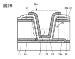
- FIG. 2B shows an example of a transistor 10a that can be formed on the same plane as transistor 10.
- Transistor 10a differs from transistor 10 primarily in that it has a conductive layer 31.
- the conductive layer 31 functions as the other of the source electrode and drain electrode of the transistor 10a.
- the conductive layer 31 is provided on the insulating layer 29b, and the semiconductor layer 21 is provided in contact with the upper surface of the conductive layer 31.
- the conductive layer 31 can be made of a conductive material similar to the conductive layer 24.
- the conductive layer 31 preferably has a lower resistance than the semiconductor layer 21.
- a relatively high resistance material such as a metal oxide
- Transistor 10 can be used as a transistor connected to a pixel electrode of a pixel. Meanwhile, transistor 10a can be used in a scanning line driving circuit, a signal line driving circuit, a protection circuit, and other circuits other than a pixel circuit.
- Transistor 10 and transistor 10a can be fabricated separately through the same process.
- a mask pattern for processing conductive layer 31 can be used to fabricate transistor 10a having conductive layer 31 and transistor 10 not having conductive layer 31.
- the configuration shown in FIG. 3A differs from the above-described configuration example mainly in that the shape of the conductive layer 32 is different.
- an opening is provided in a portion that overlaps with the opening 20 so that the conductive layer 32 does not overlap the opening 20, but in FIG. 3A, the conductive layer 32 is provided so as to overlap the opening 20.
- the conductive layer 32 has a portion that is located between the insulating layer 25 and the insulating layer 46.
- the conductive layer 32 By configuring the conductive layer 32 to cover the transistor 10 in this way, it can be used as a shield to prevent electrical noise input from the substrate 12 from being transmitted to the transistor 10. For example, when a touch sensor electrode is provided on the substrate 12, electrical noise caused by a signal applied to the electrode can be prevented from being transmitted to the transistor 10, the conductive layer 23 functioning as a scanning line, and the conductive layer 24 functioning as a signal line.
- the configuration shown in FIG. 3B differs from the above-described configuration example mainly in that the conductive layer 32 is located closer to the substrate 11 than the semiconductor layer 21 .
- a conductive layer 32 is provided on the insulating layer 29b, an insulating layer 34 is provided covering the conductive layer 32, and a semiconductor layer 21 is provided on the insulating layer 34.
- insulating layers 22, 25, and an alignment film 41 are provided covering the semiconductor layer 21.
- the portion where the semiconductor layer 21, the insulating layer 34, and the conductive layer 32 are stacked functions as a storage capacitor, so part of the insulating layer 34 functions as a dielectric for the capacitor.
- the insulating layer 34 it is preferable to use an insulating material with a higher dielectric constant than, for example, silicon oxide.
- an insulating material that can be used for the insulating layer 29a, etc. can be used.
- the insulating layer 34 that functions as the dielectric of the storage capacitor can be formed separately from the insulating layers 22 and 25, allowing the thickness and material to be optimized.
- a film that releases hydrogen when heated as described above for at least the portion of the insulating layer 34 that contacts the semiconductor layer 21. This allows the portion of the semiconductor layer 21 that functions as a pixel electrode to have a low resistance.
- FIG. 4A differs from the above-described configuration example mainly in that the conductive layer 32 is provided on and in contact with the insulating layer 22.
- Insulating layer 22 has a portion that contacts conductive layer 23 and a portion that contacts conductive layer 32. In other words, it can be said that conductive layer 23 and conductive layer 32 are formed on the same surface on which they are formed (specifically, the upper surface of insulating layer 22).
- the conductive layer 23 and the conductive layer 32 may be made of the same conductive film having light transmission properties, but it is preferable to use a conductive material having lower resistance than the conductive layer 32 for the conductive layer 23. In this case, it does not matter which of the conductive layer 23 and the conductive layer 32 is formed first.
- the conductive layer 23 may be a laminate of a conductive film having light transmission properties used for the conductive layer 32 and a conductive film having low resistance.
- a part of the conductive layer 32 may overlap the conductive layer 23. This allows the conductive layer 23 and the conductive layer 32 to be processed without problems even if the etching selectivity between the conductive layer 23 and the conductive layer 32 cannot be increased.
- a resist mask may be formed so as to cover the part of the conductive film that overlaps with the conductive layer 23, and then the conductive film may be etched to form the conductive layer 32.
- FIG. 4B differs from the above-described configuration example mainly in that a conductive layer 26 is provided between the conductive layer 24 and the substrate 11.
- the conductive layer 24 when an oxide semiconductor is used for the semiconductor layer 21, it is preferable to use for the conductive layer 24 a conductive material that is resistant to oxidation, a conductive material that maintains low electrical resistance even when oxidized, or an oxide conductive material. Furthermore, since the conductive layer 24 also functions as a signal line, it is preferable that it has low resistance. Therefore, it is preferable to use a conductive material that is resistant to oxidation, a conductive material that maintains low electrical resistance even when oxidized, or an oxide conductive material for the portion of the conductive layer 24 that contacts the semiconductor layer 21, and a low-resistance conductive material for the other portions.
- conductive layer 24 is laminated on conductive layer 26 and processed so that their ends are roughly aligned, but this configuration is not limiting as long as conductive layer 26 and conductive layer 24 are electrically connected.
- conductive layer 26 may be provided in contact with the upper or lower surface of conductive layer 24 in a portion of conductive layer 24 other than the portion in contact with semiconductor layer 21.
- ⁇ Modification 5 ⁇ The configuration shown in FIG. 5A is an example in which a VA mode liquid crystal element 30 is applied.
- the conductive layer 32 is provided on the substrate 12 side. More specifically, the conductive layer 32 is provided between the insulating layer 45 and the alignment film 42.
- a conductive layer 35 is provided between the substrate 11 and the insulating layer 29a.
- the conductive layer 35 is preferably formed by processing the same conductive film as the conductive layer 24, and has light-transmitting properties.
- a storage capacitance is formed by the conductive layer 35, the semiconductor layer 21, and the insulating layers 29a, 28, and 29b provided between them.
- the conductive layer 35 is preferably formed in the same process as the conductive layer 24, since this allows a storage capacitance to be provided without increasing the number of manufacturing steps.
- FIG. 5B The configuration shown in FIG. 5B is an example in which an IPS mode liquid crystal element 30 is applied.
- the semiconductor layer 21 and the conductive layer 32 are each provided on the insulating layer 29b. In this case, it is preferable that the semiconductor layer 21 and the conductive layer 32 are formed by processing the same film.
- the semiconductor layer 21 and the conductive layer 32 each have a comb-like upper surface shape, and are arranged so that they interdigitate without touching each other.
- the semiconductor layer 21 and the conductive layer 32 are given different hatching patterns for ease of explanation.
- FIG. 6A the portion of the insulating layer 28 that overlaps with the liquid crystal element 30 has been removed by etching. That is, the configuration shown in FIG. 6A has a portion in which the conductive layer 35, insulating layer 29a, insulating layer 29b, and semiconductor layer 21 are stacked in this order. This allows the capacitance between the conductive layer 35 and the semiconductor layer 21 to be increased compared to the configuration illustrated in FIG. 5A. Furthermore, not providing the insulating layer 28 in the portion that functions as the liquid crystal element 30 not only increases the light transmittance, but also reduces the number of interfaces located on the path of the light from the light source, thereby suppressing the effects of interface reflection and interface scattering.
- not only the insulating layer 28 but also the portion of the insulating layer 29a that overlaps with the liquid crystal element 30 may be etched. This not only increases the capacitance between the conductive layer 35 and the semiconductor layer 21, but also improves the light transmittance and further suppresses the effects of interface reflection and interface scattering.
- the conductive layer 32 in FIG. 3B is formed from the same conductive film as the conductive layer 24. Furthermore, the portion of the insulating layer 28 that overlaps with the liquid crystal element 30 is removed by etching. This allows the conductive layer 24 and the conductive layer 32 to be manufactured in the same process, simplifying the process. Furthermore, as with the seventh modification, not providing the insulating layer 28 not only increases the light transmittance, but also suppresses the effects of interface reflection and interface scattering.
- either or both of insulating layer 22 and insulating layer 25 may have the portions overlapping with liquid crystal element 30 removed by etching.
- insulating layer 25 may not be provided if it is not necessary. This allows the electric field of semiconductor layer 21 and conductive layer 32 to be easily transmitted to liquid crystal 33, enabling high-speed operation of liquid crystal element 30. Furthermore, not only is the light transmittance in the portions overlapping with liquid crystal element 30 increased, but the effects of interface reflection and interface scattering can also be suppressed.
- the portion of either the insulating layer 29a or the insulating layer 29b that overlaps with the liquid crystal element 30 may be removed by etching. This also makes it easier for the electric field of the semiconductor layer 21 and the conductive layer 32 to be transmitted to the liquid crystal 33. Furthermore, it may be possible to increase the capacitance between the semiconductor layer 21 and the conductive layer 32.
- Figure 7B shows an example in which the portion of the insulating layer 29a that overlaps with the liquid crystal element 30 is removed by etching.
- FIG. 7A shows a case where both the semiconductor layer 21 and the conductive layer 32 have a comb-like top surface shape, but in FIG. 8A, only the semiconductor layer 21 is comb-like, and the semiconductor layer 21 and the conductive layer 32 overlap.
- This allows the capacitance between the semiconductor layer 21 and the conductive layer 32 to be used as a storage capacitance, and there is no need to provide a separate capacitive element, making it possible to realize a display device with a high aperture ratio.
- the portion of either or both of the insulating layer 22 and the insulating layer 25 that overlaps with the liquid crystal element 30 may be removed by etching, and the insulating layer 25 may not be provided if it is not necessary.
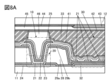
- FIG. 8B is a modification of the configurations shown in FIGS. 5B and 7A.
- FIG. 8B in the region where insulating layer 28 is not provided, insulating layers 29a and 29b are each removed by etching, and semiconductor layer 21 and conductive layer 32 are formed on the same surface.
- semiconductor layer 21 and conductive layer 32 are given different hatching patterns, but semiconductor layer 21 and conductive layer 32 may be formed by processing the same film.
- conductive layer 32 may be formed by processing the same conductive film as conductive layer 24.
- the portions of either or both of the insulating layer 22 and the insulating layer 25 that overlap the liquid crystal element 30 may be removed by etching, and the insulating layer 25 may not be provided if it is not necessary.
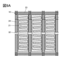
- FIG. 9A is a schematic top view of a pixel.
- three sub-pixels are clearly shown lined up.
- the three sub-pixels correspond to three colors, for example, red (R), green (G), and blue (B), and have the same configuration except that each sub-pixel has a colored layer that transmits light of the corresponding color and absorbs light of the other colors.
- the subpixels are provided corresponding to the intersections of the conductive layers 23 that function as scan lines and the conductive layers 24 that function as signal lines.
- the subpixels include a transistor 10, a part of the semiconductor layer 21 that functions as a pixel electrode, and a conductive layer 32 that functions as a common electrode.
- the transistor 10 is provided at the intersection of the conductive layers 23 and 24.
- FIG. 9A corresponds to the laminated structure illustrated in FIG. 3B, and is an example in which the conductive layer 32 functioning as a common electrode is located closer to the substrate 11 than the semiconductor layer 21 functioning as a pixel electrode.
- the semiconductor layer 21 in FIG. 9A is given a hatched pattern that allows the layers located below it (on the substrate 11 side) to be seen through.
- the semiconductor layer 21 has a comb-tooth shape in a plan view. As shown in FIG. 9A, it is preferable that the sides of the protruding portions of the comb-tooth-shaped semiconductor layer 21 are oblique to the extension direction of the conductive layers 23 and 24. The protruding portions of the semiconductor layer 21 are oriented symmetrically with respect to the extension direction of the conductive layer 24 (top-bottom symmetrical in the figure). This configuration can improve the viewing angle characteristics in terms of luminance and chromaticity of the display device.
- the semiconductor layer 21 has a comb-like shape in this example, it may have any shape as long as the portions where the semiconductor layer 21 and the conductive layer 32 are stacked and the portions where the semiconductor layer 21 is not provided on the conductive layer 32 are arranged alternately.
- the semiconductor layer 21 may have a shape having a plurality of openings.
- a part of the conductive layer 32 has a portion that overlaps with the conductive layer 24, and the conductive layer 32 is connected between the sub-pixels arranged in the extension direction of the conductive layer 23 by this portion.
- the conductive layer 32 is provided with a portion that overlaps with the conductive layer 24, rather than providing a portion that overlaps with the conductive layer 23, to connect the sub-pixels.
- the conductive layer 32 and the conductive layer 24 overlap via an insulating layer 28 or the like that functions as a spacer, so that the parasitic capacitance can be reduced compared to when the conductive layer 32 and the conductive layer 23 overlap.
- FIG. 9A it is preferable to make the overlapping area between the conductive layer 32 and the conductive layer 24 as small as possible, since this can further reduce the parasitic capacitance between them.
- the semiconductor layer 21 is arranged so that the area that it overlaps with the conductive layer 23 is smaller than the area that it overlaps with the conductive layer 24. This effectively reduces the parasitic capacitance between the semiconductor layer 21 and the conductive layer 23.
- FIG. 9B shows an example in which the top-bottom relationship between the semiconductor layer 21 and the conductive layer 32 is reversed compared to FIG. 9A. For example, this corresponds to the configuration shown in FIG. 3A.
- the hatching patterns of the semiconductor layer 21 and the conductive layer 32 are swapped from FIG. 9A to clearly show this.
- the conductive layer 32 has a plurality of slits (also called openings) that overlap the semiconductor layer 21.
- the long side directions of these slits are arranged so as to be oblique to the extension direction of the conductive layer 23 and the extension direction of the conductive layer 24. It is also preferable that the long side directions of the slits are symmetrical with respect to the extension direction of the conductive layer 24, with the center part of the semiconductor layer 21 as the boundary. This can improve the viewing angle characteristics.
- the configuration shown in FIG. 10A differs from the configuration shown in FIG. 9A mainly in that the shape of the semiconductor layer 21 is different.
- the slits have a shape in which the longitudinal direction is parallel to the longitudinal direction of the subpixel, in this case the extension direction of the conductive layer 24.
- the shape of the slits is not rectangular, but rather a V-shape with part of the rectangle bent. This can improve the viewing angle characteristics.
- FIG. 10B shows an example in which the shape of the conductive layer 32 in FIG. 9B is changed.
- the conductive layer 32 has slits of the same shape as those provided in the semiconductor layer 21 in FIG. 10A.
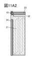
- FIG. 11A1 is a modified example of the configuration illustrated in FIG. 10B above. Here, a schematic top view of one subpixel is shown.
- FIG. 11A2 is a diagram in which only the outline of the conductive layer 32 in FIG. 11A1 is shown by a dashed line.
- the conductive layer 32 has two slits in the area overlapping with the semiconductor layer 21.
- the longitudinal direction of these slits is aligned with the extension direction of the conductive layer 24, and they are arranged side by side in the extension direction of the conductive layer 23.
- the longitudinal end of each slit is pointed at an angle.
- Each slit also has a shape that is symmetrical with respect to a 180 degree rotation. By using such a shape, the area required to arrange the slits can be reduced compared to using the V-shaped slits shown as an example in FIG. 10B. This makes it possible to realize a liquid crystal display device that combines high viewing angle characteristics with high definition.
- the aperture ratio can be extremely high at approximately 64.3%. Note that when a horizontal transistor with a top-gate structure is used, the aperture ratio is approximately 56.0% at the same resolution.
- FIG. 11B1 is a modified example of the configuration shown in FIG. 11A1.
- FIG. 11B2 shows only the outline of the conductive layer 32 in FIG. 11B2 by a dashed line.
- the conductive layer 32 has one slit.
- the slit has a rectangular shape with its longitudinal direction aligned with the extension direction of the conductive layer 24. By making the slit into this shape, extremely fine pixels can be formed.
- the wiring width of conductive layer 24 is narrower than the diameter of the opening that constitutes transistor 10. In this way, by thinning the wiring along the longitudinal direction of the subpixel, a high aperture ratio can be maintained even in a miniaturized pixel. On the other hand, it is preferable to make the wiring width of conductive layer 23, which is perpendicular to conductive layer 24, larger than the diameter of the opening, since this reduces the wiring resistance.
- the aperture ratio can be extremely high at approximately 52.3%. Note that when a horizontal transistor with a top-gate structure is used, the aperture ratio is approximately 41.1% at the same resolution.
- FIG. 12A is a modified example of the configuration illustrated in FIG. 11B1. Also, FIGS. 12B, 12C, 12D, and 12E respectively show only conductive layer 24, semiconductor layer 21, conductive layer 23, and conductive layer 32.
- the conductive layers 23 and 24 are thicker at the portions where the openings that form the transistors 10 are provided, and the other portions are narrower. This shape makes it possible to ensure a high aperture ratio even for extremely fine subpixels.
- part of the contour of the semiconductor layer 21 around the transistor 10 is curved (here, a circular arc).
- a pattern with a curved contour the degree of freedom in layout design is increased compared to when only straight lines are used, and patterns can be arranged at a higher density.
- a display device with a high aperture ratio can be realized even at high resolution.
- the aperture ratio of the subpixel illustrated in FIG. 12A is approximately 35.3%.
- a vertical transistor that can occupy an extremely small area is applied to a pixel of a liquid crystal display device, and a part of the semiconductor layer also serves as a pixel electrode, thereby realizing a liquid crystal display device that combines extremely high definition and a high aperture ratio.
- the vertical transistor of one embodiment of the present invention can have a smaller channel length and can pass a large current compared to a conventional horizontal transistor. Therefore, by applying such a transistor to a display device, a liquid crystal display device that can be driven at high speed and has high display quality can be realized.
- the vertical transistor of one embodiment of the present invention has an extremely small leakage current in an off state despite its small channel length, and therefore, by applying it to a liquid crystal display device, a potential written to a pixel can be held for a long time, thereby reducing power consumption by displaying at a low frame rate.
- This embodiment can be implemented by combining at least a portion of it with other embodiments described in this specification.
- the display device of this embodiment can be a high-resolution display device or a large display device. Therefore, the display device of this embodiment can be used in electronic devices with relatively large screens, such as television devices, desktop or notebook personal computers, computer monitors, digital signage, and large game machines such as pachinko machines, as well as in the display units of digital cameras, digital video cameras, digital photo frames, mobile phones, portable game machines, personal digital assistants, and audio playback devices.
- electronic devices with relatively large screens such as television devices, desktop or notebook personal computers, computer monitors, digital signage, and large game machines such as pachinko machines, as well as in the display units of digital cameras, digital video cameras, digital photo frames, mobile phones, portable game machines, personal digital assistants, and audio playback devices.
- the display device of this embodiment can be a high-definition display device. Therefore, the display device of this embodiment can be used, for example, in the display section of a wristwatch-type or bracelet-type information terminal (wearable device), as well as in the display section of a wearable device that can be worn on the head, such as a head-mounted display (HMD) or other VR device, or a glasses-type AR device.
- a wearable device such as a head-mounted display (HMD) or other VR device, or a glasses-type AR device.
- HMD head-mounted display
- AR device glasses-type AR device
- the semiconductor device of one embodiment of the present invention can be used in a display device or a module having the display device.
- the module having the display device include a module in which a connector such as a flexible printed circuit (hereinafter, referred to as FPC) or a TCP (Tape Carrier Package) is attached to the display device, and a module in which an integrated circuit (IC) is mounted by a COG (Chip On Glass) method or a COF (Chip On Film) method, etc.
- FPC flexible printed circuit
- TCP Tape Carrier Package
- FIG. 13 shows a perspective view of the display device 50A.
- Display device 50A has a configuration in which substrate 152 and substrate 151 are bonded together.
- substrate 152 is indicated by a dashed line.
- the display device 50A has a display unit 162, a connection unit 140, a circuit unit 164, wiring 165, etc.
- FIG. 13 shows an example in which an IC 173 and an FPC 172 are mounted on the display device 50A. Therefore, the configuration shown in FIG. 13 can also be said to be a display module having the display device 50A, an IC, and an FPC.
- connection portion 140 is provided on the outside of the display portion 162.
- the connection portion 140 can be provided along one side or multiple sides of the display portion 162. There may be one or multiple connection portions 140.
- FIG. 13 shows an example in which the connection portion 140 is provided so as to surround the four sides of the display portion 162.
- the connection portion 140 electrically connects the common electrode of the display element and the conductive layer, and can supply a potential to the common electrode. Note that if the connection portion 140 is not required, such as when the common electrode is provided on the substrate 151 side, it does not have to be provided.
- the circuit portion 164 has, for example, a scanning line driver circuit (also called a gate driver).
- the circuit portion 164 may also have both a scanning line driver circuit and a signal line driver circuit (also called a source driver).
- the wiring 165 has a function of supplying signals and power to the display unit 162 and the circuit unit 164.
- the signals and power are input to the wiring 165 from the outside via the FPC 172, or are input to the wiring 165 from the IC 173.
- FIG. 13 shows an example in which an IC 173 is provided on a substrate 151 by a COG method or a COF method.
- an IC having one or both of a scanning line driver circuit and a signal line driver circuit can be used as the IC 173.
- the display device 50A and the display module may be configured without an IC.
- the IC may be mounted on an FPC by a COF method or the like.
- the vertical transistor of one embodiment of the present invention can be applied to, for example, one or both of the display portion 162 and the circuit portion 164 of the display device 50A.
- the vertical transistor of one embodiment of the present invention can also be applied to the IC 173.
- the vertical transistor of one embodiment of the present invention can be provided on a silicon wafer. In this case, it is preferable to provide a transistor using single crystal silicon for its semiconductor layer and a vertical transistor of one embodiment of the present invention stacked above the transistor to form a circuit using two types of transistors.
- a vertical transistor of one embodiment of the present invention when a vertical transistor of one embodiment of the present invention is applied to a pixel circuit of a display device, the area occupied by the pixel circuit can be reduced compared to when a planar transistor is used, and a high-definition display device can be obtained.
- a vertical transistor of one embodiment of the present invention when a vertical transistor of one embodiment of the present invention is applied to a driver circuit of a display device (e.g., one or both of a gate line driver circuit and a source line driver circuit), the area occupied by the driver circuit can be reduced compared to when a planar transistor is used, and a display device with a narrow frame can be obtained.
- the vertical transistor of one embodiment of the present invention since the vertical transistor of one embodiment of the present invention has good electrical characteristics, the reliability of the display device can be improved by using it in the display device.
- the display unit 162 is an area in the display device 50A that displays an image, and has a number of periodically arranged pixels 210.
- Figure 13 shows an enlarged view of one pixel 210.
- pixel arrangements there are no particular limitations on the pixel arrangement in the display device of this embodiment, and various methods can be applied. Examples of pixel arrangements include a stripe arrangement, an S-stripe arrangement, a matrix arrangement, a delta arrangement, a Bayer arrangement, and a pentile arrangement.
- the pixel 210 shown in FIG. 13 has a subpixel 210R that emits red light, a subpixel 210G that emits green light, and a subpixel 210B that emits blue light.
- Each of the subpixels 210R, 210G, and 210B has a display element and a circuit that controls the driving of the display element.
- the display element for example, a liquid crystal element can be used.
- the device to be, for example, a transmissive liquid crystal display device, a reflective liquid crystal display device, or a semi-transmissive liquid crystal display device.
- various elements e.g., light-emitting elements other than liquid crystal elements can be used as display elements.
- light-emitting elements include self-luminous light-emitting elements such as LEDs (Light Emitting Diodes), OLEDs (Organic LEDs), and semiconductor lasers. Examples of LEDs that can be used include mini LEDs and micro LEDs.
- a shutter type or optical interference type MEMS (Micro Electro Mechanical Systems) element a display element using a microcapsule type, an electrophoresis type, an electrowetting type, or an electronic liquid powder (registered trademark) type.
- a QLED (Quantum-dot LED) using a light source and color conversion technology using quantum dot material may be used.
- Figure 14 shows an example of a cross section of the display device 50A when a portion of the area including the FPC 172, a portion of the circuit section 164, a portion of the display section 162, a portion of the connection section 140, and a portion of the area including the end portion are each cut away.
- Figure 14 is a schematic cross-sectional view of a VA mode liquid crystal element.
- Substrate 151 and substrate 152 are bonded together by adhesive layer 141. Liquid crystal 112 is sealed in the area surrounded by substrate 151, substrate 152, and adhesive layer 141.
- Substrate 152 has polarizing plate 130a on its outer surface.
- Substrate 151 has polarizing plate 130b on its outer surface.
- a backlight can be provided outside polarizing plate 130a or outside polarizing plate 130b.
- the substrate 151 is provided with a semiconductor layer 231 that functions as a pixel electrode of the liquid crystal element 60, a transistor 201, a plurality of transistors 202, a connection portion 204, a wiring 206, a spacer 124, and the like.
- the transistor 201 is provided in the circuit portion 164, and the transistor 202 is provided in the subpixel.
- the substrate 152 is provided with a colored layer 131, a light-shielding layer 132, an insulating layer 123, a common electrode 113, etc.
- Insulating layers such as insulating layer 211, insulating layer 212, insulating layer 213, insulating layer 214, and insulating layer 215 are provided on substrate 151.
- Insulating layer 211, insulating layer 212, and insulating layer 213 function as interlayer insulating layers (or spacers).
- a part of insulating layer 214 functions as a gate insulating layer for transistor 201 or transistor 202.
- Insulating layer 215 functions as a protective layer for transistors 201 and 202.
- Transistor 201 and transistor 202 have a conductive layer 222, a semiconductor layer 231, a part of the insulating layer 214, and a conductive layer 221.
- the semiconductor layer 231 of transistor 202 functions as a part of the pixel electrode.
- the conductive layer 222 functions as one of the source electrode and the drain electrode, and a part of the semiconductor layer 231 functions as the other of the source electrode and the drain electrode.
- the conductive layer 221 functions as a gate electrode.
- transistor 201 has a conductive layer 225.
- the conductive layer 225 functions as the other of the source electrode and the drain electrode.
- transistors exemplified in embodiment 1 can be applied to transistor 201 and transistor 202, and a detailed description thereof can be referred to.
- transistor 10a which has both a source electrode and a drain electrode in addition to the semiconductor layer, to transistor 201.
- a conductive layer 223 is provided on and in contact with the conductive layer 222.
- the conductive layer 223 contains a conductive material having a higher conductivity than the conductive layer 222, and functions as an auxiliary wiring.
- a conductive oxide is used for the conductive layer 222, it may be difficult to use it as a wiring due to high resistance.
- the conductivity of the conductive layer 222 can be supplemented by providing a conductive layer 223 having a higher conductivity than the conductive layer 222.
- the conductive layer 223 is provided on the conductive layer 222 here, the conductive layer 223 may be provided below the conductive layer 222. Although not shown here, it is preferable to provide a similar conductive layer in contact with the conductive layer 225.
- the liquid crystal element 60 has a part of the semiconductor layer 231 that functions as a pixel electrode, a common electrode 113, and liquid crystal 112 sandwiched between them.
- a conductive layer 224 is provided on the substrate 151 and is located on the same plane as the conductive layer 222.
- the conductive layer 224 has a portion that overlaps with the semiconductor layer 231 via the insulating layers 211, 212, and 213.
- a storage capacitance is formed by the semiconductor layer 231, the conductive layer 224, and the insulating layer between them. Note that it is sufficient that there is one or more insulating layers between the semiconductor layer 231 and the conductive layer 224, and any one or two of the insulating layers 211, 212, and 213 may be removed by etching.
- FIG. 14 also shows cross sections of two subpixels as an example of the display unit 162.
- One subpixel has at least a transistor 202, a liquid crystal element 60, and a colored layer 131.
- a full-color display can be achieved by selectively forming the colored layer 131 and arranging subpixels that exhibit red, green, and blue colors.
- a pixel circuit (subpixel circuit) is configured by the transistor 202, a portion of the semiconductor layer 231 that functions as a pixel electrode, wiring, etc.
- transistor 201 in the circuit portion 164 and the transistor 202 in the display portion 162 have different structures, they may have the same structure.
- the multiple transistors in the circuit portion 164 may all have the same structure, or transistors with different structures may be used in combination.
- the insulating layer 215 that covers the transistors is preferably made of a material that is difficult for impurities such as water or hydrogen to diffuse into.
- the insulating layer 215 can function as a barrier film. With this configuration, it is possible to effectively prevent impurities from diffusing into the transistors from the outside, thereby realizing a highly reliable touch panel.
- an insulating layer 123 is provided to cover the colored layer 131 and the light-shielding layer 132.
- the insulating layer 123 may also function as a planarizing film.
- the insulating layer 123 can make the surface of the common electrode 113 roughly flat, thereby making the alignment state of the liquid crystal 112 uniform.
- an alignment film for controlling the alignment of the liquid crystal 112 may be provided on the surfaces of the semiconductor layer 231, the common electrode 113, the insulating layer 215, etc. that come into contact with the liquid crystal 112.
- a display device to which the liquid crystal element 60 is applied can be a transmissive liquid crystal display device.
- a backlight is disposed on the substrate 152 side
- light from the backlight polarized by the polarizing plate 130a passes through the substrate 152, the common electrode 113, the liquid crystal 112, the semiconductor layer 231, and the substrate 151 to reach the polarizing plate 130b.
- the orientation of the liquid crystal 112 can be controlled by the voltage applied between the semiconductor layer 231 and the common electrode 113, and the optical modulation of light can be controlled.
- the intensity of the light emitted through the polarizing plate 130b can be controlled.
- the colored layer 131 absorbs light other than a specific wavelength range of the incident light, so that the extracted light is, for example, red light.
- a linear polarizing plate may be used as polarizing plate 130b, but a circular polarizing plate may also be used.
- a circular polarizing plate for example, a linear polarizing plate and a quarter-wave retardation plate stacked together may be used.
- a circular polarizing plate for polarizing plate 130b it is possible to suppress reflection of external light.
- polarizer 130b When a circular polarizer is used as polarizer 130b, a circular polarizer may also be used for polarizer 130a, or a normal linear polarizer may be used.
- the desired contrast can be achieved by adjusting the cell gap, orientation, drive voltage, etc. of the liquid crystal element used in liquid crystal element 60 according to the type of polarizer used for polarizers 130a and 130b.
- the common electrode 113 is electrically connected to a conductive layer provided on the substrate 151 side at the connection portion 140 by a connector 243. This allows a potential or signal to be supplied to the common electrode 113 from an FPC or IC arranged on the substrate 151 side.
- conductive particles can be used.
- the conductive particles particles of organic resin or silica, etc., whose surfaces are coated with a metal material can be used.
- Nickel or gold is preferably used as the metal material because it can reduce the contact resistance. It is also preferable to use particles coated with two or more metal materials in layers, such as nickel further coated with gold. It is also preferable to use a material that undergoes elastic or plastic deformation as the connector 243. In this case, the conductive particles may be crushed in the vertical direction as shown in FIG. 14. This increases the contact area between the connector 243 and the conductive layer electrically connected to it, reducing the contact resistance and suppressing the occurrence of problems such as poor connection.
- the connectors 243 are preferably arranged so that they are covered by the adhesive layer 141.
- the connectors 243 may be dispersed in the adhesive layer 141 before it hardens.
- the connectors 243 can be similarly applied to any configuration in which the adhesive layer 141 is used in the periphery, such as a display device with a solid sealing structure or a hollow sealing structure.
- connection portion 204 is provided in a region near the end of the substrate 151.
- the wiring 206 is electrically connected to the FPC 172 via a connection layer 242.
- the wiring 206 has an example of a layered structure similar to that of the conductive layer 222 and the conductive layer 223.
- a conductive oxide for the conductive layer 225. This allows for good connection characteristics with the semiconductor layer 231. Furthermore, it is preferable that the electrode that connects to the connector 243 in the connection portion 140 and the electrode that connects to the connection layer 242 in the connection portion 204 are formed in the same process using the same conductive film as the conductive layer 225. This makes it possible to prevent contact failures caused by the exposed portions of the connection portion 140 and the connection portion 204 oxidizing to form an insulating coating, thereby allowing for the realization of a highly reliable display device.
- FIG. 15 is a schematic cross-sectional view in which an FFS mode liquid crystal element is applied.
- a common electrode 113 is provided on the insulating layer 213, and an insulating layer 216 is provided covering the common electrode 113.
- a part of the semiconductor layer 231 is provided on the insulating layer 216.
- a part of the semiconductor layer 231 has a comb-like shape or a shape with slits in a plan view.
- the common electrode 113 is disposed so as to overlap the semiconductor layer 231. In the area overlapping with the colored layer 131, there is a part on the common electrode 113 where the semiconductor layer 231 is not disposed.
- FIG. 16 shows an example in which the top-bottom relationship between the semiconductor layer 231 and the common electrode 113 is reversed.
- the common electrode 113 has a comb-like shape or a shape with slits in a plan view, and is provided on the semiconductor layer 231 via the insulating layers 214 and 215.
- the semiconductor layer 231 and the common electrode 113 are stacked with the insulating layer 216 interposed between them, forming a capacitance. This eliminates the need to form a separate capacitance element, and allows the aperture ratio of the pixel to be increased.
- a transmissive liquid crystal display device by using a conductive material that transmits visible light as the common electrode 113, a transmissive liquid crystal display device can be obtained.
- a conductive material that transmits visible light it is preferable to use a conductive material that transmits visible light as both the semiconductor layer 231 and the common electrode 113, since this can further increase the aperture ratio.
- a reflective layer that reflects visible light may be provided over the liquid crystal element 60.
- liquid crystals exhibiting a blue phase without using an alignment film may be used.
- the blue phase is one of the liquid crystal phases, and is the phase that appears just before the cholesteric phase transitions to the isotropic phase when the temperature of cholesteric liquid crystal is increased. Since the blue phase appears only in a narrow temperature range, a liquid crystal composition containing a few weight percent or more of a chiral agent is used in the liquid crystal layer to improve the temperature range.
- a liquid crystal composition containing a liquid crystal exhibiting a blue phase and a chiral agent has a short response speed and is optically isotropic.
- a liquid crystal composition containing a liquid crystal exhibiting a blue phase and a chiral agent does not require an alignment process and has a small viewing angle dependency.
- a rubbing process is also not required, so electrostatic damage caused by the rubbing process can be prevented, and defects and damage to the liquid crystal display device during the manufacturing process can be reduced.
- [Cross-sectional configuration example 3] 17 shows an example in which a liquid crystal element to which an IPS mode is applied is used as the liquid crystal element 60.
- the liquid crystal element 60 has a part of a semiconductor layer 231, a liquid crystal 112, and a common electrode 113.
- a portion of the semiconductor layer 231 and the common electrode 113 are provided on the insulating layer 213.
- the portion of the semiconductor layer 231 and the common electrode 113 each have a comb-like shape in a plan view, and are arranged so as to interdigitate with each other.
- the semiconductor layer 231 and the common electrode 113 are preferably formed by processing the same conductive film. Note that in FIG. 17, the semiconductor layer 231 and the common electrode 113 are given different hatching patterns for ease of explanation.
- This embodiment can be implemented by combining at least a portion of it with other embodiments described in this specification.
- the display device shown in FIG. 18A has a pixel portion 502, a driver circuit portion 504, a protection circuit 506, and a terminal portion 507. Note that the protection circuit 506 may not be provided.
- a transistor according to one embodiment of the present invention can be applied to one or both of the pixel portion 502 and the driver circuit portion 504.
- a transistor according to one embodiment of the present invention can also be applied to the protection circuit 506.
- the pixel section 502 has a plurality of pixel circuits 501 arranged in X rows and Y columns (X and Y are each independently a natural number of 2 or more).
- Each pixel circuit 501 has a circuit that drives a display element.
- the driver circuit unit 504 has driver circuits such as a gate driver 504a that outputs scanning signals to the gate lines GL_1 to GL_X, and a source driver 504b that supplies data signals to the data lines DL_1 to DL_Y.
- the gate driver 504a may have at least a shift register.
- the source driver 504b may be configured using a shift register, a digital-to-analog conversion circuit, a latch circuit, etc.
- the terminal section 507 is a section that has terminals for inputting power, control signals, image signals, etc. from an external circuit to the display device.
- the protection circuit 506 is a circuit that connects a wiring to which it is connected to another wiring when a potential outside a certain range is applied to the wiring.
- the protection circuit 506 shown in FIG. 18A is connected to various wirings such as a gate line GL and a data line DL. Note that in FIG. 18A, the protection circuit 506 is shown with a hatched pattern to distinguish it from the pixel circuit 501.
- the gate driver 504a and the source driver 504b may be provided on the same substrate as the pixel section 502, or an IC on which a gate driver circuit or a source driver circuit is separately formed may be mounted on the substrate on which the pixel section 502 is provided using a COG (chip on glass) method or the like.
- an FPC flexible printed circuit
- ACF anisotropic conductive film
- the pixel portion 502 and the gate driver 504a are preferably manufactured over the same substrate and through the same process. At this time, it is preferable to provide a transistor of one embodiment of the present invention in each of the pixel portion 502 and the gate driver 504a. Furthermore, when an IC is used for the source driver 504b, it is preferable to provide a demultiplexer circuit over the substrate because the number of terminals of the IC can be reduced. At this time, it is preferable to apply a transistor of one embodiment of the present invention to the demultiplexer circuit.
- FIG. 18B shows an example of a pixel circuit configuration that can be applied to pixel circuit 501.
- the pixel circuit 501 shown in FIG. 18B includes a liquid crystal element 570, a transistor 550, and a capacitor element 560.
- the pixel circuit 501 is also connected to a data line DL_n, a gate line GL_m, a potential supply line VL, and the like.
- a vertical transistor according to one embodiment of the present invention can be used as transistor 550.
- the potential of one of the pair of electrodes of the liquid crystal element 570 is set appropriately according to the specifications of the pixel circuit 501.
- the orientation state of the liquid crystal element 570 is set by the data written thereto.
- a common potential (common potential) may be applied to one of the pair of electrodes of the liquid crystal element 570 in each of the multiple pixel circuits 501.
- a different potential may be applied to one of the pair of electrodes of the liquid crystal element 570 in the pixel circuit 501 in each row.
- the pixel circuit 501 shown in FIG. 18C includes a transistor 552, a transistor 554, a capacitor 562, and a light-emitting element 572.
- the pixel circuit 501 is connected to a data line DL_n, a gate line GL_m, a potential supply line VL_a, a potential supply line VL_b, and the like.
- a high power supply potential VDD is applied to one of the potential supply lines VL_a and VL_b, and a low power supply potential VSS is applied to the other.
- the current flowing through the light-emitting element 572 is controlled according to the potential applied to the gate of the transistor 554, thereby controlling the light emission brightness from the light-emitting element 572.
- FIG. 19A shows a circuit diagram of a pixel circuit 400.
- the pixel circuit 400 includes a transistor M1, a transistor M2, a capacitor C1, and a circuit 401.
- the pixel circuit 400 is also connected to wiring S1, wiring S2, wiring G1, and wiring G2.
- Transistor M1 and transistor M2 can be vertical transistors according to one embodiment of the present invention.
- the gate of the transistor M1 is connected to the wiring G1, one of the source and drain is connected to the wiring S1, and the other is connected to one electrode of the capacitor C1.
- the gate of the transistor M2 is connected to the wiring G2, one of the source and drain is connected to the wiring S2, and the other is connected to the other electrode of the capacitor C1 and the circuit 401.
- Circuit 401 is a circuit that includes at least one display element.
- the display element is a liquid crystal element.
- the node connecting transistor M1 and capacitor C1 is node N1
- the node connecting transistor M2 and circuit 401 is node N2.
- the pixel circuit 400 can maintain the potential of node N1 by turning off transistor M1. Also, the pixel circuit 400 can maintain the potential of node N2 by turning off transistor M2. Also, by writing a predetermined potential to node N1 via transistor M1 while transistor M2 is turned off, the potential of node N2 can be changed according to the change in the potential of node N1 due to capacitive coupling via capacitor C1.
- the transistor using an oxide semiconductor as exemplified in embodiment 1 can be used as one or both of transistor M1 and transistor M2. Therefore, the potential of node N1 or node N2 can be held for a long period of time due to an extremely low off-current. Note that when the period for holding the potential of each node is short (specifically, when the frame frequency is 30 Hz or more), a transistor using a semiconductor such as silicon may be used.
- Fig. 19B is a timing chart relating to the operation of the pixel circuit 400. Note that, in order to simplify the description, the influence of various resistances such as wiring resistance, parasitic capacitance, and threshold voltage of a transistor is not taken into consideration here.
- Period T1 is a period in which a potential is written to node N2
- period T2 is a period in which a potential is written to node N1.
- Period T1 In the period T1, a potential that turns on the transistor is applied to both the wiring G1 and the wiring G2. A fixed potential Vref is supplied to the wiring S1, and a first data potential Vw is supplied to the wiring S2.
- the node N1 is supplied with a potential Vref from the wiring S1 through the transistor M1.
- the node N2 is supplied with a first data potential Vw from the wiring S2 through the transistor M2. Therefore, the potential difference Vw - Vref is held in the capacitor C1.
- Period T2 In the next period T2, a potential that turns on the transistor M1 is applied to the wiring G1, and a potential that turns off the transistor M2 is applied to the wiring G2.
- a second data potential Vdata is supplied to the wiring S1.
- a predetermined constant potential is applied to the wiring S2, or the wiring S2 may be in a floating state.
- the second data potential Vdata is applied to the node N1 from the wiring S1 through the transistor M1.
- the potential of the node N2 changes by a potential dV in response to the second data potential Vdata due to capacitive coupling by the capacitor C1. That is, a potential obtained by adding the first data potential Vw and the potential dV is input to the circuit 401.
- the potential dV is shown to be a positive value in FIG. 19B, it may be a negative value. That is, the second data potential Vdata may be lower than the potential Vref .
- the potential dV is roughly determined by the capacitance value of the capacitor C1 and the capacitance value of the circuit 401.
- the potential dV becomes close to the second data potential Vdata .
- the pixel circuit 400 can combine two types of data signals to generate a potential to be supplied to the circuit 401 including the display element, making it possible to perform gradation correction within the pixel circuit 400.
- the pixel circuit 400 can also generate a potential that exceeds the maximum potential that can be supplied by the source driver connected to the wiring S1 and wiring S2. For example, when a light-emitting element is used, a high dynamic range (HDR) display can be performed. When a liquid crystal element is used, overdrive driving can be realized.
- HDR high dynamic range
- Example using liquid crystal element 19C includes a circuit 401LC.
- the circuit 401LC includes a liquid crystal element LC and a capacitor C2.
- One electrode of the liquid crystal element LC is connected to the node N2 and one electrode of the capacitor C2, and the other electrode is connected to a wiring to which a potential V com2 is applied.
- the other electrode of the capacitor C2 is connected to a wiring to which a potential V com1 is applied.
- Capacitor C2 functions as a storage capacitor. Note that capacitor C2 can be omitted if not required.
- the pixel circuit 400LC can supply a high voltage to the liquid crystal element LC, which makes it possible to, for example, realize high-speed display by overdriving, and to apply liquid crystal materials with high driving voltages.
- a correction signal to the wiring S1 or wiring S2, it is possible to correct the gradation according to the operating temperature, the deterioration state of the liquid crystal element LC, etc.
- Example using light-emitting element 19D includes a circuit 401EL.
- the circuit 401EL includes a light-emitting element EL, a transistor M3, and a capacitor C2.
- the transistor M3 has a gate connected to the node N2 and one electrode of the capacitor C2, a source and a drain connected to a wiring to which a potential VH is applied, and the other connected to one electrode of the light-emitting element EL.
- the other electrode of the capacitor C2 is connected to a wiring to which a potential Vcom is applied.
- the other electrode of the light-emitting element EL is connected to a wiring to which a potential VL is applied.
- Transistor M3 has the function of controlling the current supplied to the light-emitting element EL.
- Capacitor C2 functions as a storage capacitor. Capacitor C2 can be omitted if not required.
- the anode side of the light-emitting element EL is connected to the transistor M3, but the cathode side of the light-emitting element EL may be connected to the transistor M3.
- the values of the potentials VH and VL can be changed as appropriate.
- the pixel circuit 400EL can achieve, for example, HDR display by applying a high potential to the gate of the transistor M3 to pass a large current through the light-emitting element EL.
- a correction signal to the wiring S1 or wiring S2, it is also possible to correct variations in the electrical characteristics of the transistor M3, the light-emitting element EL, etc.
- circuit is not limited to the examples shown in Figures 19C and 19D, and may include additional transistors, capacitance, etc.
- This embodiment can be implemented by combining at least a portion of it with other embodiments described in this specification.
- FIG. 20 shows a block diagram of the touch panel module 6500.
- the touch panel module 6500 has a touch panel 6510 and an IC 6520.
- the touch panel 6510 has a display portion 6511, an input portion 6512, a scanning line driver circuit 6513, a sensor driver circuit 6503, and a detection circuit 6504.
- the display portion 6511 has a plurality of pixels, a plurality of signal lines, and a plurality of scanning lines, and has a function of displaying an image.
- the input portion 6512 has a plurality of sensor elements that detect contact or proximity of a detectable object to the touch panel 6510, and has a function as a touch sensor.
- the scanning line driver circuit 6513 has a function of outputting a scanning signal to the scanning line of the display portion 6511.
- the sensor driving circuit 6503 has a function of outputting a signal that drives the sensor element of the input unit 6512.
- the sensor driving circuit 6503 can be configured by combining a shift register circuit and a buffer circuit.
- the detection circuit 6504 has the function of amplifying the output signal from the sensor element of the input unit 6512 and outputting it to the AD conversion circuit 6507.
- the touch panel 6510 is shown here as being composed of a separate display section 6511 and input section 6512, but it may be a so-called in-cell type touch panel that has both the function of displaying images and the function of acting as a touch sensor.
- a capacitance type can be applied as a touch sensor type that can be used as the input unit 6512.
- capacitance types include a surface capacitance type and a projected capacitance type.
- projected capacitance types include a self-capacitance type and a mutual capacitance type. The mutual capacitance type is preferable because it allows simultaneous multi-point detection.
- various types of sensors that can detect the approach, contact, or pressure of a detectable object such as a finger or stylus can also be applied to the input unit 6512.
- various types of sensors can be used, such as a resistive film type, a surface acoustic wave type, an infrared type, and an optical type.
- Typical in-cell touch panels include hybrid in-cell and full in-cell.
- the hybrid in-cell type refers to a configuration in which electrodes constituting a touch sensor are provided on both the substrate supporting the display element and the opposing substrate, or on the opposing substrate.
- the full in-cell type refers to a configuration in which electrodes constituting a touch sensor are provided on the substrate supporting the display element.
- a full in-cell touch panel is preferable because it simplifies the configuration of the opposing substrate.
- a full in-cell type in which the electrodes constituting the display element also serve as the electrodes constituting the touch sensor is preferable because it simplifies the manufacturing process and reduces manufacturing costs.
- the display unit 6511 preferably has an extremely high resolution such as HD (1280 x 720 pixels), FHD (1920 x 1080 pixels), WQHD (2560 x 1440 pixels), WQXGA (2560 x 1600 pixels), 4K (3840 x 2160 pixels), or 8K (7680 x 4320 pixels). In particular, a resolution of 4K, 8K, or higher is preferable.
- the pixel density (resolution) of the pixels provided in the display unit 6511 is preferably 300 ppi or more, preferably 500 ppi or more, more preferably 800 ppi or more, more preferably 1000 ppi or more, and more preferably 1200 ppi or more.
- the display unit 6511 having such high resolution and high resolution makes it possible to enhance the sense of realism and depth.
- the IC 6520 has a circuit unit 6501, a signal line driver circuit 6502, and an AD conversion circuit 6507.
- the circuit unit 6501 has a timing controller 6505, an image processing circuit 6506, etc.
- the signal line driver circuit 6502 has a function of outputting an analog image signal (also called a video signal) to a signal line of the display portion 6511.
- the signal line driver circuit 6502 can have a configuration in which a shift register, a digital-analog converter circuit (DAC), a latch circuit, a buffer circuit, and the like are combined.
- the touch panel 6510 may also have a demultiplexer circuit connected to the signal line.
- the AD conversion circuit 6507 has a function of converting an analog signal input from the detection circuit 6504 into a digital signal and outputting it to the circuit unit 6501.
- the AD conversion circuit 6507 can have a configuration including an amplifier circuit in addition to an analog-digital conversion circuit (ADC: Analog-Digital Converter).
- the image processing circuit 6506 of the circuit unit 6501 has a function of generating and outputting a signal that drives the display unit 6511 of the touch panel 6510, a function of generating and outputting a signal that drives the input unit 6512, and a function of analyzing the signal output from the input unit 6512 and outputting it to the CPU 6540.
- the image processing circuit 6506 has a function of generating a video signal according to an instruction from the CPU 6540.
- the image processing circuit 6506 also has a function of performing signal processing on the video signal in accordance with the specifications of the display unit 6511, converting it into an analog video signal, and supplying it to the signal line driving circuit 6502.
- the image processing circuit 6506 also has a function of generating a driving signal to be output to the sensor driving circuit 6503 according to an instruction from the CPU 6540.
- the image processing circuit 6506 also has a function of analyzing a signal input from the detection circuit 6504 via the AD conversion circuit 6507, and outputting it to the CPU 6540 as position information.
- the timing controller 6505 has a function of generating and outputting signals (signals such as a clock signal and a start pulse signal) to be output to the scanning line driving circuit 6513 and the sensor driving circuit 6503 based on a synchronization signal included in the video signal processed by the image processing circuit 6506.
- the timing controller 6505 may also have a function of generating and outputting a signal that specifies the timing at which the detection circuit 6504 outputs a signal.
- the timing controller 6505 outputs a signal that is synchronized with the signal to be output to the scanning line driving circuit 6513 and the signal to be output to the sensor driving circuit 6503.
- the touch panel 6510 can be driven by dividing one frame period into a period in which pixel data is rewritten and a period in which sensing is performed.
- the detection sensitivity and detection accuracy can be improved.
- the image processing circuit 6506 can be configured to have a processor, for example.
- a microprocessor such as a DSP (Digital Signal Processor) or a GPU (Graphics Processing Unit) can be used.
- These microprocessors may also be configured to be realized by a PLD (Programmable Logic Device) such as an FPGA (Field Programmable Gate Array) or an FPAA (Field Programmable Analog Array).
- the image processing circuit 6506 performs various data processing, program control, etc. by interpreting and executing commands from various programs using the processor. Programs that can be executed by the processor may be stored in a memory area of the processor, or may be stored in a separately provided storage device.
- the transistor that uses an oxide semiconductor in a channel formation region and has an extremely low off-current in at least one of the display portion 6511, the input portion 6512, the scanning line driver circuit 6513, the sensor driver circuit 6503, and the detection circuit 6504 of the touch panel 6510. Since the off-current of the transistor is extremely low, the data retention period can be secured for a long period by using the transistor as a switch for retaining charge (data) flowing into a capacitor that functions as a memory element.
- the transistor may be applied to the circuit unit 6501, the signal line driver circuit 6502, the AD conversion circuit 6507, the CPU 6540 provided externally, or the like, which are included in the IC 6520.
- the image processing circuit 6506 operates only when necessary, and in other cases, the information of the immediately preceding processing is saved in the storage element, thereby enabling so-called normally-off computing, in which the power supply to the image processing circuit 6506 is cut off when not in use, thereby enabling low power consumption of the touch panel module 6500 and the electronic device in which it is implemented.
- the circuit unit 6501 has a configuration including a timing controller 6505 and an image processing circuit 6506, but the image processing circuit 6506 itself, or a circuit having some of the functions of the image processing circuit 6506, may be provided outside the IC 6520. Alternatively, the functions of the image processing circuit 6506, or some of the functions, may be performed by the CPU 6540.
- the circuit unit 6501 may have a configuration including a signal line driver circuit 6502, a timing controller 6505, and an AD conversion circuit 6507.
- the circuit unit 6501 may not be included in the IC 6520.
- the IC 6520 may have a signal line driver circuit 6502 and an AD conversion circuit 6507.
- an IC including the circuit unit 6501 may be provided separately, and multiple ICs 6520 that do not have the circuit unit 6501 may be arranged, or the IC 6520 may be combined with an IC that only has the signal line driver circuit 6502.
- 21A, 21B, and 21C are schematic diagrams of a touch panel module 6500 incorporating an IC 6520.
- the touch panel module 6500 shown in FIG. 21A includes a substrate 6531, an opposing substrate 6532, multiple FPCs 6533, an IC 6520, an IC 6530, etc. Also, between the substrate 6531 and the opposing substrate 6532, there are a display section 6511, an input section 6512, a scanning line driving circuit 6513, a sensor driving circuit 6503, and a detection circuit 6504.
- the IC 6520 and the IC 6530 are mounted on the substrate 6531 by a mounting method such as the COG (Chip On Glass) method.
- the IC6530 is an IC similar to the IC6520 described above, which has only the signal line driver circuit 6502, or has the signal line driver circuit 6502 and a circuit unit 6501. Signals are supplied to the IC6520 and IC6530 from the outside via the FPC6533. Also, signals can be output from the IC6520 or IC6530 to the outside via the FPC6533.
- FIG. 21A shows an example of a configuration in which two scanning line driver circuits 6513 are provided to sandwich the display portion 6511. Also, a configuration having an IC 6530 in addition to an IC 6520 is shown. This type of configuration can be suitably used when the display portion 6511 has extremely high resolution.
- FIG. 21B shows an example where one IC 6520 and one FPC 6533 are mounted. In this way, by consolidating the functions into one IC 6520, the number of parts can be reduced, which is preferable. Also, FIG. 21B shows an example where the scanning line driver circuit 6513 is arranged along one of the two short sides of the display portion 6511 that is closer to the FPC 6533.
- FIG. 21C shows an example of a configuration having a PCB (Printed Circuit Board) 6534 on which an image processing circuit 6506 and the like are mounted.
- ICs 6520 and 6530 on a substrate 6531 are electrically connected to PCB 6534 by an FPC 6533.
- FPC 6533 a configuration that does not have the image processing circuit 6506 described above can be applied to IC 6520.
- IC6520 and IC6530 may be mounted on FPC6533 instead of substrate 6531.
- IC6520 and IC6530 may be mounted on FPC6533 by a mounting method such as COF or TAB.
- a configuration in which the FPC 6533, IC 6520 (and IC 6530), etc. are arranged on the short side of the display section 6511 allows for a narrow frame, and is therefore suitable for use in electronic devices such as smartphones, mobile phones, and tablet terminals.
- a configuration using a PCB 6534 as shown in Figure 21C can be suitable for use in television devices, monitor devices, tablet terminals, and notebook personal computers, for example.
- This embodiment can be implemented by combining at least a portion of it with other embodiments described in this specification.
- the electronic device of this embodiment has a display device of one embodiment of the present invention in a display portion.
- the display device of one embodiment of the present invention can easily achieve high definition and high resolution. Therefore, it can be used in the display portion of various electronic devices.
- the semiconductor device of one embodiment of the present invention can also be applied to portions other than the display portion of electronic devices.
- portions other than the display portion of electronic devices For example, by using the semiconductor device of one embodiment of the present invention in a control portion of an electronic device, it is possible to reduce power consumption, which is preferable.
- Electronic devices include, for example, electronic devices with relatively large screens such as television sets, desktop or notebook personal computers, computer monitors, digital signage, large game machines such as pachinko machines, as well as digital cameras, digital video cameras, digital photo frames, mobile phones, portable game machines, personal digital assistants, and audio playback devices.
- the display device of one embodiment of the present invention can be used in electronic devices having a relatively small display area because it is possible to increase the resolution.
- electronic devices include wristwatch-type and bracelet-type information terminals (wearable devices), as well as wearable devices that can be worn on the head, such as VR devices such as head-mounted displays, glasses-type AR devices, and MR devices.
- the electronic device of this embodiment may have a sensor (including the function of sensing, detecting, or measuring force, displacement, position, velocity, acceleration, angular velocity, rotation speed, distance, light, liquid, magnetism, temperature, chemicals, sound, time, hardness, electric field, current, voltage, power, radiation, flow rate, humidity, gradient, vibration, odor, or infrared light).
- a sensor including the function of sensing, detecting, or measuring force, displacement, position, velocity, acceleration, angular velocity, rotation speed, distance, light, liquid, magnetism, temperature, chemicals, sound, time, hardness, electric field, current, voltage, power, radiation, flow rate, humidity, gradient, vibration, odor, or infrared light).
- the electronic device of this embodiment can have various functions. For example, it can have a function to display various information (still images, videos, text images, etc.) on the display unit, a touch panel function, a function to display a calendar, date or time, etc., a function to execute various software (programs), a wireless communication function, a function to read out programs or data recorded on a recording medium, etc.
- a function to display various information still images, videos, text images, etc.
- a touch panel function a function to display a calendar, date or time, etc.
- a function to execute various software (programs) a wireless communication function
- a function to read out programs or data recorded on a recording medium etc.
- the electronic device 7000 shown in FIG. 22A is a portable information terminal that can be used as a smartphone.
- the electronic device 7000 includes a housing 7001, a display unit 7002, a power button 7003, a button 7004, a speaker 7005, a microphone 7006, a camera 7007, and a light source 7008.
- the display unit 7002 has a touch panel function.
- a display device can be applied to the display portion 7002.
- FIG. 22B is a schematic cross-sectional view including the end of the housing 7001 on the microphone 7006 side.
- a translucent protective member 7010 is provided on the display surface side of the housing 7001, and a display panel 7011, optical members 7012, a touch sensor panel 7013, a printed circuit board 7017, a battery 7018, etc. are arranged in the space surrounded by the housing 7001 and the protective member 7010.
- the display panel 7011, the optical member 7012, and the touch sensor panel 7013 are fixed to the protective member 7010 by an adhesive layer (not shown).
- a part of the display panel 7011 is folded back in the area outside the display unit 7002, and an FPC 7015 is connected to the folded back part.
- An IC 7016 is mounted on the FPC 7015.
- the FPC 7015 is connected to a terminal provided on a printed circuit board 7017.
- the display device according to one embodiment of the present invention can be applied to the display panel 7011. Therefore, an extremely lightweight electronic device can be realized.
- the display panel 7011 is extremely thin, a large-capacity battery 7018 can be mounted thereon while keeping the thickness of the electronic device small.
- a connection portion with the FPC 7015 on the back side of the pixel portion, an electronic device with a narrow frame can be realized.
- FIG. 22C shows an example of a television device.
- a display unit 7002 is built into a housing 7101.
- the housing 7101 is supported by a stand 7103.
- a display device can be applied to the display portion 7002.
- the television set 7100 shown in FIG. 22C can be operated using operation switches provided on the housing 7101 and a separate remote control 7111.
- the display portion 7002 may be provided with a touch sensor, and the television set 7100 may be operated by touching the display portion 7002 with a finger or the like.
- the remote control 7111 may have a display portion that displays information output from the remote control 7111.
- the channel and volume can be operated using operation keys or a touch panel provided on the remote control 7111, and the image displayed on the display portion 7002 can be operated.
- the television device 7100 is configured to include a receiver and a modem.
- the receiver can receive general television broadcasts.
- by connecting to a wired or wireless communication network via the modem it is also possible to carry out one-way (from sender to receiver) or two-way (between sender and receiver, or between receivers, etc.) information communication.
- FIG. 22D shows an example of a notebook personal computer.
- the notebook personal computer 7200 has a housing 7211, a keyboard 7212, a pointing device 7213, an external connection port 7214, and the like.
- a display unit 7002 is built into the housing 7211.
- a display device can be applied to the display portion 7002.
- Figures 22E and 22F show an example of digital signage.
- the digital signage 7300 shown in FIG. 22E has a housing 7301, a display unit 7002, and a speaker 7303. It can also have LED lamps, operation keys (including a power switch or an operation switch), connection terminals, various sensors, a microphone, etc.
- FIG. 22F shows digital signage 7400 attached to a cylindrical pole 7401.
- Digital signage 7400 has a display unit 7002 that is provided along the curved surface of pole 7401.
- a display device of one embodiment of the present invention can be applied to the display portion 7002.
- a touch panel By applying a touch panel to the display unit 7002, not only can images or videos be displayed on the display unit 7002, but the user can also intuitively operate it, which is preferable. Furthermore, when used to provide information such as route information or traffic information, the intuitive operation can improve usability.
- the digital signage 7300 or the digital signage 7400 can be linked via wireless communication with an information terminal 7311 or an information terminal 7411 such as a smartphone carried by a user.
- advertising information displayed on the display unit 7002 can be displayed on the screen of the information terminal 7311 or the information terminal 7411.
- the display on the display unit 7002 can be switched by operating the information terminal 7311 or the information terminal 7411.
- the digital signage 7300 or the digital signage 7400 can also be made to run a game using the screen of the information terminal 7311 or the information terminal 7411 as an operating means (controller). This allows an unspecified number of users to participate in and enjoy the game at the same time.
- This embodiment can be implemented by combining at least a portion of it with other embodiments described in this specification.
- 10a transistor, 10: transistor, 11: substrate, 12: substrate, 20: opening, 21: semiconductor layer, 22: insulating layer, 23: conductive layer, 24: conductive layer, 25: insulating layer, 26: conductive layer, 28: insulating layer, 29a: insulating layer, 29b: insulating layer, 30: liquid crystal element, 31: conductive layer, 32: conductive layer, 33: liquid crystal, 34: insulating layer, 35: conductive layer, 41: alignment film, 42: alignment film, 43: colored layer, 44: light shielding layer, 45: insulating layer, 46: insulating layer
Landscapes
- Physics & Mathematics (AREA)
- Engineering & Computer Science (AREA)
- Nonlinear Science (AREA)
- General Physics & Mathematics (AREA)
- Microelectronics & Electronic Packaging (AREA)
- Mathematical Physics (AREA)
- Chemical & Material Sciences (AREA)
- Crystallography & Structural Chemistry (AREA)
- Optics & Photonics (AREA)
- Theoretical Computer Science (AREA)
- Thin Film Transistor (AREA)
Priority Applications (1)
| Application Number | Priority Date | Filing Date | Title |
|---|---|---|---|
| JP2025520196A JPWO2024236433A1 (https=) | 2023-05-17 | 2024-05-10 |
Applications Claiming Priority (2)
| Application Number | Priority Date | Filing Date | Title |
|---|---|---|---|
| JP2023-081483 | 2023-05-17 | ||
| JP2023081483 | 2023-05-17 |
Publications (1)
| Publication Number | Publication Date |
|---|---|
| WO2024236433A1 true WO2024236433A1 (ja) | 2024-11-21 |
Family
ID=93519035
Family Applications (1)
| Application Number | Title | Priority Date | Filing Date |
|---|---|---|---|
| PCT/IB2024/054541 Ceased WO2024236433A1 (ja) | 2023-05-17 | 2024-05-10 | 表示装置 |
Country Status (2)
| Country | Link |
|---|---|
| JP (1) | JPWO2024236433A1 (https=) |
| WO (1) | WO2024236433A1 (https=) |
Citations (4)
| Publication number | Priority date | Publication date | Assignee | Title |
|---|---|---|---|---|
| JP2008009425A (ja) * | 2006-06-02 | 2008-01-17 | Semiconductor Energy Lab Co Ltd | 液晶表示装置及び電子機器 |
| JP2016001292A (ja) * | 2013-09-13 | 2016-01-07 | 株式会社半導体エネルギー研究所 | 表示装置 |
| JP2017168761A (ja) * | 2016-03-18 | 2017-09-21 | 株式会社ジャパンディスプレイ | 半導体装置 |
| US20200312937A1 (en) * | 2019-03-25 | 2020-10-01 | Samsung Display Co., Ltd. | Thin film transistor substrate, display apparatus and method of manufacturing the same |
-
2024
- 2024-05-10 JP JP2025520196A patent/JPWO2024236433A1/ja active Pending
- 2024-05-10 WO PCT/IB2024/054541 patent/WO2024236433A1/ja not_active Ceased
Patent Citations (4)
| Publication number | Priority date | Publication date | Assignee | Title |
|---|---|---|---|---|
| JP2008009425A (ja) * | 2006-06-02 | 2008-01-17 | Semiconductor Energy Lab Co Ltd | 液晶表示装置及び電子機器 |
| JP2016001292A (ja) * | 2013-09-13 | 2016-01-07 | 株式会社半導体エネルギー研究所 | 表示装置 |
| JP2017168761A (ja) * | 2016-03-18 | 2017-09-21 | 株式会社ジャパンディスプレイ | 半導体装置 |
| US20200312937A1 (en) * | 2019-03-25 | 2020-10-01 | Samsung Display Co., Ltd. | Thin film transistor substrate, display apparatus and method of manufacturing the same |
Also Published As
| Publication number | Publication date |
|---|---|
| JPWO2024236433A1 (https=) | 2024-11-21 |
Similar Documents
| Publication | Publication Date | Title |
|---|---|---|
| US11835810B2 (en) | Display device | |
| JP7622275B2 (ja) | 表示装置及び発光装置 | |
| KR102643613B1 (ko) | 표시 장치, 표시 모듈, 및 전자 기기 | |
| JP2025016495A (ja) | 半導体装置 | |
| US20190362683A1 (en) | Display device and electronic device | |
| TW201826353A (zh) | 顯示裝置、顯示模組及電子裝置 | |
| JP2018072822A (ja) | 表示装置およびその動作方法 | |
| JP2022126638A (ja) | 表示装置及び複合酸化物半導体 | |
| JP2024019128A (ja) | 表示装置 | |
| JP2018120214A (ja) | 表示装置 | |
| CN107735725B (zh) | 液晶显示装置及电子设备 | |
| TWI713004B (zh) | 顯示裝置、顯示模組及電子裝置 | |
| WO2024236433A1 (ja) | 表示装置 | |
| WO2024241133A1 (ja) | 半導体装置、表示装置、表示モジュール、電子機器 | |
| WO2024252247A1 (ja) | 表示装置、表示モジュール、電子機器 | |
| WO2025032416A1 (ja) | 半導体装置、表示装置、及び半導体装置の作製方法 | |
| WO2025125998A1 (ja) | 半導体装置、および表示装置 | |
| WO2024228089A1 (ja) | 表示モジュール、電子機器 | |
| WO2026093872A1 (ja) | 半導体装置 |
Legal Events
| Date | Code | Title | Description |
|---|---|---|---|
| 121 | Ep: the epo has been informed by wipo that ep was designated in this application |
Ref document number: 24806741 Country of ref document: EP Kind code of ref document: A1 |
|
| WWE | Wipo information: entry into national phase |
Ref document number: 2025520196 Country of ref document: JP |
|
| NENP | Non-entry into the national phase |
Ref country code: DE |