WO2024225142A1 - 電磁波反射構造体 - Google Patents
電磁波反射構造体 Download PDFInfo
- Publication number
- WO2024225142A1 WO2024225142A1 PCT/JP2024/015320 JP2024015320W WO2024225142A1 WO 2024225142 A1 WO2024225142 A1 WO 2024225142A1 JP 2024015320 W JP2024015320 W JP 2024015320W WO 2024225142 A1 WO2024225142 A1 WO 2024225142A1
- Authority
- WO
- WIPO (PCT)
- Prior art keywords
- electromagnetic wave
- conductive parts
- wave reflecting
- reflecting structure
- conductive
- Prior art date
- Legal status (The legal status is an assumption and is not a legal conclusion. Google has not performed a legal analysis and makes no representation as to the accuracy of the status listed.)
- Ceased
Links
Images



Classifications
-
- H—ELECTRICITY
- H01—ELECTRIC ELEMENTS
- H01Q—ANTENNAS, i.e. RADIO AERIALS
- H01Q15/00—Devices for reflection, refraction, diffraction or polarisation of waves radiated from an antenna, e.g. quasi-optical devices
- H01Q15/14—Reflecting surfaces; Equivalent structures
-
- H—ELECTRICITY
- H01—ELECTRIC ELEMENTS
- H01Q—ANTENNAS, i.e. RADIO AERIALS
- H01Q17/00—Devices for absorbing waves radiated from an antenna; Combinations of such devices with active antenna elements or systems
-
- H—ELECTRICITY
- H05—ELECTRIC TECHNIQUES NOT OTHERWISE PROVIDED FOR
- H05K—PRINTED CIRCUITS; CASINGS OR CONSTRUCTIONAL DETAILS OF ELECTRIC APPARATUS; MANUFACTURE OF ASSEMBLAGES OF ELECTRICAL COMPONENTS
- H05K9/00—Screening of apparatus or components against electric or magnetic fields
Definitions
- the present invention relates to an electromagnetic wave reflecting structure.
- Patent Document 1 describes a reflective film that uses multiple conductive linear bodies that have a periodic uneven shape in a planar view, specifically, curved in a sinusoidal waveform.
- the multiple conductive linear bodies have periodic unevenness in the in-plane direction of the reflective film.
- Patent Document 2 describes a radio wave absorber that uses an electromagnetic wave reflective layer that has multiple reflective surfaces that are inclined at a predetermined angle with respect to the surface of the substrate.
- the reflective surface can be seen as a single band-shaped body that has periodic unevenness in the thickness direction of the electromagnetic wave reflective layer, and the electromagnetic wave reflective layer with this reflective surface is provided on the surface of the substrate.
- the present invention was made in consideration of the above-mentioned problems, and aims to provide an electromagnetic wave reflecting structure capable of achieving high reflectance for electromagnetic waves in a specified high frequency band.
- the electromagnetic wave reflecting structure of the present invention is made of a conductive material and comprises a plurality of linear or band-shaped conductive parts having periodic irregularities along a first direction, the conductive parts being arranged in order along a second direction perpendicular to the first direction, and a support base part supporting the conductive parts, and the height direction of the periodic irregularities of the conductive parts is aligned along a third direction perpendicular to the first direction and the second direction.
- each conductive portion having periodic irregularities exhibits a magnetic response to the magnetic field of the incident electromagnetic wave that is the same as or similar to that of a plurality of split ring resonators arranged periodically along the first direction. Therefore, each conductive portion can be considered to constitute a plurality of pseudo split ring resonators arranged periodically along the first direction. And, since such conductive portions are arranged in order along the second direction, the plurality of conductive portions can be considered to constitute a plurality of pseudo split ring resonators arranged along a plane defined by the first direction and the second direction. The relative positional relationship of these plurality of pseudo split ring resonators is maintained by the support substrate portion.
- the height direction of the periodic irregularities of the plurality of conductive portions is along the third direction, when an electromagnetic wave is incident on the electromagnetic wave reflecting structure so as to intersect with the plane defined by the first direction and the second direction, at least a part of the oscillating magnetic field of the electromagnetic wave penetrates the ring of the pseudo split ring resonator and generates a current in the ring.
- the frequency band of the electromagnetic waves reflected by the electromagnetic wave reflecting structure may be 1 GHz to 300 GHz, and preferably 20 GHz to 40 GHz.
- each of the multiple conductive parts can be made of metal. This causes a strong LC resonance in the pseudo split ring resonator, making it possible to particularly increase the reflectance of the electromagnetic wave reflecting structure.
- the periods of the periodic unevenness of the multiple conductive parts are substantially the same, and the phase difference between the periods of two adjacent conductive parts of the multiple conductive parts can be less than 90°. This causes strong LC resonance throughout the multiple pseudo split ring resonators, thereby increasing the reflectance of the electromagnetic wave reflecting structure.
- the bending angle of the periodic unevenness of at least some of the conductive parts among the plurality of conductive parts can be 0.1 radians or more and 1.0 radians or less. This causes a strong LC resonance in the pseudo split ring resonator, so that the reflectance of the electromagnetic wave reflecting structure can be particularly increased.
- the thickness of at least some of the conductive parts among the plurality of conductive parts can be 0.0003 mm or more. This allows a strong LC resonance to occur in the pseudo split ring resonator, thereby making it possible to particularly increase the reflectance of the electromagnetic wave reflecting structure.
- the conductive parts among the plurality of conductive parts can be spaced apart from adjacent conductive parts by 1.35 mm or more and 6.2 mm or less along the second direction. This makes it easier for LC resonance to occur in the pseudo split ring resonator due to electromagnetic waves with frequencies near 30 GHz, making it easier to particularly increase the reflectance for electromagnetic waves in the high frequency band near 30 GHz.
- the width along the second direction of at least some of the multiple conductive parts can be 0.45 mm or more and 1.4 mm or less. This makes it easier for LC resonance to occur in the pseudo split ring resonator with electromagnetic waves of frequencies around 30 GHz, making it easier to particularly increase the reflectance for electromagnetic waves in the high frequency band around 30 GHz.
- the present invention provides an electromagnetic wave reflecting structure that can achieve high reflectance for electromagnetic waves in a specified high frequency band.
- FIG. 1 is a perspective view showing an electromagnetic wave reflecting structure according to an embodiment of the present invention
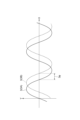
- FIG. 2 is a side view of the electromagnetic wave reflecting structure according to the embodiment.
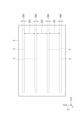
- FIG. 2 is a plan view of the electromagnetic wave reflecting structure according to the embodiment.
- 13 is a diagram illustrating an embodiment in which the phases of the periods of periodic concaves and convexes along the X-axis direction are different in a plurality of conductive portions;
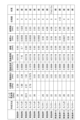
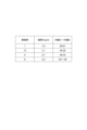
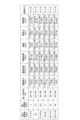
- FIG. FIG. 1 is a table showing the preparation methods, structural parameters, materials, and measured property values of Examples 1 to 14.
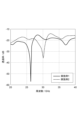
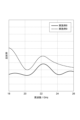
- FIG. 1 is a diagram showing frequency dependence of transmittance based on the measurement results of Examples 1 and 2.
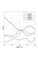
- FIG. 1 is a diagram showing frequency dependence of transmittance based on the measurement results of Examples 1, 3, and 4.
- FIG. 1 is a diagram showing the thickness of silver constituting the conductive portion and the minimum transmittance value (dB) based on the measurement results of Examples 1, 12, 5, and 6.
- FIG. 13 is a diagram showing frequency dependence of reflectance based on the measurement results of Examples 7, 13, 8, and 10.
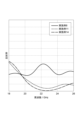
- FIG. 13 is a diagram showing frequency dependence of reflectance based on the measurement results of Examples 8 and 9.
- FIG. 13 is a diagram showing frequency dependence of reflectance based on the measurement results of Examples 8, 11, and 14.
- 11 is a diagram showing preferred ranges of structural parameters of a plurality of conductive parts for each target characteristic value of an electromagnetic wave reflecting structure.
- FIG. 1 is a perspective view showing an electromagnetic wave reflecting structure according to this embodiment
- FIG. 2 is a side view of the electromagnetic wave reflecting structure according to this embodiment
- FIG. 3 is a plan view of the electromagnetic wave reflecting structure according to this embodiment.
- a Cartesian coordinate system C consisting of an X-axis, a Y-axis, and a Z-axis is shown.
- the electromagnetic wave reflecting structure 1 includes a plurality of conductive parts 3 and a support substrate part 5.
- the support substrate part 5 is indicated by a two-dot chain line.
- Each of the plurality of conductive parts 3 is made of a conductive material, and is a linear element having periodic irregularities along the X-axis direction, which is a first direction.
- the plurality of conductive parts 3 are arranged in sequence at approximately equal intervals along the Z-axis direction, which is a second direction.
- the height direction of the periodic irregularities of each conductive part 3, i.e., the direction of the irregularities, is along the Y-axis direction, which is a third direction.
- each conductive part 3 have a shape in which a linear member extending in the X-axis direction is periodically bent alternately in the positive Y-axis direction and the negative Y-axis direction along the X-axis direction.
- the angle between the height direction of the periodic unevenness of each conductive portion 3 and the Y-axis direction is 20 degrees or less, the height direction of the periodic unevenness of each conductive portion 3 can be considered to be along the Y-axis direction.
- the angle is preferably 10 degrees or less, more preferably 5 degrees or less, even more preferably 3 degrees or less, and even more preferably 1 degree or less.
- the conductive materials constituting the plurality of conductive parts 3 may be materials each having electrical conductivity.
- the conductivity of the conductive material is preferably 1.0 ⁇ 10 S/cm or more, more preferably 1 ⁇ 10 2 S/cm or more, even more preferably 1 ⁇ 10 4 S/cm or more, and even more preferably 1 ⁇ 10 5 S/cm or more.
- Examples of conductive materials constituting the conductive parts 3 that may have such conductivity include metals such as copper, silver, aluminum, gold, nickel, iron, tin, tungsten, and molybdenum, alloys containing any of these metals, carbon materials such as carbon nanotubes and fullerene-based materials, conductive polymers such as I2-doped polyacetylene, and charge transfer complexes (TTF-TCNQ).
- metals such as copper, silver, aluminum, gold, nickel, iron, tin, tungsten, and molybdenum, alloys containing any of these metals, carbon materials such as carbon nanotubes and fullerene-based materials, conductive polymers such as I2-doped polyacetylene, and charge transfer complexes (TTF-TCNQ).
- the conductive material constituting the multiple conductive parts 3 may be a polymeric material in which multiple metal particles are dispersed.
- the multiple metal particles may be present in a dispersed state in the polymeric material, or may be present as aggregates in the polymeric material.
- the metal particles may be composed of at least one metal selected from the group consisting of copper, silver, aluminum, gold, nickel, iron, tin, tungsten, and molybdenum and/or at least one alloy containing the at least one metal.
- the particle diameter of the metal particles may be, for example, 10 nm or more and 100 ⁇ m or less.
- the shape of the metal particles may be, for example, spherical, cubic, flat, polyhedral, strip-like, etc.
- the polymeric material may be, for example, at least one resin selected from the group consisting of (meth)acrylic resins, styrene resins, vinyl resins, polyolefin resins, polyester resins, polyurethane resins, polyamide resins, polycarbonate resins, epoxy resins, and silicone resins.
- the supporting substrate 5 supports the conductive parts 3 so as to maintain the relative positional relationship of the conductive parts 3. In this embodiment, such support is achieved by embedding the conductive parts 3 entirely within the supporting substrate 5.
- the electromagnetic wave reflecting structure 1 is a plate-like member having a thickness direction in the Y-axis direction and a substantially flat front surface 5S and back surface 5R extending along the XZ plane defined by the X-axis and Z-axis.
- the supporting substrate 5 defines the external shape of such an electromagnetic wave reflecting structure 1.
- the support substrate 5 is made of an organic material such as acrylic, polyethylene terephthalate (PET), polycarbonate (PC), fluorinated polyimide, polypropylene, cycloolefin copolymer (COC), cycloolefin polymer (COP), polytetrafluoroethylene (PTFE), polyimide, etc. Therefore, the support substrate 5 can be easily formed to have a conformal shape with respect to the conductive portion 3, i.e., a shape that follows the shape of the conductive portion 3, so that the support substrate 5 can stably support a plurality of conductive portions 3.
- organic material such as acrylic, polyethylene terephthalate (PET), polycarbonate (PC), fluorinated polyimide, polypropylene, cycloolefin copolymer (COC), cycloolefin polymer (COP), polytetrafluoroethylene (PTFE), polyimide, etc. Therefore, the support substrate 5 can be easily formed to have a conformal shape with
- the support substrate 5 is preferably made of an organic material with a low dielectric constant such as polypropylene, cycloolefin copolymer (COC), cycloolefin polymer (COP), polytetrafluoroethylene (PTFE), polyimide, etc.
- the support base material 5 is made of an organic material with high transmittance to visible light, such as acrylic, polyethylene terephthalate (PET), polycarbonate (PC), or fluorinated polyimide.
- the support substrate 5 may also be made of a material other than an organic material, for example a glass material such as soda glass, or a low dielectric constant oxide material such as alumina.
- each conductive portion 3 when viewed from the positive direction of the Z axis, each conductive portion 3 has a sinusoidal shape with a period of 3 ⁇ along the X axis direction as the periodic unevenness.
- Each conductive portion 3 also has a bending angle 3 ⁇ , which is a structural parameter related to the degree of bending of the periodic unevenness.
- the bending angle 3 ⁇ is defined as the angle formed by an imaginary line 3B that passes through a center point 3N in the Y axis direction and extends parallel to the X axis, and an imaginary line 3Q that extends from a peak point 3P in the Y axis direction to the center point 3N, in one period of each conductive portion 3.
- each conductive portion 3 has a bending height 3H, which is a structural parameter related to the degree of the magnitude of the periodic unevenness.
- the bending height 3H is defined as the length in the Y-axis direction from the peak point in the positive Y-axis direction to the peak point in the negative Y-axis direction in one period of each conductive portion 3, as viewed from the positive Z-axis direction.
- each conductive portion 3 has a thickness 3T.
- the thickness 3T is defined as the length in a direction perpendicular to the extension direction of each portion of each conductive portion 3, as viewed from the positive Z-axis direction.
- the shape of the cross section perpendicular to the extension direction of each conductive portion 3 is not particularly limited, and can be, for example, a circle, an ellipse, or a rectangle.
- the periodic unevenness of the multiple conductive parts 3 has the same period 3 ⁇ . Furthermore, the phase of the period of the periodic unevenness along the X-axis direction is the same in the multiple conductive parts 3. That is, the phase difference of the period of the periodic unevenness along the X-axis direction in the multiple conductive parts 3 is 0 degrees. Therefore, as shown in Figure 1, the peak line A3 passing through the peak point on the negative side of the Y-axis of each conductive part 3 and the closest peak point of the adjacent conductive part 3 forms a straight line along the Z-axis direction.
- each of the conductive portions 3 when viewed from the negative Y-axis direction, each of the conductive portions 3 is spaced apart from adjacent conductive portions 3 by a distance S3 along the Z-axis direction. Each conductive portion 3 has a width 3W along the Z-axis direction.
- each conductive portion 3 exhibits a magnetic response to the magnetic field of the incident electromagnetic wave that is the same as or similar to that of multiple split ring resonators arranged periodically along the X-axis direction.
- a split ring resonator is a resonator that forms a series circuit of a coil and a capacitor by providing a gap in a ring portion made of a conductive material, and has a coil capacitance C and a capacitor inductance L that are determined by the material and shape.
- each conductive portion 3 can be considered to constitute a plurality of pseudo split ring resonators arranged periodically along the X-axis direction. More specifically, each conductive portion 3 can be considered to constitute a pseudo split ring resonator with a gap on the positive Y-axis side and a pseudo split ring resonator with a gap on the negative Y-axis side, arranged periodically and alternately along the X-axis direction.
- the conductive parts 3 are arranged in sequence along the Z-axis direction, so that the conductive parts 3 can be considered to constitute a plurality of pseudo split ring resonators arranged along the XZ plane defined by the X-axis direction and the Z-axis direction.
- the height direction of the periodic unevenness of the conductive parts 3 is along the Y-axis direction. Therefore, for example, when an electromagnetic wave EM having an oscillating electric field and an oscillating magnetic field as shown in FIG.
- the electromagnetic wave reflecting structure 1 is incident on the electromagnetic wave reflecting structure 1 so as to intersect with the XZ plane, that is, when the electromagnetic wave EM is incident on the electromagnetic wave reflecting structure 1 so as to intersect with the surface 5S of the electromagnetic wave reflecting structure 1, if the height direction of the periodic unevenness of the conductive parts 3 is along the XZ plane defined by the X-axis direction and the Z-axis direction, the oscillating magnetic field of the electromagnetic wave EM does not penetrate the ring of the pseudo split ring resonator, whereas at least a part of the oscillating magnetic field of the electromagnetic wave EM actually penetrates the ring of the pseudo split ring resonator and generates a current in the ring.
- the electromagnetic wave reflecting structure 1 when electromagnetic waves EM of a predetermined high frequency are incident on the electromagnetic wave reflecting structure 1 in this manner, LC resonance occurs in each pseudo split ring resonator, restricting the intrusion of the electromagnetic waves EM and reflecting the electromagnetic waves EM. Since the unevenness of each conductive portion 3 is periodically arranged, the resonance frequencies generated in each pseudo split ring resonator are the same or close to each other. Therefore, the electromagnetic wave reflecting structure 1 of this embodiment exhibits a high reflectance to electromagnetic waves in a high frequency band including such high frequencies. The relative positional relationship of these multiple pseudo split ring resonators is maintained by the support substrate portion 5.
- the frequency band of the electromagnetic waves EM reflected by the electromagnetic wave reflecting structure 1 may be 1 GHz to 300 GHz, and preferably 20 GHz to 40 GHz. It is preferable that the electromagnetic wave reflecting structure 1 selectively reflects electromagnetic waves EM in a predetermined frequency band, for example, the above-mentioned frequency band of 1 GHz to 300 GHz, preferably 20 GHz to 40 GHz.
- the transmittance of the electromagnetic wave reflecting structure 1 for electromagnetic waves other than the frequency band is sufficiently higher than the transmittance for electromagnetic waves EM in the frequency band, so that the electromagnetic wave reflecting structure 1 sufficiently transmits electromagnetic waves other than the frequency band.
- each of the multiple conductive parts 3 is made of a metal.
- the period 3 ⁇ of the periodic unevenness of the multiple conductive parts 3 is the same, and the phase of the period of the periodic unevenness along the X-axis direction is the same in the multiple conductive parts 3. This causes a particularly strong LC resonance to occur in the entire multiple pseudo split ring resonators, making it possible to particularly increase the reflectance of the electromagnetic wave reflecting structure 1.
- each bending angle 3 ⁇ of the periodic unevenness of at least some of the multiple conductive parts 3 is 0.1 radians or more and 1.0 radians or less, and it is more preferable that each bending angle 3 ⁇ of the periodic unevenness of all of the multiple conductive parts 3 is 0.1 radians or more and 1.0 radians or less. It is more preferable that each bending angle 3 ⁇ is 0.2 radians or more, and it is particularly preferable that it is 0.4 radians or more. As a result, a strong LC resonance occurs in the pseudo split ring resonator, and the reflectance of the electromagnetic wave reflecting structure 1 can be particularly large.
- the thickness 3T of at least a part of the conductive parts 3 among the plurality of conductive parts 3 is preferably 0.0003 mm or more, more preferably 0.0008 mm or more, and particularly preferably 0.0022 mm or more.
- the thickness 3T of all of the plurality of conductive parts 3 is more preferably 0.0003 mm or more, more preferably 0.0008 mm or more, and particularly preferably 0.0022 mm or more.
- the thickness 3T of at least a part of the conductive parts 3 among the plurality of conductive parts 3 is preferably 1.5 mm or less, and more preferably 1.5 mm or less. As a result, it becomes easy to maintain the gap portion of the pseudo split ring resonator necessary to obtain sufficient resonance strength.
- the distance S3 between at least some of the conductive parts 3 and adjacent conductive parts 3 along the Z-axis direction can be 1.35 mm or more and 6.2 mm or less, and in particular, the distance S3 between all of the conductive parts 3 and adjacent conductive parts 3 along the Z-axis direction can be 1.35 mm or more and 6.2 mm or less.
- the distance S3 may be 2.00 mm or more, preferably 4.00 mm or more, and more preferably 6.00 mm or more.
- the width 3W along the Z-axis direction of at least some of the multiple conductive parts 3 can be 0.45 mm or more and 1.4 mm or less, and in particular the width 3W along the Z-axis direction of all of the multiple conductive parts 3 can be 0.45 mm or more and 1.4 mm or less.
- the period 3 ⁇ of the periodic unevenness of the multiple conductive parts 3 is the same, and the phase of the period of the periodic unevenness along the X-axis direction is the same in the multiple conductive parts 3 (see Figures 1 and 2), but the phase of the period of the periodic unevenness along the X-axis direction may be different in the multiple conductive parts 3.
- FIG. 4 is a diagram showing a modified example in which the phase of the periodic unevenness in the X-axis direction differs in the multiple conductive parts 3.
- the shape of one conductive part 3A of the multiple conductive parts 3 as viewed from the positive direction of the Z-axis is shown by a solid line
- the shape of one conductive part 3B adjacent to conductive part 3A among the multiple conductive parts 3 is shown by a dashed line.
- the period of the periodic unevenness along the X-axis direction in the conductive portion 3A and the conductive portion 3B is shifted by 3 ⁇ .
- the magnitude of this 3 ⁇ is less than 1/4 of the period 3 ⁇ . That is, the phase difference of the period of the periodic unevenness along the X-axis direction in the conductive portion 3A and the conductive portion 3B is less than 90°.
- This relationship is satisfied between all two adjacent conductive portions 3 in the multiple conductive portions 3.
- strong LC resonance occurs throughout the multiple pseudo split ring resonators, so that the reflectance of the electromagnetic wave reflection structure 1 can be increased.
- the phase difference is less than 90°, and more preferably approximately 0 degrees (as in the case of the basic embodiment described above).
- the multiple conductive parts 3 are linear elements, but they may also have a band-like shape with the Z-axis direction as the width direction.
- the distance S3 between two adjacent pairs of conductive parts 3 along the Z-axis direction is the same for all pairs, i.e., the multiple conductive parts 3 are arranged at equal intervals along the Z-axis direction (see FIG. 3), but some or all of the multiple conductive parts 3 may be arranged at different intervals along the Z-axis direction.
- the entirety of the multiple conductive parts 3 is embedded in the support substrate 5 (see FIG. 1), but only a portion of the multiple conductive parts 3 may be embedded in the support substrate 5.
- a portion of the multiple conductive parts 3 in the negative Y-axis direction may be located outside the surface 5S of the support substrate 5, and the remaining portions of the multiple conductive parts 3 may be embedded in the support substrate 5.
- the portion of the multiple conductive parts 3 and the support substrate 5 define the external shape of the electromagnetic wave reflecting structure 1.
- the concave portions i.e., the portions of each conductive portion 3 that constitute the above-mentioned "pseudo split ring resonator with a gap on the positive Y-axis side
- convex portions i.e., the portions of each conductive portion 3 that constitute the above-mentioned "pseudo split ring resonator with a gap on the negative Y-axis side
- the periodic unevenness of each conductive portion 3 are preferably embedded in the support substrate 5, and more preferably embedded in the support substrate 5.
- the concave portions and the convex portions are covered with different materials, they will be covered with media having different dielectric constants, and there is a possibility that a shift will occur in the resonant frequency of the resonance generated by the concave portions and the convex portions.
- the concave portions and the convex portions in the above-mentioned form, it is possible to prevent or suppress such a shift in the resonant frequency.
- each conductive portion 3 when viewed from the positive direction of the Z axis, has a sinusoidal shape with a period of 3 ⁇ along the X axis direction as a periodic unevenness (see Figure 2), but the periodic unevenness may have other shapes, for example, a periodic rectangular unevenness shape.
- Figure 5 is a diagram showing the creation methods, structural parameters, materials, and measured characteristic values of Examples 1 to 14.
- the "bending height,” “bending angle,” “bending period,” “line width,” “line thickness,” “line spacing,” and “phase difference” in Figure 5 correspond to the “bending height 3H” (see Figure 2), “bending angle 3 ⁇ ” (see Figure 2), “period 3 ⁇ ” (see Figure 2), “width 3W” (see Figure 3), “thickness 3T” (see Figure 2), “distance S3” (see Figure 3), and “phase difference corresponding to 3 ⁇ ” (see Figure 4) in the above embodiment, respectively.
- the inventors of the present application created electromagnetic wave reflecting structures by sputtering as Examples 1 to 6 and 12. Specifically, an acrylic resin plate was created by a 3D printer, the surface of which had multiple uneven depressions extending in a first direction, the shapes of which correspond to the multiple conductive parts 3 of the above embodiment and the shapes of which correspond to the structural parameters shown in FIG. 5. A mask was then formed on the areas of the surface of the acrylic resin plate where the multiple uneven depressions were not formed, and a silver film was formed in the uneven depressions by sputtering, thereby forming multiple conductive parts made of silver. In this way, the electromagnetic wave reflecting structures of Examples 1 to 6 and 12, which have multiple conductive parts made of silver and a support substrate part made of acrylic resin, were created.
- the inventors of the present application created electromagnetic wave reflecting structures in Examples 7 to 11, 13, and 14 by embedding metal wires.
- an acrylic resin plate was created in the same manner as in Examples 1 to 6 and 12. Then, metal wires were embedded in the multiple recesses of the unevenness of the acrylic resin plate.
- the wires used in Examples 7 and 13 were made of silver
- the wires used in Examples 8, 10, 11, and 14 were made of copper
- the wires used in Example 9 were made of aluminum.
- electromagnetic wave reflecting structures according to Examples 7 to 11, 13, and 14 were created, each having multiple conductive parts made of silver, copper, or aluminum and a supporting substrate part made of acrylic resin.
- the S parameters were measured using electromagnetic waves from 18 GHz to 100 GHz by the free space method, and the transmittance and reflectance for the electromagnetic waves were evaluated.
- Figure 6 is a diagram showing the frequency dependence of transmittance based on the measurement results of Examples 1 and 2.
- the electromagnetic wave reflecting structure of Example 1 had a peak reflectance (minimum transmittance) when the electromagnetic wave frequency was about 26 GHz, and the half-value width of the peak was 2.29 GHz.
- the electromagnetic wave reflecting structure of Example 2 had a peak reflectance (minimum transmittance) when the electromagnetic wave frequency was about 30 GHz, and the half-value width of the peak was 1.99 GHz.
- a comparison of Examples 1 and 2 showed that when the shape of the periodic unevenness of the conductive portion was reduced in size while maintaining a similar shape, the frequency at which the reflectance peaked shifted to the higher frequency side.
- Figure 7 is a diagram showing the frequency dependence of transmittance based on the measurement results of Examples 1, 3, and 4.
- Figure 8 shows the relationship between the thickness of the silver constituting the conductive part and the minimum transmittance value (dB) based on the measurement results of Examples 1, 12, 5, and 6.
- the resonance peak intensity was less than -30 dB. Comparing the measurement results of Examples 1, 12, 5, and 6, it was found that as the conductive part becomes thicker, the minimum transmittance value (dB) becomes smaller, i.e., the reflectance becomes larger.
- Figure 9 is a diagram showing the frequency dependence of reflectance based on the measurement results of Examples 7, 13, 8, and 10. Comparing the measurement results of Examples 7, 13, 8, and 10, it was found that as the line spacing (distance S3 in the embodiment) becomes smaller, the peak value of reflectance increases and the frequency at which the reflectance peaks shifts to the higher frequency side.
- Figure 10 shows the frequency dependence of reflectance based on the measurement results of Examples 8 and 9. Comparing the measurement results of Examples 8 and 9, it was found that the reflectance of an electromagnetic wave reflecting structure whose conductive portion is made of aluminum is greater than the reflectance of an electromagnetic wave reflecting structure whose conductive portion is made of copper.
- Figure 11 shows the frequency dependence of reflectance based on the measurement results of Examples 8, 11, and 14. Comparing the measurement results of Examples 8, 11, and 14, it was found that in multiple conductive parts, the smaller the phase difference in the period of the periodic unevenness of two adjacent conductive parts, the greater the reflectance.
- Figure 12 is a diagram showing the preferred ranges of structural parameters of multiple conductive parts for each target characteristic value (target frequency, target half-width, and target reflectivity) of the electromagnetic wave reflecting structure, determined based on the above measurement results of Examples 1 to 14 and theoretical considerations.
- the "target frequency” in Figure 12 is the target value of the frequency at which the reflectivity peaks in the electromagnetic wave frequency dependence of the reflectivity
- the "target half-width” is the target value of the half-width of the peak of the reflectivity
- the “target reflectivity” is the target value of the reflectivity at the peak of the reflectivity.
- the lower limit of the "bending angle” was determined based on the measurement results of Examples 1, 3 and 4 shown in Figure 7
- the lower limit of the "line thickness” was determined based on the measurement results of Examples 1, 12, 5 and 6 shown in Figure 8
- the lower limit of the "line spacing” was determined based on the measurement results of Examples 7, 13, 8 and 10 shown in Figure 9
- the upper limit of the "periodic deviation” was determined based on the measurement results of Examples 8, 11 and 14 shown in Figure 11.
- the lower and upper limits of the other structural parameters were determined to correspond to the range in which the desired characteristics are expected to be obtained, based on the value in parentheses that is considered to be the most preferable.
- the structural parameters of electromagnetic wave reflecting structures with target frequencies other than 30 GHz i.e., electromagnetic wave reflecting structures with target frequencies of 2.7 to 5.4 GHz, 37 to 43.5 GHz, 76 to 78 GHz, 92 to 114 GHz, and 130 to 174 GHz, were determined based on the ratio between those target frequencies and a frequency of 30 GHz by expanding or contracting the preferred numerical range of the structural parameters determined for an electromagnetic wave reflecting structure with a target frequency of 30 GHz, where the preferred range is considered to change based on the ratio.
- the electromagnetic wave reflecting structure of the present disclosure has the following configuration.
- a plurality of linear or strip-shaped conductive parts made of a conductive material and having periodic unevenness along a first direction, the conductive parts being sequentially arranged along a second direction perpendicular to the first direction;
- each of the plurality of conductive parts is made of a metal.
- the periods of the periodic unevenness of the plurality of conductive portions are substantially the same as one another,
- Electromagnetic wave reflecting structure 3... Conductive part, 5... Support base material part.
Landscapes
- Physics & Mathematics (AREA)
- Electromagnetism (AREA)
- Engineering & Computer Science (AREA)
- Microelectronics & Electronic Packaging (AREA)
- Aerials With Secondary Devices (AREA)
- Shielding Devices Or Components To Electric Or Magnetic Fields (AREA)
Abstract
本発明の電磁波反射構造体1は、導電性材料からなり、第1の方向に沿って周期的な凹凸を有する線状又は帯状の複数の導電部3であって、第1の方向と直交する第2の方向に沿って順に配置された複数の導電部3と、複数の導電部3を支持する支持基材部5と、を備える。複数の導電部3の周期的な凹凸の高さ方向は、第1の方向及び第2の方向に直交する第3の方向に沿っている。
Description
本発明は、電磁波反射構造体に関する。
データ通信の高速大容量化に伴い、使用される電磁波が高周波数化している。高周波数の電磁波は、直進性が高く、損失性媒質となるものが多いことから、遮蔽物によって通信の品質が低下したり通信が不可能となったりするエリアが生じやすい。このような問題を解決するために、高周波数の電磁波を反射する機能を有する反射構造体を適切な位置に配置することによって、電磁波を当該反射構造体で反射させて、そのようなエリアに伝搬させる方法がある。
下記特許文献1には、平面視で、周期的な凹凸形状、具体的には正弦波の波形状に湾曲した複数の導電性線状体を利用した反射フィルムが記載されている。当該複数の導電性線状体は、反射フィルムの面内方向に周期的に凹凸している。また、下記特許文献2には、基材の表面に対して所定角度に傾斜した複数の反射面を有する電磁波反射層を利用した電波吸収体が記載されている。この反射面は、電磁波反射層の厚さ方向に周期的に凹凸している単一の帯状体と見ることができ、この反射面を有する電磁波反射層は、基材の面上に設けられている。
上述の特許文献1、2に記載されているような従来の電磁波を反射するための構造体は、電磁波の反射のために周期的に屈曲した凹凸形状を有する導電性線状体又は帯状体を利用しているが、所定の高周波帯域の電磁波の反射率を十分に高くすることが困難であった。
本発明は上述の課題に鑑みてなされたものであり、所定の高周波帯の電磁波に対する高い反射率を実現することが可能な電磁波反射構造体を提供することを目的とする。
上述の課題を解決するため、本発明に係る電磁波反射構造体は、導電性材料からなり、第1の方向に沿って周期的な凹凸を有する線状又は帯状の複数の導電部であって、第1の方向と直交する第2の方向に沿って順に配置された複数の導電部と、上記複数の導電部を支持する支持基材部と、を備え、上記複数の導電部の上記周期的な凹凸の高さ方向は、第1の方向及び第2の方向に直交する第3の方向に沿っている。
本発明に係る電磁波反射構造体では、周期的な凹凸を有する各導電部は、入射した電磁波の磁場に対して、第1の方向に沿って周期的に配置された複数の分割リング共振器と同様又は類似の磁気応答を示す。そのため、各導電部は、第1の方向に沿って周期的に配置された複数の疑似分割リング共振器を構成しているとみなすことができる。そして、そのような導電部が第2の方向に沿って順に配置されているため、複数の導電部は、第1方向と第2方向によって規定される平面に沿って配置された複数の疑似分割リング共振器を構成するとみなすことができる。これらの複数の疑似分割リング共振器は、支持基材部によって、相対的な位置関係が維持される。そして、複数の導電部の周期的な凹凸の高さ方向は、第3の方向に沿っているため、電磁波が、第1方向と第2方向によって規定される平面に交差するように電磁波反射構造体に入射すると、当該電磁波の振動磁場の少なくとも一部は、上記疑似分割リング共振器のリングを貫き、当該リングに電流を発生する。
そのため、所定の高周波数の電磁波がそのように電磁波反射構造体に入射すると、上記疑似分割リング共振器においてLC共振が生じ、当該電磁波の侵入を制限して当該電磁波を反射するようになる。そのため、電磁波反射構造体は、そのような高周波数を含む高周波数帯の電磁波に対して大きな反射率を示す。電磁波反射構造体が反射する当該電磁波の周波数帯は、1GHz~300GHzであってよく、20GHz~40GHzが好ましい。
さらに、本発明に係る電磁波反射構造体では、複数の導電部が、それぞれ金属からなることができる。これにより、上記疑似分割リング共振器において強いLC共振が生じるため、電磁波反射構造体の上記反射率を特に大きくすることができる。
さらに、本発明に係る電磁波反射構造体では、複数の導電部の周期的な凹凸の周期が互いに略同一であり、複数の導電部の隣り合う2つの導電部の当該周期の位相差が、90°未満であることができる。これにより、複数の疑似分割リング共振器全体において強いLC共振が生じるため、電磁波反射構造体の上記反射率を大きくすることができる。
さらに、本発明に係る電磁波反射構造体では、複数の導電部のうちの少なくとも一部の導電部の周期的な凹凸の各屈曲角度が、0.1ラジアン以上、1.0ラジアン以下であることができる。これにより、上記疑似分割リング共振器において強いLC共振が生じるため、電磁波反射構造体の上記反射率を特に大きくすることができる。
さらに、本発明に係る電磁波反射構造体では、前記複数の導電部のうちの少なくとも一部の導電部の厚さが、0.0003mm以上であることができる。これにより、上記疑似分割リング共振器において強いLC共振が生じるため、電磁波反射構造体の上記反射率を特に大きくすることができる。
さらに、本発明に係る電磁波反射構造体では、複数の導電部のうちの少なくとも一部の導電部は、隣り合う導電部と第2の方向に沿って1.35mm以上、6.2mm以下離間していることができる。これにより、30GHz近傍の周波数の電磁波によって上記疑似分割リング共振器においてLC共振が生じ易くすることができるため、30GHz近傍の高周波数帯の電磁波に対する反射率を特に大きくし易くなる。
さらに、本発明に係る電磁波反射構造体では、複数の導電部のうちの少なくとも一部の導電部の第2の方向に沿った幅が、0.45mm以上、1.4mm以下であることができる。これにより、30GHz近傍の周波数の電磁波によって上記疑似分割リング共振器においてLC共振が生じ易くすることができるため、30GHz近傍の高周波数帯の電磁波に対する反射率を特に大きくし易くなる。
本発明によれば、所定の高周波帯の電磁波に対する高い反射率を実現することが可能な電磁波反射構造体が提供される。
以下、添付図面を参照して、本発明を実施するための形態を詳細に説明する。なお、各図面において、可能な場合には同一要素には同一符号を用いる。また、図面中の構成要素内及び構成要素間の寸法比は、図面の見易さのため、それぞれ任意となっている。
図1は、本実施形態に係る電磁波反射構造体を示す斜視図であり、図2は、本実施形態に係る電磁波反射構造体の側面図であり、図3は、本実施形態に係る電磁波反射構造体の平面図である。図1及び必要に応じて以降の図においては、X軸、Y軸及びZ軸から構成される直交座標系Cが示されている。
図1~図3に示すように、本実施形態に係る電磁波反射構造体1は、複数の導電部3と、支持基材部5を備える。図1では、支持基材部5は二点鎖線で示されている。複数の導電部3は、それぞれ導電性材料からなり、第1の方向であるX軸方向に沿って周期的な凹凸を有する線状の要素である。複数の導電部3は、第2の方向であるZ軸方向に沿って順に略等間隔で配置されている。各導電部3の周期的な凹凸の高さ方向、即ち凹凸する方向は、第3の方向であるY軸方向に沿っている。即ち、各導電部3の周期的な凹凸は、X軸方向に延びる線状の部材が、X軸方向に沿って、Y軸正方向とY軸負方向に交互に周期的に屈曲した形状を有する。
ここで、各導電部3の周期的な凹凸の高さ方向とY軸方向とが成す角度が20度以下であれば、各導電部3の周期的な凹凸の高さ方向がY軸方向に沿っていると見做すことができる。後述のように電磁波反射構造体1に入射した電磁波EMの振動磁場の少なくとも一部が、疑似分割リング共振器のリングを貫き易くなる観点から、当該角度は10度以下であることが好ましく、5度以下であることがさらに好ましく、3度以下であることがさらに好ましく、1度以下であることがさらに、好ましい。
複数の導電部3を構成する導電性材料は、それぞれ電気伝導性を有する材料であればよい。当該導電性材料の導電率(電気伝導率)が高いほど、後述の電磁波反射構造体1の電磁波EMに対する反射率を高くすることができる。その観点から、当該導電性材料の導電率は、1.0×10S/cm以上であることが好ましく、1×102S/cm以上であることがより好ましく、1×104S/cm以上であることがさらに好ましく、1×105S/cm以上であることがさらに好ましい。このような導電率を有し得る導電部3を構成する導電性材料として、例えば、銅、銀、アルミニウム、金、ニッケル、鉄、スズ、タングステン、モリブデン等の金属、これらの金属のいずれかを含む合金、カーボンナノチューブ及びフラーレン系材料等のカーボン材料、I2ドープポリアセチレン等の導電性高分子、及び電荷移動錯体(TTF-TCNQ)を挙げることができる。
また、複数の導電部3を構成する導電性材料は、複数の金属粒子が分散された高分子材であってよい。当該複数の金属粒子は、当該高分子材中で離散して存在してもよいし、当該高分子材中で凝集して凝集体として存在してもよい。当該金属粒子は、例えば、銅、銀、アルミニウム、金、ニッケル、鉄、スズ、タングステン、及びモリブデンからなる群から選択される少なくとも1種の金属及び/又は、当該少なくとも1種の金属を含む少なくとも1種の合金で構成されていてよい。当該金属粒子の粒径は、例えば、10nm以上100μm以下であってよい。当該金属粒子の形状は、例えば、球状、立方体状、平板状、多面体状、帯状等であってよい。例えば、当該金属粒子として、平均直径100nm、平均長さ10μmの銀ワイヤーを用いることができる。当該高分子材は、例えば、(メタ)アクリル系樹脂、スチレン系樹脂、ビニル系樹脂、ポリオレフィン系樹脂、ポリエステル系樹脂、ポリウレタン系樹脂、ポリアミド系樹脂、ポリカーボネート系樹脂、エポキシ系樹脂、及びシリコーン系樹脂からなる群から選択される少なくとも1種の樹脂であってよい。
支持基材部5は、複数の導電部3の相対的な位置関係を維持するように複数の導電部3を支持する。本実施形態では、複数の導電部3の全体が支持基材部5内に埋め込まれることによって、そのような支持が実現されている。本実施形態では、電磁波反射構造体1は、Y軸方向を厚さ方向とし、X軸及びZ軸によって規定されるXZ面に沿って延びる略平坦な表面5S及び裏面5Rを有する板状の部材である。支持基材部5は、そのような電磁波反射構造体1の外形形状を規定している。
支持基材部5は、例えばアクリル、ポリエチレンテレフタレート(PET)、ポリカーボネート(PC)、フッ素化ポリイミド、ポリプロピレン、シクロオレフィンコポリマー(COC)、シクロオレフィンポリマー(COP)、ポリテトラフルオロエチレン(PTFE)、ポリイミド等の有機材料で構成されている。そのため、支持基材部5を導電部3に対してコンフォーマルな形状、即ち、導電部3の形状に追随した形状を有するように容易に形成することが可能なため、支持基材部5によって複数の導電部3を安定して支持することができる。支持基材部5は、高周波帯の電磁波の吸収率を低下させる観点、及び、高周波帯の電磁波に対する支持基材部5の表面での反射率を大きくする観点から、ポリプロピレン、シクロオレフィンコポリマー(COC)、シクロオレフィンポリマー(COP)、ポリテトラフルオロエチレン(PTFE)、ポリイミド等の低誘電率の有機材料で構成されていることが好ましい。また、電磁波反射構造体1を通した視認性を確保する観点から、支持基材部5は、アクリル、ポリエチレンテレフタレート(PET)、ポリカーボネート(PC)、フッ素化ポリイミド等の可視光に対する透過率の高い有機材料で構成されていることが好ましい。
また、支持基材部5は、有機材料以外の材料、例えばソ―ダガラス等のガラス材料、アルミナ等の低誘電率酸化物材料で構成されていてもよい。
図2に示すように、Z軸正方向から見て、各導電部3は、上記周期的な凹凸として、X軸方向に沿った、周期3λの正弦波状の形状を有する。また、各導電部3は、周期的な凹凸の屈曲の程度に関連する構造パラメーターである屈曲角度3θを有する。屈曲角度3θは、Z軸正方向から見て、各導電部3の1周期分の部分において、Y軸方向の中央点3Nを通りX軸と平行に伸びる仮想線3Bと、Y軸方向のピーク点3Pから中央点3Nに伸びる仮想線3Qとが成す角度として定義される。
また、各導電部3は、周期的な凹凸の大きさの程度に関連する構造パラメーターである屈曲高さ3Hを有する。屈曲高さ3Hは、Z軸正方向から見て、各導電部3の1周期分の部分において、Y軸正方向のピーク点からY軸負方向のピーク点までのY軸方向の長さとして定義される。また、各導電部3は、厚さ3Tを有する。厚さ3Tは、Z軸正方向から見て、各導電部3の各部分における延在方向と直交する方向の長さとして定義される。各導電部3の延在方向に垂直な断面の形状は特に制限されず、例えば、円形、楕円形、矩形であることができる。
図1及び図2に示すように、複数の導電部3の周期的な凹凸は、互いに同一の周期3λを有する。さらに、複数の導電部3において、X軸方向に沿って周期的な凹凸の周期の位相が同一となっている。即ち、複数の導電部3において、X軸方向に沿った周期的な凹凸の周期の位相差は、0度となっている。そのため、図1に示すように、各導電部3のY軸負側のピーク点と、隣接する導電部3の最近接のピーク点を通るピーク線A3は、Z軸方向に沿った直線となる。
また、図3に示すように、Y軸負方向から見て、複数の導電部3はそれぞれ、隣接する導電部3とZ軸方向に沿って距離S3だけ互いに離間している。また、各導電部3は、Z軸方向に沿った幅3Wを有している。
上述のような本実施形態に係る電磁波反射構造体1では、各導電部3の周期的な凹凸は、入射した電磁波の磁場に対して、X軸方向に沿って周期的に配置された複数の分割リング共振器と同様又は類似の磁気応答を示す。分割リング共振器とは、導電性材料からなるリング部に、ギャップを設けることでコイルとコンデンサの直列回路を構成する共振器であり、その材質及び形状によって決まるコイルのキャパシタンスCとコンデンサのインダクタンスLを有する。
そのため、各導電部3は、X軸方向に沿って、周期的に配置された複数の疑似分割リング共振器を構成しているとみなすことができる。より具体的には、各導電部3は、X軸方向に沿って周期的に交互に設けられた、Y軸正方向側にギャップが設けられた疑似分割リング共振器と、Y軸負方向側にギャップが設けられた疑似分割リング共振器とを構成しているとみなすことができる。
そして、そのような導電部3がZ軸方向に沿って順に配置されているため、複数の導電部3は、X軸方向とZ軸方向によって規定されるXZ平面に沿って配置された複数の疑似分割リング共振器を構成するとみなすことができる。そして、複数の導電部3の周期的な凹凸の高さ方向は、Y軸方向に沿っている。そのため、例えば図1に示すような振動電界と振動磁界を有する電磁波EMが、XZ平面に交差するように電磁波反射構造体1に入射すると、即ち、電磁波EMが電磁波反射構造体1の表面5Sに交差するように電磁波反射構造体1に入射すると、仮に複数の導電部3の周期的な凹凸の高さ方向がX軸方向とZ軸方向によって規定されるXZ平面に沿った方向である場合には、電磁波EMの振動磁場は上記疑似分割リング共振器のリングを貫かないのに対して、実際には電磁波EMの振動磁場の少なくとも一部は、上記疑似分割リング共振器のリングを貫き、当該リングに電流を発生する。
そのため、所定の高周波数の電磁波EMがそのように電磁波反射構造体1に入射すると、各疑似分割リング共振器においてLC共振が生じ、電磁波EMの侵入を制限して電磁波EMを反射するようになる。そして、各導電部3の凹凸は周期的に設けられているため、各疑似分割リング共振器において生じる共振周波数は互いに同一となるか近接する。そのため、本実施形態の電磁波反射構造体1は、そのような高周波数を含む高周波数帯の電磁波に対して大きな反射率を示す。そして、これらの複数の疑似分割リング共振器は、支持基材部5によって、相対的な位置関係が維持される。そのため、そのような支持基材部が無い場合と比較して、上述のような大きな反射率を示す効果が安定して発揮される。電磁波反射構造体1が反射する電磁波EMの周波数帯は、1GHz~300GHzであってよく、20GHz~40GHzが好ましい。電磁波反射構造体1は、所定の周波数帯、例えば上記1GHz~300GHz、好ましくは20GHz~40GHzの周波数帯の電磁波EMを選択的に反射することが好ましい。即ち、電磁波反射構造体1は、当該周波数帯以外の電磁波を十分に透過させるように、電磁波反射構造体1の当該周波数帯以外の電磁波に対する透過率が、当該周波数帯の電磁波EMに対する透過率よりも十分に高いことが好ましい。
また、上述のように本実施形態の電磁波反射構造体1では、複数の導電部3がそれぞれ金属からなることが好ましい。複数の導電部3を構成する材料の導電率が高い程、疑似分割リング共振器において強いLC共振が生じる。そのため、複数の導電部3が金属からなることによって、電磁波反射構造体1の上記反射率を特に大きくすることができる。
さらに、上述のような本実施形態の電磁波反射構造体1では、複数の導電部3の周期的な凹凸の周期3λが互いに同一であり、複数の導電部3において、X軸方向に沿って周期的な凹凸の周期の位相が同一となっている。これにより、複数の疑似分割リング共振器全体において特に強いLC共振が生じるため、電磁波反射構造体1の上記反射率を特に大きくすることができる。
また、本実施形態の電磁波反射構造体1では、複数の導電部3のうちの少なくとも一部の導電部3の周期的な凹凸の各屈曲角度3θが、0.1ラジアン以上、1.0ラジアン以下であることが好ましく、複数の導電部3の全ての周期的な凹凸の各屈曲角度3θが、0.1ラジアン以上、1.0ラジアン以下であることがより好ましい。上記各屈曲角度3θは、0.2ラジアン以上がより好ましく、0.4ラジアン以上であることが特に好ましい。これにより、上記疑似分割リング共振器において強いLC共振が生じるため、電磁波反射構造体1の上記反射率を特に大きくすることができる。
さらに、上述のような本実施形態の電磁波反射構造体1では、複数の導電部3のうちの少なくとも一部の導電部3の上記厚さ3Tが、0.0003mm以上であることが好ましく、0.0008mm以上であることがより好ましく、0.0022mm以上であることが特に好ましい。また、複数の導電部3の全ての上記厚さ3Tが、0.0003mm以上であることがより好ましく、0.0008mm以上であることがより好ましく、0.0022mm以上であることが特に好ましい。これにより、上記疑似分割リング共振器において強いLC共振が生じるため、電磁波反射構造体1の上記反射率を特に大きくすることができる。また、上述のような本実施形態の電磁波反射構造体1では、複数の導電部3のうちの少なくとも一部の導電部3の上記厚さ3Tが、1.5mm以下であることが好ましく、複数の導電部3の全ての上記厚さ3Tが、1.5mm以下であることがより好ましい。これにより、十分な共振強度を得るために必要な疑似分割リング共振器のギャップ部分を維持することが容易となる。
さらに、上述のような本実施形態の電磁波反射構造体1では、複数の導電部3のうちの少なくとも一部の導電部3の、隣り合う導電部3とのZ軸方向に沿って離間する距離S3は、1.35mm以上、6.2mm以下とすることができ、特に複数の導電部3の全ての、隣り合う導電部3とのZ軸方向に沿って離間する距離S3は、1.35mm以上、6.2mm以下とすることができる。上記距離S3は、2.00mm以上であってもよく、4.00mm以上であることが好ましく、6.00mm以上であることがより好ましい。これにより、30GHz近傍の周波数(例えば、1GHz~300GHz又は20GHz~40GHz)の電磁波によって上記疑似分割リング共振器においてLC共振が生じ易くすることができるため、30GHz近傍の高周波数帯の電磁波に対する反射率を特に大きくし易くなる。
さらに、上述のような本実施形態の電磁波反射構造体1では、複数の導電部3のうちの少なくとも一部の導電部3のZ軸方向に沿った幅3Wが、0.45mm以上、1.4mm以下であることができ、特に複数の導電部3の全てのZ軸方向に沿った幅3Wが、0.45mm以上、1.4mm以下であることができる。これにより、30GHz近傍の周波数の電磁波によって上記疑似分割リング共振器においてLC共振が生じ易くすることができるため、30GHz近傍の高周波数帯の電磁波に対する反射率を特に大きくし易くなる。
本発明は上述の実施形態に限定されず、様々な変形態様が可能である。
例えば、上述の実施形態では、複数の導電部3の周期的な凹凸の周期3λが同一であり、複数の導電部3において、X軸方向に沿って周期的な凹凸の周期の位相が同一となっているが(図1、図2参照)、複数の導電部3において、X軸方向に沿って周期的な凹凸の周期の位相が異なっていてもよい。
図4は、複数の導電部3において、X軸方向に沿って周期的な凹凸の周期の位相が異なっている変形例の態様を模式的に示す図である。図4では、図2に対応して、Z軸正方向から見た複数の導電部3のうちの一つの導電部3Aの形状を実線で模式的に示し、複数の導電部3のうち、導電部3Aに隣接する導電部3Bの形状を破線で模式的に示している。
図4に示すように、この変形例においては、導電部3Aと導電部3Bにおいて、X軸方向に沿った周期的な凹凸の周期が、3φだけずれている。そして、この3φの大きさは、周期3λの1/4未満である。即ち、導電部3Aと導電部3Bにおいて、X軸方向に沿った周期的な凹凸の周期の位相差が、90°未満である。このような関係が、複数の導電部3における全ての隣接する2つの導電部3間において満たされている。これにより、複数の疑似分割リング共振器全体において強いLC共振が生じるため、電磁波反射構造体1の上記反射率を大きくすることができる。また、複数の導電部3のうち、X軸方向に沿った周期的な凹凸の周期の位相差が最も大きい2つの導電部3間において、当該位相差が90°未満であることが好ましく、(上述の基本実施形態の場合のように)略0度であることがさらに好ましい。
また、上述の実施形態では、複数の導電部3は線状の要素であるが、Z軸方向を幅方向とする帯状の形状を有していてもよい。
また、上述の実施形態では、隣接する2つの導電部3の組が、Z軸方向に沿って互いに離間する距離S3は、全ての組において同一である、即ち、複数の導電部3は、Z軸方向に沿って等間隔に設けられているが(図3参照)、複数の導電部3の一部又は全部が、Z軸方向に沿って異なった間隔で設けられていてもよい。
また、上述の実施形態では、複数の導電部3の全体が支持基材部5内に埋め込まれているが(図1参照)、複数の導電部3の一部のみが支持基材部5内に埋め込まれていてもよい。例えば、複数の導電部3のうち、Y軸負方向の一部が、支持基材部5の表面5Sの外部に位置し、複数の導電部3の残りの部分が支持基材部5内に埋め込まれていてもよい。この場合、複数の導電部3の当該一部と支持基材部5とが、電磁波反射構造体1の外形形状を規定する。このように複数の導電部3の少なくとも一部が支持基材部5内に埋め込まれているため、複数の導電部3同士の位置関係を維持したり、導電部3を板状ではなく線状又は帯状としたりすることが容易となる。また、各導電部3の周期的な凹凸の凹部(即ち、各導電部3のうち、上述の「Y軸正方向側にギャップが設けられた疑似分割リング共振器」を構成する部分)及び凸部(即ち、各導電部3のうち、上述の「Y軸負方向側にギャップが設けられた疑似分割リング共振器」を構成する部分)は、少なくとも一部の当該凹部及び当該凸部が支持基材部5内に埋め込まれている態様であることが好ましく、全ての当該凹部及び当該凸部が支持基材部5内に埋め込まれている態様であることがより好ましい。当該凹部及び当該凸部が互いに異なる材料によって覆われていると、それらが互いに異なる誘電率を有する媒質によって覆われることになるため、当該凹部及び当該凸部で生じる共振の共振周波数にずれが生じる可能性がある。しかし、当該凹部及び当該凸部が上記態様であることによって、そのような共振周波数のずれが生じることを、防止又は抑制することができる。
また、上述の実施形態では、Z軸正方向から見て、各導電部3は、周期的な凹凸として、X軸方向に沿った、周期3λの正弦波状の形状を有するが(図2参照)、周期的な凹凸であれば他の形状を有してもよく、例えば、周期的な矩形の凹凸形状を有してもよい。
(実施例)
以下、本発明の効果をより一層明らかなものとするため、実施例および比較例を用いて説明する。
以下、本発明の効果をより一層明らかなものとするため、実施例および比較例を用いて説明する。
本願発明者らは、実施例1~14を作成した。図5は、実施例1~14の作成方法、構造パラメーター、材質、及び測定した特性値を示す図である。図5の「屈曲高さ」、「屈曲角度」、「屈曲周期」、「線幅」、「線厚み」、「線間隔」、及び「位相差」は、上記実施形態における「屈曲高さ3H」(図2参照)、「屈曲角度3θ」(図2参照)、「周期3λ」(図2参照)、「幅3W」(図3参照)、「厚さ3T」(図2参照)、「距離S3」(図3参照)、及び「3φに対応する位相差」(図4参照)に、それぞれ対応する。
本願発明者らは、実施例1~6、12として、スパッタ法によって電磁波反射構造体を作成した。具体的には、上記実施形態の複数の導電部3に対応する形状、かつ、図5に示す構造パラメーターに対応する形状の、第1の方向に延びる複数の凹凸の窪みを表面に有するアクリル樹脂板を3Dプリンタで作成した。その後、当該アクリル樹脂板の表面の複数の凹凸の窪みが形成されていない領域上にマスクを形成し、当該凹凸の窪みにスパッタ法で銀を成膜することによって、銀で構成される複数の導電部を形成した。このようにして、銀で構成される複数の導電部とアクリル樹脂で構成される支持基材部を有する実施例1~6、12に係る電磁波反射構造体を作成した。
本願発明者らは、実施例7~11、13、14として、金属ワイヤーの埋め込みによって電磁波反射構造体を作成した。具体的には、実施例1~6、12の場合と同様に、アクリル樹脂板を作成した。その後、アクリル樹脂板の複数の凹凸の窪みに、金属からなるワイヤーを埋め込んだ。実施例7、13のワイヤーは、銀で構成されたものを用い、実施例8、10、11、14のワイヤーは、銅で構成されたものを用い、実施例9のワイヤーは、アルミニウムで構成されたものを用いた。このようにして、銀、銅、又はアルミニウムで構成される複数の導電部とアクリル樹脂で構成される支持基材部を有する実施例7~11、13、14に係る電磁波反射構造体を作成した。
続いて、実施例1~14について、フリースペース法によって18GHzから100GHzまでの電磁波を用いてSパラメーターを測定し、当該電磁波に対する透過率・反射率を評価した。
図6は、実施例1、2の測定結果に基づく、透過率の周波数依存性を示す図である。図6に示されるように、実施例1の電磁波反射構造体は、電磁波の周波数が26GHz付近で、反射率がピーク(透過率が極小)となり、そのピークの半値幅は、2.29GHzとなった。実施例2の電磁波反射構造体は、電磁波の周波数が30GHz付近で、反射率がピーク(透過率が極小)となり、そのピークの半値幅は、1.99GHzとなった。また、実施例1、2の比較から、導電部の周期的な凹凸の形状を、相似形で大きさを縮小させた場合、反射率がピークとなる周波数が高周波側にシフトすることが分かった。
図7は、実施例1、3、4の測定結果に基づく、透過率の周波数依存性を示す図である。上述のように実施例1の電磁波反射構造体は、電磁波の周波数が26GHz付近で、反射率がピーク(透過率が極小)となり、そのピークの半値幅は、2.29GHzとなった。また、図7に示されるように、実施例3の電磁波反射構造体は、電磁波の周波数が22.5GHz付近で、反射率がピーク(透過率が極小)となり、そのピークの半値幅は、2.51GHzとなった。実施例4の電磁波反射構造体は、電磁波の周波数が21GHz付近で、反射率がピーク(透過率が極小)となり、そのピークの半値幅は、2.79GHzとなった。また、実施例1、3、4の測定結果の比較から、屈曲角度を大きくすると、反射率のピークの値が大きくなると共に、半値幅が減少することが分かった。
図8は、実施例1、12、5、6の測定結果に基づく、導電部を構成する銀の厚さと、極小となる透過率の値(dB)を示す図である。実施例1、12、5、6のいずれにおいても、共振ピーク強度は-30dBより小さい値を示した。実施例1、12、5、6の測定結果の比較から、導電部が厚くなると、極小となる透過率の値(dB)が小さく、即ち、反射率が大きくなることが分かった。
図9は、実施例7、13、8、10の測定結果に基づく、反射率の周波数依存性を示す図である。実施例7、13、8、10の測定結果の比較から、線間隔(実施形態における距離S3)が小さくなると、反射率のピークの値が大きくなると共に、反射率がピークとなる周波数が高周波側にシフトすることが分かった。
図10は、実施例8、9の測定結果に基づく、反射率の周波数依存性を示す図である。実施例8、9の測定結果の比較から、導電部をアルミニウムで構成した電磁波反射構造体の反射率は、導電部を銅で構成した電磁波反射構造体の反射率よりも大きくなることが分かった。
図11は、実施例8、11、14の測定結果に基づく、反射率の周波数依存性を示す図である。実施例8、11、14の測定結果の比較から、複数の導電部において、2つの隣接する導電部の周期的な凹凸の周期の位相差が小さい方が、反射率が大きくなることが分かった。
図12は、実施例1~14の上記測定結果及び理論的な考察を基に決定した、電磁波反射構造体の目標とする特性値(狙い周波数、狙い半値幅、及び狙い反射率)ごとの、複数の導電部の構造パラメーターの好ましい範囲を示す図である。図12の「狙い周波数」は、反射率の電磁波周波数依存において、反射率がピークとなる周波数の狙い値であり、「狙い半値幅」は、当該反射率のピークの半値幅の狙い値であり、「狙い反射率」は、当該反射率のピークにおける反射率の狙い値である。また、図12の「屈曲高さ」、「屈曲角度」、「屈曲周期」、「線幅」、「線厚み」、「線間隔」、及び「周期ずれ」は、上記実施形態における「屈曲高さ3H」(図2参照)、「屈曲角度3θ」(図2参照)、「周期3λ」(図2参照)、「幅3W」(図3参照)、「厚さ3T」(図2参照)、「距離S3」(図3参照)、及び「3φに対応する位相差」(図4参照)に、それぞれ対応する。図12では、それらの構造パラメーターの好ましい数値範囲を示しており、それぞれの数値範囲の後の括弧内の数値は、それぞれの構造パラメーターの最も好ましいと考えられる値である。
狙い周波数が30GHzの電磁波反射構造体における構造パラメーターについて、「屈曲角度」の下限値については、図7に示した実施例1、3、4の測定結果を基に決定し、「線厚み」の下限値については、図8に示した実施例1、12、5、6の測定結果を基に決定し、「線間隔」の下限値については、図9に示した実施例7、13、8、10の測定結果を基に決定し、「周期ずれ」の上限値については、図11に示した実施例8、11、14の測定結果を基に決定した。他の構造パラメーターの下限値、上限値については、括弧内の最も好ましいと考えられる値を基準として、目的とする特性が得られると考えられる範囲に対応するように決定した。狙い周波数が30GHz以外の電磁波反射構造体、即ち、狙い周波数が2.7~5.4GHz、37~43.5GHz、76~78GHz、92~114GHz、及び130~174GHzの電磁波反射構造体における構造パラメーターについては、それらの狙い周波数と、周波数30GHzとの比に基づいて、狙い周波数が30GHzの電磁波反射構造体で決定した構造パラメーターの好ましい数値範囲のうち、当該比に基づいて好ましい範囲が変化すると考えられる構造パラメーターの数値範囲を拡大又は縮小することによって、決定した。
本開示の電磁波反射構造体は、以下の構成を有する。
[1] 導電性材料からなり、第1の方向に沿って周期的な凹凸を有する線状又は帯状の複数の導電部であって、前記第1の方向と直交する第2の方向に沿って順に配置された複数の導電部と、
前記複数の導電部を支持する支持基材部と、
を備え、
前記複数の導電部の前記周期的な凹凸の高さ方向は、前記第1の方向及び前記第2の方向に直交する第3の方向に沿っている、電磁波反射構造体。
[2] 前記複数の導電部が、それぞれ金属からなる、[1]に記載の電磁波反射構造体。
[3] 前記複数の導電部の前記周期的な凹凸の周期が互いに略同一であり、
前記複数の導電部の隣り合う2つの導電部の前記周期の位相差が、90°未満である、[1]又は[2]に記載の電磁波反射構造体。
[4] 前記複数の導電部のうちの少なくとも一部の導電部の前記周期的な凹凸の各屈曲角度が、0.1ラジアン以上、1.0ラジアン以下である、[1]~[3]のいずれかに記載の電磁波反射構造体。
[5] 前記複数の導電部のうちの少なくとも一部の導電部の厚さが、0.0003mm以上である、[1]~[4]のいずれかに記載の電磁波反射構造体。
[6] 前記複数の導電部のうちの少なくとも一部の導電部は、隣り合う導電部と前記第2の方向に沿って1.35mm以上、6.2mm以下離間している、[1]~[5]のいずれかに記載の電磁波反射構造体。
[7] 前記複数の導電部のうちの少なくとも一部の導電部の第2の方向に沿った幅が、0.45mm以上、1.4mm以下である、[1]~[6]のいずれかに記載の電磁波反射構造体。
1…電磁波反射構造体、3…導電部、5…支持基材部。
Claims (7)
- 導電性材料からなり、第1の方向に沿って周期的な凹凸を有する線状又は帯状の複数の導電部であって、前記第1の方向と直交する第2の方向に沿って順に配置された複数の導電部と、
前記複数の導電部を支持するsと、
を備え、
前記複数の導電部の前記周期的な凹凸の高さ方向は、前記第1の方向及び前記第2の方向に直交する第3の方向に沿っている、電磁波反射構造体。 - 前記複数の導電部が、それぞれ金属からなる、請求項1に記載の電磁波反射構造体。
- 前記複数の導電部の前記周期的な凹凸の周期が互いに略同一であり、
前記複数の導電部の隣り合う2つの導電部の前記周期の位相差が、90°未満である、請求項1又は2に記載の電磁波反射構造体。 - 前記複数の導電部のうちの少なくとも一部の導電部の前記周期的な凹凸の各屈曲角度が、0.1ラジアン以上、1.0ラジアン以下である、請求項1~3のいずれか一項に記載の電磁波反射構造体。
- 前記複数の導電部のうちの少なくとも一部の導電部の厚さが、0.0003mm以上である、請求項1~4のいずれか一項に記載の電磁波反射構造体。
- 前記複数の導電部のうちの少なくとも一部の導電部は、隣り合う導電部と前記第2の方向に沿って1.35mm以上、6.2mm以下離間している、請求項1~5のいずれか一項に記載の電磁波反射構造体。
- 前記複数の導電部のうちの少なくとも一部の導電部の第2の方向に沿った幅が、0.45mm以上、1.4mm以下である、請求項1~6のいずれか一項に記載の電磁波反射構造体。
Applications Claiming Priority (2)
| Application Number | Priority Date | Filing Date | Title |
|---|---|---|---|
| JP2023070967 | 2023-04-24 | ||
| JP2023-070967 | 2023-04-24 |
Publications (1)
| Publication Number | Publication Date |
|---|---|
| WO2024225142A1 true WO2024225142A1 (ja) | 2024-10-31 |
Family
ID=93256323
Family Applications (1)
| Application Number | Title | Priority Date | Filing Date |
|---|---|---|---|
| PCT/JP2024/015320 Ceased WO2024225142A1 (ja) | 2023-04-24 | 2024-04-17 | 電磁波反射構造体 |
Country Status (3)
| Country | Link |
|---|---|
| JP (1) | JP2024156608A (ja) |
| TW (1) | TW202446199A (ja) |
| WO (1) | WO2024225142A1 (ja) |
Families Citing this family (1)
| Publication number | Priority date | Publication date | Assignee | Title |
|---|---|---|---|---|
| WO2026110934A1 (ja) * | 2024-11-25 | 2026-05-28 | 富士フイルム株式会社 | 電波制御材料、及びレンズアンテナ |
Citations (3)
| Publication number | Priority date | Publication date | Assignee | Title |
|---|---|---|---|---|
| EP0446408A1 (de) * | 1990-03-12 | 1991-09-18 | TRUBE & KINGS KG | Reflexionsarmes Wandelement für Radarstrahlung |
| JPH08288684A (ja) * | 1995-04-20 | 1996-11-01 | K Lab:Kk | 電磁波吸収体 |
| JP2001313521A (ja) * | 2000-04-28 | 2001-11-09 | Tdk Corp | 電波減衰体 |
-
2024
- 2024-03-15 JP JP2024041427A patent/JP2024156608A/ja active Pending
- 2024-04-17 WO PCT/JP2024/015320 patent/WO2024225142A1/ja not_active Ceased
- 2024-04-18 TW TW113114443A patent/TW202446199A/zh unknown
Patent Citations (3)
| Publication number | Priority date | Publication date | Assignee | Title |
|---|---|---|---|---|
| EP0446408A1 (de) * | 1990-03-12 | 1991-09-18 | TRUBE & KINGS KG | Reflexionsarmes Wandelement für Radarstrahlung |
| JPH08288684A (ja) * | 1995-04-20 | 1996-11-01 | K Lab:Kk | 電磁波吸収体 |
| JP2001313521A (ja) * | 2000-04-28 | 2001-11-09 | Tdk Corp | 電波減衰体 |
Also Published As
| Publication number | Publication date |
|---|---|
| TW202446199A (zh) | 2024-11-16 |
| JP2024156608A (ja) | 2024-11-06 |
Similar Documents
| Publication | Publication Date | Title |
|---|---|---|
| US8179298B2 (en) | Multi-directional resonant-type electromagnetic wave absorber, method for adjusting electromagnetic wave absorption performance using the same and manufacturing method of the same | |
| US6985118B2 (en) | Multi-band horn antenna using frequency selective surfaces | |
| AU767300B2 (en) | Structure with magnetic properties | |
| US7256753B2 (en) | Synthesis of metamaterial ferrites for RF applications using electromagnetic bandgap structures | |
| US9413076B2 (en) | Electromagnetic radiation absorber | |
| CN109103603A (zh) | 基于变容二极管的有源频率选择表面结构 | |
| JP2024156608A (ja) | 電磁波反射構造体 | |
| JP2008219125A (ja) | 電波反射板及びアンテナ | |
| AU1879900A (en) | Antenna arrangements | |
| CN1575529A (zh) | 平面带隙材料 | |
| EP1421646A1 (en) | An electromagnetic window | |
| US8743017B2 (en) | Metamaterial and method for manufacturing same | |
| CN2870195Y (zh) | 一种频率选择装置 | |
| CN114300831B (zh) | 吸顶天线 | |
| CN1130796C (zh) | 带突出部的螺旋天线 | |
| JP7593862B2 (ja) | アンテナフィルム | |
| CN210537244U (zh) | 一种用于uhf频段的吸波结构和通讯设备 | |
| CN117616635A (zh) | 包括辐射器阵列和折射器件的天线装置 | |
| CN120262031A (zh) | 一种介质透镜和介质透镜天线 | |
| CN117199826A (zh) | 一种双通带频率选择表面结构 | |
| KR20240130709A (ko) | 레이더 역반사 장치에 대한 전자기 흡수재 적용 | |
| JP7845076B2 (ja) | ミリ波反射板 | |
| CN112118719B (zh) | 一种吸波单元结构 | |
| TW202616679A (zh) | 可重組智慧表面裝置 | |
| WO2025205706A1 (ja) | リフレクタ |
Legal Events
| Date | Code | Title | Description |
|---|---|---|---|
| 121 | Ep: the epo has been informed by wipo that ep was designated in this application |
Ref document number: 24796895 Country of ref document: EP Kind code of ref document: A1 |
|
| NENP | Non-entry into the national phase |
Ref country code: DE |
|
| 122 | Ep: pct application non-entry in european phase |
Ref document number: 24796895 Country of ref document: EP Kind code of ref document: A1 |