WO2024224923A1 - アンテナ装置 - Google Patents
アンテナ装置 Download PDFInfo
- Publication number
- WO2024224923A1 WO2024224923A1 PCT/JP2024/012212 JP2024012212W WO2024224923A1 WO 2024224923 A1 WO2024224923 A1 WO 2024224923A1 JP 2024012212 W JP2024012212 W JP 2024012212W WO 2024224923 A1 WO2024224923 A1 WO 2024224923A1
- Authority
- WO
- WIPO (PCT)
- Prior art keywords
- substrate
- antenna device
- antenna
- parallel
- edge
- Prior art date
- Legal status (The legal status is an assumption and is not a legal conclusion. Google has not performed a legal analysis and makes no representation as to the accuracy of the status listed.)
- Ceased
Links
Images








Classifications
-
- H—ELECTRICITY
- H01—ELECTRIC ELEMENTS
- H01Q—ANTENNAS, i.e. RADIO AERIALS
- H01Q9/00—Electrically-short antennas having dimensions not more than twice the operating wavelength and consisting of conductive active radiating elements
- H01Q9/04—Resonant antennas
- H01Q9/16—Resonant antennas with feed intermediate between the extremities of the antenna, e.g. centre-fed dipole
- H01Q9/26—Resonant antennas with feed intermediate between the extremities of the antenna, e.g. centre-fed dipole with folded element or elements, the folded parts being spaced apart a small fraction of operating wavelength
-
- H—ELECTRICITY
- H01—ELECTRIC ELEMENTS
- H01Q—ANTENNAS, i.e. RADIO AERIALS
- H01Q1/00—Details of, or arrangements associated with, antennas
- H01Q1/12—Supports; Mounting means
- H01Q1/22—Supports; Mounting means by structural association with other equipment or articles
-
- H—ELECTRICITY
- H01—ELECTRIC ELEMENTS
- H01Q—ANTENNAS, i.e. RADIO AERIALS
- H01Q1/00—Details of, or arrangements associated with, antennas
- H01Q1/27—Adaptation for use in or on movable bodies
- H01Q1/32—Adaptation for use in or on road or rail vehicles
- H01Q1/325—Adaptation for use in or on road or rail vehicles characterised by the location of the antenna on the vehicle
- H01Q1/3283—Adaptation for use in or on road or rail vehicles characterised by the location of the antenna on the vehicle side-mounted antennas, e.g. bumper-mounted, door-mounted
-
- H—ELECTRICITY
- H01—ELECTRIC ELEMENTS
- H01Q—ANTENNAS, i.e. RADIO AERIALS
- H01Q5/00—Arrangements for simultaneous operation of antennas on two or more different wavebands, e.g. dual-band or multi-band arrangements
- H01Q5/20—Arrangements for simultaneous operation of antennas on two or more different wavebands, e.g. dual-band or multi-band arrangements characterised by the operating wavebands
- H01Q5/25—Ultra-wideband [UWB] systems, e.g. multiple resonance systems; Pulse systems
-
- H—ELECTRICITY
- H01—ELECTRIC ELEMENTS
- H01Q—ANTENNAS, i.e. RADIO AERIALS
- H01Q9/00—Electrically-short antennas having dimensions not more than twice the operating wavelength and consisting of conductive active radiating elements
- H01Q9/04—Resonant antennas
- H01Q9/0407—Substantially flat resonant element parallel to ground plane, e.g. patch antenna
- H01Q9/0421—Substantially flat resonant element parallel to ground plane, e.g. patch antenna with a shorting wall or a shorting pin at one end of the element
-
- H—ELECTRICITY
- H01—ELECTRIC ELEMENTS
- H01Q—ANTENNAS, i.e. RADIO AERIALS
- H01Q9/00—Electrically-short antennas having dimensions not more than twice the operating wavelength and consisting of conductive active radiating elements
- H01Q9/04—Resonant antennas
- H01Q9/06—Details
- H01Q9/065—Microstrip dipole antennas
-
- H—ELECTRICITY
- H01—ELECTRIC ELEMENTS
- H01Q—ANTENNAS, i.e. RADIO AERIALS
- H01Q9/00—Electrically-short antennas having dimensions not more than twice the operating wavelength and consisting of conductive active radiating elements
- H01Q9/04—Resonant antennas
- H01Q9/16—Resonant antennas with feed intermediate between the extremities of the antenna, e.g. centre-fed dipole
- H01Q9/28—Conical, cylindrical, cage, strip, gauze, or like elements having an extended radiating surface; Elements comprising two conical surfaces having collinear axes and adjacent apices and fed by two-conductor transmission lines
- H01Q9/285—Planar dipole
Definitions
- This disclosure relates to an antenna device.
- Patent Document 1 discloses a system that uses a patch antenna attached to the side of a vehicle (e.g., a side sill) to perform wireless communication with a portable device carried by a user.
- a patch antenna attached to the side of a vehicle (e.g., a side sill) to perform wireless communication with a portable device carried by a user.
- the short-range communication signals are wireless signals that comply with short-range communication standards, such as Bluetooth (registered trademark) Low Energy.
- radio waves of 900 MHz or higher such as 2.4 GHz or 920 MHz (hereafter referred to as high-frequency radio waves), are used.
- Short-distance communication signals using such high-frequency radio waves have a stronger tendency to travel in a straighter direction than radio waves in the LF (low frequency) band. Therefore, a patch antenna attached along the side body has difficulty receiving direct waves (diffracted waves) from a mobile device located near the back door.
- short-range communication signals are high-frequency radio waves, they tend to be reflected by reflective objects such as the bodies and walls of other vehicles. Therefore, if there are reflective objects around the vehicle, the receiving strength of the reflected waves may exceed the receiving strength of the diffracted waves. If the receiving strength of the reflected waves is greater than the receiving strength of the diffracted waves, the distance is calculated based on the reflected wave components, which may reduce the accuracy of distance measurement. For this reason, there is a demand for an antenna with a larger gain in the horizontal direction of the board than in the vertical direction of the board so that it can receive direct waves (diffracted waves) from mobile devices that are out of line of sight.
- the vertical direction of the board here refers to the direction perpendicular to the board on which the antenna is formed, and the horizontal direction of the board refers to the direction along (parallel to) the board.
- the horizontal direction of the board refers to the direction along (parallel to) the board.
- the present disclosure has been made based on the above considerations and points of view, and one of its objectives is to provide an antenna device that can reduce its height and has a greater gain in the horizontal direction of the substrate than in the vertical direction of the substrate.
- One of the antenna devices disclosed herein comprises a substrate which is a plate-shaped dielectric, a ground plate which is a plate-shaped conductor provided on or inside the substrate, a first element which is a linear conductor element provided along the surface of the substrate, and a second element which is a linear conductor element having a three-dimensional shape, the second element including an erect portion perpendicular to the substrate and a substrate parallel portion extending from the upper end of the erect portion so as to be parallel to the substrate, the substrate parallel portion having a portion parallel to a part of the first element, and either the lower end of the erect portion or the end of the first element is connected to the power supply line, and the other is electrically connected to the ground plate.
- the current flowing in the portion of the parallel board section that is parallel to the first element acts to cancel out part of the current flowing in the first element.
- the radio waves originating from the current flowing in a direction parallel to the board are weakened, and the radio waves originating from the current flowing in the upright section are relatively stronger.
- the radio waves originating from the upright section then propagate in a direction perpendicular to the upright section, i.e., in the horizontal direction of the board.
- the gain in the horizontal direction of the board can be made greater than in the vertical direction of the board.
- the above second element has a shape in which a linear conductor element is bent midway. This makes it possible to reduce the height.
- FIG. 2 is a perspective view of an antenna device.
- FIG. 2 is a top view of the antenna device.
- FIG. 2 is a side view of the antenna device.
- FIG. 4 is a diagram conceptually showing a current distribution of a first model.
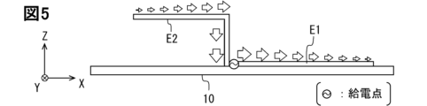
- FIG. 13 is a diagram conceptually illustrating a current distribution in a second model.
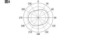
- FIG. 13 is a diagram showing the directivity of a second model.
- FIG. 13 is a diagram conceptually illustrating a current distribution in a third model.
- FIG. 13 is a diagram showing the directivity of a third model.
- FIG. 2 shows an antenna device having a support for fixing a second element.
- FIG. 13 is a diagram showing a case where a second element is fixed to a housing.
- FIG. 13 is a diagram showing a case where the second element has two standing portions.
- FIG. FIG. 13 is a diagram showing a case where the first element is formed in an L-shape.
- 11A and 11B are diagrams showing another example of the formation of the first element and the second element.
- 1A and 1B are diagrams showing the positional relationship between a cable connection end and a three-dimensional antenna.
- FIG. 1 shows an antenna device having two three-dimensional antennas.
- FIG. 1 is a diagram showing an antenna device having two three-dimensional antennas and one pattern antenna.
- FIG. 2 is a diagram showing an example of a mounting position of an antenna device in a vehicle.
- the antenna device 1 of the present disclosure is used by being attached to a moving object such as a vehicle.
- the antenna device 1 may be attached to the side (so-called side body), rear, front, roof, etc. of the vehicle.
- the antenna device 1 is used by being connected to a communication ECU (Electronic Control Unit) mounted on the vehicle via one or more cables.
- the ECU uses signals received by the antenna device 1 and can input transmission signals to the antenna device 1.
- the antenna device 1 is configured to operate in the 2.4 GHz band (2402 MHz to 2480 MHz) used by Bluetooth (registered trademark).
- the antenna device 1 may be used for only either transmission or reception. Since radio wave transmission and reception is reversible, a configuration capable of transmitting radio waves of a certain frequency is also a configuration capable of receiving radio waves of that frequency. In the following description, "transmission and reception” may be interpreted as either transmission or reception.
- the frequency band in which the antenna device 1 operates is referred to as the target frequency band.
- the frequency that is used as the reference for designing the antenna device 1 is referred to as the target frequency.
- the target frequency may be the center frequency of the target frequency band. In the following, a case will be described in which the target frequency is set to 2440 MHz.
- the target frequency may be set to a value that is slightly higher (for example, 10 MHz) than the center frequency.
- the target frequency may be set to the minimum/maximum frequency of the target frequency band.
- ⁇ represents the target wavelength, which is the wavelength of radio waves of the target frequency.
- expressions such as “ ⁇ /2” and “0.5 ⁇ ” mean half the length of the target wavelength.
- Expressions using wavelengths ( ⁇ ), such as “ ⁇ /2” and “ ⁇ /4”, are used to explain the dimensions of various members.
- the wavelength ( ⁇ ) in the description of the dimensions of the members constituting the antenna device 1 may be interpreted as the electrical length.
- the electrical length here is the effective length taking into account the fringing electric field and the wavelength shortening effect of the dielectric.
- the electrical length is sometimes called the effective length. Note that the wavelength (i.e., ⁇ ) of a 2440 MHz radio wave in a vacuum and in air is 122.8 mm.
- the expression ⁇ /4 means approximately 30.7 mm.
- the length corresponding to ⁇ /4 can be 20 mm, 25 mm, etc.
- a person skilled in the art can determine the dimensions corresponding to ⁇ /4 using a simulator or the like.
- the target frequency band may be the 2.4 GHz or 5 GHz band used by Wi-Fi (registered trademark).
- the antenna device 1 may be compatible with a frequency band used in UWB communication.
- the target frequency band may be compatible with other short-range wireless communication standards.
- the antenna device 1 includes a substrate 10, a ground plane 20, a first element 30, a second element 40, a feeder line 51, and a short-circuit line 52.
- the first element 30 and the second element 40 are designed to operate as a dipole antenna, as described below.
- a configuration including the first element 30 and the second element 40 may be referred to as an element set or a three-dimensional antenna.
- the antenna device 1 may also include components not shown in Figures 1 to 3, such as a connector, a power supply circuit, a communication IC, and a housing.
- the connector is a component for connecting a communication cable and a power supply cable.
- the communication cable is a cable for communicating with the ECU.
- the communication cable may be a coaxial cable or a feeder line.
- the power supply cable is a cable for supplying power to the antenna device 1.
- the cable may be referred to as an electric wire.
- the communication cable and the power supply cable may be bundled together as a single harness.
- the communication cable and the power supply cable may be integrated.
- the power supply circuit is a circuit that converts the voltage input from the power supply cable (e.g., battery voltage) into a voltage suitable for the operation of the communication IC and outputs it.
- the communication IC is an integrated circuit module for performing signal processing on transmitted and received signals.
- the communication IC performs, for example, modulation, demodulation, frequency conversion, amplification, etc.
- the communication IC has a ground terminal and an antenna connection terminal.
- the ground terminal is a terminal electrically connected to the base plate 20.
- the antenna connection terminal is a terminal electrically connected to the first element 30 via the power supply line 51.
- the antenna connection terminal corresponds to a terminal for transmitting and receiving high-frequency signals.
- the antenna connection terminal may be referred to as a signal terminal or a power supply terminal.
- Px shown in FIG. 1 etc. indicates the position of the antenna connection terminal.
- the position (Px) of the communication IC and the antenna connection terminal may be provided at any position on the substrate 10. Px in the figure may be interpreted as a land/location that is conductive with the antenna connection terminal.
- the substrate 10 is a plate-shaped base material on which the various circuits and the ground plate 20 described above are arranged.
- the substrate 10 may be realized using a dielectric.
- the substrate 10 may be realized using any insulating material, such as a prepreg or solder resist made by impregnating fibers such as glass or carbon with resin and hardening them.
- the substrate 10 may be a resin plate such as a printed wiring board.
- a predetermined wiring pattern may be formed on the surface of the substrate 10.
- the substrate 10 may be a multilayer substrate with one or more conductor layers formed therein.
- the substrate 10 has an area in which the base plate 20, the first element 30, the second element 40, the power supply line 51, the short circuit line 52, the connector, and the communication IC can be formed.
- the base plate 20 is formed in a rectangular shape. In other embodiments, the substrate 10 may be formed in a square, L-shape, circle, hexagon, etc.
- the substrate 10 may be provided with slits, screw holes for fixing to a housing, etc.
- the substrate 10 has a first surface and a second surface.
- the first surface is the surface on which the first element 30 is formed.
- the first surface may be referred to as the top surface.
- the second surface is the surface opposite the first surface.
- the second surface may be referred to as the back surface or bottom surface.
- the direction from the second surface to the first surface corresponds to the upward direction for the antenna device 1.
- the substrate 10 has a first edge 11, a second edge 12, a third edge 13, and a fourth edge 14.
- the first edge 11 and the second edge 12 are edges that correspond to the short sides of a rectangle.
- the first edge 11 and the second edge 12 are parallel to each other and have the same length.
- the third edge 13 and the fourth edge are edges that correspond to the long sides of a rectangle.
- the third edge 13 and the fourth edge 14 are parallel to each other and have the same length.
- the configuration of the antenna device 1 will be explained by introducing the concept of a right-handed three-dimensional coordinate system having mutually orthogonal X-, Y-, and Z-axes.
- the X-axis shown in various figures such as FIG. 1 is parallel to the longitudinal direction of the substrate 10, and the Y-axis is parallel to the lateral direction of the substrate 10.
- the Z-axis is parallel to the up-down direction.
- the direction along any one of the sides may be set as the X-axis direction.
- the direction from the first edge 11 to the second edge 12 corresponds to the positive direction of the X-axis
- the direction from the third edge 13 to the fourth edge 14 corresponds to the positive direction of the Y-axis
- the length of the substrate 10 in the X-axis direction (Lx) corresponds to the lengths of the third edge 13 and the fourth edge 14.
- the length of the substrate 10 in the Y-axis direction (Ly) corresponds to the lengths of the first edge 11 and the second edge 12.
- Lx is set to 55 mm
- Ly is set to 40 mm.
- Lx may be set to a value such as 50 mm, 60 mm, or 70 mm.
- Ly may be set to a value such as 25 mm, 30 mm, 35 mm, or 45 mm.
- the ratio of Ly to Lx (Ly/Lx) may be set to 0.4, 0.5, 0.6, etc.
- the shape of the substrate 10 may be designed to fit the mounting location.
- the ground plate 20 is a plate-shaped conductive member made of a conductive material such as copper.
- the plate-shaped member includes a thin film such as a metal foil.
- the ground plate 20 may be a conductive layer deposited by electroplating or the like on the surface of the substrate 10.
- the ground plate 20 provides a ground potential (in other words, earth potential) for the antenna device 1 by being electrically connected to the ground electrode of the power cable via, for example, a power circuit.
- the ground plane 20 is formed on the first surface of the substrate 10. In other embodiments, the ground plane 20 may be formed on the second surface or inside the substrate 10. The ground plane 20 may also be realized using a conductor layer disposed inside a multilayer substrate that includes multiple conductor layers and insulating layers.
- the ground plane 20 is formed in a rectangular shape.
- the length of the short side of the ground plane 20 is set to a value smaller than Ly, such as 20 mm or 25 mm.
- the length of the long side of the ground plane 20 is set to a value smaller than Lx, such as 50 mm or 55 mm.
- the lengths of the short and long sides of the ground plane 20 may be designed based on ⁇ . To stabilize the operating frequency/gain, the length of the long side of the ground plane 20 may be set to 0.5 ⁇ or more.
- the ground plane 20 is attached to the substrate 10 with its longitudinal direction parallel to the longitudinal direction of the substrate 10.
- the ground plane 20 has a first ground edge 21, a second ground edge 22, a third ground edge 23, and a fourth ground edge 24.
- the first ground edge 21 and the second ground edge 22 are parallel to the first edge 11 and the second edge 12.
- the third ground edge 23 and the fourth ground edge 24 are parallel to the third edge 13 and the fourth edge 14.
- the first edge 11, the first ground edge 21, the second ground edge 22, and the second edge 12 are arranged in this order in the positive direction of the X-axis.
- the third edge 13, the third ground edge 23, the fourth ground edge 24, and the fourth edge 14 are arranged in this order in the positive direction of the Y-axis.
- the ground plate 20 is disposed closer to the fourth edge 14 than the center of the substrate 10 so that the third ground edge 23 is a predetermined distance (D1) away from the third edge 13.
- D1 may be, for example, 20 mm.
- D1 may also be 12 mm, 14 mm, 16 mm, 18 mm, 22 mm, 24 mm, etc.
- D1 may be set to a value capable of suppressing electromagnetic coupling between the three-dimensional antenna and the ground plate 20.
- D1 may be set to 0.1 ⁇ or more.
- the dimensions of the base plate 20 may be changed as appropriate to match the shape and size of the substrate 10.
- the shape of the base plate 20 may be a variety of shapes, such as a circle, a square, a hexagon, an octagon, or an L-shape.
- the expression "rectangular” includes a rectangle and a square.
- the circle may include not only a perfect circle but also an ellipse.
- the first element 30 and the second element 40 are conductive members for transmitting or receiving radio waves in the target frequency band.
- the first element 30 and the second element 40 are designed to work together as a dipole antenna. That is, the first element 30 is a linear conductor having a length of ⁇ /4.
- the second element 40 is also a linear conductor having a length of ⁇ /4.
- the cooperation between the first element 30 and the second element 40 may be interpreted as electromagnetic coupling in one aspect.
- the first element 30 and the second element 40 are configured to form a current path of ⁇ /2 when combined.
- linear may be interpreted as a shape in which the width is sufficiently small compared to the length.
- Linear may also include strip and rod shapes.
- a linear conductor may be a conductive element having a width of 1 mm to several millimeters. Linear is not limited to being straight. Linear conductors may be formed in an L-shape, a meandering shape, a spiral shape, etc. Linear also includes shapes with a certain thickness.
- the first element 30 in this embodiment is formed in a straight line.
- the first element 30 is disposed between the third ground edge 23 and the third edge 13 in a position parallel to the third edge 13.
- the distance between the first element 30 and the third edge 13 may be a few millimeters.
- the first element 30 is disposed in a position parallel to the third edge 13 (i.e., the X-axis) within a range of 1 cm from the third edge 13.
- the first element 30 may be a conductor pattern formed by printing or etching on the first surface of the substrate 10. As described above, the total length of the first element 30 is a length equivalent to ⁇ /4. Taking into account the wavelength shortening effect of the substrate 10, the apparent (actual) length of the first element 30 may be set to 25 mm, for example.
- the first element 30 has a first end 31 and a second end 32 as ends.
- the first end 31 is the end of the first element 30 on the negative side of the X-axis.
- the second end 32 is the end of the first element 30 on the positive side of the X-axis.
- the first end 31 is connected to the communication IC via the power feed line 51.
- the first end 31 may be interpreted as the actual power feed point for the three-dimensional antenna.
- the power feed point may be interpreted as the connection point with the communication IC or the power feed line 51.
- the direction in which the first element 30 extends from the power feed point i.e., the first end 31
- the positive direction of the X-axis corresponds to the power feed direction or the first extension direction.
- the second end 32 is an open end.
- the first extension direction corresponds to the predetermined direction.
- the second element 40 is a linear conductor member erected on the substrate 10.
- the second element 40 may be referred to as a three-dimensional element.
- the second element 40 has an external shape in which a bar-shaped metal part erected near the first end 31 is bent at a predetermined height in the direction in which the first element 30 exists.
- the second element 40 may be realized by bending a bar-shaped metal part, for example, with a width of several millimeters, a thickness of 0.5 to 1.0 mm, and a length of ⁇ /4, at a right angle by pressing or the like.
- the second element 40 is less susceptible to the wavelength shortening effect because the portion that is in contact with the substrate 10 is small.
- the total length of the second element 40 may be set to a value that is approximately equal to ⁇ /4, such as 30 mm. In other embodiments, the total length of the second element 40 may be set to be longer than ⁇ /4.
- the second element 40 includes an upright portion 41 and a substrate parallel portion 42.
- the upright portion 41 stands upright from the substrate 10 in the second element 40.
- the substrate parallel portion 42 is parallel to the substrate 10.
- the upper end of the upright portion 41 is connected to one end of the substrate parallel portion 42.
- the upper end of the upright portion 41 may be interpreted as a bent portion of the second element 40.
- the upper end of the upright portion 41 is also referred to as the third end 44.
- the third end 44 is also the end of the substrate parallel portion 42.
- the lower end 43 of the erected portion 41 is fixed to the substrate 10.
- the lower end 43 may be fixed to the substrate 10 using, for example, solder or a connector.
- the second element 40 may be configured such that its position relative to the substrate 10 is maintained by inserting a pin-shaped insertion portion provided at the lower end 43 into a through-hole formed in the substrate 10.
- the lower end 43 of the erected portion 41 may be referred to as a substrate joint or a root.
- the lower end 43 of the standing portion 41 (i.e., the substrate joint) is located near the first end 31.
- the vicinity of the first end 31 may be interpreted as a range within 5 mm or 10 mm from the first end 31.
- the vicinity of the first end 31 may be interpreted as a range within ⁇ /12 from the first end 31.
- the distance range in which the first element 30 and the second element 40 operate as a dipole antenna corresponds to the vicinity of the first end 31.
- the range that can be considered to be near may vary depending on the performance required of the antenna.
- the lower end 43 is disposed adjacent to the first end 31 at a predetermined distance on the negative X-axis side of the first end 31.
- the lower end 43 may be disposed at a position shifted a predetermined distance (D2) from the first end 31 in the opposite direction to the first extension direction.
- D2 may be set to several millimeters to 10 mm.
- D2 may be set to ⁇ /12 or less.
- the lower end 43 is electrically connected to the ground plate 20 via the short-circuit line 52.
- the above configuration corresponds to a configuration in which the lower end 43 and the first end 31 are arranged in this order in a predetermined adjacent direction, and the first element 30 extends from the first end 31 in the adjacent direction.
- the first extension direction coincides with the adjacent direction.
- the adjacent direction and the first extension direction may be perpendicular to each other.
- the board parallel portion 42 extends from the upper end of the standing portion 41 (i.e., the third end 44) in the direction in which the first element 30 is located. Such a board parallel portion 42 may be interpreted as a linear conductor extending from the third end 44 in the first extension direction.
- the direction in which the board parallel portion 42 extends may be interpreted as the direction in which a metal part rising vertically from the board 10 is bent.
- the direction in which the board parallel portion 42 extends from the upper end of the standing portion 41 may be rephrased as the bending direction.
- the end of the board parallel portion 42 located opposite the standing portion 41 is referred to as the fourth end 45.
- the substrate parallel portion 42 overlaps with a portion of the first element 30 as shown in FIG. 2.
- the substrate parallel portion 42 is formed so as to be parallel to a portion of the first element 30.
- the substrate parallel portion 42 only needs to have a portion that forms a current vector in the opposite direction to the current vector of the first element 30.
- the standing portion 41 acts to radiate substrate-vertical polarization isotropically in all directions perpendicular to the standing portion 41.
- Substrate-vertical polarization is linear polarization in which the vibration direction of the electric field is perpendicular to the substrate 10.
- the substrate-parallel portion 42 acts to radiate substrate-parallel polarization isotropically in all directions perpendicular to the substrate-parallel portion 42.
- Substrate-parallel polarization is linear polarization in which the vibration direction of the electric field is parallel to the substrate 10.
- D3 represents the length of the standing portion 41
- D4 represents the length of the substrate parallel portion 42
- D3 corresponds to the height of the second element 40
- the aspect ratio of the second element 40 i.e., the ratio of the length of the standing portion 41 to the length of the substrate parallel portion 42 (D3:D4), may be set to 1:3, 1:2, 2:3, 3:4, 1:1, etc.
- the gain in the horizontal direction of the substrate means the gain in the horizontal direction for a three-dimensional antenna, in other words, the reception sensitivity/radiation strength.
- the horizontal direction for a three-dimensional antenna is the direction parallel to the substrate 10.
- the gain in the horizontal direction of the substrate roughly represents the gain in the direction perpendicular to the standing portion 41.
- the larger D3 is, the greater the height of the antenna device 1. Since the space in a vehicle for mounting the antenna device 1 is limited, restrictions may be placed on the height of the antenna device 1. D3 may be designed to satisfy the height restrictions. Also, the larger D3 is, the smaller D4 becomes, and as a result, the cancellation effect of the board parallel portion 42 described below is weakened.
- D3 may be set to a value between 4 mm and 20 mm.
- the power feed line 51 is a microstrip line or wiring pattern that electrically connects the communication IC and the first element 30.
- the power feed line 51 may be interpreted as a linear conductor.
- One end of the power feed line 51 is connected to an end of the first element 30, and the other end is connected to an antenna connection terminal of the communication IC.
- the power feed line 51 is formed on the surface of the substrate 10. In other embodiments, the power feed line 51 may be formed as a strip line inside the substrate 10.
- the short-circuit line 52 is a microstrip line or wiring pattern that electrically connects the ground plane 20 and the second element 40. One end of the short-circuit line 52 is connected to the lower end 43 of the second element 40, and the other end is connected to the ground plane 20.
- the short-circuit line 52 is formed on the surface of the substrate 10. In other embodiments, the short-circuit line 52 may be formed as a strip line inside the substrate 10.
- Each model is configured to behave as a dipole antenna.
- Each model has a feed element E1 and a ground element E2.
- the feed element E1 is a linear conductor electrically connected to the antenna connection terminal of the communication IC.
- the ground element E2 is a linear conductor electrically connected to a member that provides a ground potential.
- the lengths of both the ground element E2 and the feed element E1 are set to ⁇ /4.
- Each model has a current path of ⁇ /2.
- the first model has the basic structure of a dipole antenna, as shown in FIG. 4. That is, the first model has a structure in which two linear elements having a length of ⁇ /4 are arranged in line symmetry. The current distribution in a basic dipole antenna is maximum at the feed point and minimum at both ends. The arrows in FIG. 4 conceptually show the direction and magnitude of the current.
- the first model has a doughnut-shaped radiation directivity that is rotationally symmetric with respect to the element, or from another perspective, a figure-of-eight characteristic. Therefore, when the first model is formed on the substrate 10 so as to be parallel to the X-axis, it has isotropic directivity (in other words, omnidirectional) in a direction perpendicular to the X-axis. The first model cannot radiate radio waves in the X-axis direction. Furthermore, the first model cannot radiate vertically polarized waves on the substrate.
- the second model has a configuration in which the ground element E2 is erected on the substrate 10 and is bent in the opposite direction to the direction in which the power supply element E1 exists.
- the second model has a portion (i.e., an erected portion) that is vertical to the substrate 10.
- the erected portion contributes to radiation in the horizontal direction of the substrate.
- the second model can have a higher gain in the X-axis direction as shown in FIG. 6 compared to the first model.
- the second model has a characteristic in which the gain in the vertical direction of the substrate is larger than the gain in the horizontal direction of the substrate.
- the vertical direction of the substrate is the direction perpendicular to the substrate 10.
- horizontally polarized waves on the substrate are mainly transmitted and received.
- the gain of vertically polarized waves on the substrate is relatively small in the second model.
- the third model has a configuration in which the ground element E2 is erected on the substrate 10 and is bent in the direction in which the power supply element E1 is present.
- the third model corresponds to the antenna device 1 of this embodiment.
- the third model also has a portion that is perpendicular to the substrate 10 (i.e., the erected portion). Therefore, the third model is also capable of radiating radio waves in the horizontal direction of the substrate. Furthermore, the direction of the current flowing in the portion of the ground element E2 that is parallel to the substrate 10 (in other words, the portion parallel to the substrate) is opposite to the current flowing in the power supply element E1.
- a current vector is formed in the parallel board portion that is opposite to the current vector formed in the power supply element E1.
- the current flowing in the parallel board portion and the current flowing in the power supply element E1 act to cancel each other out.
- the electric field formed by the current flowing in the parallel board portion and the electric field formed by the current flowing in the power supply element E1 cancel each other out.
- the third model has a lower gain in the horizontal direction of the substrate and an increased gain in the vertical direction of the substrate compared to the second model.
- the gain in the horizontal direction of the substrate can be made greater than the gain in the vertical direction of the substrate.
- the third model has a configuration corresponding to the antenna device 1 of this embodiment. Therefore, like the third model, the antenna device 1 is also suitable for radiating vertically polarized waves in the horizontal direction of the substrate. In addition, due to the reversibility of transmission and reception, the antenna device 1 can receive vertically polarized waves from the horizontal direction of the substrate well.
- radio waves whose electric field vibration direction is perpendicular to a metal plate have the property of propagating along the metal plate. Therefore, when the antenna device 1 is mounted with the substrate 10 facing the side body, the substrate vertically polarized waves transmitted by the antenna device 1 tend to propagate along the side body to areas outside the line of sight of the antenna device 1, such as the rear area or front area.
- the antenna device 1 can suppress blind zones that form around the vehicle.
- a blind zone here may be not only a spot where radio waves cannot reach at all, but also a place where radio waves have difficulty reaching.
- a blind zone may be understood as an area where the radio wave strength is below a predetermined value, or an area where the communication failure rate (packet loss rate) is equal to or higher than a predetermined threshold.
- the second element 40 having a three-dimensional shape may be supported by a support 53 as shown in FIG. 9.
- the support 53 is configured to fix the attitude of the substrate parallel portion 42 relative to the substrate 10.
- the support 53 may be a resin block provided on the upper surface of the base plate 20.
- the support 53 may be one or more pillars.
- the support 53 may be fixed to the substrate 10 with an insulating adhesive.
- the support 53 may be integrated with the housing of the antenna device 1.
- the second element 40 may also be patterned on the surface of the support 53.
- the second element 40 may be patterned on the surface of the support 53 by a method such as electroplating, metal vapor deposition, or application of conductive paint.
- the second element 40 provided on the support 53 may be provided so that the lower end 43 abuts against the short circuit line 52.
- the antenna device 1 may include a housing 70 as shown in FIG. 10.
- the material of the housing 70 may be various resins such as polycarbonate (PC) resin or polypropylene (PP).
- the housing 70 may be divided into a bottom 71, a side wall 72, and a top plate 73, either physically or virtually.
- the bottom 71 is configured to form the lower side of the housing 70.
- the bottom 71 is formed to be approximately flat.
- the side wall 72 is configured to provide the side of the housing 70, and is erected upward from the edge of the bottom 71.
- the top plate 73 is configured to provide the upper surface of the housing 70.
- the top plate 73 may be formed, for example, in a flat plate shape.
- the outer surface of the top plate 73 may have any shape, such as a dome shape.
- the inner ceiling surface 73a which is the inner surface (rear surface) of the top plate 73, may be formed flat so as to face the first surface of the substrate 10.
- the housing 70 may be configured so that the internal ceiling surface 73a abuts against the substrate parallel portion 42. Contact between the internal ceiling surface 73a and the substrate parallel portion 42 can be achieved by adjusting the height of the side wall portion 72. By having the internal ceiling surface 73a abut against the substrate parallel portion 42, the wavelength shortening effect of the housing 70 allows the second element 40 to be made even smaller.
- the second element 40 may also be fixed to the inner surface of the housing 70.
- the substrate parallel portion 42 may be fixed to the inner ceiling surface 73a with adhesive 54. This configuration also reduces the risk of the position of the second element 40 relative to the first element 30 changing due to vibration or the like.
- the substrate parallel portion 42 may be patterned on the inner ceiling surface 73a by electroplating or the like.
- the standing portion 41 and the substrate parallel portion 42 do not necessarily need to be formed integrally.
- the second element 40 may be realized by the upper end of the standing portion 41 coming into contact with the substrate parallel portion 42 that is vapor-deposited/bonded to the inner ceiling surface 73a.
- the fourth end 45 of the substrate parallel portion 42 may be connected to the substrate 10 by a second upright portion 46 as shown in FIG. 11.
- the upright portion 41 corresponds to the first upright portion.
- the substrate parallel portion 42 may be supported by the two upright portions 41, 46.
- the second element 40 may be formed in an inverted U-shape with corners formed at approximately right angles.
- the U-shaped second element 40 may be realized by folding a bar-shaped/rod-shaped metal part twice. With the above configuration, there are two connection points between the second element 40 and the substrate 10, improving the strength of the structure.
- the standing portions 41, 46 may have the same length.
- the standing portions 41, 46 may have the same length as the substrate parallel portion 42. Of course, the substrate parallel portion 42 may be shorter than the standing portions 41, 46.
- the standing portions 41, 46 may have the same length as the first element 30.
- the overall length of the second element 40 may be set to ⁇ /2.
- the second element 40 may be designed so that the currents flowing through the standing portions 41, 46 are in phase. When the currents flowing through the standing portions 41, 46 are in phase, the electric fields formed by the currents flowing through the standing portions 41, 46 act to reinforce each other, and the gain can be increased.
- the first element 30 may be formed in an L-shape as shown in FIG. 12. It is preferable that the first element 30 has a section parallel to the substrate parallel portion 42 near the power supply point.
- the first element 30 may be meander-shaped, spiral-shaped, or the like. By making the first element 30 bent, the three-dimensional antenna can be made smaller.
- the first extension direction and the bending direction may be perpendicular to each other.
- the first extension direction is the negative Y-axis direction
- the bending direction is the positive X-axis direction.
- the current vector formed in the substrate parallel portion 42 is opposite to the current vector formed in the first folded portion 33 of the first element 30. Therefore, a cancellation effect is obtained, and the gain in the vertical direction of the substrate is suppressed. Furthermore, the gain in the horizontal direction of the substrate may be relatively increased.
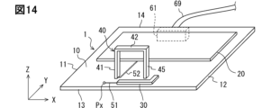
- a connector 61 for connecting a cable 69 may be provided on the edge opposite to the edge where the three-dimensional antenna is formed.
- the three-dimensional antenna may be formed near the edge opposite to the edge where the connector 61 is arranged.
- the three-dimensional antenna may be formed near the third edge 13.
- the vicinity of the third edge 13 may be interpreted as the range from the center of the substrate 10 to the third edge 13.
- the vicinity of the third edge 13 may be interpreted as the range within 15 mm from the third edge 13 in a narrow sense.
- FIG. 14 shows a configuration in which the connector 61 is arranged near the fourth edge 14 of the second surface of the substrate 10.
- the edge where the connector 61 is arranged may be referred to as the connector arrangement edge.
- the fourth edge 14 corresponds to the connector arrangement edge.
- leakage current into the cable 69 can reduce the gain of the three-dimensional antenna.
- the size of the ground plate 20 is smaller than 0.5 ⁇ , performance degradation due to leakage current into the cable 69 is likely to occur.
- antenna performance gain, etc.
- the same characteristics can be obtained even if the roles (connections) of the first element 30 and the second element 40 are swapped. That is, in the antenna device 1, the second element 40 may be connected to the antenna connection terminal of the communication IC, and the first element 30 may be electrically connected to the ground plate 20.
- the relative positions of the components on the substrate 10, in other words the layout, may be changed.
- the first element 30 and the second element 40 may be disposed near the first edge 11, the second edge 12, or the fourth edge 14.
- the base plate 20 may be disposed on the second surface of the substrate 10, and a connector 61, a communication IC, etc. may be disposed on the first surface.
- the first surface of the substrate 10 may be equipped with multiple three-dimensional antennas for diversity.
- the antenna device 1 may have a configuration in which a connector 61 and the like are mounted on the first surface, and a base plate 20 is formed on the second surface.
- the connector 61, power supply circuit 62, communication IC 63, RAM (Random Access Memory) 64, ROM (Read Only Memory) 65, switch 66, first antenna A1, and second antenna A2 are provided on the first surface.
- the connector 61 is provided on the first edge 11. Therefore, in the configuration shown in FIG. 15, the first edge 11 corresponds to the connector arrangement edge.
- the vicinity of the second edge 12 may be utilized as an antenna mounting space.
- the power supply circuit 62, communication IC 63, RAM 64, and ROM 65 may be arranged between the first edge 11, which is the connector arrangement edge, and the center of the substrate 10.
- the first antenna A1 and the second antenna A2 are three-dimensional antennas each including a first element 30 and a second element 40.
- the first antenna A1 and the second antenna A2 are arranged in parallel between the second edge 12 and the center of the substrate 10.
- the first element 30 of the first antenna A1 may have a feeding direction perpendicular to that of the first element 30 of the second antenna A2.
- the feeding direction of the first element 30 of the first antenna A1 is parallel to the X-axis
- the feeding direction of the first element 30 of the second antenna A2 may be parallel to the Y-axis.
- the feeding direction is the direction in which the element extends from the feeding point, in other words, the tangent direction at the feeding point.
- the switch 66 is a switch circuit for switching the antenna connected to the antenna connection terminal of the communication IC 63.
- the switch 66 can be in a first connection state in which the first antenna A1 is connected to the communication IC 63, and a second connection state in which the second antenna A2 is connected to the communication IC 63.
- the connection state of the switch 66 is switched by the communication IC 63.
- the switch 66 may be built into the communication IC 63. In that case, the communication IC 63 may be provided with an antenna connection terminal for each antenna.
- the antenna device 1 may include a third antenna B1, which is a pattern antenna, in addition to the first antenna A1 and second antenna A2 having a three-dimensional structure as shown in FIG. 16.
- the third antenna B1 may be a monopole antenna or a dipole antenna formed along the first surface. While the first antenna A1 and the second antenna A2 are vertically polarized antennas that mainly support vertically polarized waves on the substrate, the third antenna B1 may function as a horizontally polarized antenna that mainly supports parallel polarization on the substrate.
- the above antenna device 1 may be attached to a metal plate at a distance of ⁇ /6 (approximately 20 mm) or more from a corner of the vehicle as shown in FIG. 17. At a location at a distance of ⁇ /6 or more from the corner, a three-dimensional antenna will have a greater amount of radio waves that will be deflected outside the line of sight than a dipole antenna patterned on the surface of a substrate.
- the antenna device 1 may be attached to a rear fender, front fender, door panel, or the like.
- the antenna device 1 may be disposed not only on the side, but also on the back and front.
- the back may include the inside of the back door or rear bumper.
- the front may include the inside of the front bumper, the inside of the front grille, the back of the emblem, etc.
- the antenna device 1 may have three or more vertically polarized antennas.
- the three vertically polarized antennas may all be the above-mentioned three-dimensional antenna including the first element 30 and the second element 40.
- One of the three or more vertically polarized antennas may be a zero-order resonant antenna.
- the zero-order resonant antenna is an antenna having a basic structure of metamaterial.
- the zero-order resonant antenna has an opposing conductor plate, which is a flat metal conductor arranged to face the ground plate 20, and a short-circuiting section that electrically connects the center of the opposing conductor plate to the ground plate.
- the zero-order resonant antenna is an antenna that generates parallel resonance at a frequency according to the capacitance and inductance formed between the ground plate and the patch section and the inductance of the short-circuiting section.
- the zero-order resonant antenna has a mushroom structure.
- the zero-order resonant antenna may be understood as an antenna to which metamaterial technology is applied.
- the zero-order resonant antenna is sometimes called a metamaterial antenna.
- parallel is not limited to a completely parallel state.
- the “parallel” state also includes a state inclined by several degrees to about 15 degrees.
- the expression “parallel” can include a state in which the two are generally parallel (so-called substantially parallel state).
- vertical in the present disclosure is also not limited to a completely vertical state, but also includes a state inclined by several degrees to about 15 degrees.
- “facing” refers to a state in which the two members face each other with a predetermined distance between them.
- the facing state also includes a state in which the two members face each other generally, such as a state in which the two members face each other with a tilt of about 15 degrees.
- the present disclosure also includes the following technical ideas.
- the present disclosure also includes a wireless communication device and a wireless communication system using the following antenna device.
- a substrate (10) which is a plate-shaped dielectric material;
- a ground plane (20) which is a plate-shaped conductor provided on the surface or inside of the substrate;
- a first element (30) which is a linear conductor element provided along the surface of the substrate;
- a second element (40) which is a linear conductor element having a three-dimensional shape;
- the second element is A standing portion (41) perpendicular to the substrate; a substrate parallel portion (42) extending from an upper end of the standing portion so as to be parallel to the substrate, the substrate parallel portion has a portion that is parallel to at least a part of the first element,
- An antenna device wherein one of a lower end of the standing portion and an end of the first element is connected to a feed line, and the other is electrically connected to the ground plane.
- the other end here may be understood to mean either the lower end of the standing portion or the end of the first element, whichever is not connected to the power supply line.
- the substrate parallel portion includes a third end portion that is an end portion connected to the standing portion, and a fourth end portion (45) that is an end portion opposite the third end portion,
- the standing portion is a first standing portion,
- the length of the first element is set to one-fourth of a target wavelength, which is the wavelength of a radio wave to be transmitted or received,
- a target wavelength which is the wavelength of a radio wave to be transmitted or received
- the antenna device according to Technical Idea 4 wherein the length of the second element is set longer than that of the first element.
- the substrate is rectangular and includes four edges; One edge (14) of the four edges is a connector arrangement edge provided with a connector (61) for connecting to a cable; An antenna device described in any one of technical ideas 1 to 6, wherein the first element and the second element are arranged between the edge opposite the connector arrangement edge among the four edges and the center of the substrate.
- the first element has a first end (31) and a second end (32) as ends, The first end is electrically connected to the power supply line or the ground plane, The first end and the lower end are disposed adjacent to each other with a predetermined distance therebetween, The first element extends from the first end in an adjacent direction from the lower end toward the first end,
- the antenna device according to any one of technical ideas 1 to 8, wherein the substrate parallel portion extends from an upper end of the standing portion toward the adjacent direction.
- the first element has a first end (31) and a second end (32) as ends, The first end is electrically connected to the power supply line or the ground plane, The first element has a straight portion extending in a predetermined direction from the first end portion, The lower end of the second element is disposed adjacent to the first end,
- the antenna device according to any one of Technical Ideas 1 to 8, wherein the substrate parallel portion extends from an upper end of the standing portion toward the predetermined direction.
- An antenna device described in any one of technical ideas 1 to 10 which is attached to a metal part of a vehicle body that is at least one-sixth of the target wavelength, which is the wavelength of the radio waves to be transmitted or received, from a corner part of the vehicle.
Landscapes
- Engineering & Computer Science (AREA)
- Remote Sensing (AREA)
- Details Of Aerials (AREA)
- Variable-Direction Aerials And Aerial Arrays (AREA)
- Support Of Aerials (AREA)
Priority Applications (1)
| Application Number | Priority Date | Filing Date | Title |
|---|---|---|---|
| US19/358,109 US20260039013A1 (en) | 2023-04-24 | 2025-10-14 | Antenna device |
Applications Claiming Priority (2)
| Application Number | Priority Date | Filing Date | Title |
|---|---|---|---|
| JP2023071011A JP2024156499A (ja) | 2023-04-24 | 2023-04-24 | アンテナ装置 |
| JP2023-071011 | 2023-04-24 |
Related Child Applications (1)
| Application Number | Title | Priority Date | Filing Date |
|---|---|---|---|
| US19/358,109 Continuation US20260039013A1 (en) | 2023-04-24 | 2025-10-14 | Antenna device |
Publications (1)
| Publication Number | Publication Date |
|---|---|
| WO2024224923A1 true WO2024224923A1 (ja) | 2024-10-31 |
Family
ID=93256218
Family Applications (1)
| Application Number | Title | Priority Date | Filing Date |
|---|---|---|---|
| PCT/JP2024/012212 Ceased WO2024224923A1 (ja) | 2023-04-24 | 2024-03-27 | アンテナ装置 |
Country Status (3)
| Country | Link |
|---|---|
| US (1) | US20260039013A1 (https=) |
| JP (1) | JP2024156499A (https=) |
| WO (1) | WO2024224923A1 (https=) |
Citations (3)
| Publication number | Priority date | Publication date | Assignee | Title |
|---|---|---|---|---|
| JP2012249004A (ja) * | 2011-05-26 | 2012-12-13 | Toyota Central R&D Labs Inc | 広角指向性アンテナ |
| US20200328522A1 (en) * | 2019-04-11 | 2020-10-15 | International Business Machines Corporation | Compact dipole antenna design |
| JP2023002321A (ja) * | 2021-06-22 | 2023-01-10 | 株式会社Soken | 車両用無線装置 |
-
2023
- 2023-04-24 JP JP2023071011A patent/JP2024156499A/ja active Pending
-
2024
- 2024-03-27 WO PCT/JP2024/012212 patent/WO2024224923A1/ja not_active Ceased
-
2025
- 2025-10-14 US US19/358,109 patent/US20260039013A1/en active Pending
Patent Citations (3)
| Publication number | Priority date | Publication date | Assignee | Title |
|---|---|---|---|---|
| JP2012249004A (ja) * | 2011-05-26 | 2012-12-13 | Toyota Central R&D Labs Inc | 広角指向性アンテナ |
| US20200328522A1 (en) * | 2019-04-11 | 2020-10-15 | International Business Machines Corporation | Compact dipole antenna design |
| JP2023002321A (ja) * | 2021-06-22 | 2023-01-10 | 株式会社Soken | 車両用無線装置 |
Also Published As
| Publication number | Publication date |
|---|---|
| JP2024156499A (ja) | 2024-11-06 |
| US20260039013A1 (en) | 2026-02-05 |
Similar Documents
| Publication | Publication Date | Title |
|---|---|---|
| US8299971B2 (en) | Control module chassis-integrated slot antenna | |
| US20240006741A1 (en) | Resonant Cavity Antenna and Electronic Device | |
| JP5482171B2 (ja) | アンテナ装置、及び無線端末装置 | |
| CN118160151B (zh) | 天线单元、天线及天馈系统 | |
| TWI723744B (zh) | 行動裝置與天線結構 | |
| US12531344B2 (en) | Antenna device and communication device | |
| US20240088573A1 (en) | Vehicle wireless device | |
| US8358252B2 (en) | Antenna | |
| EP3091608B1 (en) | Antenna system and antenna module with a parasitic element for radiation pattern improvements | |
| CN100468865C (zh) | 复合天线 | |
| WO2024224923A1 (ja) | アンテナ装置 | |
| US12347945B2 (en) | Wireless communication device | |
| CN113140889B (zh) | 移动装置 | |
| JP7790362B2 (ja) | アンテナ装置 | |
| WO2022038995A1 (ja) | アンテナ装置 | |
| CN118610725B (zh) | 天线、天线系统和汽车 | |
| CN119231167B (zh) | 天线组件及电子设备 | |
| CN218448448U (zh) | 一种宽带Sub-6GHz天线 | |
| US12261379B2 (en) | Antenna device | |
| JP2007336279A (ja) | アンテナ | |
| CN119070031A (zh) | 电子设备 | |
| CN118676585A (zh) | 天线组件及电子设备 | |
| CN121529184A (zh) | 天线结构、射频装置、雷达传感器与超宽带装置 | |
| CN121011835A (zh) | 天线装置以及电子设备 |
Legal Events
| Date | Code | Title | Description |
|---|---|---|---|
| 121 | Ep: the epo has been informed by wipo that ep was designated in this application |
Ref document number: 24796681 Country of ref document: EP Kind code of ref document: A1 |
|
| NENP | Non-entry into the national phase |
Ref country code: DE |