WO2024219258A1 - 検出装置 - Google Patents
検出装置 Download PDFInfo
- Publication number
- WO2024219258A1 WO2024219258A1 PCT/JP2024/014073 JP2024014073W WO2024219258A1 WO 2024219258 A1 WO2024219258 A1 WO 2024219258A1 JP 2024014073 W JP2024014073 W JP 2024014073W WO 2024219258 A1 WO2024219258 A1 WO 2024219258A1
- Authority
- WO
- WIPO (PCT)
- Prior art keywords
- light source
- photodiode
- detection
- mode
- readout
- Prior art date
- Legal status (The legal status is an assumption and is not a legal conclusion. Google has not performed a legal analysis and makes no representation as to the accuracy of the status listed.)
- Ceased
Links
Images





Classifications
-
- G—PHYSICS
- G06—COMPUTING OR CALCULATING; COUNTING
- G06V—IMAGE OR VIDEO RECOGNITION OR UNDERSTANDING
- G06V40/00—Recognition of biometric, human-related or animal-related patterns in image or video data
- G06V40/10—Human or animal bodies, e.g. vehicle occupants or pedestrians; Body parts, e.g. hands
- G06V40/12—Fingerprints or palmprints
- G06V40/13—Sensors therefor
- G06V40/1318—Sensors therefor using electro-optical elements or layers, e.g. electroluminescent sensing
-
- A—HUMAN NECESSITIES
- A61—MEDICAL OR VETERINARY SCIENCE; HYGIENE
- A61B—DIAGNOSIS; SURGERY; IDENTIFICATION
- A61B5/00—Measuring for diagnostic purposes; Identification of persons
- A61B5/02—Detecting, measuring or recording for evaluating the cardiovascular system, e.g. pulse, heart rate, blood pressure or blood flow
-
- A—HUMAN NECESSITIES
- A61—MEDICAL OR VETERINARY SCIENCE; HYGIENE
- A61B—DIAGNOSIS; SURGERY; IDENTIFICATION
- A61B5/00—Measuring for diagnostic purposes; Identification of persons
- A61B5/02—Detecting, measuring or recording for evaluating the cardiovascular system, e.g. pulse, heart rate, blood pressure or blood flow
- A61B5/024—Measuring pulse rate or heart rate
- A61B5/02416—Measuring pulse rate or heart rate using photoplethysmograph signals, e.g. generated by infrared radiation
- A61B5/02427—Details of sensor
- A61B5/02433—Details of sensor for infrared radiation
-
- A—HUMAN NECESSITIES
- A61—MEDICAL OR VETERINARY SCIENCE; HYGIENE
- A61B—DIAGNOSIS; SURGERY; IDENTIFICATION
- A61B5/00—Measuring for diagnostic purposes; Identification of persons
- A61B5/117—Identification of persons
- A61B5/1171—Identification of persons based on the shapes or appearances of their bodies or parts thereof
-
- A—HUMAN NECESSITIES
- A61—MEDICAL OR VETERINARY SCIENCE; HYGIENE
- A61B—DIAGNOSIS; SURGERY; IDENTIFICATION
- A61B5/00—Measuring for diagnostic purposes; Identification of persons
- A61B5/117—Identification of persons
- A61B5/1171—Identification of persons based on the shapes or appearances of their bodies or parts thereof
- A61B5/1172—Identification of persons based on the shapes or appearances of their bodies or parts thereof using fingerprinting
-
- A—HUMAN NECESSITIES
- A61—MEDICAL OR VETERINARY SCIENCE; HYGIENE
- A61B—DIAGNOSIS; SURGERY; IDENTIFICATION
- A61B5/00—Measuring for diagnostic purposes; Identification of persons
- A61B5/145—Measuring characteristics of blood in vivo, e.g. gas concentration or pH-value ; Measuring characteristics of body fluids or tissues, e.g. interstitial fluid or cerebral tissue
- A61B5/1455—Measuring characteristics of blood in vivo, e.g. gas concentration or pH-value ; Measuring characteristics of body fluids or tissues, e.g. interstitial fluid or cerebral tissue using optical sensors, e.g. spectral photometrical oximeters
-
- A—HUMAN NECESSITIES
- A61—MEDICAL OR VETERINARY SCIENCE; HYGIENE
- A61B—DIAGNOSIS; SURGERY; IDENTIFICATION
- A61B5/00—Measuring for diagnostic purposes; Identification of persons
- A61B5/145—Measuring characteristics of blood in vivo, e.g. gas concentration or pH-value ; Measuring characteristics of body fluids or tissues, e.g. interstitial fluid or cerebral tissue
- A61B5/1455—Measuring characteristics of blood in vivo, e.g. gas concentration or pH-value ; Measuring characteristics of body fluids or tissues, e.g. interstitial fluid or cerebral tissue using optical sensors, e.g. spectral photometrical oximeters
- A61B5/14551—Measuring characteristics of blood in vivo, e.g. gas concentration or pH-value ; Measuring characteristics of body fluids or tissues, e.g. interstitial fluid or cerebral tissue using optical sensors, e.g. spectral photometrical oximeters for measuring blood gases
- A61B5/14552—Details of sensors specially adapted therefor
-
- G—PHYSICS
- G06—COMPUTING OR CALCULATING; COUNTING
- G06T—IMAGE DATA PROCESSING OR GENERATION, IN GENERAL
- G06T1/00—General purpose image data processing
-
- G—PHYSICS
- G06—COMPUTING OR CALCULATING; COUNTING
- G06V—IMAGE OR VIDEO RECOGNITION OR UNDERSTANDING
- G06V10/00—Arrangements for image or video recognition or understanding
- G06V10/10—Image acquisition
- G06V10/12—Details of acquisition arrangements; Constructional details thereof
- G06V10/14—Optical characteristics of the device performing the acquisition or on the illumination arrangements
- G06V10/141—Control of illumination
-
- H—ELECTRICITY
- H10—SEMICONDUCTOR DEVICES; ELECTRIC SOLID-STATE DEVICES NOT OTHERWISE PROVIDED FOR
- H10F—INORGANIC SEMICONDUCTOR DEVICES SENSITIVE TO INFRARED RADIATION, LIGHT, ELECTROMAGNETIC RADIATION OF SHORTER WAVELENGTH OR CORPUSCULAR RADIATION
- H10F39/00—Integrated devices, or assemblies of multiple devices, comprising at least one element covered by group H10F30/00, e.g. radiation detectors comprising photodiode arrays
- H10F39/10—Integrated devices
- H10F39/12—Image sensors
-
- H—ELECTRICITY
- H10—SEMICONDUCTOR DEVICES; ELECTRIC SOLID-STATE DEVICES NOT OTHERWISE PROVIDED FOR
- H10F—INORGANIC SEMICONDUCTOR DEVICES SENSITIVE TO INFRARED RADIATION, LIGHT, ELECTROMAGNETIC RADIATION OF SHORTER WAVELENGTH OR CORPUSCULAR RADIATION
- H10F55/00—Radiation-sensitive semiconductor devices covered by groups H10F10/00, H10F19/00 or H10F30/00 being structurally associated with electric light sources and electrically or optically coupled thereto
-
- H—ELECTRICITY
- H10—SEMICONDUCTOR DEVICES; ELECTRIC SOLID-STATE DEVICES NOT OTHERWISE PROVIDED FOR
- H10K—ORGANIC ELECTRIC SOLID-STATE DEVICES
- H10K30/00—Organic devices sensitive to infrared radiation, light, electromagnetic radiation of shorter wavelength or corpuscular radiation
- H10K30/30—Organic devices sensitive to infrared radiation, light, electromagnetic radiation of shorter wavelength or corpuscular radiation comprising bulk heterojunctions, e.g. interpenetrating networks of donor and acceptor material domains
-
- H—ELECTRICITY
- H10—SEMICONDUCTOR DEVICES; ELECTRIC SOLID-STATE DEVICES NOT OTHERWISE PROVIDED FOR
- H10K—ORGANIC ELECTRIC SOLID-STATE DEVICES
- H10K39/00—Integrated devices, or assemblies of multiple devices, comprising at least one organic radiation-sensitive element covered by group H10K30/00
- H10K39/30—Devices controlled by radiation
-
- H—ELECTRICITY
- H10—SEMICONDUCTOR DEVICES; ELECTRIC SOLID-STATE DEVICES NOT OTHERWISE PROVIDED FOR
- H10F—INORGANIC SEMICONDUCTOR DEVICES SENSITIVE TO INFRARED RADIATION, LIGHT, ELECTROMAGNETIC RADIATION OF SHORTER WAVELENGTH OR CORPUSCULAR RADIATION
- H10F77/00—Constructional details of devices covered by this subclass
- H10F77/20—Electrodes
- H10F77/244—Electrodes made of transparent conductive layers, e.g. transparent conductive oxide [TCO] layers
- H10F77/247—Electrodes made of transparent conductive layers, e.g. transparent conductive oxide [TCO] layers comprising indium tin oxide [ITO]
Definitions
- the present invention relates to a detection device.
- Optical sensors capable of detecting fingerprint patterns and vein patterns are known (for example, see Patent Document 1). Such optical sensors have multiple photodiodes that use an organic semiconductor material as the active layer. As described in Patent Document 2, the photodiodes are disposed between a lower electrode and an upper electrode, and are stacked, for example, in the order of the lower electrode, electron transport layer, active layer, hole transport layer, and upper electrode.
- a single optical sensor may be used to measure various types of biometric information, such as blood oxygen saturation (hereinafter referred to as blood oxygen saturation (SpO2)) and imaging of vascular patterns such as veins.
- Optical sensors are required to improve their detection accuracy when measuring different objects and different types of biometric information.
- the present invention aims to provide a detection device that can improve detection accuracy.
- a detection device includes a photodiode stacked in the order of a lower electrode, a lower buffer layer, an active layer, an upper buffer layer, and an upper electrode; a first light source and a second light source that irradiate the photodiode with light; a light source drive circuit that controls the lighting of the first light source and the second light source; and a detection circuit that is connected to the photodiode and outputs a sensor value corresponding to the photocurrent output from the photodiode.
- the detection circuit measures an integrated value of the photocurrent in each of a plurality of readout periods
- the light source drive circuit has a first mode in which the first light source and the second light source are alternately turned on in the plurality of readout periods, and a second mode in which either the first light source or the second light source is turned on in the plurality of readout periods.
- the readout period of the detection circuit includes a first readout period in the first mode, and a second readout period in the second mode that has a period different from the first readout period.
- FIG. 1 is a plan view illustrating a detection device according to an embodiment.
- FIG. 2 is a cross-sectional view taken along line II-II' of FIG.
- FIG. 3 is a block diagram illustrating an example of the configuration of the detection device according to the embodiment.
- FIG. 4 is a circuit diagram illustrating an example of the configuration of a detection device according to an embodiment.
- FIG. 5 is a timing waveform diagram showing an example of operation of the detection device according to the embodiment in the first mode.
- FIG. 6 is a timing waveform diagram showing an example of the operation of the detection device according to the embodiment in the second mode.
- FIG. 7 is a graph for explaining the response characteristics of a photodiode.
- FIG. 8 is a graph showing an enlarged view of a portion of the first region and the second region in FIG.
- the term "on top” is used, unless otherwise specified, to include both a case in which another structure is placed directly on top of a structure so as to be in contact with the structure, and a case in which another structure is placed above a structure via yet another structure.
- (Embodiment) 1 is a plan view showing a schematic configuration of a detection device according to an embodiment of the present invention, the detection device 1 includes a substrate 21, a plurality of photodiodes PD, a plurality of signal lines SL, a plurality of shield layers 26, power supply lines CL1, CL2, and CL3, and a control circuit 122.
- the substrate 21 has a detection area AA and a peripheral area GA.
- the detection area AA is an area in which multiple photodiodes PD are provided.
- the peripheral area GA is an area between the outer periphery of the detection area AA and the edge of the substrate 21, and is an area in which multiple photodiodes PD are not provided.
- Multiple signal lines SL and a control circuit 122 are provided in the peripheral area GA of the substrate 21.
- the first direction Dx is a direction in a plane parallel to the substrate 21.
- the second direction Dy is a direction in a plane parallel to the substrate 21, and is a direction perpendicular to the first direction Dx.
- the second direction Dy may intersect the first direction Dx without being perpendicular to it.
- the third direction Dz is a direction perpendicular to the first direction Dx and the second direction Dy.
- the third direction Dz is the normal direction of the substrate 21.
- plane view refers to the positional relationship when viewed from a direction perpendicular to the substrate 21.
- the detection device 1 has multiple photodiodes PD as light sensor elements. Each photodiode PD outputs an electrical signal according to the light irradiated thereon. More specifically, the photodiode PD is an OPD (Organic Photodiode) that uses an organic semiconductor. The multiple photodiodes PD are arranged side by side in the second direction Dy in the detection area AA.
- OPD Organic Photodiode
- the photodiodes PD include an organic semiconductor layer 30 (lower buffer layer 32, active layer 31, upper buffer layer 33 (see FIG. 2)), a lower electrode 23 arranged at the lower part of the organic semiconductor layer 30, and an upper electrode 24 arranged at the upper part of the organic semiconductor layer 30.
- the lower electrodes 23 are provided for each of the photodiodes PD, and are arranged in the detection area AA in the second direction Dy.
- the lower electrodes 23 are also arranged at a distance from each other in the second direction Dy.
- the organic semiconductor layer 30 and the upper electrode 24 are provided across the photodiodes PD, and are provided continuously in the detection area AA. In FIG.
- the organic semiconductor layer 30 and the upper electrode 24 provided above the lower electrode 23 are represented by dashed lines and two-dot chain lines, respectively.
- the stacked configuration of the photodiodes PD, the lower electrodes 23, and the upper electrodes 24 will be described later with reference to FIG. 2.
- the multiple signal lines SL are electrically connected to each of the lower electrodes 23 of the multiple photodiodes PD. Specifically, in the example shown in FIG. 1, the multiple signal lines SL are connected to each of the multiple lower electrodes 23 via contact holes CH1 formed in the insulating film 27 (see FIG. 2).
- Each of the multiple signal lines SL extends in the first direction Dx from the connection point (contact hole CH1) with the lower electrode 23, bends in the second direction Dy, and extends in the second direction Dy along the arrangement direction of the multiple photodiodes PD.
- the portions of the multiple signal lines SL extending in the second direction Dy are arranged in the first direction Dx.
- the multiple signal lines SL are connected to a detection circuit 48 included in the control circuit 122. In other words, the detection circuit 48 is electrically connected to the lower electrodes 23 of the multiple photodiodes PD via the multiple signal lines SL.
- the signal lines SL and shield layers 26 are provided for each of the photodiodes PD.
- the multiple shield layers 26 are arranged to overlap each of the multiple signal lines SL in a planar view. More specifically, the multiple shield layers 26 overlap portions of the multiple signal lines SL that extend in the first direction Dx, and extend in the first direction Dx along the multiple signal lines SL.
- the multiple shield layers 26 each extend across the detection area AA and the peripheral area GA. Furthermore, the multiple shield layers 26 are arranged in the second direction Dy, overlapping each of the multiple signal lines SL.
- the multiple shield layers 26 are connected to the power supply circuit 123 of the control circuit 122 via power supply lines CL1 and CL2 extending in the second direction Dy. More specifically, the power supply line CL1 is provided in the same layer as the multiple shield layers 26 and intersects with the multiple shield layers 26. As a result, the multiple shield layers 26 are bundled and connected to the common power supply line CL1.
- the power supply line CL2 is provided in the same layer as the multiple signal lines SL, and is electrically connected to the power supply line CL1 via a contact hole CH2.
- the power supply line CL2 is also electrically connected to the power supply circuit 123.
- the power supply circuit 123 supplies a reference voltage VCOM to the multiple shield layers 26 via the power supply lines CL1 and CL2.
- the reference voltage VCOM is a voltage signal having a fixed, predetermined potential.
- the reference voltage VCOM is, for example, a voltage signal having a potential equivalent to the reference potential Vref supplied to the lower electrode 23.
- the reference potential Vref is a fixed, predetermined potential.
- the power supply line CL1 is provided adjacent to the organic semiconductor layer 30 in the first direction Dx.
- the connection between the multiple shield layers 26 and the power supply circuit 123 may be in any configuration, and the arrangement and number of the power supply lines CL1 and CL2 can be changed as appropriate.
- the upper electrode 24 is provided to extend in the second direction Dy across the detection area AA and the peripheral area GA. That is, the upper electrode 24 is provided to extend from the area that overlaps with the organic semiconductor layer 30 to the area that does not overlap with the organic semiconductor layer 30, and is electrically connected to the power supply wiring CL3 in the area that does not overlap with the organic semiconductor layer 30.
- the power supply wiring CL3 is provided in the same layer as the multiple signal lines SL, and is electrically connected to the upper electrode 24 via the contact hole CH3 and the terminal portion 24a.
- the terminal portion 24a is provided in the same layer as the lower electrode 23.
- the upper electrodes 24 of the multiple photodiodes PD are connected to the power supply circuit 123 of the control circuit 122 via the terminal portion 24a and the power supply wiring CL3.
- the power supply circuit 123 supplies a reference potential VDD_ORG (see FIG. 3) to the upper electrodes 24 of the photodiodes PD.
- the reference potential VDD_ORG is a fixed, predetermined potential.
- the control circuit 122 (detection circuit 48 and power supply circuit 123) is disposed adjacent to the photodiode PD in the second direction Dy in the peripheral area GA of the substrate 21.
- the control circuit 122 is a circuit that supplies control signals to the multiple photodiodes PD to control the detection operation.
- the multiple photodiodes PD each output an electrical signal corresponding to the light irradiated thereon as a detection signal Vdet to the detection circuit 48. In this way, the detection device 1 detects information about the object to be detected based on the detection signals Vdet from the multiple photodiodes PD.
- control circuit 122 (detection circuit 48 and power supply circuit 123) is provided on the same substrate 21 as the multiple photodiodes PD, but is not limited to this.
- the control circuit 122 (detection circuit 48 and power supply circuit 123) may be provided on a separate control substrate connected to the substrate 21 via, for example, a flexible printed circuit board or the like.
- the detection circuit 48 and the power supply circuit 123 may each be formed as separate circuits.
- the detection device 1 has a first light source 61 and a second light source 62 (see FIG. 3).
- the first light source 61 and the second light source 62 are, for example, inorganic LEDs (Light Emitting Diodes) or organic ELs (OLEDs: Organic Light Emitting Diodes).
- the first light source 61 and the second light source 62 emit light of different wavelengths.
- the first light source 61 emits near-infrared light or infrared light.
- the second light source 62 emits green light or red light.
- the green light has a wavelength of, for example, 490 nm or more and 550 nm or less.
- the red light has a wavelength of, for example, 640 nm or more and 770 nm or less.
- the infrared light has a wavelength of, for example, about 2500 nm or more and about 25 ⁇ m or less.
- Near-infrared light has a wavelength of, for example, about 770 nm or more and about 2500 nm or less.
- the light emitted from the first light source 61 and the second light source 62 is reflected by the surface of the object to be detected, such as a finger, and enters the multiple photodiodes PD.
- the light emitted from the first light source 61 and the second light source 62 may be reflected inside the finger or pass through the finger and enter the multiple photodiodes PD.
- Information about a living body includes, for example, the pulse waves, pulse, and blood vessel images of the finger or palm.
- the detection device 1 may be configured as a fingerprint detection device that detects fingerprints, or a vein detection device that detects blood vessel patterns such as veins.
- the detection device 1 of this embodiment can detect information about a living body, such as pulse waves, pulse rates, and blood vessel images, as well as oxygen saturation in blood (hereinafter referred to as blood oxygen saturation ( SpO2 )), based on the light emitted from the first light source 61 and the light emitted from the second light source 62.
- the detection device 1 has the first light source 61 and the second light source 62, and can detect various pieces of information about a living body by performing detection based on light of different wavelengths emitted from each of them.
- the emission colors of the first light source 61 and the second light source 62 described above are merely examples, and the present disclosure is not limited to the emission colors of the first light source 61 and the second light source 62.
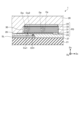
- Figure 2 is a cross-sectional view taken along line II-II' in Figure 1.
- the direction perpendicular to the surface of the substrate 21, from the substrate 21 toward the sealing film 28, is referred to as the "upper side” or simply “upper”.
- the direction from the sealing film 28 toward the substrate 21 is referred to as the "lower side” or simply “lower”.
- the substrate 21 is an insulating substrate, and is made of, for example, glass or a resin material.
- the substrate 21 is not limited to being flat, and may have a curved surface. In this case, the substrate 21 may be a film-like resin.
- the signal line SL is provided on the substrate 21.
- the signal line SL is formed, for example, of a metal wiring, and is formed of a material having better conductivity than the lower electrode 23 of the photodiode PD.
- a part of the signal line SL (the right end side of the signal line SL in FIG. 2) is provided in a layer between the substrate 21 and the photodiode PD in the third direction Dz.
- the insulating film 27 is provided on the substrate 21, covering the signal line SL.
- the insulating film 27 may be an inorganic insulating film or an organic insulating film.
- the insulating film 27 may be a single layer or a laminated film.
- the photodiode PD is provided on the insulating film 27. More specifically, the photodiode PD has a lower electrode 23, a lower buffer layer 32, an active layer 31, an upper buffer layer 33, and an upper electrode 24. The photodiode PD is stacked in the direction perpendicular to the substrate 21 in the following order: lower electrode 23, lower buffer layer 32, active layer 31, upper buffer layer 33, and upper electrode 24.
- the lower electrode 23 is provided on the insulating film 27 and is electrically connected to the signal line SL via a contact hole CH1 provided in the insulating film 27.
- the lower electrode 23 is the cathode electrode of the photodiode PD and is formed of a conductive material having translucency, such as ITO (Indium Tin Oxide).
- the detection device 1 of this embodiment is formed as a bottom-receiving type optical sensor in which light from the object to be detected passes through the substrate 21 and enters the photodiode PD.
- the present invention is not limited to this, and the detection device 1 may also be a top-receiving type optical sensor.
- the characteristics (for example, voltage-current characteristics and resistance value) of the active layer 31 change depending on the light irradiated.
- An organic material is used as the material of the active layer 31.
- the active layer 31 has a bulk heterostructure in which a p-type organic semiconductor and an n-type fullerene derivative (PCBM) which is an n-type organic semiconductor are mixed.
- PCBM n-type fullerene derivative
- low molecular weight organic materials such as C 60 (fullerene), PCBM (phenyl C 61 -butyric acid methyl ester), CuPc (copper phthalocyanine), F 16 CuPc (fluorinated copper phthalocyanine), rubrene (5,6,11,12-tetraphenyltetracene), and PDI (perylene derivative) can be used as the active layer 31.
- C 60 fulllerene
- PCBM phenyl C 61 -butyric acid methyl ester
- CuPc copper phthalocyanine
- F 16 CuPc fluorinated copper phthalocyanine
- rubrene 5,6,11,12-tetraphenyltetracene
- PDI perylene derivative
- the active layer 31 can be formed by a deposition type (dry process) using these low molecular weight organic materials.
- the active layer 31 may be, for example, a laminated film of CuPc and F 16 CuPc, or a laminated film of rubrene and C 60.
- the active layer 31 can also be formed by a coating type (wet process).
- the active layer 31 is made of a material that combines the above-mentioned low molecular weight organic material and a polymer organic material.
- the polymer organic material for example, P3HT (poly(3-hexylthiophene)), F8BT (F8-alt-benzothiadiazole), etc. can be used.
- the active layer 31 can be a film in a state where P3HT and PCBM are mixed, or a film in a state where F8BT and PDI are mixed.
- the lower buffer layer 32 is an electron transport layer
- the upper buffer layer 33 is a hole transport layer.
- the lower buffer layer 32 and the upper buffer layer 33 are provided to facilitate the holes and electrons generated in the active layer 31 reaching the lower electrode 23 or the upper electrode 24.
- the lower buffer layer 32 is in direct contact with the lower electrode 23, and is also provided in the region between adjacent lower electrodes 23.
- the active layer 31 is in direct contact with the lower buffer layer 32.
- the upper buffer layer 33 is in direct contact with the active layer 31, and the upper electrode 24 is in direct contact with the upper buffer layer 33.
- the material of the electron transport layer is ethoxylated polyethyleneimine (PEIE), and the material of the hole transport layer is a metal oxide layer, such as tungsten oxide (WO 3 ) or molybdenum oxide.
- PEIE ethoxylated polyethyleneimine
- WO 3 tungsten oxide
- molybdenum oxide tungsten oxide
- the materials and manufacturing methods of the lower buffer layer 32, the active layer 31, and the upper buffer layer 33 are merely examples, and other materials and manufacturing methods may be used.
- the lower buffer layer 32 and the upper buffer layer 33 are not limited to single-layer films, and may be formed as a laminated film including an electron blocking layer and a hole blocking layer.
- the upper electrode 24 is provided on the upper buffer layer 33.
- the upper electrode 24 is an anode electrode of the photodiode PD, and is formed continuously over the entire detection area AA. In other words, the upper electrode 24 is provided continuously over the multiple photodiodes PD.
- the upper electrode 24 faces the multiple lower electrodes 23, sandwiching the lower buffer layer 32, the active layer 31, and the upper buffer layer 33 therebetween.
- the upper electrode 24 is formed of a conductive material having translucency, such as ITO or IZO.
- the sealing film 28 is provided on the upper electrode 24.
- an inorganic film such as a silicon nitride film or an aluminum oxide film, or a resin film such as acrylic is used.
- the sealing film 28 is not limited to a single layer, and may be a laminated film of two or more layers combining the inorganic film and the resin film.
- the sealing film 28 provides a good seal for the photodiode PD, and can prevent moisture from entering from the upper surface side.
- the shield layer 26 is provided on the insulating film 27 in the same layer as the lower electrode 23.
- the shield layer 26 is formed of the same material as the lower electrode 23, for example, a conductive material having translucency such as ITO.
- the shield layer 26 may be formed of a material different from that of the lower electrode 23, for example, a metal material.
- the shield layer 26 is disposed with a gap between it and the lower electrode 23 in the first direction Dx.
- the shield layer 26 also faces the signal line SL in the third direction Dz via the insulating film 27.
- a part of the shield layer 26 is disposed between the signal line SL and the lower buffer layer 32 of the photodiode PD in the third direction Dz.
- the organic semiconductor layer 30 (the lower buffer layer 32, the active layer 31 and the upper buffer layer 33) is provided to cover the lower electrode 23 and to cover a part of the shield layer 26.
- the multiple shield layers 26 are supplied with a reference voltage VCOM. As a result, the shield layers 26 suppress the parasitic capacitance between the upper electrode 24 of the photodiode PD and the signal line SL, and suppress unintended capacitive coupling between the photodiode PD (upper electrode 24) and the signal line SL.
- the detection device 1 of this embodiment may be configured without the shield layer 26.
- the lower electrode 23 is a cathode electrode and the upper electrode 24 is an anode electrode
- the lower electrode 23 may be an anode electrode and the upper electrode 24 may be a cathode electrode.
- the lower buffer layer 32 may be a hole transport layer
- the upper buffer layer 33 may be an electron transport layer.
- FIG. 3 is a block diagram showing an example of the configuration of the detection device according to the embodiment.
- the control circuit 122 includes a detection circuit 48, a power supply circuit 123, a light source drive circuit 124, a mode switching circuit 125, a timing control circuit 126, and a memory circuit 127.
- the detection circuit 48 is a current detection circuit that measures the current (photocurrent Ip) output from the photodiode PD.
- the detection circuit 48 is configured to include, for example, an operational amplifier circuit 42 and an A/D conversion circuit 43 (see FIG. 4).
- the detection circuit 48 measures the photocurrent Ip output from the photodiode PD, performs signal processing such as A/D conversion, and outputs a sensor value So corresponding to the photocurrent Ip to the host IC 101.
- the power supply circuit 123 supplies a reference potential VDD_ORG to the anode of the photodiode PD, and also supplies a reference potential Vref to the cathode of the photodiode PD.
- the reference potential Vref has a higher potential than the reference potential VDD_ORG. This causes the photodiode PD to be reverse bias driven.
- the light source drive circuit 124 supplies a light source control signal LED1 to the first light source 61, and supplies a light source control signal LED2 to the second light source 62. In this way, the light source drive circuit 124 controls the lighting and non-lighting of each of the first light source 61 and the second light source 62. The first light source 61 and the second light source 62 irradiate light to the photodiode PD based on the light source control signals LED1 and LED2 from the light source drive circuit 124.
- the mode switching circuit 125 is a circuit that switches between a detection operation in a first mode M1 and a detection operation in a second mode M2 based on a mode selection signal SEL from the host IC 101.
- the first mode M1 and the second mode M2 are detection modes that are preset to correspond to the detection of different biological information or the detection of different detectable objects, respectively.
- the detection device 1 detects blood oxygen saturation ( SpO2 ) in the first mode M1 and detects (images) a vein pattern in the second mode M2.
- SpO2 blood oxygen saturation
- the detection circuit 48 changes the length of the readout period RD of each of the first mode M1 and the second mode M2 based on the mode switching control signal from the mode switching circuit 125.
- the light source drive circuit 124 switches the lighting pattern of the first light source 61 and the second light source 62 based on the mode switching control signal from the mode switching circuit 125.
- the timing control circuit 126 controls each circuit in the control circuit 122 to operate synchronously or asynchronously.
- the memory circuit 127 temporarily stores the sensor value So detected in the first mode M1 and the sensor value So detected in the second mode M2.
- the memory circuit 127 also stores in advance various information such as information regarding the length of the readout period RD of each of the first mode M1 and the second mode M2, and the lighting patterns of the first light source 61 and the second light source 62.
- FIG. 4 is a circuit diagram showing an example of the configuration of a detection device according to an embodiment. Note that FIG. 4 shows a schematic diagram of one photodiode PD out of the multiple photodiodes PD (see FIG. 1).
- the anode of the photodiode PD is supplied with a reference potential VDD_ORG from the power supply circuit 123 (see FIG. 1).
- the cathode of the photodiode PD is connected to the detection circuit 48. More specifically, the cathode of the photodiode PD is connected to the inverting input (-) of the operational amplifier circuit 42 via the connection switch SSW.
- the sensor capacitance Cs is connected in parallel to the photodiode PD.
- the sensor capacitance Cs is a capacitance formed between the upper electrode 24 and the lower electrode 23 of the photodiode PD.
- the detection circuit 48 includes an operational amplifier circuit 42, an A/D conversion circuit 43, a connection switch SSW, and a reset switch RSW.
- the operational amplifier circuit 42 converts fluctuations in the photocurrent Ip output from the photodiode PD into voltage fluctuations.
- the A/D conversion circuit 43 converts the analog signal output from the operational amplifier circuit 42 into a digital signal.
- the connection switch SSW switches between on (connection) and off (disconnection) between the operational amplifier circuit 42 and the photodiode PD.
- the reset switch RSW is provided to reset the charge of the capacitance element Cf of the operational amplifier circuit 42 during the reset period.
- a reference potential Vref having a fixed potential is input to the non-inverting input (+) of the operational amplifier circuit 42.
- the connection switch SSW is turned on during the readout period RD, the photodiode PD is connected to the inverting input (-) of the operational amplifier circuit 42. Due to an imaginary short of the operational amplifier circuit 42, the cathode of the photodiode PD is at the same reference potential Vref as the non-inverting input (+).
- the reference potential Vref has a higher potential than the reference potential VDD_ORG. As a result, the photodiode PD is reverse bias driven.
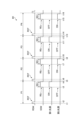
- Fig. 5 is a timing waveform diagram showing an example of the operation of the detection device according to the embodiment in the first mode.
- Fig. 6 is a timing waveform diagram showing an example of the operation of the detection device according to the embodiment in the second mode.
- the detection device 1 has detection periods P1, P2, P3, and P4 in the first mode M1.
- the detection device 1 has a reset period during which the reset switch RSW is on, and a first readout period RD1 during which the connection switch SSW is on.
- the exposure period during which light is irradiated from the first light source 61 or the second light source 62 to the photodiode PD overlaps with the first readout period RD1.
- detection period P when there is no need to distinguish between detection periods P1, P2, P3, and P4, they may simply be referred to as detection period P.
- the light source drive circuit 124 controls the lighting and non-lighting of the first light source 61 and the second light source 62 for each detection period P1, P2, P3, and P4. In the first mode M1, the light source drive circuit 124 alternately lights the first light source 61 and the second light source 62 for the detection periods P1, P2, P3, and P4 (multiple first readout periods RD1).
- the first light source 61 is turned on and the second light source 62 is turned off.
- the first light source 61 is turned off and the second light source 62 is turned on.
- the first readout period RD1 of the detection period P3 the first light source 61 is turned on and the second light source 62 is turned off.
- the first light source 61 is turned off and the second light source 62 is turned on.
- the detection circuit 48 measures the photocurrent Ip(NIR) output from the photodiode PD in response to the light irradiated from the first light source 61 during the first readout period RD1 of the detection periods P1 and P3.
- the detection circuit 48 also measures the photocurrent Ip(R) output from the photodiode PD in response to the light irradiated from the second light source 62 during the first readout period RD1 of the detection periods P2 and P4.
- photocurrent Ip(NIR) is the current component of photocurrent Ip that is output from photodiode PD in response to light (e.g., near-infrared light) emitted from first light source 61.
- Photocurrent Ip(R) is the current component of photocurrent Ip that is output from photodiode PD in response to light (e.g., red light) emitted from second light source 62.
- the detection circuit 48 outputs a sensor value So corresponding to the photocurrent Ip output from the photodiode PD during each of the first readout periods RD1 of the detection periods P1, P2, P3, and P4 that are provided in a time-division manner.
- the detection period P1 starts at time t1.
- the reset switch RSW is on (connected state) based on the reset control signal RST from the mode switching circuit 125. This resets the charge of the capacitance element Cf of the operational amplifier circuit 42.
- the reset switch RSW is off (disconnected state) and the reset period ends.
- connection switch SSW is on (connected state) based on the read control signal REx from the mode switching circuit 125. This causes the detection circuit 48 to start the first read period RD1 of the detection period P1. More specifically, at time t3, the operational amplifier circuit 42 of the detection circuit 48 is connected to the cathode of the photodiode PD via the connection switch SSW. Also, at time t3, based on the light source control signals LED1 and LED2 from the light source drive circuit 124, the first light source 61 is turned on and the second light source 62 is turned off.
- the photodiode PD outputs a photocurrent Ip(NIR) in response to the light from the first light source 61.
- the detection circuit 48 measures the integrated value of the photocurrent Ip(NIR). Then, the detection circuit 48 outputs a sensor value So(NIR) corresponding to the integrated value of the photocurrent Ip(NIR) to the host IC 101.
- the connection switch SSW is off (disconnected state) based on the read control signal REx from the mode switching circuit 125. This causes the detection circuit 48 to end the first read period RD1 of the detection period P1. In this way, the mode switching circuit 125 controls the length of the first read period RD1 in the first mode M1 by turning the connection switch SSW on and off. Also, at time t4, the first light source 61 and the second light source 62 are not lit based on the light source control signals LED1 and LED2 from the light source drive circuit 124.
- the detection period P2 begins.
- the reset switch RSW is on (connected state) based on the reset control signal RST from the mode switching circuit 125. This resets the charge of the capacitance element Cf of the operational amplifier circuit 42.
- the reset switch RSW is off (disconnected state) and the reset period ends.
- connection switch SSW is on (connected state) based on the read control signal REx from the mode switching circuit 125. This causes the detection circuit 48 to start the first read period RD1 of the detection period P2. Also, at time t7, the first light source 61 is not lit and the second light source 62 is lit based on the light source control signals LED1 and LED2 from the light source drive circuit 124.
- the photodiode PD outputs a photocurrent Ip(R) in response to the light from the second light source 62.
- the detection circuit 48 measures the integrated value of the photocurrent Ip(R). Then, the detection circuit 48 outputs a sensor value So(R) corresponding to the integrated value of the photocurrent Ip(R) to the host IC 101.
- connection switch SSW is off (disconnected state) based on the read control signal REx from the mode switching circuit 125. This causes the detection circuit 48 to end the first read period RD1 of the detection period P2. Also, at time t8, the first light source 61 and the second light source 62 are not lit based on the light source control signals LED1 and LED2 from the light source drive circuit 124.
- the detection device 1 then measures the photocurrent Ip during each of the first readout periods RD1 of the detection periods P3 and P4.
- the detection periods P3 and P4 are similar to the detection periods P1 and P2 described above, and a repeated description will be omitted.
- the host IC 101 can calculate blood oxygen saturation (SpO2) using the sensor value So(NIR) obtained by the first light (near-infrared light) in the first mode M1 and the sensor value So(R) obtained by the second light ( red light).
- SpO2 blood oxygen saturation
- the length of each of the detection periods P1, P2, P3, and P4 is, for example, 200 ⁇ s. Also, the length of each of the first readout periods RD1 is, for example, 50 ⁇ s.
- the detection device 1 has detection periods P11, P12, P13, and P14 in the second mode M2. For each of the detection periods P11, P12, P13, and P14, the detection device 1 has a reset period during which the reset switch RSW is on, and a second readout period RD2 during which the connection switch SSW is on. In this embodiment, the exposure period during which light is irradiated from the first light source 61 or the second light source 62 to the photodiode PD overlaps with the second readout period RD2.
- detection period P when there is no need to distinguish between detection periods P11, P12, P13, and P14, they may simply be referred to as detection period P.
- the operation of the reset switch RSW during the reset period and the operation of the connection switch SSW during the second readout period RD2 (exposure period) are the same as in the first mode M1 described above.
- the matters explained in the first mode M1 will not be repeated, and only the matters different from the first mode M1 will be explained.
- the light source drive circuit 124 turns on either the first light source 61 or the second light source 62 during multiple second readout periods RD2 in the detection periods P11, P12, P13, and P14.
- the light source drive circuit 124 turns on the first light source 61 and keeps the second light source 62 off during multiple second readout periods RD2 in the detection periods P11, P12, P13, and P14.
- the mode switching circuit 125 also controls the length of the second readout period RD2 in the second mode M2 by turning on and off the connection switch SSW.
- the photodiode PD outputs a photocurrent Ip(NIR) in response to the light from the first light source 61.
- the detection circuit 48 measures the integrated value of the photocurrent Ip(NIR) in each of the second readout periods RD2 of the detection periods P11, P12, P13, and P14.
- the detection circuit 48 then outputs a sensor value So(NIR) in response to the integrated value of the photocurrent Ip(NIR) to the host IC 101.
- the host IC 101 can capture an image of the vein blood vessel pattern using the sensor value So(NIR) obtained from the first light (near-infrared light) in the second mode M2.
- the length of each of the detection periods P11, P12, P13, and P14 is, for example, 2000 ⁇ s. Also, the length of each of the second readout periods RD2 is, for example, 1000 ⁇ s.
- the light source drive circuit 124 alternately lights up the first light source 61 and the second light source 62 for multiple first readout periods RD1.
- the light source drive circuit 124 lights up either the first light source 61 or the second light source 62 (the first light source 61 in FIG. 6) for multiple second readout periods RD2.
- the readout period RD of the detection circuit 48 includes a first readout period RD1 in the first mode M1 and a second readout period RD2 in the second mode M2.
- the first readout period RD1 and the second readout period RD2 have different periods.
- the second readout period RD2 is longer than the first readout period RD1.
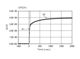
- FIG. 7 is a graph for explaining the response characteristics of a photodiode.
- FIG. 8 is a graph showing an enlarged view of a portion of the first and second regions in FIG. 7.
- the vertical axis represents the photocurrent Ip output from the photodiode PD.
- the horizontal axis represents the irradiation time of light from the light source (first light source 61 or second light source 62), with the time when the light source (first light source 61 or second light source 62) begins to turn on being set as 0.
- the response characteristics of the photodiode PD have a first region A1 where the slope of the photocurrent Ip is large, and a second region A2 where the slope of the photocurrent Ip is small.
- the first region A1 the magnitude (sensitivity) of the photocurrent Ip is small compared to the second region A2, but the time required for measurement is short.
- the second region A2 the irradiation time of light from the light source (first light source 61 or second light source 62) is longer compared to the first region A1, and the magnitude (sensitivity) of the photocurrent Ip is large.
- the first readout period RD1 of the first mode M1 described above corresponds to the first region A1 in the response characteristics of the photodiode PD.
- the second readout period RD2 of the second mode M2 corresponds to the second region A2 in the response characteristics of the photodiode PD.
- the detection device 1 executes detection in the first mode M1 and can perform detection with a short measurement period using the first region A1 in the response characteristics of the photodiode PD.
- the detection device 1 executes detection in the second mode M2 and can perform detection with high sensitivity using the second region A2 in the response characteristics of the photodiode PD.
- the detection device 1 can use the response characteristics of the photodiode PD to perform appropriate driving depending on the type of object to be detected or the type of biometric information. This allows the detection device 1 to improve detection accuracy depending on the type of object to be detected or the type of biometric information.
- the timing waveform diagrams shown in Figures 5 and 6 are merely examples and can be modified as appropriate.
- the first light source 61 irradiates near-infrared light and the second light source 62 irradiates red light, but this is not limited to this.
- the first light source 61 may irradiate infrared light.
- the second light source 62 may irradiate green light.
- the first light source 61 and the second light source 62 are turned on in synchronization with the first readout period RD1 in the first mode M1.
- the first light source 61 is turned on in synchronization with the second readout period RD2 in the second mode M2.
- this is not limited to the above, and the first light source 61 and the second light source 62 only need to be turned on during at least the first readout period RD1 in the first mode M1.
- the period during which the first light source 61 and the second light source 62 are turned on may be longer than the first readout period RD1.
- the first light source 61 or the second light source 62 may be turned on in the first mode M1, and the first readout period RD1 may start after a predetermined period has elapsed.
- the first light source 61 is turned on in the second mode M2 at least for the second readout period RD2.
- the period during which the first light source 61 is turned on may be longer than the second readout period RD2.
- the second readout period RD2 may start after the first light source 61 is turned on and a predetermined period has elapsed.
- the first light source 61 is turned on and the second light source 62 is turned off during multiple second read periods RD2, but this is not limited to this.
- the first light source 61 may be turned off and the second light source 62 may be turned on during multiple second read periods RD2.
Landscapes
- Health & Medical Sciences (AREA)
- Life Sciences & Earth Sciences (AREA)
- Physics & Mathematics (AREA)
- Engineering & Computer Science (AREA)
- Medical Informatics (AREA)
- Animal Behavior & Ethology (AREA)
- Veterinary Medicine (AREA)
- Public Health (AREA)
- Biophysics (AREA)
- Pathology (AREA)
- Biomedical Technology (AREA)
- Heart & Thoracic Surgery (AREA)
- General Health & Medical Sciences (AREA)
- Molecular Biology (AREA)
- Surgery (AREA)
- Theoretical Computer Science (AREA)
- General Physics & Mathematics (AREA)
- Cardiology (AREA)
- Multimedia (AREA)
- Physiology (AREA)
- Spectroscopy & Molecular Physics (AREA)
- Optics & Photonics (AREA)
- Human Computer Interaction (AREA)
- Electromagnetism (AREA)
- Photometry And Measurement Of Optical Pulse Characteristics (AREA)
Priority Applications (2)
| Application Number | Priority Date | Filing Date | Title |
|---|---|---|---|
| JP2025515162A JPWO2024219258A1 (https=) | 2023-04-18 | 2024-04-05 | |
| US19/357,987 US20260033755A1 (en) | 2023-04-18 | 2025-10-14 | Detection device |
Applications Claiming Priority (2)
| Application Number | Priority Date | Filing Date | Title |
|---|---|---|---|
| JP2023-067884 | 2023-04-18 | ||
| JP2023067884 | 2023-04-18 |
Related Child Applications (1)
| Application Number | Title | Priority Date | Filing Date |
|---|---|---|---|
| US19/357,987 Continuation US20260033755A1 (en) | 2023-04-18 | 2025-10-14 | Detection device |
Publications (1)
| Publication Number | Publication Date |
|---|---|
| WO2024219258A1 true WO2024219258A1 (ja) | 2024-10-24 |
Family
ID=93152887
Family Applications (1)
| Application Number | Title | Priority Date | Filing Date |
|---|---|---|---|
| PCT/JP2024/014073 Ceased WO2024219258A1 (ja) | 2023-04-18 | 2024-04-05 | 検出装置 |
Country Status (3)
| Country | Link |
|---|---|
| US (1) | US20260033755A1 (https=) |
| JP (1) | JPWO2024219258A1 (https=) |
| WO (1) | WO2024219258A1 (https=) |
Citations (6)
| Publication number | Priority date | Publication date | Assignee | Title |
|---|---|---|---|---|
| JP2006221514A (ja) * | 2005-02-14 | 2006-08-24 | Canon Inc | 生体認証装置及び画像取得方法 |
| JP2014014439A (ja) * | 2012-07-06 | 2014-01-30 | Fujifilm Corp | 内視鏡システム、内視鏡システムのプロセッサ装置、及び内視鏡用制御プログラム |
| WO2019146228A1 (ja) * | 2018-01-29 | 2019-08-01 | ソニー株式会社 | 医療用撮像装置及び医療用撮像方法 |
| JP2019170542A (ja) * | 2018-03-27 | 2019-10-10 | キヤノン株式会社 | 生体の測定装置及びプログラム |
| WO2020137129A1 (ja) * | 2018-12-28 | 2020-07-02 | 株式会社ジャパンディスプレイ | 検出装置 |
| WO2023032863A1 (ja) * | 2021-09-01 | 2023-03-09 | 株式会社ジャパンディスプレイ | 検出装置 |
-
2024
- 2024-04-05 JP JP2025515162A patent/JPWO2024219258A1/ja active Pending
- 2024-04-05 WO PCT/JP2024/014073 patent/WO2024219258A1/ja not_active Ceased
-
2025
- 2025-10-14 US US19/357,987 patent/US20260033755A1/en active Pending
Patent Citations (6)
| Publication number | Priority date | Publication date | Assignee | Title |
|---|---|---|---|---|
| JP2006221514A (ja) * | 2005-02-14 | 2006-08-24 | Canon Inc | 生体認証装置及び画像取得方法 |
| JP2014014439A (ja) * | 2012-07-06 | 2014-01-30 | Fujifilm Corp | 内視鏡システム、内視鏡システムのプロセッサ装置、及び内視鏡用制御プログラム |
| WO2019146228A1 (ja) * | 2018-01-29 | 2019-08-01 | ソニー株式会社 | 医療用撮像装置及び医療用撮像方法 |
| JP2019170542A (ja) * | 2018-03-27 | 2019-10-10 | キヤノン株式会社 | 生体の測定装置及びプログラム |
| WO2020137129A1 (ja) * | 2018-12-28 | 2020-07-02 | 株式会社ジャパンディスプレイ | 検出装置 |
| WO2023032863A1 (ja) * | 2021-09-01 | 2023-03-09 | 株式会社ジャパンディスプレイ | 検出装置 |
Also Published As
| Publication number | Publication date |
|---|---|
| US20260033755A1 (en) | 2026-02-05 |
| JPWO2024219258A1 (https=) | 2024-10-24 |
Similar Documents
| Publication | Publication Date | Title |
|---|---|---|
| US11888080B2 (en) | Detection device including light sources along an outer circumference of two detection areas each of the detection areas having a specific scan direction | |
| JP7255818B2 (ja) | 検出装置 | |
| JP7253751B2 (ja) | 検出装置 | |
| CN118984677A (zh) | 检测装置 | |
| US20250008759A1 (en) | Detection device | |
| JP7645689B2 (ja) | 検出装置及び撮像装置 | |
| JP7796218B2 (ja) | 検出装置 | |
| CN116134620A (zh) | 检测装置 | |
| US20250063882A1 (en) | Detection device | |
| US20240381676A1 (en) | Detection device | |
| WO2024219258A1 (ja) | 検出装置 | |
| US20240324259A1 (en) | Detection device | |
| WO2024209907A1 (ja) | 検出装置 | |
| US20260025604A1 (en) | Detection device | |
| WO2025079423A1 (ja) | 検出装置 | |
| US20250255085A1 (en) | Detection device | |
| US20250310628A1 (en) | Detection device | |
| US20240423003A1 (en) | Detection device | |
| US20250316111A1 (en) | Detection device | |
| WO2025105160A1 (ja) | 検出装置 | |
| WO2024262191A1 (ja) | 検出装置及び検出装置の製造方法 | |
| US20230301125A1 (en) | Detection device | |
| WO2024257502A1 (ja) | 検出装置 | |
| WO2025037531A1 (ja) | 検出装置 | |
| WO2026042483A1 (ja) | 検出装置及び検出装置の製造方法 |
Legal Events
| Date | Code | Title | Description |
|---|---|---|---|
| 121 | Ep: the epo has been informed by wipo that ep was designated in this application |
Ref document number: 24792533 Country of ref document: EP Kind code of ref document: A1 |
|
| ENP | Entry into the national phase |
Ref document number: 2025515162 Country of ref document: JP Kind code of ref document: A |
|
| WWE | Wipo information: entry into national phase |
Ref document number: 2025515162 Country of ref document: JP |
|
| NENP | Non-entry into the national phase |
Ref country code: DE |
|
| 122 | Ep: pct application non-entry in european phase |
Ref document number: 24792533 Country of ref document: EP Kind code of ref document: A1 |