WO2024214645A1 - 伝送回路基板及び積層フィルム - Google Patents
伝送回路基板及び積層フィルム Download PDFInfo
- Publication number
- WO2024214645A1 WO2024214645A1 PCT/JP2024/014066 JP2024014066W WO2024214645A1 WO 2024214645 A1 WO2024214645 A1 WO 2024214645A1 JP 2024014066 W JP2024014066 W JP 2024014066W WO 2024214645 A1 WO2024214645 A1 WO 2024214645A1
- Authority
- WO
- WIPO (PCT)
- Prior art keywords
- resin layer
- tetrafluoroethylene
- layer
- polymer
- laminate film
- Prior art date
- Legal status (The legal status is an assumption and is not a legal conclusion. Google has not performed a legal analysis and makes no representation as to the accuracy of the status listed.)
- Ceased
Links
Classifications
-
- H—ELECTRICITY
- H05—ELECTRIC TECHNIQUES NOT OTHERWISE PROVIDED FOR
- H05K—PRINTED CIRCUITS; CASINGS OR CONSTRUCTIONAL DETAILS OF ELECTRIC APPARATUS; MANUFACTURE OF ASSEMBLAGES OF ELECTRICAL COMPONENTS
- H05K1/00—Printed circuits
- H05K1/02—Details
- H05K1/03—Use of materials for the substrate
- H05K1/0313—Organic insulating material
-
- B—PERFORMING OPERATIONS; TRANSPORTING
- B32—LAYERED PRODUCTS
- B32B—LAYERED PRODUCTS, i.e. PRODUCTS BUILT-UP OF STRATA OF FLAT OR NON-FLAT, e.g. CELLULAR OR HONEYCOMB, FORM
- B32B15/00—Layered products comprising a layer of metal
- B32B15/04—Layered products comprising a layer of metal comprising metal as the main or only constituent of a layer, which is next to another layer of the same or of a different material
- B32B15/08—Layered products comprising a layer of metal comprising metal as the main or only constituent of a layer, which is next to another layer of the same or of a different material of synthetic resin
- B32B15/082—Layered products comprising a layer of metal comprising metal as the main or only constituent of a layer, which is next to another layer of the same or of a different material of synthetic resin comprising vinyl resins; comprising acrylic resins
-
- B—PERFORMING OPERATIONS; TRANSPORTING
- B32—LAYERED PRODUCTS
- B32B—LAYERED PRODUCTS, i.e. PRODUCTS BUILT-UP OF STRATA OF FLAT OR NON-FLAT, e.g. CELLULAR OR HONEYCOMB, FORM
- B32B15/00—Layered products comprising a layer of metal
- B32B15/04—Layered products comprising a layer of metal comprising metal as the main or only constituent of a layer, which is next to another layer of the same or of a different material
- B32B15/08—Layered products comprising a layer of metal comprising metal as the main or only constituent of a layer, which is next to another layer of the same or of a different material of synthetic resin
- B32B15/088—Layered products comprising a layer of metal comprising metal as the main or only constituent of a layer, which is next to another layer of the same or of a different material of synthetic resin comprising polyamides
-
- H—ELECTRICITY
- H05—ELECTRIC TECHNIQUES NOT OTHERWISE PROVIDED FOR
- H05K—PRINTED CIRCUITS; CASINGS OR CONSTRUCTIONAL DETAILS OF ELECTRIC APPARATUS; MANUFACTURE OF ASSEMBLAGES OF ELECTRICAL COMPONENTS
- H05K1/00—Printed circuits
- H05K1/02—Details
- H05K1/03—Use of materials for the substrate
Definitions
- the present invention relates to a transmission circuit board and a laminated film.
- the present invention relates to a transmission circuit board that has small transmission loss even in the high frequency range, and a laminated film that constitutes such a transmission circuit board and has a resin layer that contains a tetrafluoroethylene-based polymer.
- Patent Document 1 discloses a three-layer film in which a polyimide film is used as a base film and a tetrafluoroethylene polymer layer is provided on each of its two sides.
- the three-layer film proposed in Patent Document 1 has mechanical properties based on polyimide and electrical properties and heat resistance based on tetrafluoroethylene-based polymers, and is useful as a material applicable to electrical and electronic fields such as printed circuit boards and wire coatings.
- the present inventors found that in a film having a polyimide base film and a resin layer containing a tetrafluoroethylene-based polymer, when the thicknesses of both are within a specific range and the thickness of the resin layer containing a tetrafluoroethylene-based polymer is set to a specific ratio, the transmission loss in the high frequency range is improved.Then, they found that this can be effectively applied to the production of transmission circuit boards, and arrived at the present invention.
- An object of the present invention is to provide a transmission circuit board which has small transmission loss even in the high frequency range and excellent electrical characteristics, and a laminate film which constitutes such a transmission circuit board and has a resin layer containing a tetrafluoroethylene-based polymer.
- a transmission circuit board comprising a first laminate film, a metal pattern layer, and a second laminate film laminated in this order, the first laminate film comprising a first resin layer containing a tetrafluoroethylene-based polymer, a polyimide layer, and a second resin layer containing a tetrafluoroethylene-based polymer laminated in this order, the second laminate film comprising a third resin layer containing a tetrafluoroethylene-based polymer, a polyimide layer, and a fourth resin layer containing a tetrafluoroethylene-based polymer laminated in this order, the first laminate film, the metal pattern layer, and the second laminate film having a total thickness of more than 150 ⁇ m and not more than 400 ⁇ m, the total thickness being thickness S and the proportion of the total thickness of the third resin layer and the fourth resin layer to thickness S being proportion F, wherein thickness S and proportion F satisfy the formula represented by the following formula (1).
- a transmission circuit board comprising a first laminate film, a metal pattern layer, and a second laminate film laminated in this order, the first laminate film comprising a first resin layer containing a tetrafluoroethylene-based polymer, a polyimide layer, and a second resin layer containing a tetrafluoroethylene-based polymer laminated in this order, and the second laminate film comprising a third resin layer containing a tetrafluoroethylene-based polymer, a polyimide layer, and a fourth resin layer containing a tetrafluoroethylene-based polymer laminated in this order, the ratio of the total thickness of the first resin layer, the second resin layer, the third resin layer, and the fourth resin layer to the total thickness of the first laminate film, the metal pattern layer, and the second laminate film is more than 50% and not more than 75%, and the total thickness is more than 150 ⁇ m and not more than 400 ⁇ m.
- a laminated film comprising a first resin layer containing a tetrafluoroethylene-based polymer, a polyimide layer, and a second resin layer containing a tetrafluoroethylene-based polymer laminated in this order, wherein a total thickness of the first resin layer, the polyimide layer, and the second resin layer is more than 50 ⁇ m and not more than 200 ⁇ m, and wherein the total thickness is Sa and a ratio of the total thickness of the first resin layer and the second resin layer to the thickness Sa is Fa, the thickness Sa and the ratio Fa satisfy the following formula (11): Proportion Fa ⁇ 43872 ⁇ (thickness Sa) ⁇ 2.14 (11) [8] The laminate film of [7], wherein the thickness of the first resin layer and the second resin layer is more than 20 ⁇ m and not more than 100 ⁇ m, and the thickness of the polyimide layer is not more than 50 ⁇ m.
- a laminated film comprising a first resin layer containing a tetrafluoroethylene-based polymer, a polyimide layer, and a second resin layer containing a tetrafluoroethylene-based polymer laminated in this order, wherein the total thickness of the first resin layer, the polyimide layer, and the second resin layer is more than 50 ⁇ m and not more than 200 ⁇ m, and the ratio of the total thickness of the first resin layer and the second resin layer to the total thickness is more than 50% and not more than 75%.
- the present invention provides a transmission circuit board that has low transmission loss even in the high frequency range and has excellent electrical properties, and a laminate film that constitutes such a transmission circuit board and has a resin layer that contains a tetrafluoroethylene-based polymer.
- Average particle diameter (D50) is the volume-based cumulative 50% diameter of particles determined by a laser diffraction/scattering method.
- the particle size distribution is measured by a laser diffraction/scattering method, a cumulative curve is calculated with the total volume of the particle group as 100%, and the particle diameter is the point on the cumulative curve where the cumulative volume is 50%.
- the D50 of particles is determined by dispersing the particles in water and analyzing them by a laser diffraction/scattering method using a laser diffraction/scattering type particle size distribution measuring device (LA-920 measuring device, manufactured by Horiba, Ltd.).
- Melting temperature is the temperature corresponding to the maximum of the melting peak of a polymer as measured by differential scanning calorimetry (DSC).
- Glass transition temperature (Tg) is a value measured by analyzing a polymer using dynamic mechanical analysis (DMA) method.
- the "viscosity” is determined by measuring the composition using a Brookfield viscometer at 25° C. and a rotation speed of 30 rpm. The measurement is repeated three times, and the average value of the three measured values is calculated.
- the "thixotropy ratio” is a value calculated by dividing the viscosity ⁇ 1 of the composition measured at a rotation speed of 30 rpm by the viscosity ⁇ 2 measured at a rotation speed of 60 rpm.
- a "unit" in a polymer means an atomic group based on a monomer formed by polymerization of the monomer.
- the unit may be a unit formed directly by a polymerization reaction, or may be a unit in which a part of the unit is converted into a different structure by processing the polymer.
- a unit based on monomer a is also simply referred to as a "monomer a unit.”
- the first transmission circuit board of the present invention (hereinafter also referred to as “this transmission circuit board 1") is a transmission circuit board in which a first laminate film, a metal pattern layer, and a second laminate film are laminated in this order, the first laminate film is a first resin layer containing a tetrafluoroethylene-based polymer (hereinafter also referred to as "F polymer”), a polyimide layer, and a second resin layer containing an F polymer, which are laminated in this order, and the second laminate film is a third resin layer containing an F polymer, a polyimide layer, and a fourth resin layer containing an F polymer, which are laminated in this order, the first laminate film, the metal pattern layer, and the second laminate film have a total thickness of more than 150 ⁇ m and 400 ⁇ m or less, the total thickness is thickness S, and the ratio of the total thickness of the third resin layer and the fourth resin layer to the thickness S is ratio F, the thickness S and the ratio F satisfy the formula represented by the following
- the second transmission circuit board of the present invention (hereinafter also referred to as "this transmission circuit board 2") is a transmission circuit board in which a first laminate film, a metal pattern layer, and a second laminate film are laminated in this order, the first laminate film is a first resin layer containing an F polymer, a polyimide layer, and a second resin layer containing an F polymer laminated in this order, the second laminate film is a third resin layer containing an F polymer, a polyimide layer, and a fourth resin layer containing an F polymer laminated in this order, the ratio of the total thickness of the first resin layer, the second resin layer, the third resin layer, and the fourth resin layer to the total thickness of the first laminate film, the metal pattern layer, and the second laminate film is more than 50% and not more than 75%, and the total thickness is more than 150 ⁇ m and not more than 400 ⁇ m.
- the present transmission circuit board 1 and the present transmission circuit board 2 may be collectively referred to as the present transmission circuit board.
- the first laminate film of the present invention (hereinafter also referred to as "the laminate film 1") is a laminate film in which a first resin layer containing an F polymer, a polyimide layer, and a second resin layer containing an F polymer are laminated in this order, the total thickness of the first resin layer, the polyimide layer, and the second resin layer is more than 50 ⁇ m and not more than 200 ⁇ m, and the total thickness is Sa and the ratio of the total thickness of the first resin layer and the second resin layer to the thickness Sa is Fa, the thickness Sa and the ratio Fa satisfy the formula represented by the following formula (11). Proportion Fa ⁇ 43872 ⁇ (thickness Sa) ⁇ 2.14 (11)
- the second laminate film of the present invention (hereinafter also referred to as "the present laminate film 2") comprises a first resin layer containing an F polymer, a polyimide layer, and a second resin layer containing an F polymer laminated in this order, the total thickness of the first resin layer, the polyimide layer, and the second resin layer is more than 50 ⁇ m and not more than 200 ⁇ m, and the ratio of the total thickness of the first resin layer and the second resin layer to the total thickness is more than 50% and not more than 75%.
- the present laminate film 1 and the present laminate film 2 may be collectively referred to as the present laminate film.
- the present transmission circuit board is preferably formed by laminating the present laminate film, a metal pattern layer, and the present laminate film in this order.
- Each laminate film layer has excellent physical properties, such as mechanical properties, heat resistance, and electrical properties (low linear expansion coefficient, low dielectric constant, and low dielectric tangent), based on the polyimide layer and the resin layer containing F polymer, and the transmission loss is particularly small in the high frequency range.
- the thickness of each layer In a three-layer laminate film in which a first resin layer containing an F polymer, a polyimide layer, and a second resin layer containing an F polymer are laminated in this order, the following has been taken into consideration regarding the thickness of each layer. That is, the polyimide layer is made to have a certain thickness from the viewpoint of ensuring mechanical properties such as foldability of the laminate film. On the other hand, the thicknesses of the first resin layer and the second resin layer are made equal to each other from the viewpoint of suppressing warping and ensuring dimensional stability, since the linear expansion coefficient of the F polymer is high, and are made as thin as possible within the range in which heat resistance and electrical properties can be ensured from the viewpoint of making the entire printed circuit board thin.
- the present inventors unexpectedly found that the ratio of the total thickness of the first resin layer and the second resin layer to the total thickness of the first resin layer, the polyimide layer, and the second resin layer (i.e., the thickness of the entire laminate film) is important from the viewpoint of improving the transmission loss of the laminate film in the high frequency range. And, the present inventors found that by setting the total thickness and the total thickness of the first resin layer and the second resin layer to the total thickness within a specific range, a laminate film that suppresses warping and is excellent in mechanical properties such as heat resistance and foldability, and electrical properties, as well as further reducing transmission loss, i.e., laminate film 2, can be obtained. It has also been found that when the first resin layer and the second resin layer contain a specific F polymer, which will be described later, such an effect is significantly exhibited.
- the F polymer constituting the present laminate film is a polymer containing units (hereinafter also referred to as "TFE units") based on tetrafluoroethylene (hereinafter also referred to as "TFE").
- the F polymer is preferably heat-fusible.
- a heat-fusible polymer means a polymer that has a temperature at which the melt flow rate is 1 to 1000 g/10 min under a load of 49 N.
- the melting temperature of the F polymer is preferably 200° C. or higher, more preferably 260° C. or higher.
- the melting temperature of the F polymer is preferably 325° C. or lower, more preferably 320° C. or lower.
- the glass transition temperature of the F polymer is preferably 60° C. or higher, more preferably 75° C. or higher.
- the glass transition temperature of the F polymer is preferably 120° C. or lower, more preferably 100° C. or lower.
- the fluorine content of the F polymer is preferably 70% by mass or more, more preferably 72 to 76% by mass.
- the surface tension of the F polymer is preferably 16 to 26 mN/m.
- the surface tension of the F polymer can be measured by placing a droplet of a mixture for wetting tension testing (manufactured by Wako Pure Chemical Industries, Ltd.) specified in JIS K 6768 on a flat plate made of the F polymer.
- F polymer is preferably the polymer (ETFE) that comprises TFE unit and ethylene-based unit, the polymer (PFA) that comprises TFE unit and perfluoro(alkyl vinyl ether) (PAVE)-based unit (PAVE unit), the polymer (FEP) that comprises TFE unit and hexafluoropropylene-based unit, more preferably PFA and FEP, and even more preferably PFA.
- PAVE is preferably CF 2 ⁇ CFOCF 3 , CF 2 ⁇ CFOCF 2 CF 3 or CF 2 ⁇ CFOCF 2 CF 2 CF 3 (hereinafter also referred to as “PPVE”), and more preferably PPVE.
- the F polymer preferably has an oxygen-containing polar group, more preferably has a hydroxyl- or carbonyl-containing group, and even more preferably has a carbonyl-containing group.
- the adhesion between the first resin layer and the second resin layer in the laminate film and the polyimide layer is more likely to be improved, and the adhesion of the outermost surface of the laminate film is also likely to be improved.
- the laminate film is more likely to have excellent physical properties such as heat resistance and electrical properties (low linear expansion coefficient, low dielectric constant and low dielectric tangent), and the transmission loss in the high frequency range of a transmission circuit board formed therefrom is more likely to be reduced.
- the hydroxyl-containing group is preferably a group containing an alcoholic hydroxyl group, more preferably --CF 2 CH 2 OH or --C(CF 3 ) 2 OH.
- the carbonyl group-containing group is preferably a carboxyl group, an alkoxycarbonyl group, an amide group, an isocyanate group, a carbamate group (-OC(O)NH 2 ), an acid anhydride residue (-C(O)OC(O)-), an imide residue (-C(O)NHC(O)-, etc.), a formyl group, a halogenoformyl group, a urethane group (-NHC(O)O-), a carbamoyl group (-C(O)-NH 2 ), a ureido group (-NH-C(O)-NH 2 ), an oxamoyl group (-NH-C(O)-C(O)-NH 2 ) or a carbonate group (-OC(O)
- the number of oxygen-containing polar groups in the F polymer is preferably 10 to 5000, more preferably 100 to 3000, per 1 ⁇ 10 6 carbon atoms in the main chain.
- the number of oxygen-containing polar groups in the F polymer can be quantified by the composition of the polymer or the method described in WO 2020/145133.
- the oxygen-containing polar group may be contained in a unit based on a monomer in the F polymer, or may be contained in a terminal group of the main chain of the F polymer, with the former being preferred.
- Examples of the latter include F polymers having an oxygen-containing polar group as a terminal group derived from a polymerization initiator, a chain transfer agent, etc., and F polymers obtained by subjecting F polymers to plasma treatment or ionizing radiation treatment.
- the F polymer is preferably a polymer (1) that contains TFE units and PAVE units, contains 2.0 to 5.0 mol% of PAVE units relative to the total units, and does not have an oxygen-containing polar group, or a polymer (2) that contains TFE units and PAVE units and has an oxygen-containing polar group. If such an F polymer is used, spherulites with a relatively small radius are likely to be formed. Therefore, the first resin layer and the second resin layer in this laminate film have high surface smoothness and further improved adhesion to the polyimide layer.
- Polymer (1) is composed of only TFE units and PAVE units, and more preferably contains PAVE units in an amount of more than 2.5 mol% and not more than 5.0 mol% relative to the total units.
- polymer (1) does not have an oxygen-containing polar group means that the number of oxygen-containing polar groups that the polymer has is less than 500 per 1 x 10⁶ carbon atoms that constitute the polymer main chain.
- the number of the oxygen-containing polar groups is preferably 100 or less, more preferably less than 50.
- the lower limit of the number of the oxygen-containing polar groups is 1.
- the polymer (1) may be produced using a polymerization initiator or a chain transfer agent that does not generate an oxygen-containing polar group as a terminal group of the polymer chain, or may be produced by fluorinating an F polymer having an oxygen-containing polar group (such as an F polymer having an oxygen-containing polar group derived from a polymerization initiator at the terminal group of the polymer main chain).
- fluorination method include a method using fluorine gas (see JP 2019-194314 A, etc.).
- the polymer (2) is preferably a thermally meltable F polymer having a carbonyl group-containing group, including TFE units and PAVE units, more preferably a polymer including TFE units, PAVE units, and units based on a monomer having a carbonyl group-containing group, and including these units in the order of 90 to 99 mol%, 0.99 to 9.97 mol%, and 0.01 to 3 mol% relative to the total units.
- F polymers include the polymers described in WO 2018/16644.
- the monomer having a carbonyl group-containing group is preferably itaconic anhydride, citraconic anhydride, or 5-norbornene-2,3-dicarboxylic anhydride (hereinafter also referred to as "NAH"), and more preferably NAH.
- the polyimide layer constituting the present laminated film is preferably formed from a polyimide base film (hereinafter also referred to as "polyimide film").
- the polyimide film preferably has a high yield strength, and specifically, the stress at 5% strain is preferably 180 MPa or more and 500 MPa or less.
- the polyimide film is preferably difficult to plastically deform, and specifically, the stress at 15% strain is preferably 225 MPa or more and 580 MPa or less.
- the polyimide layer constituting the present laminate film is a polyimide film having the above-mentioned properties, the absolute value of the linear expansion coefficient of the present laminate film can be easily made sufficiently low, and the occurrence of warping can be suppressed.
- the tensile modulus of the polyimide film at 320° C. is preferably 0.2 GPa or more and 10 GPa or less, from the viewpoint of processability and flexibility of the present laminate film.
- a first resin layer, a polyimide layer, and a second resin layer containing an F polymer are laminated in this order. It is preferable that the first resin layer and the polyimide layer, and the polyimide layer and the second resin layer are in direct contact with each other. In other words, it is preferable that the resin layers are directly formed (laminated) on both surfaces of the polyimide film without performing surface treatment with a silane coupling agent, adhesive, or the like. In this case, the physical properties of the laminated film based on the F polymer and polyimide layer are more likely to be exhibited. In addition, in this laminated film, due to the above-mentioned configuration, high adhesion is easily exhibited between the polyimide layer and the resin layer even if the polyimide layer and the resin layer are in direct contact with each other.
- the total thickness of the first resin layer, the polyimide layer, and the second resin layer of the present laminate film is more than 50 ⁇ m and not more than 200 ⁇ m.
- the total thickness is preferably 65 ⁇ m or more, and more preferably 80 ⁇ m or more.
- the total thickness is preferably 180 ⁇ m or less, and more preferably 160 ⁇ m or less.
- the thickness of each of the first and second resin layers is preferably more than 20 ⁇ m and not more than 100 ⁇ m.
- the thickness of each of the first and second resin layers is more preferably 25 ⁇ m or more, even more preferably more than 25 ⁇ m, and particularly preferably 30 ⁇ m or more.
- the thickness is more preferably 75 ⁇ m or less, even more preferably 65 ⁇ m or less, and particularly preferably 60 ⁇ m or less.
- the first and second resin layers may have different thicknesses, but are preferably equal in thickness, in which case the linear expansion coefficients of the two resin layers become closer to each other, making the laminate film less susceptible to warping.
- the thickness of the polyimide layer is preferably 15 ⁇ m or more, more preferably 20 ⁇ m or more, and even more preferably 25 ⁇ m or more.
- the thickness of the polyimide layer is preferably 50 ⁇ m or less, and more preferably 40 ⁇ m or less.
- the thicknesses of the present laminated film, the polyimide film constituting the polyimide layer, the first resin layer, and the second resin layer are measured using a contact thickness meter DG-525H (manufactured by Ono Sokki Co., Ltd.) with a probe AA-026 ( ⁇ 10 mm, SR7).
- the ratio of the total thickness of the first resin layer and the second resin layer to the total thickness is more than 50% and not more than 75%.
- the ratio is preferably 55% or more, and more preferably 60% or more.
- the ratio is preferably 72% or less, and more preferably 70% or less.
- the ratio of the total thickness of the first resin layer and the second resin layer to the thickness of the polyimide layer is preferably more than 1 and 2 or less.
- the physical properties of the polyimide film and the electrical properties of the F polymer such as low dielectric constant and low dielectric loss tangent, and the physical properties of low water absorption, are easily balanced.
- warping and peeling of the laminated film are easily suppressed, and the transmission loss in the high frequency range is easily improved.
- the content of the F polymer in each of the first and second resin layers is preferably 80% by mass or more, more preferably 90% by mass or more.
- the content may be 100% by mass or less.
- the first resin layer and the second resin layer preferably have an oxygen-containing polar group on their surfaces (the surfaces opposite to the polyimide film). The presence of the oxygen-containing polar group on the surface of the layer increases the adhesion, and the adhesive strength between the film and a metal foil or other members bonded to the surface of the film can be improved.
- the oxygen-containing polar group is preferably a hydroxyl group-containing group or a carbonyl group-containing group.
- Methods for making the oxygen-containing polar group present on the surface of the first resin layer and the second resin layer include a method of using an F polymer having an oxygen-containing polar group, or a method of subjecting the surfaces of the first resin layer and the second resin layer to a surface treatment such as corona discharge treatment, plasma treatment, UV ozone treatment, excimer treatment, chemical etching, or silane coupling treatment to introduce the oxygen-containing polar group.
- a surface treatment such as corona discharge treatment, plasma treatment, UV ozone treatment, excimer treatment, chemical etching, or silane coupling treatment to introduce the oxygen-containing polar group.
- the dielectric constant (relative dielectric constant) of the present laminated film is preferably 2.0 to 3.0.
- the dielectric loss tangent of the present laminate film is preferably 0.0001 to 0.003.
- the dielectric loss tangent of the present laminate film is preferably less than 0.003, more preferably 0.0025 or less, and even more preferably 0.002 or less.
- the absolute value of the linear expansion coefficient of the present laminate film is preferably 30 ppm/° C. or less, more preferably 15 ppm/° C. or less. In this case, the occurrence of warping of the present laminate film is effectively prevented regardless of the temperature of the atmosphere in which the present laminate film is placed.
- the lower limit of the absolute value of the linear expansion coefficient of the present laminate film is 0 ppm/° C.
- the peel strength of the laminated film is preferably 10 N/cm or more, more preferably 15 N/cm or more. In this case, the laminated film can be suitably used as a printed circuit board material or a coating material for a metal conductor (a coating material for an electric wire, etc.).
- the upper limit of the peel strength of the laminated film is 100 N/cm.
- the water absorption of the present laminated film is preferably 0.1% or less. In this case, the present laminated film is more resistant to water vapor permeation and exhibits excellent insulation properties for a long period of time, and is therefore particularly suitable for use as a coating material for metal conductors.
- the water absorption is determined in accordance with ASTM D570.
- the first and second resin layers in this laminate film are preferably formed from a resin film containing an F polymer.
- the resin films containing an F polymer that will become the first and second resin layers are placed on both surfaces of a polyimide base film, and laminated, preferably by heat pressing, to form the first resin layer, the polyimide layer, and the second resin layer, thereby producing this laminate film.
- the first resin layer and the second resin layer in the present laminate film are preferably formed from a liquid composition containing F polymer particles (hereinafter also referred to as "F particles”) and a dispersion medium.
- F particles F polymer particles
- the present laminate film can be manufactured by a method in which a liquid composition containing F particles and a dispersion medium (hereinafter also referred to as “the present liquid composition”) is applied and disposed on both surfaces of a polyimide base film (hereinafter also referred to as "polyimide film”), and then heated to form the first resin layer and the second resin layer.
- the F particles preferably have an average particle size (D50) of 0.3 ⁇ m or more and less than 10 ⁇ m.
- the D50 of the F particles is preferably 0.5 ⁇ m or more, more preferably 1.0 ⁇ m or more.
- the D50 of the F particles is preferably less than 10 ⁇ m, more preferably 8 ⁇ m or less.
- the liquid composition is likely to have excellent dispersibility and processability, and the resin layer formed from the liquid composition is likely to have excellent physical properties such as heat resistance, electrical properties (low linear expansion coefficient, low dielectric constant and low dielectric tangent), and surface appearance.
- the F particles are particles containing an F polymer, and preferably consist of an F polymer. The F particles may be used alone or in combination of two or more kinds.
- the dispersion medium contained in the present liquid composition is preferably at least one selected from the group consisting of water, amides, ketones and esters.
- the amide include N-methyl-2-pyrrolidone, N,N-dimethylformamide, N,N-dimethylacetamide, N,N-dimethylpropanamide, 3-methoxy-N,N-dimethylpropanamide, 3-butoxy-N,N-dimethylpropanamide, N,N-diethylformamide, hexamethylphosphoric triamide, and 1,3-dimethyl-2-imidazolidinone.
- ketone examples include acetone, methyl ethyl ketone, methyl isopropyl ketone, methyl isobutyl ketone, methyl n-pentyl ketone, methyl isopentyl ketone, 2-heptanone, cyclopentanone, cyclohexanone, and cycloheptanone.
- ester examples include methyl acetate, ethyl acetate, butyl acetate, methyl lactate, ethyl lactate, methyl pyruvate, ethyl pyruvate, methyl methoxypropionate, ethyl ethoxypropionate, ethyl 3-ethoxypropionate, ⁇ -butyrolactone, and ⁇ -valerolactone.
- the liquid composition may further contain a surfactant.
- the surfactant is preferably a nonionic surfactant.
- nonionic surfactants include glycol-based surfactants, acetylene-based surfactants, silicone-based surfactants, and fluorine-based surfactants.
- the liquid composition may further contain inorganic particles.
- inorganic particles include silicon compounds such as quartz powder, silica, wollastonite, talc, silicon nitride, silicon carbide, and mica; nitrogen compounds such as boron nitride and aluminum nitride; metal oxides such as aluminum oxide, zinc oxide, titanium oxide, cerium oxide, beryllium oxide, magnesium oxide, nickel oxide, vanadium oxide, copper oxide, iron oxide, and silver oxide; carbon fibers; carbon allotropes such as graphite, graphene, and carbon nanotubes; and metals such as silver and copper.
- silicon compounds such as quartz powder, silica, wollastonite, talc, silicon nitride, silicon carbide, and mica
- nitrogen compounds such as boron nitride and aluminum nitride
- metal oxides such as aluminum oxide, zinc oxide, titanium oxide, cerium oxide, beryllium oxide, magnesium oxide, nickel oxide, vanadium oxide, copper oxide, iron oxide, and silver
- the liquid composition may further contain another resin different from the F polymer.
- Such another resin may be contained in the liquid composition as non-hollow particles, or may be dissolved or dispersed in a liquid dispersion medium (hereinafter also referred to as "liquid dispersion medium") such as a liquid compound constituting the liquid composition.
- liquid dispersion medium such as a liquid compound constituting the liquid composition.
- other resins include polyester resins such as liquid crystalline aromatic polyesters, polyimide resins, polyamideimide resins, epoxy resins, maleimide resins, urethane resins, polyphenylene ether resins, polyphenylene oxide resins, and polyphenylene sulfide resins.
- the other resin is preferably a polyimide or a precursor thereof, and more preferably at least one polyimide or a precursor thereof selected from the group consisting of aromatic polyimide, aromatic polyamic acid, aromatic polyamideimide, and a precursor of aromatic polyamideimide.
- the polyimide or a precursor thereof is preferably contained in the liquid composition as a varnish dissolved in a liquid dispersion medium.
- the content relative to the F particles is preferably 1 to 25% by mass.
- the liquid composition may further contain additives such as thixotropic agents, viscosity regulators, defoamers, dehydrating agents, plasticizers, weather resistance agents, antioxidants, heat stabilizers, lubricants, antistatic agents, brighteners, colorants, conductive agents, release agents, and flame retardants.
- additives such as thixotropic agents, viscosity regulators, defoamers, dehydrating agents, plasticizers, weather resistance agents, antioxidants, heat stabilizers, lubricants, antistatic agents, brighteners, colorants, conductive agents, release agents, and flame retardants.
- the content of F particles in the present liquid composition is preferably 25% by mass or more, more preferably 30% by mass or more, and is preferably 75% by mass or less, more preferably 60% by mass or less.
- the viscosity of the liquid composition is preferably 10 mPa ⁇ s or more, more preferably 100 mPa ⁇ s or more.
- the viscosity of the liquid composition is preferably 10,000 mPa ⁇ s or less, more preferably 3,000 mPa ⁇ s or less.
- the liquid composition has excellent coatability and is easy to form a resin layer having a desired thickness.
- the liquid composition having a viscosity in this range is easy to highly express the physical properties of the F polymer in the resin layer formed therefrom.
- the liquid composition is preferably applied to both surfaces of a polyimide film to first form coating layers of the liquid composition on both surfaces of the polyimide film.
- Methods for applying the liquid composition include the coating method, the droplet ejection method, and the immersion method, and roll coating, knife coating, bar coating, die coating, and spraying methods are preferred.
- the polyimide film having the coating layer is heated to remove the liquid compound constituting the present liquid composition.
- the heating for removing the liquid compound is preferably performed at 100 to 200°C for 0.1 to 30 minutes. In this heating, the liquid compound does not need to be completely removed, and it is sufficient to remove it to the extent that the layer formed by the packing of the F particles can maintain a self-supporting film. In addition, when heating, air may be blown to promote the removal of the liquid compound by air drying.
- the heating for baking the F polymer is preferably carried out in a temperature range equal to or higher than the melting temperature of the F polymer, specifically, at 340 to 400° C. for 0.1 to 30 minutes.
- the heating device for each heating may be an oven or a ventilated drying furnace.
- the heat source in the device may be a contact type heat source (hot air, hot plate, etc.) or a non-contact type heat source (infrared rays, etc.).
- Each heating may be carried out under normal pressure (atmospheric pressure) or under reduced pressure.
- the atmosphere in each heating step may be either an air atmosphere or an inert gas atmosphere (helium gas, neon gas, argon gas, nitrogen gas, etc.).
- the first resin layer and the second resin layer are formed through the steps of coating the liquid composition on the polyimide film and heating. These steps may be performed once each, or may be repeated two or more times.
- the liquid composition may be coated on the surface of the polyimide film to obtain a coating layer, a resin layer may be formed by heating, the liquid composition may be further coated on the surface of the resin layer to form a coating layer, and a second resin layer may be formed by heating.
- the liquid composition may be coated on the surface of the polyimide film to obtain a coating layer, and at the stage where the liquid compound is removed by heating, the liquid composition may be further coated on the surface and a resin layer may be formed by heating. In this manner, the present laminate film having a resin layer containing an F polymer on both surfaces of the polyimide film is obtained.
- the liquid composition contains polyimide or a precursor thereof as a resin other than the F polymer
- the polyimide component derived from the polyimide or the precursor thereof is unevenly distributed on the polyimide layer side of each of the first resin layer and the second resin layer.
- the adhesion between the first resin layer and the second resin layer and the polyimide layer is further improved, and the physical properties based on both layers and the transmission loss in the high frequency range can be reduced.
- the dielectric constant of the first resin layer and the second resin layer is preferably 2.4 or less, more preferably 2.0 or less, and more preferably more than 1.0.
- the dielectric loss tangent of the first resin layer and the second resin layer is preferably 0.0022 or less, more preferably 0.0020 or less, and more preferably more than 0.0010.
- the thermal conductivity of the first resin layer and the second resin layer is preferably 1 W/m ⁇ K or more, and more preferably 3 W/m ⁇ K or more.
- the thermal conductivity of the resin layer means the thermal conductivity in the in-plane direction of the resin layer.
- the linear expansion coefficient of the first resin layer and the second resin layer is preferably 100 ppm/° C. or less, more preferably 80 ppm/° C. or less.
- the lower limit of the linear expansion coefficient of the first resin layer and the second resin layer is 10 ppm/° C.
- the linear expansion coefficient means a value obtained by measuring the linear expansion coefficient of a test piece in the range of 25° C. to 260° C. according to the measurement method specified in JIS C 6471:1995.
- the peel strength between the first and second resin layers and the polyimide film (polyimide layer) is preferably 10 N/cm or more, more preferably 15 N/cm or more, and is preferably 100 N/cm or less.
- the present transmission circuit board comprises a first present laminate film in which a first resin layer containing an F polymer, a polyimide layer, and a second resin layer containing an F polymer are laminated in this order, and a second present laminate film in which a metal pattern layer, a third resin layer containing an F polymer, a polyimide layer, and a fourth resin layer containing an F polymer are laminated in this order, and the ratio of the total thickness of the first resin layer, the second resin layer, the third resin layer, and the fourth resin layer to the total thickness of the first laminate film, the metal pattern layer, and the second laminate film is more than 50% and not more than 75%, and the total thickness is more than 150 ⁇ m and not more than 400 ⁇ m.
- the details of the F polymer and the polyimide layer contained in the first, second, third and fourth resin layers in the first and second present laminate films are as described above.
- the preferred ranges of the thicknesses of the first and second resin layers, the third and fourth resin layers and the polyimide layer are also as described above.
- the total thickness of the present transmission circuit board is more than 150 ⁇ m and not more than 400 ⁇ m, preferably 160 ⁇ m or more, and more preferably 180 ⁇ m or more.
- the total thickness is preferably 360 ⁇ m or less, and more preferably 330 ⁇ m or less.
- the ratio of the total thickness of the first resin layer, the second resin layer, the third resin layer, and the fourth resin layer to the total thickness of the first laminated film, the metal pattern layer, and the second laminated film is more than 50% and not more than 75%.
- the ratio is preferably 55% or more, and more preferably 55% or more.
- the ratio is preferably 72% or less, and more preferably 70% or less.
- the metal pattern layer constituting the present transmission circuit board is preferably encapsulated in an adhesive resin, such as a commercially available thermosetting resin, such as an epoxy resin.
- an adhesive resin such as a commercially available thermosetting resin, such as an epoxy resin.
- the metal pattern layer can be encapsulated using an adhesive resin that is commercially available as a bonding sheet.
- the present transmission circuit board can be preferably produced by forming a metal pattern layer from a metal foil layer formed on one surface of the second present laminate film described above, encapsulating the metal pattern layer using an adhesive resin commercially available as a bonding sheet, and further stacking and pressing the first laminate film onto the surface of the encapsulated metal pattern layer.
- the metal for the metal foil layer examples include metal foils of copper, nickel, aluminum, titanium, alloys thereof, etc. Among these, copper is preferred.
- the ten-point average roughness of the surface of the metal foil layer is preferably 0.01 to 4 ⁇ m, in which case the adhesion to the resin layer is good and a printed circuit board with excellent transmission characteristics is easily obtained.
- the thickness of the metal foil is preferably from 2 to 30 ⁇ m, and more preferably from 3 to 25 ⁇ m.
- the outermost layers on both sides are resin layers containing an F polymer, and because of their excellent adhesion, peeling of the metal layer can be suppressed.
- the transmission circuit board may further have a metal layer or a metal pattern layer on the outermost layer on one or both sides.
- a method for laminating a metal layer on the surface of the present transmission circuit board there is a method in which the present transmission circuit board and a metal foil are heat-pressed.
- the present transmission circuit board is useful as an antenna part, a printed circuit board, an aircraft part, an automobile part, etc., and is particularly useful as a printed circuit board material such as a flexible printed wiring board or a rigid printed wiring board.
- the printed circuit board can be manufactured, for example, by processing the metal layer of the present transmission circuit board, which has a metal layer on one or both sides of the outermost layer, into a conductor circuit (pattern circuit) of a predetermined pattern by etching or the like, or by processing the present transmission circuit board into a pattern circuit by electrolytic plating (semi-additive method (SAP method), modified semi-additive method (MSAP method), etc.).
- an interlayer insulating film may be formed on the pattern circuit, and a conductor circuit may be further formed on the interlayer insulating film.
- a solder resist may be laminated on the pattern circuit, or a coverlay film may be laminated on the pattern circuit.
- the present transmission circuit board and the present laminate film are not limited to the configurations of the above-mentioned embodiments.
- the present transmission circuit board and the present laminate film may have any other configuration in addition to the configurations of the above-mentioned embodiments, or may be replaced with any configuration that produces a similar effect.
- F Particle 1 Particles of a tetrafluoroethylene polymer (melting temperature: 300° C.) containing 97.9 mol %, 0.1 mol %, and 2.0 mol % of TFE units, NAH units, and PPVE units, in that order, and having 1,000 carbonyl group-containing groups per 1 ⁇ 10 6 main chain carbon atoms (D50: 2.4 ⁇ m, Tg: 85° C., specific surface area: 9 m 2 /g).
- Example of laminated film manufacturing By a roll-to-roll process, the liquid composition 1 obtained according to Production Example 1 was applied to one surface of a polyimide film (thickness 25 ⁇ m) by a small-diameter gravure reverse method to form a coating layer, and the film was passed through a ventilation drying oven (oven temperature 150 ° C.) for 3 minutes to remove water and form a dry film. The liquid composition 1 was also applied to the other surface of the polyimide film to form a coating layer, and the film was dried to form a dry film. Next, the substrate with the dry film formed on both sides was passed through a far-infrared oven at an oven temperature of 350 ° C.
- a laminated film 1 was obtained in which a first resin layer (thickness 12.5 ⁇ m) containing an F polymer, a polyimide layer, and a second resin layer (thickness 12.5 ⁇ m) containing an F polymer were laminated in this order.
- Examples 2 to 5 The same procedure as in Example 1 was carried out except that the thickness of the polyimide layer and the thickness of the coating layer of Liquid Composition 1 applied to the polyimide layer were changed as shown in Table 1, to obtain laminate films 2 to 5 in which a first resin layer containing an F polymer, a polyimide layer, and a second resin layer containing an F polymer were laminated in that order.
- Example of Transmission Circuit Board Manufacturing [Example 6] A laminated film 1 and an electrolytic copper foil (manufactured by Fukuda Metal Foil and Powder Co., Ltd., "CF-T49A-DS-HD2", thickness: 12 ⁇ m) were placed opposite each other and thermocompression-bonded under conditions of a temperature of 270° C., a bonding pressure of 1 MPa, and an atmospheric pressure of 10 kPa to obtain a copper foil with a laminated film 1. The copper foil of the copper foil with the laminated film 1 was etched to form a metal pattern layer on the surface of the laminated film 1.
- thermosetting adhesive which is a bonding agent
- a laminated film 2 was placed, followed by similar thermocompression bonding to obtain a transmission circuit board 1 having the laminated film 1, the metal pattern layer encapsulated in the bonding agent, and the laminated film 2 in this order.
- a microstrip line (MSL) was used as the transmission line formed on the printed circuit board, and the characteristic impedance of the line was set to 50 ⁇ .
- the surface of the copper conductor of the printed circuit board was subjected to an anti-rust treatment.
- the calibration method used was TRL calibration (Thru-Reflect-Line calibration).
- the length of the line was set to 50 mm, and the transmission loss per unit length was measured.
- S-parameter hereinafter also referred to as the S value
- Laminate films 6 to 9 in which a first resin layer containing an F polymer, a polyimide layer, and a second resin layer containing an F polymer are laminated in this order are obtained by carrying out the same operation as in Example 1, except that the thickness of the polyimide layer and the thickness of the coating layer of Liquid Composition 1 applied to the polyimide layer are changed as shown in Table 3. Note that laminate films 6 and 8 satisfy the formula represented by formula (11), while laminate films 7 and 9 do not satisfy the formula represented by the following formula (11).
- the absolute value of S21 is 2.0 [dB/100 mm] or more, and the transmission loss in the high frequency range is significantly smaller than that of the transmission circuit boards obtained from laminate film 7 and laminate film 9.
- the transmission circuit board of the present invention has excellent heat resistance, mechanical properties, electrical properties, etc. based on the physical properties of the F polymer, and further has small transmission loss in the high frequency range. Therefore, it can be effectively used for printed circuit boards in various mobile communication devices such as mobile phones that support high speeds and high frequencies.
Landscapes
- Engineering & Computer Science (AREA)
- Microelectronics & Electronic Packaging (AREA)
- Laminated Bodies (AREA)
Abstract
Description
例えば特許文献1には、ポリイミドフィルムをベースフィルムとし、その両面のそれぞれに、テトラフルオロエチレン系ポリマーの層を設けた3層構成のフィルムが開示されている。
本発明者らは、かかるフィルムの適用分野を拡大すべく検討した結果、ポリイミドのベースフィルムとテトラフルオロエチレン系ポリマーを含む樹脂層とを有するフィルムにおいて、両者を特定範囲の厚さとし、かつテトラフルオロエチレン系ポリマーを含む樹脂層の厚さを特定割合とすると、高周波領域における伝送損失が改善されることを知見した。そして、伝送回路基板の作成に有効に適用できることを見出し、本発明に至った。
本発明の目的は、高周波領域においても伝送損失が小さく電気特性に優れる伝送回路基板、及びかかる伝送回路基板を構成する、テトラフルオロエチレン系ポリマーを含む樹脂層を有する積層フィルムの提供である。
[1] 第1の積層フィルム、金属パターン層、及び第2の積層フィルムがこの順に積層され、前記第1の積層フィルムは、テトラフルオロエチレン系ポリマーを含む第1の樹脂層、ポリイミド層、テトラフルオロエチレン系ポリマーを含む第2の樹脂層がこの順に積層されており、前記第2の積層フィルムは、テトラフルオロエチレン系ポリマーを含む第3の樹脂層、ポリイミド層、テトラフルオロエチレン系ポリマーを含む第4の樹脂層がこの順に積層されており、前記第1の積層フィルム、前記金属パターン層及び前記第2の積層フィルムの総厚さが150μm超400μm以下であり、前記総厚さを厚さSとし、前記第3の樹脂層及び前記第4の樹脂層の総厚さが厚さSに占める割合を割合Fとすると、厚さSと割合Fとが下式(1)で表される式を満たす、伝送回路基板。
割合F ≧ 43872×(厚さS)-2.14 ・・・(1)
[2] 前記テトラフルオロエチレン系ポリマーが、ペルフルオロ(アルキルビニルエーテル)に基づく単位を含む、[1]の伝送回路基板。
[3] さらに、片側又は両側の最外層に金属層を有する、[1]又は[2]の伝送回路基板。
[4] 第1の積層フィルム、金属パターン層、及び第2の積層フィルムがこの順に積層され、前記第1の積層フィルムは、テトラフルオロエチレン系ポリマーを含む第1の樹脂層、ポリイミド層、テトラフルオロエチレン系ポリマーを含む第2の樹脂層がこの順に積層されており、前記第2の積層フィルムは、テトラフルオロエチレン系ポリマーを含む第3の樹脂層、ポリイミド層、テトラフルオロエチレン系ポリマーを含む第4の樹脂層がこの順に積層されており、前記第1の積層フィルム、前記金属パターン層及び前記第2の積層フィルムの総厚さに対する、前記第1の樹脂層、前記第2の樹脂層、前記第3の樹脂層及び前記第4の樹脂層の合計厚さの割合が50%超75%以下であり、前記総厚さが150μm超400μm以下である、伝送回路基板。
[5] 前記テトラフルオロエチレン系ポリマーが、ペルフルオロ(アルキルビニルエーテル)に基づく単位を含む、[4]の伝送回路基板。
[6] さらに、片側又は両側の最外層に金属層を有する、[4]又は[5]の伝送回路基板。
[7] テトラフルオロエチレン系ポリマーを含む第1の樹脂層、ポリイミド層、テトラフルオロエチレン系ポリマーを含む第2の樹脂層がこの順に積層され、前記第1の樹脂層、前記ポリイミド層及び前記第2の樹脂層の総厚さが50μm超200μm以下であり、前記総厚さをSaとし、前記第1の樹脂層及び前記第2の樹脂層の総厚さが厚さと厚さSaに占める割合を割合Faとすると、厚さSaと割合Faとが下式(11)で表される式を満たす、積層フィルム。
割合Fa ≧ 43872×(厚さSa)-2.14 ・・・(11)
[8] 前記第1の樹脂層及び前記第2の樹脂層の厚さが、それぞれ20μm超100μm以下であり、かつ、前記ポリイミド層の厚さが、50μm以下である、[7]の積層フィルム。
[9] 前記テトラフルオロエチレン系ポリマーが、ペルフルオロ(アルキルビニルエーテル)に基づく単位を含む、[7]または[8]の積層フィルム。
[10] 前記テトラフルオロエチレン系ポリマーが、カルボニル基含有基を有する、熱溶融性のテトラフルオロエチレン系ポリマーである、[7]~[9]のいずれかの積層フィルム。
[11] テトラフルオロエチレン系ポリマーを含む第1の樹脂層、ポリイミド層、テトラフルオロエチレン系ポリマーを含む第2の樹脂層がこの順に積層され、前記第1の樹脂層、前記ポリイミド層及び前記第2の樹脂層の総厚さが50μm超200μm以下であり、前記総厚さに対する、前記第1の樹脂層及び前記第2の樹脂層の合計厚さの割合が50%超75%以下である、積層フィルム。
[12] 前記第1の樹脂層及び前記第2の樹脂層の厚さが、それぞれ20μm超100μm以下であり、かつ、前記ポリイミド層の厚さが、50μm以下である、[11]の積層フィルム。
[13] 前記テトラフルオロエチレン系ポリマーが、ペルフルオロ(アルキルビニルエーテル)に基づく単位を含む、[11]または[12]の積層フィルム。
[14] 前記テトラフルオロエチレン系ポリマーが、カルボニル基含有基を有する、熱溶融性のテトラフルオロエチレン系ポリマーである、[11]~[13]のいずれかの積層フィルム。
「平均粒子径(D50)」は、レーザー回折・散乱法によって求められる、粒子の体積基準累積50%径である。すなわち、レーザー回折・散乱法によって粒度分布を測定し、粒子の集団の全体積を100%として累積カーブを求め、その累積カーブ上で累積体積が50%となる点の粒子径である。
粒子のD50は、粒子を水中に分散させ、レーザー回折・散乱式の粒度分布測定装置(堀場製作所社製、LA-920測定器)を用いたレーザー回折・散乱法により分析して求められる。
「溶融温度」は、示差走査熱量測定(DSC)法で測定したポリマーの融解ピークの最大値に対応する温度である。
「ガラス転移温度(Tg)」は、動的粘弾性測定(DMA)法でポリマーを分析して測定される値である。
「粘度」は、B型粘度計を用いて、25℃で回転数が30rpmの条件下で組成物を測定して求められる。測定を3回繰り返し、3回分の測定値の平均値とする。
「チキソ比」とは、組成物の、回転数が30rpmの条件で測定される粘度η1を、回転数が60rpmの条件で測定される粘度η2で除して算出される値である。それぞれの粘度の測定は、3回繰り返し、3回分の測定値の平均値とする。
ポリマーにおける「単位」とは、モノマーの重合により形成された前記モノマーに基づく原子団を意味する。単位は、重合反応によって直接形成された単位であってもよく、ポリマーを処理することによって前記単位の一部が別の構造に変換された単位であってもよい。以下、モノマーaに基づく単位を、単に「モノマーa単位」とも記す。
割合F ≧ 43872×(厚さS)-2.14 ・・・(1)
なお、以下においては、本伝送回路基板1および本伝送回路基板2を、総称して「本伝送回路基板」と記す場合もある。
割合Fa ≧ 43872×(厚さSa)-2.14 ・・・(11)
なお、以下においては、本積層フィルム1および本積層フィルム2を、総称して「本積層フィルム」と記す場合もある。
一方、本発明者らの検討によると、かかる層構成の積層フィルムにおいて、積層フィルム全体の厚さが所定の範囲にあり、第1の樹脂層及び第2の樹脂層の厚さの合計厚さが積層フィルム全体の厚さの所定のべき乗数以上である場合、換言すれば、積層フィルムの厚さ全体に占めるFポリマーを含む層の厚さが大きい場合においても、機械的物性を具備するだけでなく、より高度な電気特性を発現する積層フィルム、すなわち、積層フィルム1が得られることを知見した。
また、第1の樹脂層及び第2の樹脂層が後述する特定のFポリマーを含む場合は、かかる効果が顕著に発現することも知見した。
Fポリマーは、熱溶融性であるのが好ましい。ここで、熱溶融性のポリマーとは、荷重49Nの条件下、溶融流れ速度が1~1000g/10分となる温度が存在するポリマーを意味する。
Fポリマーの溶融温度は、200℃以上が好ましく、260℃以上がさらに好ましい。前記Fポリマーの溶融温度は、325℃以下が好ましく、320℃以下がより好ましい。
Fポリマーのフッ素含有量は、70質量%以上が好ましく、72~76質量%がより好ましい。
Fポリマーの表面張力は、16~26mN/mが好ましい。なお、Fポリマーの表面張力は、Fポリマーで作製された平板上に、JIS K 6768に規定されているぬれ張力試験用混合液(和光純薬社製)の液滴を載置して測定できる。
PAVEは、CF2=CFOCF3、CF2=CFOCF2CF3及びCF2=CFOCF2CF2CF3(以下、「PPVE」とも記す。)が好ましく、PPVEがより好ましい。
この場合、本積層フィルムにおける第1の樹脂層及び第2の樹脂層の、ポリイミド層との密着性がより高まりやすく、本積層フィルムの最表面の密着性も向上しやすい。また、本積層フィルムが、耐熱性、電気特性(低線膨張係数、低誘電率及び低誘電正接)等の物性に優れやすいばかりか、それから形成された伝送回路基板の高周波領域における伝送損失が小さくなりやすい。
水酸基含有基は、アルコール性水酸基を含有する基が好ましく、-CF2CH2OH及び-C(CF3)2OHがより好ましい。
カルボニル基含有基は、カルボキシル基、アルコキシカルボニル基、アミド基、イソシアネート基、カルバメート基(-OC(O)NH2)、酸無水物残基(-C(O)OC(O)-)、イミド残基(-C(O)NHC(O)-等)、ホルミル基、ハロゲノホルミル基、ウレタン基(-NHC(O)O-)、カルバモイル基(-C(O)-NH2)、ウレイド基(-NH-C(O)-NH2)、オキサモイル基(-NH-C(O)-C(O)-NH2)及びカーボネート基(-OC(O)O-)が好ましく、酸無水物残基がより好ましい。
Fポリマーが酸素含有極性基を有する場合、Fポリマーにおける酸素含有極性基の数は、主鎖の炭素数1×10⁶個あたり、10~5000個が好ましく、100~3000個がより好ましい。なお、Fポリマーにおける酸素含有極性基の数は、ポリマーの組成又は国際公開第2020/145133号に記載の方法によって定量できる。
ポリマー(1)は、ポリマー鎖の末端基として酸素含有極性基を生じない、重合開始剤や連鎖移動剤等を使用して製造してもよく、酸素含有極性基を有するFポリマー(重合開始剤に由来する酸素含有極性基をポリマー主鎖の末端基に有するFポリマー等)をフッ素化処理して製造してもよい。フッ素化処理の方法としては、フッ素ガスを使用する方法(特開2019-194314号公報等を参照)が挙げられる。
カルボニル基含有基を有するモノマーは、無水イタコン酸、無水シトラコン酸及び5-ノルボルネン-2,3-ジカルボン酸無水物(以下、「NAH」とも記す。)が好ましく、NAHがより好ましい。
ポリイミドフィルムは高い降伏強度を有するのが好ましく、具体的には、5%ひずみ時応力が180MPa以上500MPa以下であるのが好ましい。
また、ポリイミドフィルムは、難塑変形性であるのが好ましく、具体的には、15%ひずみ時応力が225MPa以上580MPa以下であるのが好ましい。
本積層フィルムを構成するポリイミド層が上記の特性を有するポリイミドフィルムであると、本積層フィルムの線膨張係数の絶対値を充分に低くしやすく、また反りの発生を抑制できる。
ポリイミドフィルムの320℃における引張弾性率は、本積層フィルムの加工性及び柔軟性の観点から、0.2GPa以上10GPa以下が好ましい。
第1の樹脂層及び第2の樹脂層の厚さは、それぞれ、20μm超100μm以下であるのが好ましい。第1の樹脂層及び第2の樹脂層の厚さは、それぞれ、25μm以上がより好ましく、25μm超がさらに好ましく、30μm以上が特に好ましい。前記厚さは、それぞれ、75μm以下がより好ましく、65μm以下がさらに好ましく、60μm以下が特に好ましい。
第1の樹脂層及び第2の樹脂層の厚さは異なっていてもよいが、等しいのが好ましい。この場合、2つの樹脂層の線膨張係数がより近づくため、本積層フィルムに反りが発生しにくい。
なお、本積層フィルム、ポリイミド層を構成するポリイミドフィルム、第1の樹脂層、第2の樹脂層の厚さは、接触式厚み計DG-525H(小野測器社製)にて、測定子AA-026(Φ10mm、SR7)を使用して求められる。
本積層フィルムのポリイミド層の厚さに対する、第1の樹脂層及び第2の樹脂層の合計での厚さの比が、1超2以下であるのが好ましい。
この場合、ポリイミドフィルムの物性と、Fポリマーの低誘電率、低誘電正接等の電気特性、低吸水性等の物性とがバランスよく発現しやすい。また、本積層フィルムの反りや剥離を抑制しやすく、さらに、高周波領域における伝送損失をより改善しやすい。
第1の樹脂層及び第2の樹脂層の表面(ポリイミドフィルムと反対側の面)には、酸素含有極性基が存在するのが好ましい。酸素含有極性基が層の表面に存在すると密着性が増大し、フィルムの表面に接合させる金属箔や他の部材等との接着強度を向上できる。かかる酸素含有極性基は、水酸基含有基又はカルボニル基含有基が好ましい。
第1の樹脂層及び第2の樹脂層の表面に酸素含有極性基を存在させる方法としては、酸素含有極性基を有するFポリマーを使用する方法、又は、第1の樹脂層及び第2の樹脂層の表面に対してコロナ放電処理、プラズマ処理、UVオゾン処理、エキシマ処理、ケミカルエッチング、シランカップリング処理等の表面処理を行い、酸素含有極性基を導入する方法が挙げられる。
本積層フィルムの誘電正接は、0.0001~0.003が好ましい。本積層フィルムの誘電正接は、0.003未満が好ましく、0.0025以下がより好ましく、0.002以下がさらに好ましい。
本積層フィルムの剥離強度は、10N/cm以上が好ましく、15N/cm以上がより好ましい。この場合、本積層フィルムをプリント基板材料、金属導体の被覆材料(電線等の被覆材料)として好適に使用できる。本積層フィルムの剥離強度の上限は、100N/cmである。
本積層フィルムの吸水率は、0.1%以下が好ましい。この場合、本積層フィルムは水蒸気がより透過し難く、長期にわたって優れた絶縁性を発揮するため、特に金属導体の被覆材料として好適に使用できる。吸水率は、ASTM D570に準拠して求められる。
F粒子のD50は、0.5μm以上が好ましく、1.0μm以上がより好ましい。F粒子のD50は、10μm未満が好ましく、8μm以下がより好ましい。この場合、本液状組成物が分散性と加工性に優れやすく、本液状組成物から形成される樹脂層が、耐熱性、電気特性(低線膨張係数、低誘電率及び低誘電正接)等の物性や、表面外観に優れやすい。
F粒子は、Fポリマーを含む粒子であり、Fポリマーからなるのが好ましい。
F粒子は、1種を用いてもよく、2種以上を用いてもよい。
アミドとしては、N-メチル-2-ピロリドン、N,N-ジメチルホルムアミド、N,N-ジメチルアセトアミド、N,N-ジメチルプロパンアミド、3-メトキシ-N,N-ジメチルプロパンアミド、3-ブトキシ-N,N-ジメチルプロパンアミド、N,N-ジエチルホルムアミド、ヘキサメチルホスホリックトリアミド、1,3-ジメチル-2-イミダゾリジノンが挙げられる。
ケトンとしては、アセトン、メチルエチルケトン、メチルイソプロピルケトン、メチルイソブチルケトン、メチルn-ペンチルケトン、メチルイソペンチルケトン、2-へプタノン、シクロペンタノン、シクロヘキサノン、シクロヘプタノンが挙げられる。
エステルとしては、酢酸メチル、酢酸エチル、酢酸ブチル、乳酸メチル、乳酸エチル、ピルビン酸メチル、ピルビン酸エチル、メトキシプロピオン酸メチル、エトキシプロピオン酸エチル、3-エトキシプロピオン酸エチル、γ-ブチロラクトン、γ-バレロラクトンが挙げられる。
無機粒子としては、例えば石英粉、シリカ、ウォラストナイト、タルク、窒化ケイ素、炭化ケイ素、雲母等のケイ素化合物;窒化ホウ素、窒化アルミニウム等の窒素化合物;酸化アルミニウム、酸化亜鉛、酸化チタン、酸化セリウム、酸化ベリリウム、酸化マグネシウム、酸化ニッケル、酸化バナジウム、酸化銅、酸化鉄、酸化銀等の金属酸化物;炭素繊維;グラファイト、グラフェン、カーボンナノチューブ等の炭素同素体;銀、銅等の金属;が挙げられる。無機粒子は、1種を用いてもよく、2種以上を併用してもよい。
他の樹脂としては、液晶性の芳香族ポリエステル等のポリエステル樹脂、ポリイミド樹脂、ポリアミドイミド樹脂、エポキシ樹脂、マレイミド樹脂、ウレタン樹脂、ポリフェニレンエーテル樹脂、ポリフェニレンオキシド樹脂、ポリフェニレンサルファイド樹脂が挙げられる。
他の樹脂としては、ポリイミド又はその前駆体が好ましく、芳香族ポリイミド、芳香族ポリアミック酸、芳香族ポリアミドイミド及び芳香族ポリアミドイミドの前駆体からなる群から選ばれる少なくとも1種のポリイミド又はその前駆体がより好ましい。
ポリイミド又はその前駆体は、本液状組成物中で、液状分散媒に溶解したワニスとして含まれるのが好ましい。
本液状組成物がポリイミド又はその前駆体をさらに含む場合、F粒子に対する含有量は、1~25質量%が好ましい。
本液状組成物の粘度は、10mPa・s以上が好ましく、100mPa・s以上がより好ましい。本液状組成物の粘度は、10000mPa・s以下が好ましく、3000mPa・s以下がより好ましい。この場合、本液状組成物は塗工性に優れ、任意の厚さを有する樹脂層を形成しやすい。また、かかる範囲の粘度範囲にある本液状組成物は、それから形成される樹脂層において、Fポリマーの物性が高度に発現しやすい。
Fポリマーの焼成に際する加熱は、Fポリマーの溶融温度以上の温度域にて行うのが好ましく、具体的には340~400℃で、0.1~30分間行うのが好ましい。
それぞれの加熱は、常圧(大気圧)下で行ってもよく、減圧下で行ってもよい。
また、それぞれの加熱における雰囲気は、空気雰囲気、不活性ガス(ヘリウムガス、ネオンガス、アルゴンガス、窒素ガス等)雰囲気のいずれであってもよい。
以上のようにして、ポリイミドフィルムの両方の表面にFポリマーを含む樹脂層を有する、本積層フィルムを得る。
第1の樹脂層及び第2の樹脂層の誘電正接は、0.0022以下であるのが好ましく、0.0020以下であるのがより好ましい。また、誘電正接は、0.0010超であるのが好ましい。
第1の樹脂層及び第2の樹脂層の熱伝導率は1W/m・K以上であるのが好ましく、3W/m・K以上がより好ましい。なお、樹脂層の熱伝導率とは、樹脂層の面内方向における熱伝導率を意味する。
第1の樹脂層及び第2の樹脂層の線膨張係数は、100ppm/℃以下が好ましく、80ppm/℃以下がより好ましい。第1の樹脂層及び第2の樹脂層の線膨張係数の下限は、10ppm/℃である。なお、線膨張係数は、JIS C 6471:1995に規定される測定方法に従って、25℃以上260℃以下の範囲における、試験片の線膨張係数を測定した値を意味する。
第1の樹脂層及び第2の樹脂層とポリイミドフィルム(ポリイミド層)との剥離強度は、10N/cm以上が好ましく、15N/cm以上がより好ましい。上記剥離強度は、100N/cm以下が好ましい。
第1の本積層フィルム及び第2の本積層フィルムにおける、第1の樹脂層、第2の樹脂層、第3の樹脂層及び第4の樹脂層が含むFポリマー、並びにポリイミド層の詳細は上述したとおりである。また、第1の樹脂層及び第2の樹脂層、第3の樹脂層及び第4の樹脂層、並びにポリイミド層の厚さの好適な範囲についても上述したとおりである。
ボンディングシートとして市販されている接着性樹脂を用いて、金属パターン層を包接することができる。
金属箔層の表面の十点平均粗さは、0.01~4μmが好ましい。この場合、樹脂層との密着性が良好となり、伝送特性に優れたプリント基板が得られやすい。
金属箔の厚さは、2~30μmであることが好ましく、3~25μmがより好ましい。
本伝送回路基板は、両側の最外層がFポリマーを含む樹脂層であり、密着性に優れるため、金属層の剥離を抑制できる。
本伝送回路基板は、さらに、片側又は両側の最外層に、金属層又は金属パターン層を有していてもよい。
本伝送回路基板の表面に金属層を積層する方法としては、本伝送回路基板と金属箔とを熱プレスする方法が挙げられる。
プリント基板は、例えば、最外層の片側又は両側に金属層を有する本伝送回路基板の金属層を、エッチング等によって所定のパターンの導体回路(パターン回路)に加工する方法や、本伝送回路基板を電解めっき法(セミアディティブ法(SAP法)、モディファイドセミアディティブ法(MSAP法)等)によってパターン回路に加工する方法を使用して製造できる。
プリント基板の製造において、パターン回路を形成した後に、パターン回路上に層間絶縁膜を形成し、層間絶縁膜上にさらに導体回路を形成してもよい。また、パターン回路上にソルダーレジストを積層してもよく、パターン回路上にカバーレイフィルムを積層してもよい。
1.各成分の準備
[Fポリマー]
F粒子1:TFE単位、NAH単位及びPPVE単位を、この順に97.9モル%、0.1モル%、2.0モル%含み、カルボニル基含有基を主鎖炭素数1×10⁶個あたり1000個有するテトラフルオロエチレン系ポリマー(溶融温度:300℃)の粒子(D50:2.4μm、Tg:85℃、比表面積:9m2/g)
[製造例1]
自転公転ミキサーを用いて、F粒子1と水とを混合し、F粒子1の含有量が33質量%である液状組成物1を製造した。
[例1]
ロール・ツー・ロールプロセスにより、ポリイミドのフィルム(厚さ25μm)の一方の表面に、製造例1に従って得た液状組成物1を小径グラビアリバース法で塗工して塗工層を形成し、通風乾燥炉(炉温150℃)に3分間で通過させて、水を除去してドライ膜を形成した。また、ポリイミドのフィルムの他方の表面にも同様に液状組成物1を塗工して塗工層を形成し、乾燥してドライ膜を形成した。次いで、両面にドライ膜が形成された基材を、炉温350℃の遠赤外線炉に5分間で通過させてF粒子1を溶融焼成し、Fポリマーを含む第1の樹脂層(厚さ12.5μm)、ポリイミド層、Fポリマーを含む第2の樹脂層(厚さ12.5μm)がこの順に積層された積層フィルム1を得た。
ポリイミド層の厚さとポリイミド層に塗工する液状組成物1の塗工層の厚さとを、表1に示すとおり変化させる以外は例1と同様の操作を行って、Fポリマーを含む第1の樹脂層、ポリイミド層、Fポリマーを含む第2の樹脂層がこの順に積層された積層フィルム2~5を得た。

[例6]
積層フィルム1と電解銅箔(福田金属箔粉工業社製、「CF-T49A-DS-HD2」、厚さ:12μm)を対向させ、温度270℃、圧着圧力1MPa、雰囲気圧力10kPaの条件にて熱圧着させて、積層フィルム1付きの銅箔を得た。積層フィルム1付きの銅箔の銅箔をエッチング処理して、積層フィルム1の表面に金属パターン層を形成した。さらに、この積層フィルム1の金属パターン層側に、ボンディング剤である熱硬化性接着剤を配置し、さらに積層フィルム2を配置してから、同様に熱圧着をすることにより、積層フィルム1、ボンディング剤で包接された金属パターン層、積層フィルム2をこの順に有する伝送回路基板1を得た。
積層フィルムの種類を表2に示すとおり変化させた以外は、例5と同様にして、伝送回路基板2および3を得た。
5-1.伝送損失
各例で得た伝送回路基板の両面に、電解銅箔(福田金属箔粉工業社製、「CF-T49A-DS-HD2」、厚さ:12μm)を配し、340℃にて20分間、真空下でプレスして、両面銅張積層体であるプリント基板をそれぞれ作製し、その信号伝送損失を以下の方法で測定した。
40GHzまでの信号をベクトルネットワークアナライザー(キーサイトテクノロジー社製、E8361A)を用いて処理し、ソルダレスコネクタによって測定した。
プリント基板に形成する伝送線路は、マイクロストリップ線路(MSL)を用い、線路の特性インピーダンスは、50Ωとした。プリント基板の導体である銅の表面には防錆処理を施した。校正方法はTRL校正(Thru-Reflect-Line校正)を用いた。線路の長さは50mmとし、単位長さあたりの伝送損失を測定した。
伝送損失の尺度として、高周波電子回路や高周波電子部品の特性を表すために使用される回路網パラメータの一つである「S-parameter」(以下、S値とも記す。)を使用した。S値のうちS21値は、その値が0に近い程、伝送損失が小さいことを意味する。
周波数10GHzにおける、伝送回路基板2および3のS21の絶対値は、2.0[dB/100mm]以上であり、その値は伝送回路基板1の値より20%以上小さくなることが確認され、伝送回路基板2および3は伝送回路基板1に比較して高周波領域における伝送損失が大幅に小さいことが確認された。なお、表2において、伝送回路基板の構成が、式(1)で表される式を満たす場合には式(1)に適合すると記し(式(1)適合性評価欄には、「する」と記し)、式(1)で表される式を満たさない場合には式(1)に適合しないと記す(式(1)適合性評価欄には、「しない」と記す)。
各例で得た伝送回路基板を、5mm角に切断し、曲率半径(300μm)の条件で180°折り曲げ、上から荷重(50mN、1分間)をかけた後に折り曲げを戻した際の外観により評価した。伝送回路基板1~3の折り曲げ性は同等であり、いずれの伝送回路基板も機械的物性に優れていた。
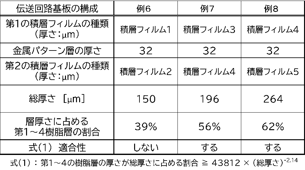
ポリイミド層の厚さとポリイミド層に塗工する液状組成物1の塗工層の厚さとを、表3に示すとおり変化させる以外は例1と同様の操作を行って、Fポリマーを含む第1の樹脂層、ポリイミド層、Fポリマーを含む第2の樹脂層がこの順に積層された積層フィルム6~9を得る。なお、積層フィルム6及び8は式(11)で表される式を満たし、積層フィルム7及び9は下式(11)で表される式を満たさない。

Claims (14)
- 第1の積層フィルム、金属パターン層、及び第2の積層フィルムがこの順に積層され、前記第1の積層フィルムは、テトラフルオロエチレン系ポリマーを含む第1の樹脂層、ポリイミド層、テトラフルオロエチレン系ポリマーを含む第2の樹脂層がこの順に積層されており、
前記第2の積層フィルムは、テトラフルオロエチレン系ポリマーを含む第3の樹脂層、ポリイミド層、テトラフルオロエチレン系ポリマーを含む第4の樹脂層がこの順に積層されており、
前記第1の積層フィルム、前記金属パターン層及び前記第2の積層フィルムの総厚さが150μm超400μm以下であり、
前記総厚さを厚さSとし、前記第3の樹脂層及び前記第4の樹脂層の総厚さが厚さSに占める割合を割合Fとすると、厚さSと割合Fとが下式(1)で表される式を満たす、伝送回路基板。
割合F ≧ 43872×(厚さS)-2.14 ・・・(1) - 前記テトラフルオロエチレン系ポリマーが、ペルフルオロ(アルキルビニルエーテル)に基づく単位を含む、請求項1に記載の伝送回路基板。
- さらに、片側又は両側の最外層に金属層を有する、請求項1に記載の伝送回路基板。
- 第1の積層フィルム、金属パターン層、及び第2の積層フィルムがこの順に積層され、前記第1の積層フィルムは、テトラフルオロエチレン系ポリマーを含む第1の樹脂層、ポリイミド層、テトラフルオロエチレン系ポリマーを含む第2の樹脂層がこの順に積層されており、
前記第2の積層フィルムは、テトラフルオロエチレン系ポリマーを含む第3の樹脂層、ポリイミド層、テトラフルオロエチレン系ポリマーを含む第4の樹脂層がこの順に積層されており、
前記第1の積層フィルム、前記金属パターン層及び前記第2の積層フィルムの総厚さに対する、前記第1の樹脂層、前記第2の樹脂層、前記第3の樹脂層及び前記第4の樹脂層の合計厚さの割合が50%超75%以下であり、
前記総厚さが150μm超400μm以下である、伝送回路基板。 - 前記テトラフルオロエチレン系ポリマーが、ペルフルオロ(アルキルビニルエーテル)に基づく単位を含む、請求項4に記載の伝送回路基板。
- さらに、片側又は両側の最外層に金属層を有する、請求項4に記載の伝送回路基板。
- テトラフルオロエチレン系ポリマーを含む第1の樹脂層、ポリイミド層、テトラフルオロエチレン系ポリマーを含む第2の樹脂層がこの順に積層され、
前記第1の樹脂層、前記ポリイミド層及び前記第2の樹脂層の総厚さが50μm超200μm以下であり、
前記総厚さをSaとし、前記第1の樹脂層及び前記第2の樹脂層の総厚さが厚さと厚さSaに占める割合を割合Faとすると、厚さSaと割合Faとが下式(11)で表される式を満たす、積層フィルム。
割合Fa ≧ 43872×(厚さSa)-2.14 ・・・(11) - 前記第1の樹脂層及び前記第2の樹脂層の厚さが、それぞれ20μm超100μm以下であり、かつ、前記ポリイミド層の厚さが、50μm以下である、請求項7に記載の積層フィルム。
- 前記テトラフルオロエチレン系ポリマーが、ペルフルオロ(アルキルビニルエーテル)に基づく単位を含む、請求項7に記載の積層フィルム。
- 前記テトラフルオロエチレン系ポリマーが、カルボニル基含有基を有する、熱溶融性のテトラフルオロエチレン系ポリマーである、請求項7に記載の積層フィルム。
- テトラフルオロエチレン系ポリマーを含む第1の樹脂層、ポリイミド層、テトラフルオロエチレン系ポリマーを含む第2の樹脂層がこの順に積層され、
前記第1の樹脂層、前記ポリイミド層及び前記第2の樹脂層の総厚さが50μm超200μm以下であり、前記総厚さに対する、前記第1の樹脂層及び前記第2の樹脂層の合計厚さの割合が50%超75%以下である、積層フィルム。 - 前記第1の樹脂層及び前記第2の樹脂層の厚さが、それぞれ20μm超100μm以下であり、かつ、前記ポリイミド層の厚さが、50μm以下である、請求項11に記載の積層フィルム。
- 前記テトラフルオロエチレン系ポリマーが、ペルフルオロ(アルキルビニルエーテル)に基づく単位を含む、請求項11に記載の積層フィルム。
- 前記テトラフルオロエチレン系ポリマーが、カルボニル基含有基を有する、熱溶融性のテトラフルオロエチレン系ポリマーである、請求項11に記載の積層フィルム。
Priority Applications (3)
| Application Number | Priority Date | Filing Date | Title |
|---|---|---|---|
| JP2025513934A JPWO2024214645A1 (ja) | 2023-04-10 | 2024-04-05 | |
| CN202480023590.1A CN120982215A (zh) | 2023-04-10 | 2024-04-05 | 传输电路基板和层叠膜 |
| KR1020257023643A KR20260002596A (ko) | 2023-04-10 | 2024-04-05 | 전송 회로 기판 및 적층 필름 |
Applications Claiming Priority (2)
| Application Number | Priority Date | Filing Date | Title |
|---|---|---|---|
| JP2023-063254 | 2023-04-10 | ||
| JP2023063254 | 2023-04-10 |
Publications (1)
| Publication Number | Publication Date |
|---|---|
| WO2024214645A1 true WO2024214645A1 (ja) | 2024-10-17 |
Family
ID=93059398
Family Applications (1)
| Application Number | Title | Priority Date | Filing Date |
|---|---|---|---|
| PCT/JP2024/014066 Ceased WO2024214645A1 (ja) | 2023-04-10 | 2024-04-05 | 伝送回路基板及び積層フィルム |
Country Status (4)
| Country | Link |
|---|---|
| JP (1) | JPWO2024214645A1 (ja) |
| KR (1) | KR20260002596A (ja) |
| CN (1) | CN120982215A (ja) |
| WO (1) | WO2024214645A1 (ja) |
Citations (2)
| Publication number | Priority date | Publication date | Assignee | Title |
|---|---|---|---|---|
| WO2015080260A1 (ja) * | 2013-11-29 | 2015-06-04 | 旭硝子株式会社 | 接着フィルム及びフレキシブル金属積層板 |
| WO2021039735A1 (ja) * | 2019-08-27 | 2021-03-04 | Agc株式会社 | フィルム、フィルムの製造方法、金属張積層体、及び被覆金属導体 |
-
2024
- 2024-04-05 KR KR1020257023643A patent/KR20260002596A/ko active Pending
- 2024-04-05 WO PCT/JP2024/014066 patent/WO2024214645A1/ja not_active Ceased
- 2024-04-05 CN CN202480023590.1A patent/CN120982215A/zh active Pending
- 2024-04-05 JP JP2025513934A patent/JPWO2024214645A1/ja active Pending
Patent Citations (2)
| Publication number | Priority date | Publication date | Assignee | Title |
|---|---|---|---|---|
| WO2015080260A1 (ja) * | 2013-11-29 | 2015-06-04 | 旭硝子株式会社 | 接着フィルム及びフレキシブル金属積層板 |
| WO2021039735A1 (ja) * | 2019-08-27 | 2021-03-04 | Agc株式会社 | フィルム、フィルムの製造方法、金属張積層体、及び被覆金属導体 |
Also Published As
| Publication number | Publication date |
|---|---|
| KR20260002596A (ko) | 2026-01-06 |
| CN120982215A (zh) | 2025-11-18 |
| JPWO2024214645A1 (ja) | 2024-10-17 |
Similar Documents
| Publication | Publication Date | Title |
|---|---|---|
| JP7283208B2 (ja) | パウダー分散液、積層体の製造方法、積層体及びプリント基板の製造方法 | |
| TWI910105B (zh) | 積層體、印刷基板之製造方法、印刷基板及天線 | |
| US12351684B2 (en) | Polyimide resin precursor, polyimide resin, metal-clad laminated board, laminate, and flexible printed wiring board | |
| WO2021075504A1 (ja) | 非水系分散液及び積層体の製造方法 | |
| JP7484917B2 (ja) | 積層体の製造方法及び積層体 | |
| JP7476721B2 (ja) | 積層板の製造方法及び積層板 | |
| JP2015106629A (ja) | 高周波回路用プリント配線基板 | |
| US12119142B2 (en) | Film, method for producing film, metal-clad laminate, and coated metal conductor | |
| JP7143793B2 (ja) | 積層体及び積層体の製造方法 | |
| JP7740231B2 (ja) | 多層フィルム、その製造方法、金属張積層体及びプリント配線基板の製造方法 | |
| KR20260002596A (ko) | 전송 회로 기판 및 적층 필름 | |
| JP2025049784A (ja) | 金属張積層板及びその製造方法 | |
| CN115003506B (zh) | 多层膜及其制造方法 | |
| TW202344597A (zh) | 分散組成物、氟系樹脂膜、覆金屬積層板及其製造方法 | |
| WO2014106930A1 (ja) | 高周波回路用基板 | |
| JP7771961B2 (ja) | 積層フィルムの製造方法及び積層フィルム | |
| WO2024253037A1 (ja) | 樹脂付金属箔 | |
| JP4850560B2 (ja) | フレキシブルプリント配線用基板 | |
| JP2026040883A (ja) | 液状組成物、ポリマー層付基材の製造方法及びポリマー層付基材 | |
| WO2023153485A1 (ja) | 組成物、フィルム、積層体及び積層体の製造方法 | |
| JP2020152055A (ja) | 積層体、プリント基板の製造方法、プリント基板及びアンテナ |
Legal Events
| Date | Code | Title | Description |
|---|---|---|---|
| 121 | Ep: the epo has been informed by wipo that ep was designated in this application |
Ref document number: 24788669 Country of ref document: EP Kind code of ref document: A1 |
|
| ENP | Entry into the national phase |
Ref document number: 2025513934 Country of ref document: JP Kind code of ref document: A |
|
| WWE | Wipo information: entry into national phase |
Ref document number: 2025513934 Country of ref document: JP |
|
| NENP | Non-entry into the national phase |
Ref country code: DE |
|
| 122 | Ep: pct application non-entry in european phase |
Ref document number: 24788669 Country of ref document: EP Kind code of ref document: A1 |