WO2024214583A1 - 検出装置 - Google Patents
検出装置 Download PDFInfo
- Publication number
- WO2024214583A1 WO2024214583A1 PCT/JP2024/013415 JP2024013415W WO2024214583A1 WO 2024214583 A1 WO2024214583 A1 WO 2024214583A1 JP 2024013415 W JP2024013415 W JP 2024013415W WO 2024214583 A1 WO2024214583 A1 WO 2024214583A1
- Authority
- WO
- WIPO (PCT)
- Prior art keywords
- substrate
- wiring
- insulating layer
- detection device
- photodiode
- Prior art date
- Legal status (The legal status is an assumption and is not a legal conclusion. Google has not performed a legal analysis and makes no representation as to the accuracy of the status listed.)
- Ceased
Links
Images


Classifications
-
- H—ELECTRICITY
- H10—SEMICONDUCTOR DEVICES; ELECTRIC SOLID-STATE DEVICES NOT OTHERWISE PROVIDED FOR
- H10K—ORGANIC ELECTRIC SOLID-STATE DEVICES
- H10K39/00—Integrated devices, or assemblies of multiple devices, comprising at least one organic radiation-sensitive element covered by group H10K30/00
- H10K39/30—Devices controlled by radiation
- H10K39/32—Organic image sensors
-
- A—HUMAN NECESSITIES
- A61—MEDICAL OR VETERINARY SCIENCE; HYGIENE
- A61B—DIAGNOSIS; SURGERY; IDENTIFICATION
- A61B5/00—Measuring for diagnostic purposes; Identification of persons
- A61B5/117—Identification of persons
- A61B5/1171—Identification of persons based on the shapes or appearances of their bodies or parts thereof
- A61B5/1172—Identification of persons based on the shapes or appearances of their bodies or parts thereof using fingerprinting
-
- A—HUMAN NECESSITIES
- A61—MEDICAL OR VETERINARY SCIENCE; HYGIENE
- A61B—DIAGNOSIS; SURGERY; IDENTIFICATION
- A61B5/00—Measuring for diagnostic purposes; Identification of persons
- A61B5/48—Other medical applications
- A61B5/4887—Locating particular structures in or on the body
- A61B5/489—Blood vessels
-
- A—HUMAN NECESSITIES
- A61—MEDICAL OR VETERINARY SCIENCE; HYGIENE
- A61B—DIAGNOSIS; SURGERY; IDENTIFICATION
- A61B5/00—Measuring for diagnostic purposes; Identification of persons
- A61B5/68—Arrangements of detecting, measuring or recording means, e.g. sensors, in relation to patient
- A61B5/6801—Arrangements of detecting, measuring or recording means, e.g. sensors, in relation to patient specially adapted to be attached to or worn on the body surface
- A61B5/6813—Specially adapted to be attached to a specific body part
- A61B5/6825—Hand
- A61B5/6826—Finger
-
- G—PHYSICS
- G06—COMPUTING OR CALCULATING; COUNTING
- G06V—IMAGE OR VIDEO RECOGNITION OR UNDERSTANDING
- G06V40/00—Recognition of biometric, human-related or animal-related patterns in image or video data
- G06V40/10—Human or animal bodies, e.g. vehicle occupants or pedestrians; Body parts, e.g. hands
- G06V40/12—Fingerprints or palmprints
- G06V40/13—Sensors therefor
- G06V40/1318—Sensors therefor using electro-optical elements or layers, e.g. electroluminescent sensing
-
- G—PHYSICS
- G06—COMPUTING OR CALCULATING; COUNTING
- G06V—IMAGE OR VIDEO RECOGNITION OR UNDERSTANDING
- G06V40/00—Recognition of biometric, human-related or animal-related patterns in image or video data
- G06V40/40—Spoof detection, e.g. liveness detection
- G06V40/45—Detection of the body part being alive
-
- H—ELECTRICITY
- H10—SEMICONDUCTOR DEVICES; ELECTRIC SOLID-STATE DEVICES NOT OTHERWISE PROVIDED FOR
- H10K—ORGANIC ELECTRIC SOLID-STATE DEVICES
- H10K30/00—Organic devices sensitive to infrared radiation, light, electromagnetic radiation of shorter wavelength or corpuscular radiation
- H10K30/60—Organic devices sensitive to infrared radiation, light, electromagnetic radiation of shorter wavelength or corpuscular radiation in which radiation controls flow of current through the devices, e.g. photoresistors
-
- H—ELECTRICITY
- H10—SEMICONDUCTOR DEVICES; ELECTRIC SOLID-STATE DEVICES NOT OTHERWISE PROVIDED FOR
- H10K—ORGANIC ELECTRIC SOLID-STATE DEVICES
- H10K30/00—Organic devices sensitive to infrared radiation, light, electromagnetic radiation of shorter wavelength or corpuscular radiation
- H10K30/80—Constructional details
- H10K30/88—Passivation; Containers; Encapsulations
-
- A—HUMAN NECESSITIES
- A61—MEDICAL OR VETERINARY SCIENCE; HYGIENE
- A61B—DIAGNOSIS; SURGERY; IDENTIFICATION
- A61B2562/00—Details of sensors; Constructional details of sensor housings or probes; Accessories for sensors
- A61B2562/16—Details of sensor housings or probes; Details of structural supports for sensors
- A61B2562/164—Details of sensor housings or probes; Details of structural supports for sensors the sensor is mounted in or on a conformable substrate or carrier
-
- A—HUMAN NECESSITIES
- A61—MEDICAL OR VETERINARY SCIENCE; HYGIENE
- A61B—DIAGNOSIS; SURGERY; IDENTIFICATION
- A61B2562/00—Details of sensors; Constructional details of sensor housings or probes; Accessories for sensors
- A61B2562/16—Details of sensor housings or probes; Details of structural supports for sensors
- A61B2562/166—Details of sensor housings or probes; Details of structural supports for sensors the sensor is mounted on a specially adapted printed circuit board
-
- G—PHYSICS
- G06—COMPUTING OR CALCULATING; COUNTING
- G06V—IMAGE OR VIDEO RECOGNITION OR UNDERSTANDING
- G06V40/00—Recognition of biometric, human-related or animal-related patterns in image or video data
- G06V40/10—Human or animal bodies, e.g. vehicle occupants or pedestrians; Body parts, e.g. hands
- G06V40/14—Vascular patterns
- G06V40/145—Sensors therefor
Definitions
- the present invention relates to a detection device.
- Optical sensors capable of detecting fingerprint patterns and vein patterns are known (for example, Patent Document 1).
- sensors having multiple photodiodes in which an organic semiconductor material is used as the active layer are known.
- the organic semiconductor material is disposed between a lower electrode and an upper electrode, and a signal line for outputting a detection signal to a detection circuit is electrically connected to the lower electrode of the photodiode.
- the object of the present invention is to provide a detection device that can reduce stress concentration in wiring at stepped areas and suppress wiring cracks.
- a detection device includes a photodiode having a lower electrode, a lower buffer layer, an active layer, an upper buffer layer, and an upper electrode, a first substrate, a first insulating layer between the first substrate and the photodiode, a second substrate covering at least the photodiode and having an area smaller than that of the first substrate so as to have the photodiode between the first substrate and the first insulating layer, an active region in which the active layer of the photodiode is located, a connection region in which a connection portion provided at an end of the first substrate is located, and a second insulating layer between the second substrate and the photodiode.
- the peripheral region includes a peripheral region between the active region and the connection region, a sealing film that seals the active region and the peripheral region, the lower electrode, and a first wiring that connects the connection portion
- the peripheral region includes a first portion having the first insulating layer, the sealing film, the second insulating layer, and the second substrate on the first substrate, and a second portion in which at least one of the sealing film, the second insulating layer, or the second substrate is cut out from the first portion, and the boundary between the first portion and the second portion is along a first direction from the connection region toward the active region, and the boundary line intersects with the first wiring.
- a detection device includes an organic photodiode having a lower electrode, a lower buffer layer, an active layer, an upper buffer layer, and an upper electrode, a first substrate, a first insulating layer between the first substrate and the photodiode, a second substrate covering at least the photodiode and having an area smaller than that of the first substrate so as to have the photodiode between the first substrate, a second insulating layer between the second substrate and the photodiode, an active region in which the active layer of the photodiode is located, a connection region in which a connection portion provided at an end of the first substrate is disposed, a peripheral region between the active region and the connection region, and a substrate sealing the active region and the peripheral region.
- the peripheral region has a first portion having the first insulating layer, the sealing film, the second insulating layer, and the second substrate on the first substrate, and a second portion having the first insulating layer on the first substrate, and the first wiring intersects with the boundary between the first portion and the second portion along a second direction intersecting with a first direction from the connection region toward the active region, and a flexible printed circuit board is connected to the connection region, and a protective film covering the second substrate extends to the peripheral region and the connection region so as to overlap the entire surface of the active region, and a part of the flexible printed circuit board is sandwiched between the protective film and the second substrate.
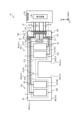
- FIG. 1 is a schematic diagram showing an example of the external appearance of a detection device according to a first embodiment when a finger is placed inside the detection device as viewed from the side of a housing.
- FIG. 2 is a schematic cross-sectional view taken along line II-II' of FIG.
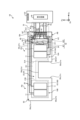
- FIG. 3 is a development view showing an example of the optical sensor of the detection device shown in FIG.
- FIG. 4 is a diagram showing an example of the configuration of the first optical sensor and the second optical sensor shown in FIG.
- FIG. 5 is a schematic cross-sectional view showing an example of a laminated structure of the optical sensor taken along the line VV' shown in FIG. FIG.
- FIG. 6 is a schematic cross-sectional view showing an example of a laminated structure of the optical sensor taken along the line VI-VI′ shown in FIG.
- FIG. 7 is a schematic cross-sectional view showing an example of a laminated structure of the optical sensor taken along the line VII-VII′ shown in FIG.
- FIG. 8 is a schematic cross-sectional view showing an example of a laminated structure of the optical sensor taken along the line VIII-VIII′ shown in FIG.
- FIG. 9 is a diagram illustrating an example of the configuration of a first optical sensor and a second optical sensor according to a comparative example.
- FIG. 10 is a schematic cross-sectional view showing an example of a stacked configuration of the optical sensor shown in FIG. FIG.
- FIG. 11 is a schematic cross-sectional view showing a state in which the optical sensor shown in FIG. 9 is bent in the third direction.
- FIG. 12 is a diagram illustrating an example of the configuration of the first optical sensor and the second optical sensor according to the second embodiment.
- FIG. 13 is a schematic cross-sectional view showing an example of a laminated structure of the optical sensor taken along the line XIII-XIII′ shown in FIG.
- FIG. 14 is a schematic cross-sectional view illustrating an example of a stacked configuration of an optical sensor according to the third embodiment.
- FIG. 15 is a diagram illustrating an example of the configuration of a first optical sensor and a second optical sensor according to the fourth embodiment.
- FIG. 16 is a diagram illustrating an example of the configuration of a first optical sensor and a second optical sensor according to the fifth embodiment.
- FIG. 17 is a schematic cross-sectional view showing an example of a stacked configuration of the optical sensor shown in FIG.
- the term "on top” is used, unless otherwise specified, to include both a case in which another structure is placed directly on top of a structure so as to be in contact with the structure, and a case in which another structure is placed above a structure via yet another structure.
- Fig. 1 is a schematic diagram showing an external appearance example of a detection device according to embodiment 1 when a finger is placed inside the detection device when viewed from the side of a housing.
- Fig. 2 is a schematic cross-sectional view taken along II-II' cross section shown in Fig. 1.
- Fig. 3 is a development view showing an example of development of an optical sensor of the detection device shown in Fig. 1.
- Fig. 4 is a configuration diagram showing an example of the configuration of a first optical sensor and a second optical sensor shown in Fig. 3.
- Fig. 5 is a schematic cross-sectional view showing an example of a stacked configuration of an optical sensor taken along V-V' cross section shown in Fig. 4.
- Fig. 6 is a schematic cross-sectional view showing an example of a stacked configuration of an optical sensor taken along VI-VI' cross section shown in Fig. 4.
- the detection device 1 shown in FIG. 1 is a ring-shaped device that can be attached and detached to the human body, and is worn on a finger Fg of the human body.
- the finger Fg includes the thumb, index finger, middle finger, ring finger, little finger, etc.
- the human body is the person to be authenticated, whose identity is verified by the detection device 1.
- the detection device 1 can detect biometric information about a living body from the finger Fg on which it is worn.
- the finger Fg is an example of a measurement target.
- the measurement target is a living body or a part of a living body, and is the measurement target.
- the detection device 1 is made into a ring or wristband, making it easy for the user to carry. In the following description, it is assumed that the detection device 1 is used as a ring.
- the detection device 1 includes a housing 200, a light source 60, a first optical sensor 10A, and a second optical sensor 10B.
- the detection device 1 includes a battery (not shown) inside the housing 200 and is a device that operates using battery power.
- the housing 200 is formed in a ring shape (annular shape) that can be attached to the finger Fg, and is a wearing member that is attached to a living body.
- the housing 200 includes a sealing film 210 and an exterior part 220.
- the housing 200 is formed in a ring shape by integrating the sealing film 210 and the exterior part 220.
- the sealing film 210 houses the light source 60, the first optical sensor 10A, the second optical sensor 10B, etc. inside.
- the sealing film 210 is formed in a ring shape from a housing material such as, for example, a transparent synthetic resin or silicone.
- the exterior part 220 has a surface of the housing 200 that covers the outer peripheral surface 210A of the sealing film 210.
- the exterior part 220 is formed in a ring shape from, for example, a material such as a metal or a non-transparent synthetic resin.
- the housing 200 houses the flexible printed circuit board 70 on which the light source 60, the first optical sensor 10A, the second optical sensor 10B, etc. are mounted inside the sealing film 210.
- the flexible printed circuit board 70 is housed inside the housing 200, for example, by forming the housing 200 in a ring shape in a mold and filling the surrounding area with a filling material.
- the flexible printed circuit board 70 is formed in a deformable belt shape, and is formed into a ring shape by connecting one end 71 and the other end 72.
- the flexible printed circuit board 70 has a first mounting area 73 and a second mounting area 74.
- the first mounting area 73 is an area where the light source 60 and the like are mounted.
- the second mounting area 74 is an area where the control circuit 122, the power supply circuit 123, and the like are mounted.
- the first board 21 is mounted on the flexible printed circuit board 70 so as to straddle the vicinity of the light source 60 in the first mounting area 73.
- the second board 50 is provided on the first board 21.
- the flexible printed circuit board 70 electrically connects the light source 60, the first optical sensor 10A, the second optical sensor 10B, and the like to the control circuit 122.
- the first optical sensor 10A and the second optical sensor 10B are arranged so as to sandwich the light source 60 in the circumferential direction 200C. That is, the detection device 1 is arranged in the circumferential direction 200C with the first optical sensor 10A, the light source 60, and the second optical sensor 10B in that order.
- the first optical sensor 10A and the second optical sensor 10B are arranged so as to sandwich the light source 60 in the circumferential direction 200C, so that the light emitted by the light source 60 can be detected over a wide range of the housing 200.
- the first substrate 21 is an insulating substrate, and is formed in a strip shape from, for example, PET (Poly Ethylene Terephthalate), which is a film-like synthetic resin.
- the first substrate 21 is a deformable substrate on which the first optical sensor 10A and the second optical sensor 10B are mounted.
- the first substrate 21 can be curved in the third direction Dz.
- the first substrate 21 is attached to the flexible printed circuit board 70, and positions the first optical sensor 10A and the second optical sensor 10B on both sides of the light source 60 in the circumferential direction 200C of the housing 200.
- the first substrate 21 has a first region 21A on which the first optical sensor 10A is mounted, and a second region 21B on which the second optical sensor 10B is mounted.
- the first substrate 21 is formed as a single substrate having the first region 21A and the second region 21B.
- the second substrate 50 is an insulating substrate, and is formed in a strip shape from, for example, PET (Poly Ethylene Terephthalate), a film-like synthetic resin.
- the second substrate 50 covers the sealing film 210, and is a deformable substrate.
- the second substrate 50 can be curved in the third direction Dz.
- the flexible printed circuit board 70 is housed inside the housing 200 so that the surface on which the first optical sensor 10A, the second optical sensor 10B, and the light source 60 are mounted faces the inner peripheral surface 200B of the housing 200. If the flexible printed circuit board 70 is translucent, the first optical sensor 10A, the second optical sensor 10B, and the light source 60 may be mounted on the back surface opposite the front surface. In this case, the light source 60 may be positioned so that it emits light toward the flexible printed circuit board 70 and the light that has passed through the flexible printed circuit board 70 is emitted toward the outside of the housing 200.
- the light source 60 is provided inside the sealing film 210 of the housing 200, and is configured to be able to irradiate light toward a detection object such as a finger Fg attached to the ring-shaped housing 200.
- a detection object such as a finger Fg attached to the ring-shaped housing 200.
- an inorganic LED Light Emitting Diode
- an organic EL Organic Light Emitting Diode
- the light source 60 irradiates light of a predetermined wavelength.
- the light source 60 has multiple light sources so as to be able to irradiate near-infrared light, red light, and green light.
- the light emitted from the light source 60 is reflected by the surface of the object to be detected, such as a finger Fg, and enters the first optical sensor 10A and the second optical sensor 10B.
- the light emitted from the light source 60 may be reflected inside the finger Fg or pass through the finger Fg and enter the first optical sensor 10A and the second optical sensor 10B.
- Information about a living body includes, for example, the pulse wave, pulse, and blood vessel image of the finger or palm.
- the detection device 1 may be configured as a fingerprint detection device that detects fingerprints, or a vein detection device that detects blood vessel patterns such as veins.
- the first optical sensor 10A and the second optical sensor 10B each detect light emitted by the light source 60 and reflected by the finger Fg, etc., and light that is directly incident.
- the first optical sensor 10A and the second optical sensor 10B are organic photodiodes (OPDs).
- OPDs organic photodiodes
- the first optical sensor 10A is provided on the housing 200 so as to be adjacent to one end 61 of the light source 60 in the circumferential direction 200C of the housing 200.
- the second optical sensor 10B is provided on the housing 200 so as to be adjacent to the other end 62 of the light source 60 in the circumferential direction 200C of the housing 200.
- the first optical sensor 10A and the second optical sensor 10B have a photodiode PD (see FIG. 4), which is an organic photodiode.
- PD photodiode
- Each of the first optical sensor 10A and the second optical sensor 10B has two lower electrodes 11 arranged along the circumferential direction 200C.
- the first optical sensor 10A and the second optical sensor 10B are mounted on a single first substrate 21 and are electrically connected to the flexible printed circuit board 70 via the first substrate 21.
- the first substrate 21 has a cutout portion 22 (see FIG. 4) between the first optical sensor 10A and the second optical sensor 10B in the circumferential direction 200C of the housing 200.
- the first direction Dx is a direction in a plane parallel to the first substrate 21 and is the same direction as the circumferential direction 200C.
- the second direction Dy is a direction in a plane parallel to the first substrate 21 and is a direction perpendicular to the first direction Dx.
- the second direction Dy may intersect the first direction Dx without being perpendicular thereto.
- the third direction Dz is a direction perpendicular to the first direction Dx and the second direction Dy.
- the third direction Dz is the normal direction of the first substrate 21.
- plane view refers to the positional relationship when viewed from a direction perpendicular to the first substrate 21.
- the first optical sensor 10A is configured by stacking two lower electrodes 11 aligned in the first direction Dx and one upper electrode 15A.
- the second optical sensor 10B is configured by stacking two lower electrodes 11 aligned in the first direction Dx and one upper electrode 15B.
- the upper electrode 15 includes the upper electrode 15A of the first optical sensor 10A and the upper electrode 15B of the second optical sensor 10B. Each of the upper electrode 15A and the upper electrode 15B covers the two lower electrodes 11 in a plan view.
- the upper electrode 15A and the upper electrode 15B are electrically connected by an electrode connection portion 151.
- the upper electrode 15A, the upper electrode 15B, and the electrode connection portion 151 are integrally formed.
- the first substrate 21 has a power electrode 211 extending along the second direction Dy.
- the power electrode 211 is electrically connected to a connection portion 212 (terminal portion) of the first substrate 21 via a conductive material 213, and a sensor power signal is supplied from the power circuit 123 (see FIG. 3) via the connection portion 212.
- the upper electrode 15 is electrically connected to the power electrode 211 by the conductive material 213.
- the conductive material 213 is provided on the first substrate 21 so as to straddle the upper electrode 15 and the power electrode 211, and is formed of a material having electrical conductivity. As a result, the upper electrode 15 is supplied with a sensor power signal from the power circuit 123 via the power electrode 211.
- the multiple first wirings 26 of the first substrate 21 are connected to a detection circuit 48 of the control circuit 122 via multiple signal lines SL of the flexible printed circuit board 70.
- the detection circuit 48 is electrically connected to the lower electrodes 11 of the first optical sensor 10A and the second optical sensor 10B via multiple signal lines SL.
- the detection circuit 48 may be formed as a circuit separate from the control circuit 122.
- the first wiring 26 is formed, for example, of a metal wiring, and is formed of a material having better conductivity than the lower electrode 11 of the photodiode PD.
- the first wiring 26 is formed, for example, of a conductive material having translucency, such as ITO (Indium Tin Oxide).
- the first wiring 26 is provided in a layer between the first substrate 21 and the photodiode PD in the third direction Dz.
- the first wiring 26 is electrically connected to the lower electrode 11 and the connection portion 212 on the first substrate 21.
- the first wiring 26 may be formed, for example, in the same layer as the lower electrode 11, or may be formed of metal.
- the second wiring 260 is electrically connected to the power electrode 211 by the conductive material 213.
- the second wiring 260 is formed of, for example, a metal wiring, and is formed of a material having electrical conductivity.
- the second wiring 260 is formed of a material having better electrical conductivity than the upper electrode 15.
- the second wiring 260 is provided in a layer between the first substrate 21 and the photodiode PD in the third direction Dz.
- the second wiring 260 is electrically connected to the upper electrode 15 and the connection portion 212.
- the second wiring 260 may be formed, for example, in the same layer as the upper electrode 15, or may be formed of a metal.
- the second wiring 260 may also be a shield layer.
- the control circuit 122 is a circuit that supplies control signals to the multiple photodiodes PD to control the detection operation.
- the multiple photodiodes PD each output an electrical signal corresponding to the light irradiated thereon as a detection signal Vdet to the detection circuit 48.
- the second wiring 260 is also connected to the control circuit 122 via a wiring 261 that supplies a power supply voltage to the second wiring 260.
- the detection signals Vdet of the multiple photodiodes PD are output to the detection circuit 48 in a time-division sequential manner.
- the multiple signal lines SL are electrically connected to the detection circuit 48 in a time-division sequential manner.
- the detection device 1 detects information about the object to be detected based on the detection signals Vdet from the multiple photodiodes PD.
- the first substrate 21 has a first side 21a, a second side 21b, a third side 21c, a fourth side 21d, a fifth side 21e, a sixth side 21f, and a seventh side 21n.
- the second substrate 50 has a first side 50a, a second side 50b, a third side 50c, a fourth side 50d, a fifth side 50e, a sixth side 50f, a seventh side 50g, an eighth side 50h, a ninth side 50i, a tenth side 50j, an eleventh side 50k and a twelfth side 50n.
- the first side 21a and the first side 50a are parallel planes of equal length and overlap.
- the second side 21b and the second side 50b are parallel planes of equal length and overlap.
- the third side 21c and the third side 50c are parallel planes of equal length and overlap.
- the fourth side 21d and the fourth side 50d are parallel planes of equal length, and overlap.
- the fifth side 21e and the fifth side 50e are parallel planes of equal length and overlap.
- the sixth side 50f and the sixth side 21f are parallel, but the sixth side 50f is shorter in length than the sixth side 21f.
- the twelfth side 50n and the seventh side 21n are parallel, but the twelfth side 50n is shorter in length than the seventh side 21n.
- the first substrate 21 does not have any side surfaces in the portions that overlap with the seventh side 50g, the eighth side 50h, the ninth side 50i, the tenth side 50j, and the eleventh side 50k.
- the second substrate 50 which covers the photodiode PD and has a smaller area than the first substrate 21, is provided on the first substrate 21.
- the first optical sensor 10A has a first substrate 21 (first region 21A), a photodiode PD, and a second substrate 50 facing the first substrate 21.
- the first optical sensor 10A further has a first insulating layer 27 and a second insulating layer 270.
- the first insulating layer 27 is provided on the first substrate 21.
- the first insulating layer 27 is disposed between the first substrate 21 and the photodiode PD.
- the second insulating layer 270 is provided on the photodiode PD.
- the second insulating layer 270 is disposed between the second substrate 50 and the photodiode PD.
- the first insulating layer 27 and the second insulating layer 270 may be inorganic insulating films or organic insulating films.
- the photodiode PD is provided on the first insulating layer 27.
- the photodiode PD has a lower electrode 11, a lower buffer layer 12, an active layer 13, an upper buffer layer 14, and an upper electrode 15 (15A).
- the photodiode PD is stacked in the following order in the third direction Dz perpendicular to the first substrate 21: the lower electrode 11, the lower buffer layer 12 (hole transport layer), the active layer 13, the upper buffer layer 14 (electron transport layer), and the upper electrode 15.
- the lower electrode 11 is the anode electrode of the photodiode PD and is formed of a conductive material having light transmission, such as ITO (Indium Tin Oxide).
- ITO Indium Tin Oxide
- the characteristics (e.g., voltage-current characteristics and resistance value) of the active layer 13 change depending on the light irradiated thereto.
- An organic material is used as the material of the active layer 13.
- the active layer 13 is a bulk heterostructure in which a p-type organic semiconductor and an n-type fullerene derivative (PCBM), which is an n-type organic semiconductor, are mixed.
- PCBM n-type fullerene derivative
- low molecular weight organic materials such as C60 (fullerene), PCBM (phenyl C61-butyric acid methyl ester), CuPc (copper phthalocyanine), F16CuPc (fluorinated copper phthalocyanine), rubrene (5,6,11,12-tetraphenyltetracene), and PDI (perylene derivative) can be used as the active layer 13.
- C60 fulllerene
- PCBM phenyl C61-butyric acid methyl ester
- CuPc copper phthalocyanine
- F16CuPc fluorinated copper phthalocyanine
- rubrene 5,6,11,12-tetraphenyltetracene
- PDI perylene derivative
- the active layer 13 can be formed by a deposition type (dry process) using these low molecular weight organic materials.
- the active layer 13 may be, for example, a laminated film of CuPc and F16CuPc, or a laminated film of rubrene and C60.
- the active layer 13 can also be formed by a coating type (wet process).
- the active layer 13 is made of a material that combines the above-mentioned low molecular weight organic material and a polymer organic material.
- the polymer organic material for example, P3HT (poly(3-hexylthiophene)), F8BT (F8-alt-benzothiadiazole), etc. can be used.
- the active layer 13 can be a film in which P3HT and PCBM are mixed, or a film in which F8BT and PDI are mixed.
- the lower buffer layer 12 is a hole transport layer.
- the upper buffer layer 14 is an electron transport layer.
- the lower buffer layer 12 and the upper buffer layer 14 are provided to facilitate the holes and electrons generated in the active layer 13 reaching the lower electrode 11 or the upper electrode 15.
- the lower buffer layer 12 (hole transport layer) is directly on top of the lower electrode 11 and is also provided in the region between adjacent lower electrodes 11.
- the active layer 13 is directly on top of the lower buffer layer 12.
- the material of the hole transport layer is a metal oxide layer. Tungsten oxide (WO3), molybdenum oxide, etc. are used as the metal oxide layer.
- the upper buffer layer 14 (electron transport layer) is in direct contact with the active layer 13, and the upper electrode 15 is in direct contact with the upper buffer layer 14.
- the material used for the electron transport layer is ethoxylated polyethyleneimine (PEIE).
- the materials and manufacturing methods of the lower buffer layer 12, active layer 13, and upper buffer layer 14 are merely examples, and other materials and manufacturing methods may be used.
- the lower buffer layer 12 and upper buffer layer 14 are not limited to single-layer films, and may be formed as laminated films including an electron blocking layer and a hole blocking layer.
- the upper electrode 15 is provided on the upper buffer layer 14.
- the upper electrode 15 is a cathode electrode of the photodiode PD, and is formed continuously over the entire first optical sensor 10A and the second optical sensor 10B. In other words, the upper electrode 15 is provided continuously on the multiple photodiodes PD.
- the upper electrode 15 faces the multiple lower electrodes 11, sandwiching the lower buffer layer 12, the active layer 13, and the upper buffer layer 14.
- the upper electrode 15 is formed of a conductive material having translucency, such as ITO or IZO. A part of the end of the upper surface 150 of the upper electrode 15 is electrically connected to the conductive material 213.
- the photodiode PD is well sealed by providing the sealing film 210 on the upper electrode 15, etc.
- the second optical sensor 10B has the lower electrode 11 of the second optical sensor 10B in a second region 21B of the first substrate 21, which is different from the lower electrode 11 of the first optical sensor 10A.
- the lower electrode 11 is covered with a lower buffer layer 12, an active layer 13, an upper buffer layer 14, and an upper electrode 15 (15B).
- the second optical sensor 10B has a first substrate 21 (second region 21B), a photodiode PD, a first insulating layer 27, a second substrate 50 facing the first substrate 21, and a second insulating layer 270.
- the second substrate 50, the photodiode PD, the first insulating layer 27, and the second insulating layer 270 have the same configuration as the photodiode PD and the first insulating layer 27 of the first optical sensor 10A described above. That is, the photodiode PD of the second optical sensor 10B has a lower electrode 11, a lower buffer layer 12, an active layer 13, an upper buffer layer 14, and an upper electrode 15 (15B).
- the first optical sensor 10A and the second optical sensor 10B are organic photodiodes.
- the first substrate 21 has the first region 21A of the first optical sensor 10A and the second region 21B of the second optical sensor 10B, and is formed as a single common substrate.
- the first substrate 21 has a cutout portion 22 formed between the first region 21A of the first optical sensor 10A and the second region 21B of the second optical sensor 10B in the first direction Dx.
- the first substrate 21 has the cutout portion 22 between the first optical sensor 10A and the second optical sensor 10B, and a connecting portion 23 that is in contact with the cutout portion 22 and is between the first optical sensor 10A and the second optical sensor 10B.
- the cutout portion 22 is formed in the first direction Dx with a distance L1 that is longer than the length of the light source 60.
- the cutout portion 22 is formed in the second direction Dy with a distance L2 that is longer than the length of the light source 60 and shorter than the length (width) of the first substrate 21.
- the cutout portion 22 is formed so that the center 22C is equal in distance to each side of the lower electrode 11 of the first optical sensor 10A and the lower electrode 11 of the second optical sensor 10B in the first direction Dx.
- the first substrate 21 is integrally formed by connecting the first optical sensor 10A and the second optical sensor 10B at the connecting portion 23 of the cutout portion 22.
- the lower buffer layer 12, the active layer 13, the upper buffer layer 14, and the electrode connecting portion 151 of the upper electrode 15 are arranged in the connecting portion 23.
- the connecting portion 23 integrally forms the upper electrodes 15 of the first optical sensor 10A and the second optical sensor 10B.
- the cutout portion 22 is formed in a shape that allows the light source 60 to be placed therein.
- the cutout portion 22 is formed in a substantially rectangular shape in a plan view, but may be in a semicircular, triangular, polygonal, or other shape.
- the electrode connecting portion 151 is provided on the connecting portion 23 of the first substrate 21 so as to be stacked on the upper buffer layer 14, the active layer 13, and the lower buffer layer 12.
- the region where the active layer 13 (see FIG. 5) of the photodiode PD is arranged is defined as the active region AA.
- the region closer to the connection portion 212 than the plane connecting the seventh side 50g and the tenth side 50j is defined as the connection region AB.
- the region between the active region AA and the connection region AB is defined as the peripheral region AC.
- One end 71 (see FIG. 3) of the flexible printed circuit board 70 including the signal line SL is electrically connected to the connection region AB by anisotropic conductive resin or the like.
- the peripheral area AC has a first portion 40 having a first insulating layer 27, a sealing film 210, a second insulating layer 270, and a second substrate 50 on the first substrate 21, and a second portion 41 in which at least one of the sealing film 210, the second insulating layer 270, or the second substrate 50 is cut out from the first portion 40.
- the sealing film 210 seals the active area AA and the peripheral area AC.
- the boundary line 42 between the first portion 40 and the second portion 41 along the direction from the connection area AB toward the active area AA is parallel to the first direction Dx, and the direction in which the first wiring 26 extends at the portion intersecting the boundary line 42 is perpendicular to the first direction Dx.
- the boundary line 42 has a first side 421 and a second side 422 that faces the first side 421 in the second direction Dy.
- the first side 421 is provided on the tenth side surface 50j.
- the second side 422 is provided on the eighth side surface 50h.
- the first wiring 26 has a wiring 2A and a wiring 2B.
- the wiring 26A intersects with the first side 421, and the wiring 26B intersects with the second side 422.
- the second wiring 260 intersects with the first side 421 and the second side 422.
- the seventh side 50g, the ninth side 50i, and the eleventh side 50k have steps in the third direction that correspond to the thickness of the second substrate 50, but the first wiring 26 and the second wiring 260 do not intersect. Therefore, when the detection device 1 is bent in the third direction, the stress generated in the steps is less likely to be applied to the first wiring 26 and the second wiring 260.
- FIG. 7 is a schematic cross-sectional view showing an example of the stacking configuration of an optical sensor in the VII-VII' cross section shown in FIG. 4.
- FIG. 8 is a schematic cross-sectional view showing an example of the stacking configuration of an optical sensor in the VIII-VIII' cross section shown in FIG. 4.
- the first portion 40 is formed by stacking the second substrate 50, the first insulating layer 27, the sealing film 210, the first insulating layer 27, and the first substrate 21 in that order.
- the first wiring 26 and the second wiring 260 are provided on the upper surface of the first substrate 21.
- the lower electrode 11 is disposed on the upper surface of the first insulating layer 27.
- the second portion 41 has a first substrate 21, a first insulating layer 27, a first wiring 26, and a second wiring 260.
- the first wiring 26 and the second wiring 260 are provided on the upper surface of the first insulating layer 27.
- the second portion 41 has the first insulating layer 27 on the first substrate 21, and the sealing film 210, the second insulating layer 270, and the second substrate 50 are cut out.
- FIG. 9 is a diagram showing an example of the configuration of a first optical sensor and a second optical sensor according to a comparative example.
- FIG. 10 is a schematic cross-sectional view showing an example of the stacked configuration of the optical sensor shown in FIG. 9.
- FIG. 11 is a schematic cross-sectional view showing the shape of the optical sensor shown in FIG. 9 when bent in the third direction.
- the second substrate 50 has a first side 50a, a second side 50b, a third side 50c, a fourth side 50d, a fifth side 50e, a sixth side 50f, a twelfth side 50n, and a thirteenth side 50t.
- the first side 21a and the first side 50a are parallel planes of equal length and overlap.
- the second side 21b and the second side 50b are parallel planes of equal length and overlap.
- the third side 21c and the third side 50c are parallel planes of equal length and overlap.
- the fourth side 21d and the fourth side 50d are parallel planes of equal length and overlap.
- the fifth side 21e and the fifth side 50e are parallel planes of equal length and overlap.
- the sixth side 50f and the sixth side 21f are parallel, but the sixth side 50f is shorter in length than the sixth side 21f.
- the twelfth side 50n and the seventh side 21n are parallel, but the twelfth side 50n is shorter in length than the seventh side 21n.
- the first substrate 21 does not have a side in the portion that overlaps with the thirteenth side 50t.
- the second substrate 50 which covers the photodiode PD and has a smaller area than the first substrate 21, is provided on the first substrate 21.
- the thirteenth side 50t also includes a boundary line 43 between the first portion 40 and the second portion 41.
- the first wiring 26 intersects with the boundary line 43.
- the area of the second substrate 50 in the upper layer is smaller than the area of the first substrate 21 in the lower layer, so a step AX corresponding to the thickness of the second substrate 50 is created in the third direction of the thirteenth side surface 50t on the flexible printed circuit board 70 side.
- the end of the first substrate 21 facing the flexible printed circuit board 70 bends in the direction in which the force is being applied.
- the area of only the first substrate 21 and the area where the second substrate 50 overlaps the first substrate 21 have different thicknesses, and even when the same bending force is applied, there is a difference in the amount of bending. Due to this difference in the amount of bending, the end of the second substrate 50 facing the flexible printed circuit board 70 is pressed against the surface of the first substrate 21, and stress F is concentrated at the step AX. As a result, a crack may occur in the first wiring 26 that intersects with the step AX.
- the first wiring 26 and the second wiring 260 do not intersect the seventh side 50g, the ninth side 50i, and the eleventh side 50k, where a step corresponding to the thickness of the first substrate 21 occurs.
- the first wiring 26 and the second wiring 260 intersect the first side 421 and the second side 422, when the detection device 1 is bent in the third direction, the first wiring 26 and the second wiring 260 are less likely to be subjected to stress at the first side 421 and the second side 422. As a result, cracks in the first wiring 26 and the second wiring 260 that intersect the first side 421 and the second side 422 are suppressed.
- the second substrate 50, the second insulating layer 270, and the sealing film 210 are not provided in the second portion 41, the first wiring 26 is exposed, and when the detection device 1 is bent in the third direction, the stress on the second portion 41 is alleviated, and the first wiring 26 is less likely to be stressed.
- Fig. 12 is a configuration diagram showing a configuration example of a first optical sensor and a second optical sensor according to the second embodiment.
- Fig. 13 is a cross-sectional schematic diagram showing a stacked configuration example of an optical sensor in the XIII-XIII' cross section shown in Fig. 12.
- the same components as those described in the above-mentioned embodiment are denoted by the same reference numerals, and duplicated description will be omitted.
- the description of the first portion 40 will be omitted because it is the same as in the first embodiment.
- the second substrate 50 has a first side 50a, a second side 50b, a third side 50c, a fourth side 50d, a fifth side 50e, a sixth side 50f, a twelfth side 50n, and a thirteenth side 50t.
- the first side 21a and the first side 50a are parallel planes of equal length and overlap.
- the second side 21b and the second side 50b are parallel planes of equal length and overlap.
- the third side 21c and the third side 50c are parallel planes of equal length and overlap.
- the fourth side 21d and the fourth side 50d are parallel planes of equal length and overlap.
- the fifth side 21e and the fifth side 50e are parallel planes of equal length and overlap.
- the sixth side 50f and the sixth side 21f are parallel, but the sixth side 50f is shorter in length than the sixth side 21f.
- the twelfth side 50n and the seventh side 21n are parallel, but the twelfth side 50n is shorter in length than the seventh side 21n.
- the thirteenth side 50t is in a portion that overlaps the first substrate 21, but does not overlap with the side of the first substrate 21.
- a second substrate 50 that covers the photodiode PD and has a smaller area than the first substrate 21 is provided on top of the first substrate 21.
- the second portion 41 is formed by covering the first substrate 21 with the second substrate 50.
- the first wiring 26 and the second wiring 260 intersect with the thirteenth side surface 50t, which is the boundary between the portion where the second substrate 50 is present and the portion where the second substrate 50 is not present.
- the second portion 41 has a first substrate 21, a first insulating layer 27, a first wiring 26, a second wiring 260, a second insulating layer 270, and a second substrate 50.
- the first wiring 26 and the second wiring are provided on the upper surface of the first insulating layer 27.
- the sealing film 210 is cut out.
- a gap SP1 is provided between the first insulating layer 27 and the second insulating layer 270.
- an air layer is disposed in the gap SP1.
- the sealing film 210 is not provided on the second portion 41, the stress applied to the first side 421 and the second side 422 along the first direction Dx of the second portion 41 is alleviated, and the first wiring 26 and the second wiring 260 that intersect with the first side 421 and the second side 422 are less likely to be stressed.
- the second portion 41 overlaps with the thirteenth side 50t and there is no sealing film 210, so even if the first wiring 26 and the second wiring 260 intersect with the thirteenth side 50t, the stress applied from the second substrate 50 to the first wiring 26 and the second wiring 260 is alleviated.
- (Embodiment 3) 14 is a schematic cross-sectional view showing an example of a stacked configuration of an optical sensor according to embodiment 3.
- the same components as those described in the above-mentioned embodiments are denoted by the same reference numerals, and duplicated description will be omitted.
- configuration examples of the first optical sensor and the second optical sensor according to embodiment 3 are omitted because they are similar to the detection device according to embodiment 2. Note that the description of the first portion 40 is omitted because it is similar to embodiment 1.
- the second part 41 of the detection device 1C according to the third embodiment is the same as in the second embodiment, in that the second part 41 has a second substrate 50 covering the first substrate 21.
- the first wiring 26 and the second wiring 260 intersect with the thirteenth side 50t, which is the boundary between the portion where the second substrate 50 is present and the portion where the second substrate 50 is not present, as in the second embodiment.
- the second portion 41 has the first substrate 21, the first insulating layer 27, the first wiring 26, the second wiring 260, the sealing film 210, and the second substrate 50.
- the first wiring 26 and the second wiring are provided on the upper surface of the first insulating layer 27.
- the second insulating layer 270 is cut out.
- a gap SP2 is provided in the gap between the sealing film 210 and the second substrate 50.
- an air layer is arranged in the gap SP2.
- the second substrate 50 and the sealing film 210 are separated into the second portion 41, the stress acting on the first side 421 and the second side 422 along the first direction Dx of the second portion 41 is alleviated, and the first wiring 26 and the second wiring 260 intersecting the first side 421 and the second side 422 are less likely to be stressed.
- the second portion 41 overlaps the thirteenth side 50t and there is no second insulating layer 270, so even if the first wiring 26 and the second wiring 260 intersect the thirteenth side 50t, the stress acting on the first wiring 26 and the second wiring 260 from the second substrate 50 is alleviated.
- (Embodiment 4) 15 is a diagram showing an example of the configuration of the first optical sensor and the second optical sensor according to the fourth embodiment.
- the same components as those described in the above-mentioned embodiments are denoted by the same reference numerals, and the description thereof will be omitted.
- the description of the first portion 40 will be omitted because it is the same as that of the first embodiment.
- the detection device 1D has a connection area AB' having a connection portion 212 on the opposite side of the connection area AB in the first direction Dx.
- the other end 72 (see FIG. 3) of the flexible printed circuit board 70 including the signal line SL is electrically connected to the connection area AB' by anisotropic conductive resin or the like.
- the second portion 41 has a first substrate 21, a first insulating layer 27, a first wiring 26, and a second wiring 260. Note that the configuration of the second portion 41 is not limited to this, and at least one of the sealing film 210, the second insulating layer 270, or the second substrate 50 may be cut out from the first portion 40.
- the multiple first wirings 26 of the first substrate 21 are connected to a detection circuit 48 of the control circuit 122 via multiple signal lines SL at the other end 72 of the flexible printed circuit board 70 (see FIG. 3).
- the detection circuit 48 is electrically connected to the lower electrodes 11 of the first optical sensor 10A and the second optical sensor 10B via the multiple signal lines SL.
- the second substrate 50 has a 14th side 50m, a 15th side 50p, a 16th side 50r, a 17th side 50q, and an 18th side 50s in the connection area AB'.
- the first substrate 21 does not have sides in the areas that overlap with the 14th side 50m, the 15th side 50p, the 16th side 50r, the 17th side 50q, and the 18th side 50s.
- the second side 50b and the second side 21b are parallel planes, but the second side 50b is shorter in length than the second side 21b.
- the twelfth side 50n and the seventh side 21n are parallel planes, but the end of the twelfth side 50n on the connection region AB' side is shorter in length than the end of the seventh side 21n on the connection region AB' side.
- the area of the second substrate 50 on the connection area AB' side above the first substrate 21 is smaller than that of the first substrate 21.
- first wiring 26 and the second wiring 260 intersect with the second side 422.
- the first wiring 26 and the second wiring 260 do not intersect with the first side 421 that faces the second side 422.
- the peripheral area AC' between the connection area AB' and the active area AA has a first portion 44 having a first insulating layer 27, a sealing film 210, a second insulating layer 270, and a second substrate 50 on the first substrate 21, and a second portion 45 in which the sealing film 210, the second insulating layer 270, and the second substrate 50 are cut out.
- the configuration of the second portion 45 is not limited to this, and at least one of the sealing film 210, the second insulating layer 270, and the second substrate 50 may be cut out from the first portion 44.
- the first wiring 26 intersects with the third side 423, which is the boundary between the first portion 44 and the second portion 45, in the second direction Dy.
- the first wiring 26 and the second wiring 260 intersect with the first side 421 and the second side 422, but when the detection device 1 is bent in the third direction, the first wiring 26 is less likely to be subjected to stress at the third side 423. As a result, cracks in the first wiring 26 and the second wiring 260 that intersect with the first side 421 and the second side 422 are suppressed.
- the third side 423 is provided on the seventeenth side surface 50q.
- the fourth side 424 which faces the third side 423 and is the boundary between the first portion 44 and the second portion 45, is not intersected by the first wiring 26.
- the fourth side 424 is provided on the fifteenth side surface 50p.
- the 14th side 50m, the 16th side 50r, and the 18th side 50s have steps in the third direction that correspond to the thickness of the second substrate 50, but the first wiring 26 and the second wiring 260 do not intersect. Therefore, when the detection device 1 is bent in the third direction, the stress generated in the steps is less likely to be applied to the first wiring 26 and the second wiring 260.
- FIG. 16 is a configuration diagram showing a configuration example of a first optical sensor and a second optical sensor according to embodiment 5.
- Fig. 17 is a cross-sectional schematic diagram showing a stacked configuration example of the optical sensor shown in Fig. 16.
- the same components as those described in the above-mentioned embodiments are denoted by the same reference numerals, and duplicated description will be omitted. Note that the description of the first portion 40 will be omitted because it is the same as in embodiment 1.
- the first wiring 26 intersects the boundary line 43 between the first portion 40 and the second portion 41.
- the area of the second substrate 50 in the upper layer is smaller than the area of the first substrate 21 in the lower layer, so a step AX corresponding to the thickness of the second substrate 50 is generated in the third direction on the flexible printed circuit board 70 side.
- the second portion 41 has a first substrate 21, a first insulating layer 27, a first wiring 26, and a second wiring 260.
- the protective film 37 covers the entire surfaces of the active area AA, the peripheral area AC, and the connection area AB via an adhesive layer.
- a part of the flexible printed circuit board 70 is sandwiched between the protective film 37 and the first substrate 21 via the adhesive layer.
- the protective film 37 is, for example, a thin film made of a synthetic resin such as PET (Poly Ethylene Terephthalate).
- the adhesive layer 38 is an adhesive film that adheres and fixes the first substrate 21, the second substrate 50, the flexible printed circuit board 70, and the protective film 37 together.
- the rigidity of the step AX is reinforced by the protective film 37, so that when the detection device 1E is bent in the third direction, stress is reduced and cracks in the first wiring 26 can be suppressed.
Landscapes
- Engineering & Computer Science (AREA)
- Health & Medical Sciences (AREA)
- Life Sciences & Earth Sciences (AREA)
- Physics & Mathematics (AREA)
- Medical Informatics (AREA)
- Molecular Biology (AREA)
- Veterinary Medicine (AREA)
- Public Health (AREA)
- Biophysics (AREA)
- Pathology (AREA)
- Biomedical Technology (AREA)
- Heart & Thoracic Surgery (AREA)
- General Health & Medical Sciences (AREA)
- Animal Behavior & Ethology (AREA)
- Surgery (AREA)
- Theoretical Computer Science (AREA)
- Human Computer Interaction (AREA)
- General Physics & Mathematics (AREA)
- Multimedia (AREA)
- Electromagnetism (AREA)
- Vascular Medicine (AREA)
- Solid State Image Pick-Up Elements (AREA)
- Light Receiving Elements (AREA)
- Internal Circuitry In Semiconductor Integrated Circuit Devices (AREA)
Priority Applications (2)
| Application Number | Priority Date | Filing Date | Title |
|---|---|---|---|
| JP2025513898A JPWO2024214583A1 (https=) | 2023-04-14 | 2024-04-01 | |
| US19/355,176 US20260040754A1 (en) | 2023-04-14 | 2025-10-10 | Detection device |
Applications Claiming Priority (2)
| Application Number | Priority Date | Filing Date | Title |
|---|---|---|---|
| JP2023066374 | 2023-04-14 | ||
| JP2023-066374 | 2023-04-14 |
Related Child Applications (1)
| Application Number | Title | Priority Date | Filing Date |
|---|---|---|---|
| US19/355,176 Continuation US20260040754A1 (en) | 2023-04-14 | 2025-10-10 | Detection device |
Publications (1)
| Publication Number | Publication Date |
|---|---|
| WO2024214583A1 true WO2024214583A1 (ja) | 2024-10-17 |
Family
ID=93059257
Family Applications (1)
| Application Number | Title | Priority Date | Filing Date |
|---|---|---|---|
| PCT/JP2024/013415 Ceased WO2024214583A1 (ja) | 2023-04-14 | 2024-04-01 | 検出装置 |
Country Status (3)
| Country | Link |
|---|---|
| US (1) | US20260040754A1 (https=) |
| JP (1) | JPWO2024214583A1 (https=) |
| WO (1) | WO2024214583A1 (https=) |
Cited By (1)
| Publication number | Priority date | Publication date | Assignee | Title |
|---|---|---|---|---|
| WO2026009689A1 (ja) * | 2024-07-03 | 2026-01-08 | 株式会社ジャパンディスプレイ | 検出装置及び検出装置の製造方法 |
Citations (6)
| Publication number | Priority date | Publication date | Assignee | Title |
|---|---|---|---|---|
| JP2012156204A (ja) * | 2011-01-24 | 2012-08-16 | Toshiba Corp | 放射線検出器及びその製造方法 |
| JP2018200377A (ja) * | 2017-05-26 | 2018-12-20 | 株式会社ジャパンディスプレイ | 表示装置 |
| US20200203641A1 (en) * | 2018-12-24 | 2020-06-25 | Lg Display Co., Ltd. | Flexible display apparatus |
| JP2022002276A (ja) * | 2020-06-22 | 2022-01-06 | 株式会社ジャパンディスプレイ | 検出装置 |
| JP2022029179A (ja) * | 2020-08-04 | 2022-02-17 | 株式会社ジャパンディスプレイ | 検出装置 |
| WO2022168523A1 (ja) * | 2021-02-02 | 2022-08-11 | 株式会社ジャパンディスプレイ | 検出装置及び検出装置の製造方法 |
-
2024
- 2024-04-01 JP JP2025513898A patent/JPWO2024214583A1/ja active Pending
- 2024-04-01 WO PCT/JP2024/013415 patent/WO2024214583A1/ja not_active Ceased
-
2025
- 2025-10-10 US US19/355,176 patent/US20260040754A1/en active Pending
Patent Citations (6)
| Publication number | Priority date | Publication date | Assignee | Title |
|---|---|---|---|---|
| JP2012156204A (ja) * | 2011-01-24 | 2012-08-16 | Toshiba Corp | 放射線検出器及びその製造方法 |
| JP2018200377A (ja) * | 2017-05-26 | 2018-12-20 | 株式会社ジャパンディスプレイ | 表示装置 |
| US20200203641A1 (en) * | 2018-12-24 | 2020-06-25 | Lg Display Co., Ltd. | Flexible display apparatus |
| JP2022002276A (ja) * | 2020-06-22 | 2022-01-06 | 株式会社ジャパンディスプレイ | 検出装置 |
| JP2022029179A (ja) * | 2020-08-04 | 2022-02-17 | 株式会社ジャパンディスプレイ | 検出装置 |
| WO2022168523A1 (ja) * | 2021-02-02 | 2022-08-11 | 株式会社ジャパンディスプレイ | 検出装置及び検出装置の製造方法 |
Cited By (1)
| Publication number | Priority date | Publication date | Assignee | Title |
|---|---|---|---|---|
| WO2026009689A1 (ja) * | 2024-07-03 | 2026-01-08 | 株式会社ジャパンディスプレイ | 検出装置及び検出装置の製造方法 |
Also Published As
| Publication number | Publication date |
|---|---|
| JPWO2024214583A1 (https=) | 2024-10-17 |
| US20260040754A1 (en) | 2026-02-05 |
Similar Documents
| Publication | Publication Date | Title |
|---|---|---|
| US12560982B2 (en) | Detection device | |
| KR101924772B1 (ko) | 발광 소자 | |
| CN102388303B (zh) | 折叠传感器 | |
| KR102907353B1 (ko) | 표시 장치 | |
| US20260040754A1 (en) | Detection device | |
| CN114795162B (zh) | 指静脉传感器及电子设备 | |
| KR20180016646A (ko) | 광전자 소자 어레이 | |
| WO2013136697A1 (ja) | 有機エレクトロルミネッセンス素子 | |
| WO2024214657A1 (ja) | 検出装置 | |
| WO2024214624A1 (ja) | 検出装置 | |
| WO2025110058A1 (ja) | 検出装置 | |
| US10838564B2 (en) | Display device | |
| US20260083399A1 (en) | Sensor and detection device | |
| WO2024214533A1 (ja) | 検出装置 | |
| WO2026034320A1 (ja) | 検出装置 | |
| KR20120036940A (ko) | 전계 발광 장치 | |
| WO2026034352A1 (ja) | 検出装置 | |
| US20260076085A1 (en) | Sensor and detection device | |
| WO2026023347A1 (ja) | 検出装置 | |
| WO2025253946A1 (ja) | 検出装置の製造方法 | |
| WO2026009689A1 (ja) | 検出装置及び検出装置の製造方法 | |
| WO2026009704A1 (ja) | 検出装置及び検出装置の製造方法 | |
| JP7823184B2 (ja) | 検出装置 | |
| JPWO2019078318A1 (ja) | 発光装置 | |
| US11152585B2 (en) | Optical device |
Legal Events
| Date | Code | Title | Description |
|---|---|---|---|
| 121 | Ep: the epo has been informed by wipo that ep was designated in this application |
Ref document number: 24788610 Country of ref document: EP Kind code of ref document: A1 |
|
| ENP | Entry into the national phase |
Ref document number: 2025513898 Country of ref document: JP Kind code of ref document: A |
|
| WWE | Wipo information: entry into national phase |
Ref document number: 2025513898 Country of ref document: JP |
|
| NENP | Non-entry into the national phase |
Ref country code: DE |
|
| 122 | Ep: pct application non-entry in european phase |
Ref document number: 24788610 Country of ref document: EP Kind code of ref document: A1 |