WO2024214533A1 - 検出装置 - Google Patents
検出装置 Download PDFInfo
- Publication number
- WO2024214533A1 WO2024214533A1 PCT/JP2024/012031 JP2024012031W WO2024214533A1 WO 2024214533 A1 WO2024214533 A1 WO 2024214533A1 JP 2024012031 W JP2024012031 W JP 2024012031W WO 2024214533 A1 WO2024214533 A1 WO 2024214533A1
- Authority
- WO
- WIPO (PCT)
- Prior art keywords
- power supply
- substrate
- optical sensor
- electrode
- detection device
- Prior art date
- Legal status (The legal status is an assumption and is not a legal conclusion. Google has not performed a legal analysis and makes no representation as to the accuracy of the status listed.)
- Ceased
Links
Images






Classifications
-
- H—ELECTRICITY
- H10—SEMICONDUCTOR DEVICES; ELECTRIC SOLID-STATE DEVICES NOT OTHERWISE PROVIDED FOR
- H10K—ORGANIC ELECTRIC SOLID-STATE DEVICES
- H10K39/00—Integrated devices, or assemblies of multiple devices, comprising at least one organic radiation-sensitive element covered by group H10K30/00
- H10K39/30—Devices controlled by radiation
- H10K39/32—Organic image sensors
-
- A—HUMAN NECESSITIES
- A61—MEDICAL OR VETERINARY SCIENCE; HYGIENE
- A61B—DIAGNOSIS; SURGERY; IDENTIFICATION
- A61B5/00—Measuring for diagnostic purposes; Identification of persons
- A61B5/117—Identification of persons
- A61B5/1171—Identification of persons based on the shapes or appearances of their bodies or parts thereof
- A61B5/1172—Identification of persons based on the shapes or appearances of their bodies or parts thereof using fingerprinting
-
- G—PHYSICS
- G06—COMPUTING OR CALCULATING; COUNTING
- G06V—IMAGE OR VIDEO RECOGNITION OR UNDERSTANDING
- G06V40/00—Recognition of biometric, human-related or animal-related patterns in image or video data
- G06V40/10—Human or animal bodies, e.g. vehicle occupants or pedestrians; Body parts, e.g. hands
- G06V40/12—Fingerprints or palmprints
- G06V40/13—Sensors therefor
- G06V40/1318—Sensors therefor using electro-optical elements or layers, e.g. electroluminescent sensing
-
- H—ELECTRICITY
- H10—SEMICONDUCTOR DEVICES; ELECTRIC SOLID-STATE DEVICES NOT OTHERWISE PROVIDED FOR
- H10F—INORGANIC SEMICONDUCTOR DEVICES SENSITIVE TO INFRARED RADIATION, LIGHT, ELECTROMAGNETIC RADIATION OF SHORTER WAVELENGTH OR CORPUSCULAR RADIATION
- H10F39/00—Integrated devices, or assemblies of multiple devices, comprising at least one element covered by group H10F30/00, e.g. radiation detectors comprising photodiode arrays
- H10F39/10—Integrated devices
- H10F39/12—Image sensors
-
- H—ELECTRICITY
- H10—SEMICONDUCTOR DEVICES; ELECTRIC SOLID-STATE DEVICES NOT OTHERWISE PROVIDED FOR
- H10K—ORGANIC ELECTRIC SOLID-STATE DEVICES
- H10K30/00—Organic devices sensitive to infrared radiation, light, electromagnetic radiation of shorter wavelength or corpuscular radiation
- H10K30/60—Organic devices sensitive to infrared radiation, light, electromagnetic radiation of shorter wavelength or corpuscular radiation in which radiation controls flow of current through the devices, e.g. photoresistors
Definitions
- the present invention relates to a detection device.
- the object of the present invention is to provide a detection device that can suppress the effects of sensitivity differences and malfunctions among multiple optical sensors arranged side by side.
- the detection device includes a substrate having a cutout between both ends in a first direction, a terminal provided at one end of the substrate in the first direction, a first optical sensor provided on the substrate between the cutout and the terminal, and a second optical sensor provided on the substrate between the cutout and the other end of the substrate, and each of the first optical sensor and the second optical sensor is laminated on the substrate in the order of a lower electrode, a lower buffer layer, an active layer, an upper buffer layer, an upper electrode, and a sealing film, the upper electrode of the first optical sensor is connected to a first power supply electrode and is connected to the terminal via a first wiring connected to the first power supply electrode, the upper electrode of the second optical sensor is connected to a second power supply electrode and is connected to the terminal via a second wiring connected to the second power supply electrode, and the lower electrodes of the first optical sensor and the second optical sensor are connected to the terminal via a third wiring.
- a detection device includes a substrate extending in a first direction, a terminal portion provided at one end of the substrate in the first direction, and a plurality of optical sensors arranged on the substrate along the first direction, each of the plurality of optical sensors being stacked on the substrate in the following order: a lower electrode, a lower buffer layer, an active layer, an upper buffer layer, an upper electrode, and a sealing film, each of the upper electrodes of the plurality of optical sensors being connected to a power supply electrode and connected to the terminal portion via a first wiring connected to the power supply electrode, and each of the lower electrodes of the plurality of optical sensors being connected to the terminal portion via a third wiring.
- FIG. 1 is a schematic diagram showing an example of the external appearance of a detection device according to a first embodiment when a finger is placed inside the detection device as viewed from the side of a housing.
- FIG. 2 is a schematic cross-sectional view taken along line AA of FIG.
- FIG. 3 is a development view showing an example of the optical sensor of the detection device shown in FIG.
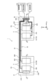
- FIG. 4 is a schematic top view showing an example of the configuration of the substrate shown in FIG.
- FIG. 5 is a schematic cross-sectional view showing an example of a laminated structure of the optical sensor taken along the line BB shown in FIG.
- FIG. 6 is a schematic cross-sectional view showing an example of a laminated structure of the optical sensor taken along the line CC shown in FIG.
- FIG. 1 is a schematic diagram showing an example of the external appearance of a detection device according to a first embodiment when a finger is placed inside the detection device as viewed from the side of a housing.
- FIG. 2 is a schematic cross-sectional
- the flexible printed circuit board 70 is formed in a deformable belt shape, and is formed into a ring shape by connecting one end 71 and the other end 72.
- the flexible printed circuit board 70 has a first mounting area 73 and a second mounting area 74.
- the first mounting area 73 is an area where the light source 60 and the like are mounted.
- the second mounting area 74 is an area where the control circuit 122, the power supply circuit 123, and the like are mounted.
- the flexible printed circuit board 70 has a board 21 mounted so as to straddle the vicinity of the light source 60 in the first mounting area 73.
- the board 21 is a sensor board on which the first optical sensor 10A, the second optical sensor 10B, and the like are mounted.
- the flexible printed circuit board 70 electrically connects the light source 60, the first optical sensor 10A, the second optical sensor 10B, and the like to the control circuit 122.
- the first optical sensor 10A and the second optical sensor 10B are arranged so as to sandwich the light source 60 in the circumferential direction 200C. That is, the detection device 1 is arranged in the circumferential direction 200C with the first optical sensor 10A, the light source 60, and the second optical sensor 10B in that order.
- the first optical sensor 10A and the second optical sensor 10B are arranged so as to sandwich the light source 60 in the circumferential direction 200C, so that the light emitted by the light source 60 can be detected over a wide range of the housing 200.
- the detection device 1 further includes a substrate 21 and a terminal portion 40.
- the substrate 21 is an insulating substrate, and is formed in a strip shape using, for example, a film-like resin.
- the substrate 21 is a deformable substrate on which the first optical sensor 10A and the second optical sensor 10B are mounted.
- the substrate 21 is attached to the flexible printed circuit board 70, so that the first optical sensor 10A and the second optical sensor 10B are positioned on both sides of the light source 60 in the circumferential direction 200C of the housing 200.
- the substrate 21 has a cutout portion 22 between both ends of the substrate 21 in the circumferential direction 200C of the housing 200, that is, in the longitudinal direction.
- the substrate 21 is mounted with the first optical sensor 10A on one end 21A side of the cutout portion 22, and the second optical sensor 10B on the other end 21B side.
- the terminal portion 40 is provided at one end 21A in the longitudinal direction of the substrate 21.
- the terminal section 40 supplies power from the power supply circuit 123 to the first optical sensor 10A and the second optical sensor 10B.
- the flexible printed circuit board 70 is housed inside the housing 200 so that the surface on which the first optical sensor 10A, the second optical sensor 10B, and the light source 60 are mounted faces the inner peripheral surface 200B of the housing 200. If the flexible printed circuit board 70 is translucent, the first optical sensor 10A, the second optical sensor 10B, and the light source 60 may be mounted on the back surface opposite the front surface. In this case, the light source 60 may be positioned so that it emits light toward the flexible printed circuit board 70 and the light that has passed through the flexible printed circuit board 70 is emitted toward the outside of the housing 200.
- the light source 60 is provided inside the first housing 210 of the housing 200, and is configured to be able to irradiate light toward the finger Fg wearing the housing 200.
- an inorganic LED Light Emitting Diode
- an organic EL Organic Light Emitting Diode
- the light source 60 irradiates light of a predetermined wavelength.
- the light source 60 has multiple light sources so as to be able to irradiate near-infrared light, red light, and green light.
- the light emitted from the light source 60 is reflected by the surface of the object to be detected, such as a finger Fg, and enters the first optical sensor 10A and the second optical sensor 10B.
- the light emitted from the light source 60 may be reflected inside the finger Fg or pass through the finger Fg and enter the first optical sensor 10A and the second optical sensor 10B.
- Information about a living body includes, for example, the pulse wave, pulse, and blood vessel image of the finger or palm.
- the detection device 1 may be configured as a fingerprint detection device that detects fingerprints, or a vein detection device that detects blood vessel patterns such as veins.
- the first optical sensor 10A and the second optical sensor 10B each detect light emitted by the light source 60 and reflected by the finger Fg, etc., and light that is directly incident.
- the first optical sensor 10A and the second optical sensor 10B are organic photodiodes (OPDs).
- OPDs organic photodiodes
- the first optical sensor 10A is provided on the housing 200 so as to be adjacent to one end 61 of the light source 60 in the circumferential direction 200C of the housing 200.
- the second optical sensor 10B is provided on the housing 200 so as to be adjacent to the other end 62 of the light source 60 in the circumferential direction 200C of the housing 200.
- the first optical sensor 10A and the second optical sensor 10B have a photodiode PD (see FIG. 4), which is an organic photodiode.
- PD photodiode
- Each of the first optical sensor 10A and the second optical sensor 10B has two lower electrodes 11 arranged along the circumferential direction 200C.
- the first optical sensor 10A and the second optical sensor 10B are mounted on a single substrate 21 and are electrically connected to the flexible printed circuit board 70 via the substrate 21.
- the substrate 21 has a cutout portion 22 between the first optical sensor 10A and the second optical sensor 10B in the circumferential direction 200C of the housing 200. The cutout portion 22 will be described later.
- the first direction Dx is a direction in a plane parallel to the substrate 21 and is the same direction as the circumferential direction 200C.
- the second direction Dy is a direction in a plane parallel to the substrate 21 and is a direction perpendicular to the first direction Dx.
- the second direction Dy may intersect with the first direction Dx without being perpendicular thereto.
- the third direction Dz is a direction perpendicular to the first direction Dx and the second direction Dy.
- the third direction Dz is the normal direction of the substrate 21.
- plane view refers to the positional relationship when viewed from a direction perpendicular to the substrate 21.
- the first optical sensor 10A is configured by stacking two lower electrodes 11 aligned in the first direction Dx so that one upper electrode 15A covers them.
- the second optical sensor 10B is configured by stacking two lower electrodes 11 aligned in the first direction Dx so that one upper electrode 15B covers them.
- the upper electrode 15 includes the upper electrode 15A of the first optical sensor 10A and the upper electrode 15B of the second optical sensor 10B. Each of the upper electrode 15A and the upper electrode 15B covers the two lower electrodes 11 in a plan view.
- the upper electrode 15A and the upper electrode 15B have a rectangular surface shape and are independent electrodes that are not electrically connected.
- the substrate 21 has a first power supply electrode 25A and a second power supply electrode 25B extending along the second direction Dy.
- the first power supply electrode 25A is provided between one end 21A of the substrate 21 in the first direction Dx and the first optical sensor 10A.
- the second power supply electrode 25B is provided between the other end 21B of the substrate 21 in the first direction Dx and the second optical sensor 10B.
- the first power supply electrode 25A is electrically connected to the terminal portion 40 of the substrate 21 via the first wiring 26A, and a power signal is supplied from the power supply circuit 123 (see FIG. 3) via the terminal portion 40.
- the second power supply electrode 25B is electrically connected to the terminal portion 40 of the substrate 21 via the second wiring 26B, and a power signal is supplied from the power supply circuit 123 via the terminal portion 40.
- the upper electrode 15A of the first optical sensor 10A is connected to the first power supply electrode 25A via the conductive material 24, and is electrically connected to the terminal portion 40 via the first wiring 26A connected to the first power supply electrode 25A.
- the upper electrode 15B of the second optical sensor 10B is connected to the second power supply electrode 25B via the conductive material 24, and is electrically connected to the terminal portion 40 via the second wiring 26B connected to the second power supply electrode 25B.
- the conductive material 24 is formed of a conductive material, covers the entire surface of the first power supply electrode 25A or the second power supply electrode 25B, and electrically connects the first power supply electrode 25A and the upper electrode 15A, and the second power supply electrode 25B and the upper electrode 15B.
- the upper electrode 15A may be directly connected to the first power supply electrode 25A and the second power supply electrode 25B without using the conductive material 24.
- Each of the lower electrodes 11 of the first optical sensor 10A and the second optical sensor 10B is connected to the terminal portion 40 via the third wiring 26C.
- the multiple third wirings 26C of the substrate 21 are connected to the detection circuit 48 of the control circuit 122 via the terminal portion 40 and the signal lines of the flexible printed circuit board 70.
- the detection circuit 48 is electrically connected to the lower electrodes 11 of the first optical sensor 10A and the second optical sensor 10B via the signal lines.
- the detection circuit 48 may be formed as a circuit separate from the control circuit 122.
- the first power supply electrode 25A and the second power supply electrode 25B receive a power signal from the power supply circuit 123 via the terminal portion 40, and supply the power signal to the upper electrode 15A and the upper electrode 15B.
- the first power supply electrode 25A and the second power supply electrode 25B are formed in a substantially rectangular shape extending in the second direction Dy in a plan view, and have the same area (size).
- the first optical sensor 10A has a substrate 21 and a photodiode PD.
- the first optical sensor 10A further has a third wiring 26C, an insulating layer 27, and a sealing film 90.
- the substrate 21 has a third wiring 26C provided on its upper surface.
- the third wiring 26C is a shield layer, and is formed, for example, of a metal wiring, and is formed of a material having better conductivity than the lower electrode 11 of the photodiode PD.
- the third wiring 26C is provided in a layer between the substrate 21 and the photodiode PD in the third direction Dz.
- the third wiring 26C is electrically connected to the terminal portion 40 in the substrate 21 (see FIG. 4).
- the third wiring 26C may be formed, for example, in the same layer as the lower electrode 11, or may be formed of metal.
- the insulating layer 27 is provided on the substrate 21, covering the third wiring 26C.
- the insulating layer 27 may be an inorganic insulating film or an organic insulating film.
- the photodiode PD is provided on the insulating layer 27 as a sensor element.
- the photodiode PD has a lower electrode 11, a lower buffer layer 12, an active layer 13, an upper buffer layer 14, and an upper electrode 15 (15A).
- the photodiode PD is stacked in the third direction Dz perpendicular to the substrate 21 in the following order: the lower electrode 11, the lower buffer layer 12 (hole transport layer), the active layer 13, the upper buffer layer 14 (electron transport layer), and the upper electrode 15.
- the lower electrode 11 is the anode electrode of the photodiode PD and is formed of a conductive material having light transmission, such as ITO (Indium Tin Oxide).
- ITO Indium Tin Oxide
- the characteristics (e.g., voltage-current characteristics and resistance value) of the active layer 13 change depending on the light irradiated thereto.
- An organic material is used as the material of the active layer 13.
- the active layer 13 is a bulk heterostructure in which a p-type organic semiconductor and an n-type fullerene derivative (PCBM), which is an n-type organic semiconductor, are mixed.
- PCBM n-type fullerene derivative
- low molecular weight organic materials such as C60 (fullerene), PCBM (phenyl C61-butyric acid methyl ester), CuPc (copper phthalocyanine), F16CuPc (fluorinated copper phthalocyanine), rubrene (5,6,11,12-tetraphenyltetracene), and PDI (perylene derivative) can be used as the active layer 13.
- C60 fulllerene
- PCBM phenyl C61-butyric acid methyl ester
- CuPc copper phthalocyanine
- F16CuPc fluorinated copper phthalocyanine
- rubrene 5,6,11,12-tetraphenyltetracene
- PDI perylene derivative
- the active layer 13 can be formed by a deposition type (dry process) using these low molecular weight organic materials.
- the active layer 13 may be, for example, a laminated film of CuPc and F16CuPc, or a laminated film of rubrene and C60.
- the active layer 13 can also be formed by a coating type (wet process).
- the active layer 13 is made of a material that combines the above-mentioned low molecular weight organic material and a polymer organic material.
- the polymer organic material for example, P3HT (poly(3-hexylthiophene)), F8BT (F8-alt-benzothiadiazole), etc. can be used.
- the active layer 13 can be a film in which P3HT and PCBM are mixed, or a film in which F8BT and PDI are mixed.
- the lower buffer layer 12 is a hole transport layer.
- the upper buffer layer 14 is an electron transport layer.
- the lower buffer layer 12 and the upper buffer layer 14 are provided to facilitate the holes and electrons generated in the active layer 13 to reach the lower electrode 11 or the upper electrode 15.
- the lower buffer layer 12 (hole transport layer) is directly on top of the lower electrode 11 and is also provided in the region between adjacent lower electrodes 11.
- the active layer 13 is directly on top of the lower buffer layer 12.
- the material of the hole transport layer is a metal oxide layer. Tungsten oxide (WO 3 ), molybdenum oxide, or the like is used as the metal oxide layer.
- the upper buffer layer 14 (electron transport layer) is in direct contact with the active layer 13, and the upper electrode 15 is in direct contact with the upper buffer layer 14.
- the material used for the electron transport layer is ethoxylated polyethyleneimine (PEIE).
- the materials and manufacturing methods of the lower buffer layer 12, active layer 13, and upper buffer layer 14 are merely examples, and other materials and manufacturing methods may be used.
- the lower buffer layer 12 and upper buffer layer 14 are not limited to single-layer films, and may be formed as laminated films including an electron blocking layer and a hole blocking layer.
- the upper electrode 15 is provided on the upper buffer layer 14.
- the upper electrode 15 is a cathode electrode of the photodiode PD, and is formed continuously over the entire first optical sensor 10A and the second optical sensor 10B. In other words, the upper electrode 15 is provided continuously over the multiple photodiodes PD.
- the upper electrode 15 faces the multiple lower electrodes 11, sandwiching the lower buffer layer 12, the active layer 13, and the upper buffer layer 14.
- the upper electrode 15 is formed of a conductive material having translucency, such as ITO or IZO. A part of the end of the upper surface 150 of the upper electrode 15 is electrically connected to the conductive material 24.
- the conductive material 24 is electrically connected to the first power supply electrode 25A, and supplies a power signal from the first power supply electrode 25A to the upper electrode 15.
- the photodiode PD is well sealed by providing a sealing film 90 on the upper electrode 15, the conductive material 24, etc.
- the upper electrode 15 may be a laminated film of multiple light-transmitting conductive materials.
- the sealing film 90 is provided on the upper electrode 15.
- the sealing film 90 is an inorganic film such as a silicon nitride film or an aluminum oxide film, or a resin film such as acrylic.
- the sealing film 90 is not limited to a single layer, and may be a laminated film of two or more layers combining the inorganic film and the resin film.
- the sealing film 90 seals the photodiode PD well and can prevent moisture from entering from the upper surface side.
- the first optical sensor 10A is configured to protect the terminal portion 40, the substrate 21, etc. by covering the sealing film 90 to a part of the terminal portion 40 with a resin 91.
- the photodiode PD of the second optical sensor 10B has a lower electrode 11, a lower buffer layer 12, an active layer 13, an upper buffer layer 14, and an upper electrode 15 (15B).
- the first optical sensor 10A and the second optical sensor 10B are organic photodiodes.
- the second optical sensor 10B a portion of the end of the upper surface 150 of the upper electrode 15 is electrically connected to the conductive material 24, and the conductive material 24 is electrically connected to the second power supply electrode 25B.
- a power supply signal is supplied from the second power supply electrode 25B to the upper electrode 15.
- the photodiode PD is well sealed by providing a sealing film 90 on the upper electrode 15, the conductive material 24, etc.
- the cutout portion 22 is formed over a distance in the first direction Dx that is longer than the length of the light source 60.
- the cutout portion 22 is formed over a distance in the second direction Dy that is longer than the length of the light source 60 and shorter than the length (width) of the substrate 21.
- the substrate 21 is integrally formed by connecting the regions of the first optical sensor 10A and the second optical sensor 10B at the connecting portion 23 of the cutout portion 22.
- the cutout portion 22 is formed in a shape in which the light source 60 can be arranged. In this embodiment, the cutout portion 22 is formed in a substantially rectangular shape in a plan view, but may be, for example, a semicircular, triangular, polygonal, or other shape.
- the connecting portion 23 is provided with the second wiring 26B and the third wiring 26C.
- the terminal unit 40 is electrically connected to the flexible printed circuit board 70 (see FIG. 5).
- the terminal unit 40 is a device for electrically connecting the area of the first optical sensor 10A and the second optical sensor 10B of the substrate 21 to the control circuit 122 and the power supply circuit 123 of the flexible printed circuit board 70.
- the terminal unit 40 is mounted on the substrate 21 and is electrically connected to the first wiring 26A, the second wiring 26B, the third wiring 26C, etc. of the substrate 21.
- the first wiring 26A, the second wiring 26B, and the third wiring 26C are metal wires of the same layer on the substrate 21.
- the terminal unit 40 supplies a power signal (power) from the power supply circuit 123 to the first optical sensor 10A via the first wiring 26A.
- the terminal unit 40 supplies a power signal (power) from the power supply circuit 123 to the second optical sensor 10B via the second wiring 26B.
- the terminal unit 40 has a plurality of terminals and is configured to be electrically connectable to a plurality of wirings.
- the control circuit 122 is a circuit that supplies control signals to the multiple photodiodes PD to control the detection operation.
- the multiple photodiodes PD each output an electrical signal corresponding to the light irradiated thereon as a detection signal Vdet to the detection circuit 48.
- the detection signals Vdet of the multiple photodiodes PD are output to the detection circuit 48 in a time-division sequential manner.
- the multiple signal lines SL are electrically connected to the detection circuit 48 in a time-division sequential manner. In this way, the detection device 1 detects information about the object to be detected based on the detection signals Vdet from the multiple photodiodes PD.
- the above describes an example configuration of the detection device 1 according to this embodiment. Note that the above configuration described using Figures 1 to 6 is merely an example, and the configuration of the detection device 1 according to this embodiment is not limited to this example. The configuration of the detection device 1 according to this embodiment can be flexibly modified according to the specifications and operation.
- the detection device 1 can supply power from the first power supply electrode 25A and the second power supply electrode 25B to the upper electrodes 15A and 15B.
- the detection device 1 can reduce the resistance of the path between the upper electrodes 15A and 15B and the terminal portion 40 more than when a single common upper electrode is used, thereby reducing the difference in power supply capacity and preventing a difference in sensitivity between the first optical sensor 10A and the second optical sensor 10B.
- the detection device 1 uses multiple power supply electrodes, even if a malfunction occurs in one of the multiple optical sensors, the detection device 1 can reduce the possibility that both the first optical sensor 10A and the second optical sensor 10B will become unusable. As a result, the detection device 1 can detect information about the biological body of the finger Fg over the long term, even if the housing 200 is small and difficult to repair.
- the first wiring 26A and the second wiring 26B are metal wires in the same layer of the substrate 21 as the third wiring 26C connected to the lower electrode 11. This allows the detection device 1 to arrange the first power supply electrode 25A and the second power supply electrode 25B on the substrate 21 without complicating the configuration of the substrate 21.
- the detection device 1 provides a first power supply electrode 25A between one end 21A of the substrate 21 in the first direction Dx and the first optical sensor 10A, and provides a second power supply electrode 25B between the other end 21B of the substrate 21 in the first direction Dx and the second optical sensor 10B. This allows the detection device 1 to provide the first optical sensor 10A and the second optical sensor 10B of the substrate 21 near the cutout portion 22, so that the first optical sensor 10A and the second optical sensor 10B can be brought close to each other across the cutout portion 22.
- the detection device 1 includes a light source 60 that is disposed in the cutout portion 22 of the substrate 21. This allows the detection device 1 to dispose the first optical sensor 10A and the second optical sensor 10B near the cutout portion 22 of the substrate 21, and by bringing them closer to the light source 60, the sensitivity of the first optical sensor 10A and the second optical sensor 10B can be improved.
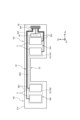
- FIG. 7 is a schematic top view showing a configuration example of a reference example substrate according to embodiment 1.
- the upper electrode 15A and the upper electrode 15B are integrally formed by the electrode connection portion 15C of the connection portion 23.
- the lower buffer layer 12, the active layer 13, the upper buffer layer 14, and the electrode connection portion 151 of the upper electrode 15 are arranged in the connection portion 23.
- the electrode connection portion 15C and the upper electrodes 15 of the first optical sensor 10A and the second optical sensor 10B are integrally formed.
- the reference example substrate 21X supplies power to the first optical sensor 10A and the second optical sensor 10B from one first power supply electrode 25A.
- the detection device 1 according to the first embodiment is configured to supply power from the first power supply electrode 25A to the upper electrode 15A of the first optical sensor 10A, and from the second power supply electrode 25B to the upper electrode 15B of the second optical sensor 10B.
- This allows the detection device 1 to suppress an increase in the resistance value from the terminal portion 40 to the upper electrode 15A and the upper electrode 15B, thereby reducing the sensitivity difference between the first optical sensor 10A and the second optical sensor 10B.
- the detection device 1 according to the first embodiment uses multiple power supply electrodes, even if a malfunction occurs in the sensor element of the first optical sensor 10A or the second optical sensor 10B, it is possible to reduce the possibility that all of the optical sensors will become unusable.
- (Embodiment 2) 8 is a top view schematic diagram showing a configuration example of the substrate 21 of the detection device 1 according to the second embodiment.
- the detection device 1 includes the substrate 21, the terminal portion 40, the first optical sensor 10A, and the second optical sensor 10B described above.
- the substrate 21 has a first power supply electrode 25A and a second power supply electrode 25C extending along the second direction Dy.
- the second power supply electrode 25C is formed so that the length in the first direction Dx is the same as that of the second power supply electrode 25B described above, and is longer than the first power supply electrode 25A in the second direction Dy intersecting with the first direction Dx, and has a larger electrode area.
- the second power supply electrode 25C is electrically connected to the terminal portion 40 of the substrate 21 via the second wiring 26B, and a power signal is supplied from the power supply circuit 123 via the terminal portion 40.
- the upper electrode 15B of the second optical sensor 10B is connected to the second power supply electrode 25C, and is also electrically connected to the terminal portion 40 via the second wiring 26B connected to the second power supply electrode 25B. That is, the upper electrode 15B of the second optical sensor 10B has a larger contact area with the second power supply electrode 25B than when the first power supply electrode 25A is used.
- the upper electrode 15A and the upper electrode 15B are each supplied with power from independent systems of the first power supply electrode 25A and the second power supply electrode 25B.
- the detection device 1 can prevent the resistance value of the path from the terminal portion 40 to the upper electrode 15B from increasing by reducing the resistance value of the second power supply electrode 25C. This allows the detection device 1 to reduce the difference in resistance between the path from the terminal portion 40 to the upper electrode 15A and the path from the terminal portion 40 to the upper electrode 15B. As a result, the detection device 1 can reduce the difference in sensor sensitivity between the first optical sensor 10A closer to the terminal portion 40 and the second optical sensor 10B farther away from the terminal portion 40 than the first optical sensor 10A, and can accommodate larger substrates 21.
- the second power supply electrode 25C is formed so that the length in the second direction Dy is longer than that of the first power supply electrode 25A, but the length in the first direction Dx may be longer.
- the second power supply electrode 25C may have the same length and surface area as the first power supply electrode 25A, but may have a different thickness.
- the substrate 21-1 has three first power supply electrodes 25A extending along the second direction Dy.
- Each of the three first power supply electrodes 25A is electrically connected to the terminal portion 40 of the substrate 21-1 via the first wiring 26A, and a power signal is supplied from the power supply circuit 123 (see FIG. 3) via the terminal portion 40.
- Each of the upper electrodes 15A of the three first optical sensors 10A is connected to the first power supply electrode 25A via the conductive material 24, and is electrically connected to the terminal portion 40 via the first wiring 26A connected to the first power supply electrode 25A. As a result, the three upper electrodes 15A are supplied with power from independent power systems to the respective first power supply electrodes 25A.
- each of the three first optical sensors 10A has a substrate 21-1, a photodiode PD, a third wiring 26C, and an insulating layer 27.
- the photodiode PD of the first optical sensor 10A has a lower electrode 11, a lower buffer layer 12, an active layer 13, an upper buffer layer 14, and an upper electrode 15 (15A).
- the three first power supply electrodes 25A are electrically connected to the terminal portion 40 of the substrate 21-1 via the first wiring 26A, and a power signal is supplied from the power supply circuit 123 via the terminal portion 40.
- Each of the upper electrodes 15B of the three first optical sensors 10A is connected to the corresponding first power supply electrode 25A, and is electrically connected to the terminal portion 40 via the first wiring 26A connected to the first power supply electrode 25A.
- each of the three upper electrodes 15A is supplied with power from an independent system for each first power supply electrode 25A.
- Each of the lower electrodes 11 of the three first optical sensors 10 is electrically connected to the terminal portion 40 via the third wiring 26C of the substrate 21-1.
- the detection device 1 supplies a power signal from the power supply circuit 123 to each of the three upper electrodes 15A via the three first power supply electrodes 25A.
- the detection device 1 turns on the light source 60, causing the light source 60 to irradiate light toward the finger Fg.
- the light source 60 irradiates light to one side and the other side in the circumferential direction 200C.
- the detection device 1 receives light reflected by the finger Fg or the like with the three first optical sensors 10A.
- the detection device 1 detects information about the living body of the finger Fg based on the amount of light received detected by each of the two photodiodes PD of the three first optical sensors 10A.
- the detection device 1 can supply power from the three first power supply electrodes 25A to each of the upper electrodes 15A of the three first optical sensors 10A to operate each lower electrode 11.
- the detection device 1 arranges the three first optical sensors 10A side by side in the circumferential direction 200C of the housing 200, it is possible to suppress differences in the power supply capabilities of the three upper electrodes 15A and prevent differences in sensitivity among the three first optical sensors 10A.
- FIG. 11 is a top schematic diagram showing a configuration example of a reference example substrate according to embodiment 3.
- six lower electrodes 11 are arranged in a line along the first direction Dx, and an upper electrode 15Y is arranged to cover all of the six lower electrodes 11, thereby forming one optical sensor 10Y.
- the reference example substrate 21Y supplies power to the optical sensor 10Y from one first power supply electrode 25A.
- the detection device 1 according to embodiment 3 is configured to supply power from three first power supply electrodes 25A to the upper electrodes 15A of the three first optical sensors 10A. This allows the detection device 1 to prevent the resistance value of the path to the three upper electrodes 15A from increasing, thereby reducing the sensitivity difference between the three first optical sensors 10A. Furthermore, the detection device 1 according to embodiment 3 can prevent all of the first optical sensors 10A from becoming unusable even if a malfunction occurs in an element of one of the three first optical sensors 10A.
- (Embodiment 4) 12 is a top schematic diagram showing a configuration example of the substrate 21-1 of the detection device 1 according to the fourth embodiment.
- the detection device 1 includes the above-mentioned substrate 21-1, the terminal portion 40, and three first optical sensors 10A.
- the substrate 21-1 includes the first power supply electrode 25A1, the first power supply electrode 25A2, and the first power supply electrode 25A3 extending along the second direction Dy.
- the first power supply electrode 25A1, the first power supply electrode 25A2, and the first power supply electrode 25A3 are formed so that the length of the substrate 21-1 in the second direction Dy increases with increasing distance from the terminal portion 40.
- the first power supply electrode 25A1, the first power supply electrode 25A2, and the first power supply electrode 25A3 have the same length in the first direction Dx. That is, the electrode area of the first power supply electrode 25A1, the first power supply electrode 25A2, and the first power supply electrode 25A3 increases with increasing distance from the terminal portion 40.
- Each of the first power supply electrodes 25A1, 25A2, and 25A3 is electrically connected to a terminal portion 40 of the substrate 21 via the third wiring 26C, and a power signal is supplied from the power supply circuit 123 via the terminal portion 40.
- Each of the first power supply electrodes 25A1, 25A2, and 25A3 is electrically connected to the corresponding upper electrode 15A of the first optical sensor 10A via the conductive material 24, and is also electrically connected to the terminal portion 40 via the second wiring 26B.
- each of the upper electrodes 15A of the three first optical sensors 10A is supplied with power from the independent systems of the first power supply electrodes 25A2 and 25A3.
- the detection device 1 is described as containing the substrate 21, substrate 21-1, etc. inside the ring-shaped housing 200, but this is not limited to the above.
- the detection device 1 may be, for example, contained in a rectangular housing, or may be attached to the object to be measured without being contained in a housing.
- the detection device 1 has been described as being connected to the first power supply electrode 25A, the second power supply electrode 25B, the second power supply electrode 25C, etc. by wiring, but is not limited to this.
- the detection device 1 may use the first power supply electrode 25A, the second power supply electrode 25B, the second power supply electrode 25C, etc. as the tip of the wiring.
Landscapes
- Engineering & Computer Science (AREA)
- Health & Medical Sciences (AREA)
- Life Sciences & Earth Sciences (AREA)
- Physics & Mathematics (AREA)
- Molecular Biology (AREA)
- General Health & Medical Sciences (AREA)
- Biophysics (AREA)
- Biomedical Technology (AREA)
- Heart & Thoracic Surgery (AREA)
- Medical Informatics (AREA)
- Theoretical Computer Science (AREA)
- Surgery (AREA)
- Animal Behavior & Ethology (AREA)
- Pathology (AREA)
- Public Health (AREA)
- Veterinary Medicine (AREA)
- Human Computer Interaction (AREA)
- General Physics & Mathematics (AREA)
- Multimedia (AREA)
- Electromagnetism (AREA)
- Light Receiving Elements (AREA)
- Image Input (AREA)
Priority Applications (2)
| Application Number | Priority Date | Filing Date | Title |
|---|---|---|---|
| JP2025513873A JPWO2024214533A1 (https=) | 2023-04-14 | 2024-03-26 | |
| US19/354,576 US20260038299A1 (en) | 2023-04-14 | 2025-10-09 | Detection device |
Applications Claiming Priority (2)
| Application Number | Priority Date | Filing Date | Title |
|---|---|---|---|
| JP2023-066376 | 2023-04-14 | ||
| JP2023066376 | 2023-04-14 |
Related Child Applications (1)
| Application Number | Title | Priority Date | Filing Date |
|---|---|---|---|
| US19/354,576 Continuation US20260038299A1 (en) | 2023-04-14 | 2025-10-09 | Detection device |
Publications (1)
| Publication Number | Publication Date |
|---|---|
| WO2024214533A1 true WO2024214533A1 (ja) | 2024-10-17 |
Family
ID=93059112
Family Applications (1)
| Application Number | Title | Priority Date | Filing Date |
|---|---|---|---|
| PCT/JP2024/012031 Ceased WO2024214533A1 (ja) | 2023-04-14 | 2024-03-26 | 検出装置 |
Country Status (3)
| Country | Link |
|---|---|
| US (1) | US20260038299A1 (https=) |
| JP (1) | JPWO2024214533A1 (https=) |
| WO (1) | WO2024214533A1 (https=) |
Citations (3)
| Publication number | Priority date | Publication date | Assignee | Title |
|---|---|---|---|---|
| JPS61166162A (ja) * | 1985-01-18 | 1986-07-26 | Ricoh Co Ltd | イメ−ジセンサ |
| JP2015229068A (ja) * | 2014-06-06 | 2015-12-21 | ローム株式会社 | センサプローブ |
| JP2018044984A (ja) * | 2016-09-12 | 2018-03-22 | 株式会社ジャパンディスプレイ | 表示装置 |
-
2024
- 2024-03-26 JP JP2025513873A patent/JPWO2024214533A1/ja active Pending
- 2024-03-26 WO PCT/JP2024/012031 patent/WO2024214533A1/ja not_active Ceased
-
2025
- 2025-10-09 US US19/354,576 patent/US20260038299A1/en active Pending
Patent Citations (3)
| Publication number | Priority date | Publication date | Assignee | Title |
|---|---|---|---|---|
| JPS61166162A (ja) * | 1985-01-18 | 1986-07-26 | Ricoh Co Ltd | イメ−ジセンサ |
| JP2015229068A (ja) * | 2014-06-06 | 2015-12-21 | ローム株式会社 | センサプローブ |
| JP2018044984A (ja) * | 2016-09-12 | 2018-03-22 | 株式会社ジャパンディスプレイ | 表示装置 |
Also Published As
| Publication number | Publication date |
|---|---|
| US20260038299A1 (en) | 2026-02-05 |
| JPWO2024214533A1 (https=) | 2024-10-17 |
Similar Documents
| Publication | Publication Date | Title |
|---|---|---|
| WO2023199793A1 (ja) | 検出装置 | |
| US10644186B2 (en) | Bio-information detecting sensor | |
| US12541226B2 (en) | Detection device | |
| US12560964B2 (en) | Detection device | |
| US12560967B2 (en) | Annular housing for detection device with first and second flexible substrates | |
| WO2024034431A1 (ja) | 検出装置 | |
| US20260040754A1 (en) | Detection device | |
| US20260032825A1 (en) | Detection device | |
| WO2024214533A1 (ja) | 検出装置 | |
| US20260038301A1 (en) | Detection device | |
| US20260083399A1 (en) | Sensor and detection device | |
| WO2026034320A1 (ja) | 検出装置 | |
| US20260076085A1 (en) | Sensor and detection device | |
| WO2025110058A1 (ja) | 検出装置 | |
| WO2026034352A1 (ja) | 検出装置 | |
| JP7823184B2 (ja) | 検出装置 | |
| WO2023223877A1 (ja) | 検出装置 | |
| WO2025110083A1 (ja) | 検出装置 | |
| WO2025037531A1 (ja) | 検出装置 | |
| US20250015120A1 (en) | Detection device | |
| WO2025253946A1 (ja) | 検出装置の製造方法 | |
| WO2026009704A1 (ja) | 検出装置及び検出装置の製造方法 | |
| US20260033723A1 (en) | Detection device | |
| US20240423003A1 (en) | Detection device | |
| WO2026009689A1 (ja) | 検出装置及び検出装置の製造方法 |
Legal Events
| Date | Code | Title | Description |
|---|---|---|---|
| 121 | Ep: the epo has been informed by wipo that ep was designated in this application |
Ref document number: 24788561 Country of ref document: EP Kind code of ref document: A1 |
|
| ENP | Entry into the national phase |
Ref document number: 2025513873 Country of ref document: JP Kind code of ref document: A |
|
| WWE | Wipo information: entry into national phase |
Ref document number: 2025513873 Country of ref document: JP |
|
| NENP | Non-entry into the national phase |
Ref country code: DE |
|
| 122 | Ep: pct application non-entry in european phase |
Ref document number: 24788561 Country of ref document: EP Kind code of ref document: A1 |