WO2024210129A1 - 合成単結晶ダイヤモンド、合成単結晶ダイヤモンドの製造方法および赤外光学部品 - Google Patents
合成単結晶ダイヤモンド、合成単結晶ダイヤモンドの製造方法および赤外光学部品 Download PDFInfo
- Publication number
- WO2024210129A1 WO2024210129A1 PCT/JP2024/013623 JP2024013623W WO2024210129A1 WO 2024210129 A1 WO2024210129 A1 WO 2024210129A1 JP 2024013623 W JP2024013623 W JP 2024013623W WO 2024210129 A1 WO2024210129 A1 WO 2024210129A1
- Authority
- WO
- WIPO (PCT)
- Prior art keywords
- single crystal
- diamond
- synthetic single
- crystal diamond
- less
- Prior art date
- Legal status (The legal status is an assumption and is not a legal conclusion. Google has not performed a legal analysis and makes no representation as to the accuracy of the status listed.)
- Ceased
Links
Images


Classifications
-
- C—CHEMISTRY; METALLURGY
- C30—CRYSTAL GROWTH
- C30B—SINGLE-CRYSTAL GROWTH; UNIDIRECTIONAL SOLIDIFICATION OF EUTECTIC MATERIAL OR UNIDIRECTIONAL DEMIXING OF EUTECTOID MATERIAL; REFINING BY ZONE-MELTING OF MATERIAL; PRODUCTION OF A HOMOGENEOUS POLYCRYSTALLINE MATERIAL WITH DEFINED STRUCTURE; SINGLE CRYSTALS OR HOMOGENEOUS POLYCRYSTALLINE MATERIAL WITH DEFINED STRUCTURE; AFTER-TREATMENT OF SINGLE CRYSTALS OR A HOMOGENEOUS POLYCRYSTALLINE MATERIAL WITH DEFINED STRUCTURE; APPARATUS THEREFOR
- C30B29/00—Single crystals or homogeneous polycrystalline material with defined structure characterised by the material or by their shape
- C30B29/02—Elements
- C30B29/04—Diamond
-
- B—PERFORMING OPERATIONS; TRANSPORTING
- B01—PHYSICAL OR CHEMICAL PROCESSES OR APPARATUS IN GENERAL
- B01J—CHEMICAL OR PHYSICAL PROCESSES, e.g. CATALYSIS OR COLLOID CHEMISTRY; THEIR RELEVANT APPARATUS
- B01J3/00—Processes of utilising sub-atmospheric or super-atmospheric pressure to effect chemical or physical change of matter; Apparatus therefor
- B01J3/06—Processes using ultra-high pressure, e.g. for the formation of diamonds; Apparatus therefor, e.g. moulds or dies
- B01J3/065—Presses for the formation of diamonds or boronitrides
-
- C—CHEMISTRY; METALLURGY
- C30—CRYSTAL GROWTH
- C30B—SINGLE-CRYSTAL GROWTH; UNIDIRECTIONAL SOLIDIFICATION OF EUTECTIC MATERIAL OR UNIDIRECTIONAL DEMIXING OF EUTECTOID MATERIAL; REFINING BY ZONE-MELTING OF MATERIAL; PRODUCTION OF A HOMOGENEOUS POLYCRYSTALLINE MATERIAL WITH DEFINED STRUCTURE; SINGLE CRYSTALS OR HOMOGENEOUS POLYCRYSTALLINE MATERIAL WITH DEFINED STRUCTURE; AFTER-TREATMENT OF SINGLE CRYSTALS OR A HOMOGENEOUS POLYCRYSTALLINE MATERIAL WITH DEFINED STRUCTURE; APPARATUS THEREFOR
- C30B33/00—After-treatment of single crystals or homogeneous polycrystalline material with defined structure
- C30B33/04—After-treatment of single crystals or homogeneous polycrystalline material with defined structure using electric or magnetic fields or particle radiation
-
- C—CHEMISTRY; METALLURGY
- C30—CRYSTAL GROWTH
- C30B—SINGLE-CRYSTAL GROWTH; UNIDIRECTIONAL SOLIDIFICATION OF EUTECTIC MATERIAL OR UNIDIRECTIONAL DEMIXING OF EUTECTOID MATERIAL; REFINING BY ZONE-MELTING OF MATERIAL; PRODUCTION OF A HOMOGENEOUS POLYCRYSTALLINE MATERIAL WITH DEFINED STRUCTURE; SINGLE CRYSTALS OR HOMOGENEOUS POLYCRYSTALLINE MATERIAL WITH DEFINED STRUCTURE; AFTER-TREATMENT OF SINGLE CRYSTALS OR A HOMOGENEOUS POLYCRYSTALLINE MATERIAL WITH DEFINED STRUCTURE; APPARATUS THEREFOR
- C30B9/00—Single-crystal growth from melt solutions using molten solvents
- C30B9/04—Single-crystal growth from melt solutions using molten solvents by cooling of the solution
- C30B9/08—Single-crystal growth from melt solutions using molten solvents by cooling of the solution using other solvents
- C30B9/10—Metal solvents
-
- G—PHYSICS
- G02—OPTICS
- G02B—OPTICAL ELEMENTS, SYSTEMS OR APPARATUS
- G02B1/00—Optical elements characterised by the material of which they are made; Optical coatings for optical elements
- G02B1/02—Optical elements characterised by the material of which they are made; Optical coatings for optical elements made of crystals, e.g. rock-salt, semi-conductors
-
- G—PHYSICS
- G02—OPTICS
- G02B—OPTICAL ELEMENTS, SYSTEMS OR APPARATUS
- G02B5/00—Optical elements other than lenses
- G02B5/20—Filters
- G02B5/22—Absorbing filters
-
- C—CHEMISTRY; METALLURGY
- C01—INORGANIC CHEMISTRY
- C01B—NON-METALLIC ELEMENTS; COMPOUNDS THEREOF; METALLOIDS OR COMPOUNDS THEREOF NOT COVERED BY SUBCLASS C01C
- C01B32/00—Carbon; Compounds thereof
- C01B32/25—Diamond
- C01B32/28—After-treatment, e.g. purification, irradiation, separation or recovery
Definitions
- This disclosure relates to synthetic single crystal diamond, a method for producing synthetic single crystal diamond, and infrared optical components.
- This application claims priority to Japanese Patent Application No. 2023-060358, filed on April 3, 2023. All contents of said Japanese Patent Application are incorporated herein by reference.
- Synthetic diamond which has excellent properties such as a wide transmission range and scratch resistance, is being considered as a material for optical components used in infrared spectroscopic analysis.
- Patent document 1 JP Patent Publication 6-214102 discusses an infrared optical component consisting of a total reflection prism made of synthetic diamond with a nitrogen content of 3 ppm or less and a boron content of 3 ppm or less.
- the synthetic single crystal diamond of the present disclosure is A synthetic single crystal diamond having a nitrogen content of 1 ppm or less based on the atomic number of atoms and a boron content of 0.01 ppm or more and 3 ppm or less based on the atomic number of atoms, the content of boron based on atomic number is greater than the content of nitrogen based on atomic number,
- the synthetic single crystal diamond has no absorption peak in the wave number range of 2790 cm -1 or more and 2810 cm -1 or less in an infrared absorption spectrum measured by Fourier transform infrared spectroscopy.
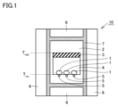
- FIG. 1 is a schematic cross-sectional view showing an example of a sample chamber configuration for use in producing synthetic single crystal diamond according to one embodiment of the present disclosure.
- FIG. 2 is a diagram showing an infrared absorption spectrum of the diamond single crystal produced in Sample 7 before electron beam irradiation.
- FIG. 3 is a diagram showing an infrared absorption spectrum of the synthetic single crystal diamond produced from sample 7 after electron beam irradiation.
- the boron in synthetic diamond is an inevitable impurity contained in the carbon source (diamond powder or graphite powder) used in the synthesis, and is incorporated into the crystal during synthesis.
- the infrared absorption spectrum of the synthetic diamond shows absorption in the wave number range of 2790 cm -1 to 2810 cm -1 , which becomes background noise.
- the synthetic single crystal diamond cannot be used as an optical component for evaluating optical properties with an infrared optical analyzer.
- the present disclosure therefore aims to provide a synthetic single crystal diamond that can be used as an infrared optical component.
- the synthetic single crystal diamond of the present disclosure is A synthetic single crystal diamond having a nitrogen content of 1 ppm or less based on the atomic number of atoms and a boron content of 0.01 ppm or more and 3 ppm or less based on the atomic number of atoms, the content of boron based on atomic number is greater than the content of nitrogen based on atomic number,
- the synthetic single crystal diamond has no absorption peak in the wave number range of 2790 cm -1 or more and 2810 cm -1 or less in an infrared absorption spectrum measured by Fourier transform infrared spectroscopy.
- This disclosure makes it possible to provide synthetic single crystal diamond that can be used as an infrared optical component.
- the Knoop hardness in the ⁇ 100> direction on the ⁇ 001 ⁇ face of the synthetic single crystal diamond may be 80 GPa or more.
- the Knoop hardness is measured in accordance with JIS Z 2251:2009 at a temperature of 23°C ⁇ 5°C and a test load of 4.9 N.
- synthetic single crystal diamond can be ideally used as a material for infrared optical components such as compression cells, which require particularly high hardness, ATR prisms, sample plates, high-pressure resistant windows, and anvils for generating high pressure.
- the crack initiation load of the synthetic single crystal diamond may be 10 N or more.
- the crack initiation load is measured in a fracture strength test in which a spherical diamond indenter with a tip radius of 50 ⁇ m is pressed against the surface of the synthetic single crystal diamond at a load rate of 100 N/min.
- synthetic single crystal diamond can be ideally used as a material for infrared optical components such as compression cells, which require particularly high strength, ATR prisms, sample plates, high-pressure resistant windows, and anvils for generating high pressure.
- This disclosure makes it possible to provide synthetic single crystal diamond that can be used as an infrared optical component.
- the diamond single crystal may be irradiated with the electron beam under conditions of an energy of 1.0 MeV to 10 MeV and a dose of 1.0 x 10 e/ m2 to 1.0 x 10 e/ m2 , thereby providing the diamond single crystal with energy of 1 MGy to less than 10 MGy.
- the infrared optical component of the present disclosure is an infrared optical component that includes a synthetic single crystal diamond described in any one of (1) to (3) above.
- This disclosure makes it possible to provide infrared optical components that do not exhibit background noise when measuring infrared optical spectra.
- a ⁇ B means the upper and lower limits of a range (i.e., greater than or equal to A and less than or equal to B). If no unit is stated for A and only a unit is stated for B, the units of A and B are the same.
- any one numerical value listed as the lower limit and any one numerical value listed as the upper limit is also considered to be disclosed.
- a1 or more, b1 or more, and c1 or more are listed as the lower limit and a2 or less, b2 or less, and c2 or less are listed as the upper limit, a1 or more and a2 or less, a1 or more and b2 or less, a1 or more and c2 or less, b1 or more and a2 or less, b1 or more and b2 or less, b1 or more and c2 or less, c1 or more and a2 or less, c1 or more and b2 or less, and c1 or more and c2 or less are considered to be disclosed.
- a synthetic single crystal diamond according to one embodiment of the present disclosure (hereinafter also referred to as “embodiment 1”) is A synthetic single crystal diamond having a nitrogen content based on the number of atoms (hereinafter also referred to as “nitrogen content”) of 1 ppm or less and a boron content based on the number of atoms (hereinafter also referred to as "boron content”) of 0.01 ppm or more and 3 ppm or less, The content of boron based on atomic number is greater than the content of nitrogen based on atomic number, This synthetic single crystal diamond has no absorption peak in the wavenumber range of 2790 cm -1 or more and 2810 cm -1 or less in an infrared absorption spectrum measured by Fourier transform infrared spectroscopy.
- the nitrogen content of the synthetic single crystal diamond of embodiment 1 is 1 ppm or less and less than the boron content.
- the upper limit of the nitrogen content of the synthetic single crystal diamond is less than the boron content and 1 ppm or less from the viewpoint of suppressing background noise during infrared optical spectrum measurement, and may be 0.8 ppm or less, 0.05 ppm or less, 0.04 ppm or less, 0.03 ppm or less, or 0.02 ppm or less.
- the lower limit of the nitrogen content of the synthetic single crystal diamond is not particularly limited, and may be 0 ppm or more, or 0.008 ppm or more.
- the nitrogen content of the synthetic single crystal diamond may be 0 ppm or more and 1 ppm or less, 0.008 ppm or more and 1 ppm or less, 0 ppm or more and 0.8 ppm or less, or 0.008 ppm or more and 0.8 ppm or less.
- the nitrogen content of the synthetic single crystal diamond is measured by secondary ion mass spectrometry (SIMS) using a CAMECA "IMS-7f" (trademark) measuring device and 15.0 keV Cs + ions as the primary ion beam.
- SIMS secondary ion mass spectrometry
- the boron content of the synthetic single crystal diamond of embodiment 1 is 0.01 ppm or more and 3 ppm or less, and is greater than the nitrogen content.
- the upper limit of the boron content of synthetic single crystal diamond is 3 ppm or less, may be 2.3 ppm or less, may be 1.5 ppm or less, may be 0.21 ppm or less, may be 0.19 ppm or less, or may be 0.11 ppm or less, from the viewpoint of suppressing background noise during infrared optical spectrum measurement.
- the lower limit of the boron content of synthetic single crystal diamond is 0.01 ppm or more, may be 0.05 ppm or more.
- the boron content of synthetic single crystal diamond is 0.01 ppm or more and 3 ppm or less, may be 0.01 ppm or more and 2.3 ppm or less, or may be 0.05 ppm or more and 2.3 ppm or less.
- the boron content of synthetic single crystal diamond is measured by secondary ion mass spectrometry (SIMS).
- SIMS secondary ion mass spectrometry
- the synthetic single crystal diamond of embodiment 1 may contain impurities other than nitrogen and boron. These impurities include, for example, hydrogen.
- the total content of the impurities other than nitrogen and boron in the synthetic single crystal diamond of embodiment 1 based on atomic number can be 10ppm or less.
- the absence of an absorption peak in the wave number range of 2790 cm -1 to 2810 cm -1 in the infrared absorption spectrum means that no absorption other than the inherent absorption spectrum of diamond is observed in the spectrum in the wave number range. This means that no maximum value is present in the infrared absorption spectrum in the wave number range of 2790 cm -1 to 2810 cm -1 in the macroscopic view.
- the inherent absorption spectrum of diamond in the wave number range of 2790 cm -1 to 2810 cm -1 corresponds to the infrared absorption spectrum shown in FIG. 3, for example.
- the horizontal axis indicates the wave number (cm -1 )
- the vertical axis indicates the intensity.
- the infrared absorption spectrum of synthetic single crystal diamond is obtained by measurement using Fourier transform infrared spectroscopy at a temperature of 23°C ⁇ 2°C (21°C or higher and 25°C or lower).
- the measurement procedure is as follows.
- the synthetic single crystal diamond sample to be measured is processed into a plate with a thickness of approximately 1 mm, and the two light-transmitting surfaces are polished with a metal-bonded grinding wheel so that the surface roughness Ra is 20 nm or less.
- the polished surfaces are irradiated with infrared light to create an infrared absorption spectrum.
- the temperature change of the measuring equipment and sample during measurement is kept to within ⁇ 1°C.
- the present inventors have found a method for obtaining a synthetic single crystal diamond that does not have an absorption peak in the wave number range of 2790 cm ⁇ 1 to 2810 cm ⁇ 1 in the infrared absorption spectrum, even when the boron content is more than the nitrogen content, and have completed the synthetic single crystal diamond of the present disclosure.
- the Knoop hardness in the ⁇ 100> direction on the ⁇ 001 ⁇ plane of the synthetic single crystal diamond of embodiment 1 may be 80 GPa or more.
- the synthetic single crystal diamond can be suitably used as a material for components such as compression cells, ATR prisms, sample plates, high-pressure windows or high-pressure generating anvils, which require particularly high hardness.
- the lower limit of the ⁇ 001 ⁇ 100> Knoop hardness of synthetic single crystal diamond may be 80 GPa or more, 83 GPa or more, 87 GPa or more, or 90 GPa or more.
- the upper limit of the ⁇ 001 ⁇ 100> Knoop hardness is not particularly limited, but may be, for example, 100 GPa or less, 96 GPa or less, or 94 GPa or less.
- the ⁇ 001 ⁇ 100> Knoop hardness may be 80 GPa or more and 100 GPa or less, 80 GPa or more and 96 GPa or less, or 83 GPa or more and 96 GPa or less.
- the ⁇ 001 ⁇ 100> Knoop hardness (units: GPa) of synthetic single crystal diamond is measured in accordance with JIS Z 2251:2009 at a temperature of 23°C ⁇ 5°C (18°C to 28°C) and a test load of 4.9N.
- the measurement procedure is as follows. First, an indentation is made in the ⁇ 100> direction in the ⁇ 001 ⁇ plane of the synthetic single crystal diamond with a load of 4.9N. The diagonal a ( ⁇ m) on the longer side of the indentation is measured, and the ⁇ 001 ⁇ 100> Knoop hardness is calculated using the following formula.
- the crack initiation load of the synthetic single crystal diamond of embodiment 1 is preferably 10N or more.
- synthetic single crystal diamond has excellent fracture strength and chipping resistance.
- this synthetic single crystal diamond can be suitably used as the material of infrared optical components such as compression cell, ATR prism, sample plate, high pressure window or high pressure generation anvil, which require high strength.
- the lower limit of the crack initiation load for synthetic single crystal diamond may be 10N or more, 12N or more, 15N or more, or 16N or more.
- the upper limit of the crack initiation load is not particularly limited, but from a manufacturing standpoint, it can be 50N or less, or may be 16N or less.
- the crack initiation load for synthetic single crystal diamond may be 10N or more and 50N or less, 12N or more and 50N or less, or 15N or more and 50N or less.
- the crack initiation load of synthetic single crystal diamond is measured using the following procedure.
- a spherical diamond indenter with a tip radius (R) of 50 ⁇ m is pressed against the (100) face of the synthetic single crystal diamond.
- a load is applied to the single crystal diamond at a loading rate of 100 N/min, and the load (crack initiation load) is measured at the moment a crack occurs in the synthetic single crystal diamond.
- the moment a crack occurs is measured with an AE sensor.
- the measurement temperature is 25°C.
- a method for producing a synthetic single crystal diamond according to one embodiment of the present disclosure (hereinafter also referred to as "embodiment 2") is the method for producing a synthetic single crystal diamond according to embodiment 1, a first step of synthesizing a diamond single crystal by a temperature difference method using a solvent metal, the diamond single crystal having a nitrogen content of 1 ppm or less based on atomic number, a boron content of 0.01 ppm to 3 ppm based on atomic number, and the boron content of said boron content of said atomic number being greater than the nitrogen content of said atomic number; A second step of irradiating the diamond single crystal with one or both of an electron beam and a particle beam having an energy of 1 MGy or more and less than 10 MGy to obtain a synthetic single crystal diamond.
- a diamond single crystal is synthesized by a temperature difference method using a solvent metal, in which the nitrogen atomic number-based content is 1 ppm or less, the boron atomic number-based content is 0.01 ppm or more and 3 ppm or less, and the boron atomic number-based content is greater than the nitrogen atomic number-based content.
- a diamond single crystal can be produced by the temperature difference method using a sample chamber having the configuration shown in Figure 1.
- a sample chamber 10 used for manufacturing a diamond single crystal 1 an insulator 2, a carbon source 3, a solvent metal 4, and a seed crystal 5 are arranged in a space surrounded by a graphite heater 7, and a pressure medium 6 is arranged outside the graphite heater 7.
- the temperature difference method is a synthesis method in which a vertical temperature gradient is provided inside the sample chamber 10, a carbon source 3 is arranged in a high temperature section ( Thigh ), a diamond seed crystal 5 is arranged in a low temperature section ( Tlow ), a solvent metal 4 is arranged between the carbon source 3 and the seed crystal 5, and the diamond single crystal 1 is grown on the seed crystal 5 under conditions maintained at a temperature above the temperature at which the solvent metal 4 melts and at a pressure above the pressure at which diamond becomes thermally stable.
- the pressure in the sample chamber is controlled to 5.0 to 6.0 GPa
- the temperature of the low temperature section is controlled to 1360°C to 1380°C, and maintained for 50 to 200 hours to grow a diamond single crystal on the seed crystal.
- diamond powder is preferably used.
- Graphite (black lead) or pyrolytic carbon can also be used.
- the carbon source 3 may contain boron (B) as an impurity.
- Affordable and easily available carbon sources (diamond powder) contain more than several tens of ppm of boron as an impurity. Since diamond single crystals synthesized using such carbon sources contain 3 ppm or less of boron as an impurity, absorption appears at a wave number of 2800 cm ⁇ 1 in the infrared absorption spectrum of the diamond single crystal, which becomes background noise. Therefore, the diamond single crystal cannot be used as an infrared optical component as it is. According to the manufacturing method of the second embodiment, by carrying out the second step described later on the diamond single crystal, a synthetic single crystal diamond containing boron as an impurity can also be applied to infrared optical components.
- the solvent metal 4 may be one or more metals selected from iron (Fe), cobalt (Co), nickel (Ni), manganese (Mn), etc., or an alloy containing these metals.
- the solvent metal 4 may further contain one or more elements selected from the group consisting of titanium (Ti), vanadium (V), chromium (Cr), copper (Cu), zirconium (Zr), niobium (Nb), molybdenum (Mo), ruthenium (Ru), rhodium (Rh), hafnium (Hf), tantalum (Ta), tungsten (W), osmium (Os), iridium (Ir), and platinum (Pt).
- the solvent metal 4 may contain boron (B) as an impurity.
- the diamond single crystal obtained in the first step is irradiated with either or both of an electron beam and a particle beam imparting an energy of 1 MGy or more and less than 10 MGy to obtain a synthetic single crystal diamond.
- the present inventors have newly discovered that by irradiating the diamond single crystal obtained in the first step with either one or both of an electron beam and a particle beam that impart an energy of 1 MGy to less than 10 MGy (hereinafter also referred to as "irradiation with electron beam, etc.”), the infrared absorption spectrum of the obtained synthetic single crystal diamond measured by Fourier transform infrared spectroscopy does not have an absorption peak in the wave number range of 2790 cm -1 to 2810 cm -1 .
- the inventors have newly discovered that the absorption peak in the wave number range of 2790 cm -1 to 2810 cm -1 that originates from an isolated substitutional boron atom having a positive (+) charge, which is seen in the infrared absorption spectrum of a conductive IIa crystal (or IIb crystal) containing boron, disappears by irradiation with an electron beam, etc. that imparts an energy of 1 MGy to less than 10 MGy.
- the amount of energy applied is less than 1 MGy, the formation of the vacancy (V) complex may be insufficient.
- the amount of energy applied is 10 MGy or more, there is a risk that excess vacancies will be generated, resulting in a decrease in crystallinity. Therefore, an energy amount of 1 MGy or more and less than 10 MGy is preferable.
- a neutron beam or a proton beam can be used as the particle beam.
- the irradiation conditions are not particularly limited as long as the diamond single crystal can be given an energy of 1 MGy or more and less than 10 MGy.
- the irradiation conditions may be conditions that can give the diamond single crystal an energy of 1 MGy or more and 5 MGy or less.
- the diamond single crystal obtained in the first step may be processed to a thickness of 0.1 mm or more and 10 mm or less, for example, in the case of a 10 mm square size.
- the electron beam irradiation conditions can be, for example, the electron beam energy of 1.0 MeV or more and 10 MeV or less, and the dose amount of 1.0 x 10¹⁹ e/m2 or more and 1.0 x 10²¹ e/m2 or less.
- the range irradiated by the electron beam is larger than the surface (area) of the diamond single crystal irradiated by the electron beam.
- An infrared optical component according to one embodiment of the present disclosure (hereinafter also referred to as “embodiment 3") is an infrared optical component containing the synthetic single crystal diamond described in embodiment 1.
- the infrared optical component include a compression cell, an ATR prism, a sample plate, a high-pressure resistant window, and an anvil for generating high pressure.
- the temperature inside the sample chamber was adjusted with a heater so that there was a temperature difference of several tens of degrees between the high-temperature section where the carbon source was placed and the low-temperature section where the seed crystal was placed.
- the pressure was controlled to 5.5 GPa and the temperature of the low-temperature section was kept in the range of 1370°C ⁇ 10°C (1360°C to 1380°C) for 60 hours, and a diamond single crystal was synthesized on the seed crystal.
- the obtained diamond single crystal is irradiated with an electron beam that gives an energy of 5MGy or 1MGy, and each sample of synthetic single crystal diamond is obtained.
- the conditions of electron beam irradiation are that when the energy of 5MGy is given, the energy of electron beam is 2MeV and the dose is 2x10²⁰e /m2 .
- the energy of 1MGy is given, the energy of electron beam is 2MeV and the dose is 4x10¹⁹e / m2 .
- the size of the diamond single crystal is the diameter of the inscribed circle of the main surface of about 5mm.
- Table 1 the sample that is written as "None" in the "electron beam irradiation" column of "second step” is not irradiated with electron beam.
- the nitrogen content and boron content of the synthetic single crystal diamond of each sample were measured by SIMS. The specific measurement conditions are as described in embodiment 1. It was confirmed that the nitrogen content and boron content of the synthetic single crystal diamond of all samples are the same as the nitrogen content and boron content of the diamond single crystal described in Table 1. The value obtained by subtracting the nitrogen content from the boron content of each sample is shown in the "B-A" column of Table 2.
- Figure 2 shows the infrared absorption spectrum of the diamond single crystal made of sample 7 before electron beam irradiation
- Figure 3 shows the infrared absorption spectrum of the synthetic single crystal diamond made of sample 7 after electron beam irradiation.
- the horizontal axis indicates wave number (cm -1 ) and the vertical axis indicates intensity.
- Samples 2, 4, 6, 8, 10, 12, 14, 16, 19 and 20 are examples. These synthetic single crystal diamonds have a higher boron content than nitrogen content, but have no absorption peak in the wave number range of 2790 cm ⁇ 1 to 2810 cm ⁇ 1 in the infrared absorption spectrum. Therefore, they can be used as infrared optical components.
- Samples 1, 3, 5, 7, 9, 11, 13, 15, 17 and 18 are comparative examples. These synthetic single crystal diamonds have an absorption peak in the wave number range of 2790 cm -1 to 2810 cm -1 in the infrared absorption spectrum. For this reason, they cannot be used as infrared optical components.
Landscapes
- Chemical & Material Sciences (AREA)
- Physics & Mathematics (AREA)
- Crystallography & Structural Chemistry (AREA)
- Organic Chemistry (AREA)
- Engineering & Computer Science (AREA)
- Materials Engineering (AREA)
- Metallurgy (AREA)
- General Physics & Mathematics (AREA)
- Optics & Photonics (AREA)
- Chemical Kinetics & Catalysis (AREA)
- Carbon And Carbon Compounds (AREA)
- Crystals, And After-Treatments Of Crystals (AREA)
Priority Applications (3)
| Application Number | Priority Date | Filing Date | Title |
|---|---|---|---|
| JP2025513146A JPWO2024210129A1 (https=) | 2023-04-03 | 2024-04-02 | |
| CN202480022847.1A CN121152905A (zh) | 2023-04-03 | 2024-04-02 | 合成单晶金刚石、合成单晶金刚石的制造方法以及红外光学部件 |
| EP24784913.6A EP4692427A1 (en) | 2023-04-03 | 2024-04-02 | Synthetic single crystal diamond, method for producing synthetic single crystal diamond, and infrared optical component |
Applications Claiming Priority (2)
| Application Number | Priority Date | Filing Date | Title |
|---|---|---|---|
| JP2023-060358 | 2023-04-03 | ||
| JP2023060358 | 2023-04-03 |
Publications (1)
| Publication Number | Publication Date |
|---|---|
| WO2024210129A1 true WO2024210129A1 (ja) | 2024-10-10 |
Family
ID=92971853
Family Applications (1)
| Application Number | Title | Priority Date | Filing Date |
|---|---|---|---|
| PCT/JP2024/013623 Ceased WO2024210129A1 (ja) | 2023-04-03 | 2024-04-02 | 合成単結晶ダイヤモンド、合成単結晶ダイヤモンドの製造方法および赤外光学部品 |
Country Status (4)
| Country | Link |
|---|---|
| EP (1) | EP4692427A1 (https=) |
| JP (1) | JPWO2024210129A1 (https=) |
| CN (1) | CN121152905A (https=) |
| WO (1) | WO2024210129A1 (https=) |
Citations (4)
| Publication number | Priority date | Publication date | Assignee | Title |
|---|---|---|---|---|
| JPH06214102A (ja) | 1992-10-07 | 1994-08-05 | Sumitomo Electric Ind Ltd | 赤外光学部品及び測定装置 |
| JP2012121748A (ja) * | 2010-12-07 | 2012-06-28 | Sumitomo Electric Ind Ltd | ダイヤモンド及びこれを用いた磁気センサー |
| WO2022097641A1 (ja) * | 2020-11-04 | 2022-05-12 | 住友電気工業株式会社 | 合成単結晶ダイヤモンド及びその製造方法 |
| JP2023060358A (ja) | 2018-03-30 | 2023-04-27 | 株式会社タムロン | ズームレンズ及び撮像装置 |
-
2024
- 2024-04-02 CN CN202480022847.1A patent/CN121152905A/zh active Pending
- 2024-04-02 WO PCT/JP2024/013623 patent/WO2024210129A1/ja not_active Ceased
- 2024-04-02 JP JP2025513146A patent/JPWO2024210129A1/ja active Pending
- 2024-04-02 EP EP24784913.6A patent/EP4692427A1/en active Pending
Patent Citations (4)
| Publication number | Priority date | Publication date | Assignee | Title |
|---|---|---|---|---|
| JPH06214102A (ja) | 1992-10-07 | 1994-08-05 | Sumitomo Electric Ind Ltd | 赤外光学部品及び測定装置 |
| JP2012121748A (ja) * | 2010-12-07 | 2012-06-28 | Sumitomo Electric Ind Ltd | ダイヤモンド及びこれを用いた磁気センサー |
| JP2023060358A (ja) | 2018-03-30 | 2023-04-27 | 株式会社タムロン | ズームレンズ及び撮像装置 |
| WO2022097641A1 (ja) * | 2020-11-04 | 2022-05-12 | 住友電気工業株式会社 | 合成単結晶ダイヤモンド及びその製造方法 |
Non-Patent Citations (1)
| Title |
|---|
| See also references of EP4692427A1 |
Also Published As
| Publication number | Publication date |
|---|---|
| CN121152905A (zh) | 2025-12-16 |
| JPWO2024210129A1 (https=) | 2024-10-10 |
| EP4692427A1 (en) | 2026-02-11 |
Similar Documents
| Publication | Publication Date | Title |
|---|---|---|
| JP7462419B2 (ja) | 合成単結晶ダイヤモンド | |
| JP7517347B2 (ja) | 合成単結晶ダイヤモンド、それを備える工具、及び、合成単結晶ダイヤモンドの製造方法 | |
| EP3699329A1 (en) | Synthetic single-crystal diamond, tool, and production method for synthetic single-crystal diamond | |
| JP7658373B2 (ja) | 合成単結晶ダイヤモンド及びその製造方法 | |
| EP3312311B1 (en) | Diamond single crystal, tool, and method for manufacturing diamond single crystal | |
| WO2022264706A1 (ja) | 合成単結晶ダイヤモンド及びその製造方法 | |
| JP7722370B2 (ja) | 合成単結晶ダイヤモンド及びその製造方法 | |
| WO2024210129A1 (ja) | 合成単結晶ダイヤモンド、合成単結晶ダイヤモンドの製造方法および赤外光学部品 | |
| JPH07148426A (ja) | 合成ダイヤモンドおよびその製造方法並びにダイヤモンドの歪み測定方法 | |
| JP7754107B2 (ja) | 合成単結晶ダイヤモンド及びその製造方法 | |
| WO2024210130A1 (ja) | 合成単結晶ダイヤモンド、合成単結晶ダイヤモンドの製造方法およびダイヤモンド基板 | |
| EP4357490A1 (en) | Synthetic single-crystal diamond and manufacturing method therefor | |
| Lees | High pressure synthesis and characterisation of layered carbon nitride materials | |
| JP2022139094A (ja) | 合成単結晶ダイヤモンド及びその製造方法 |
Legal Events
| Date | Code | Title | Description |
|---|---|---|---|
| 121 | Ep: the epo has been informed by wipo that ep was designated in this application |
Ref document number: 24784913 Country of ref document: EP Kind code of ref document: A1 |
|
| WWE | Wipo information: entry into national phase |
Ref document number: 2025513146 Country of ref document: JP |
|
| WWE | Wipo information: entry into national phase |
Ref document number: CN2024800228471 Country of ref document: CN |
|
| WWE | Wipo information: entry into national phase |
Ref document number: 2024784913 Country of ref document: EP |
|
| NENP | Non-entry into the national phase |
Ref country code: DE |
|
| ENP | Entry into the national phase |
Ref document number: 2024784913 Country of ref document: EP Effective date: 20251103 |
|
| ENP | Entry into the national phase |
Ref document number: 2024784913 Country of ref document: EP Effective date: 20251103 |
|
| ENP | Entry into the national phase |
Ref document number: 2024784913 Country of ref document: EP Effective date: 20251103 |
|
| ENP | Entry into the national phase |
Ref document number: 2024784913 Country of ref document: EP Effective date: 20251103 |
|
| ENP | Entry into the national phase |
Ref document number: 2024784913 Country of ref document: EP Effective date: 20251103 |
|
| ENP | Entry into the national phase |
Ref document number: 2024784913 Country of ref document: EP Effective date: 20251103 |
|
| ENP | Entry into the national phase |
Ref document number: 2024784913 Country of ref document: EP Effective date: 20251103 |
|
| ENP | Entry into the national phase |
Ref document number: 2024784913 Country of ref document: EP Effective date: 20251103 |
|
| WWP | Wipo information: published in national office |
Ref document number: 2024784913 Country of ref document: EP |