WO2024203459A1 - 窒化ガリウムとダイヤモンドを備える複合体とその製造方法 - Google Patents
窒化ガリウムとダイヤモンドを備える複合体とその製造方法 Download PDFInfo
- Publication number
- WO2024203459A1 WO2024203459A1 PCT/JP2024/010253 JP2024010253W WO2024203459A1 WO 2024203459 A1 WO2024203459 A1 WO 2024203459A1 JP 2024010253 W JP2024010253 W JP 2024010253W WO 2024203459 A1 WO2024203459 A1 WO 2024203459A1
- Authority
- WO
- WIPO (PCT)
- Prior art keywords
- substrate
- layer
- diamond
- treatment
- composite
- Prior art date
- Legal status (The legal status is an assumption and is not a legal conclusion. Google has not performed a legal analysis and makes no representation as to the accuracy of the status listed.)
- Ceased
Links
Images








Classifications
-
- B—PERFORMING OPERATIONS; TRANSPORTING
- B32—LAYERED PRODUCTS
- B32B—LAYERED PRODUCTS, i.e. PRODUCTS BUILT-UP OF STRATA OF FLAT OR NON-FLAT, e.g. CELLULAR OR HONEYCOMB, FORM
- B32B37/00—Methods or apparatus for laminating, e.g. by curing or by ultrasonic bonding
- B32B37/14—Methods or apparatus for laminating, e.g. by curing or by ultrasonic bonding characterised by the properties of the layers
- B32B37/16—Methods or apparatus for laminating, e.g. by curing or by ultrasonic bonding characterised by the properties of the layers with all layers existing as coherent layers before laminating
- B32B37/18—Methods or apparatus for laminating, e.g. by curing or by ultrasonic bonding characterised by the properties of the layers with all layers existing as coherent layers before laminating involving the assembly of discrete sheets or panels only
-
- B—PERFORMING OPERATIONS; TRANSPORTING
- B23—MACHINE TOOLS; METAL-WORKING NOT OTHERWISE PROVIDED FOR
- B23K—SOLDERING OR UNSOLDERING; WELDING; CLADDING OR PLATING BY SOLDERING OR WELDING; CUTTING BY APPLYING HEAT LOCALLY, e.g. FLAME CUTTING; WORKING BY LASER BEAM
- B23K20/00—Non-electric welding by applying impact or other pressure, with or without the application of heat, e.g. cladding or plating
-
- B—PERFORMING OPERATIONS; TRANSPORTING
- B32—LAYERED PRODUCTS
- B32B—LAYERED PRODUCTS, i.e. PRODUCTS BUILT-UP OF STRATA OF FLAT OR NON-FLAT, e.g. CELLULAR OR HONEYCOMB, FORM
- B32B9/00—Layered products comprising a layer of a particular substance not covered by groups B32B11/00 - B32B29/00
-
- B—PERFORMING OPERATIONS; TRANSPORTING
- B32—LAYERED PRODUCTS
- B32B—LAYERED PRODUCTS, i.e. PRODUCTS BUILT-UP OF STRATA OF FLAT OR NON-FLAT, e.g. CELLULAR OR HONEYCOMB, FORM
- B32B9/00—Layered products comprising a layer of a particular substance not covered by groups B32B11/00 - B32B29/00
- B32B9/005—Layered products comprising a layer of a particular substance not covered by groups B32B11/00 - B32B29/00 comprising one layer of ceramic material, e.g. porcelain, ceramic tile
- B32B9/007—Layered products comprising a layer of a particular substance not covered by groups B32B11/00 - B32B29/00 comprising one layer of ceramic material, e.g. porcelain, ceramic tile comprising carbon, e.g. graphite, composite carbon
-
- B—PERFORMING OPERATIONS; TRANSPORTING
- B32—LAYERED PRODUCTS
- B32B—LAYERED PRODUCTS, i.e. PRODUCTS BUILT-UP OF STRATA OF FLAT OR NON-FLAT, e.g. CELLULAR OR HONEYCOMB, FORM
- B32B9/00—Layered products comprising a layer of a particular substance not covered by groups B32B11/00 - B32B29/00
- B32B9/04—Layered products comprising a layer of a particular substance not covered by groups B32B11/00 - B32B29/00 comprising such particular substance as the main or only constituent of a layer, which is next to another layer of the same or of a different material
-
- C—CHEMISTRY; METALLURGY
- C30—CRYSTAL GROWTH
- C30B—SINGLE-CRYSTAL GROWTH; UNIDIRECTIONAL SOLIDIFICATION OF EUTECTIC MATERIAL OR UNIDIRECTIONAL DEMIXING OF EUTECTOID MATERIAL; REFINING BY ZONE-MELTING OF MATERIAL; PRODUCTION OF A HOMOGENEOUS POLYCRYSTALLINE MATERIAL WITH DEFINED STRUCTURE; SINGLE CRYSTALS OR HOMOGENEOUS POLYCRYSTALLINE MATERIAL WITH DEFINED STRUCTURE; AFTER-TREATMENT OF SINGLE CRYSTALS OR A HOMOGENEOUS POLYCRYSTALLINE MATERIAL WITH DEFINED STRUCTURE; APPARATUS THEREFOR
- C30B29/00—Single crystals or homogeneous polycrystalline material with defined structure characterised by the material or by their shape
- C30B29/02—Elements
- C30B29/04—Diamond
-
- C—CHEMISTRY; METALLURGY
- C30—CRYSTAL GROWTH
- C30B—SINGLE-CRYSTAL GROWTH; UNIDIRECTIONAL SOLIDIFICATION OF EUTECTIC MATERIAL OR UNIDIRECTIONAL DEMIXING OF EUTECTOID MATERIAL; REFINING BY ZONE-MELTING OF MATERIAL; PRODUCTION OF A HOMOGENEOUS POLYCRYSTALLINE MATERIAL WITH DEFINED STRUCTURE; SINGLE CRYSTALS OR HOMOGENEOUS POLYCRYSTALLINE MATERIAL WITH DEFINED STRUCTURE; AFTER-TREATMENT OF SINGLE CRYSTALS OR A HOMOGENEOUS POLYCRYSTALLINE MATERIAL WITH DEFINED STRUCTURE; APPARATUS THEREFOR
- C30B29/00—Single crystals or homogeneous polycrystalline material with defined structure characterised by the material or by their shape
- C30B29/10—Inorganic compounds or compositions
- C30B29/38—Nitrides
-
- C—CHEMISTRY; METALLURGY
- C30—CRYSTAL GROWTH
- C30B—SINGLE-CRYSTAL GROWTH; UNIDIRECTIONAL SOLIDIFICATION OF EUTECTIC MATERIAL OR UNIDIRECTIONAL DEMIXING OF EUTECTOID MATERIAL; REFINING BY ZONE-MELTING OF MATERIAL; PRODUCTION OF A HOMOGENEOUS POLYCRYSTALLINE MATERIAL WITH DEFINED STRUCTURE; SINGLE CRYSTALS OR HOMOGENEOUS POLYCRYSTALLINE MATERIAL WITH DEFINED STRUCTURE; AFTER-TREATMENT OF SINGLE CRYSTALS OR A HOMOGENEOUS POLYCRYSTALLINE MATERIAL WITH DEFINED STRUCTURE; APPARATUS THEREFOR
- C30B29/00—Single crystals or homogeneous polycrystalline material with defined structure characterised by the material or by their shape
- C30B29/10—Inorganic compounds or compositions
- C30B29/40—AIIIBV compounds wherein A is B, Al, Ga, In or Tl and B is N, P, As, Sb or Bi
- C30B29/403—AIII-nitrides
- C30B29/406—Gallium nitride
-
- C—CHEMISTRY; METALLURGY
- C30—CRYSTAL GROWTH
- C30B—SINGLE-CRYSTAL GROWTH; UNIDIRECTIONAL SOLIDIFICATION OF EUTECTIC MATERIAL OR UNIDIRECTIONAL DEMIXING OF EUTECTOID MATERIAL; REFINING BY ZONE-MELTING OF MATERIAL; PRODUCTION OF A HOMOGENEOUS POLYCRYSTALLINE MATERIAL WITH DEFINED STRUCTURE; SINGLE CRYSTALS OR HOMOGENEOUS POLYCRYSTALLINE MATERIAL WITH DEFINED STRUCTURE; AFTER-TREATMENT OF SINGLE CRYSTALS OR A HOMOGENEOUS POLYCRYSTALLINE MATERIAL WITH DEFINED STRUCTURE; APPARATUS THEREFOR
- C30B29/00—Single crystals or homogeneous polycrystalline material with defined structure characterised by the material or by their shape
- C30B29/60—Single crystals or homogeneous polycrystalline material with defined structure characterised by the material or by their shape characterised by shape
- C30B29/68—Crystals with laminate structure, e.g. "superlattices"
-
- C—CHEMISTRY; METALLURGY
- C30—CRYSTAL GROWTH
- C30B—SINGLE-CRYSTAL GROWTH; UNIDIRECTIONAL SOLIDIFICATION OF EUTECTIC MATERIAL OR UNIDIRECTIONAL DEMIXING OF EUTECTOID MATERIAL; REFINING BY ZONE-MELTING OF MATERIAL; PRODUCTION OF A HOMOGENEOUS POLYCRYSTALLINE MATERIAL WITH DEFINED STRUCTURE; SINGLE CRYSTALS OR HOMOGENEOUS POLYCRYSTALLINE MATERIAL WITH DEFINED STRUCTURE; AFTER-TREATMENT OF SINGLE CRYSTALS OR A HOMOGENEOUS POLYCRYSTALLINE MATERIAL WITH DEFINED STRUCTURE; APPARATUS THEREFOR
- C30B33/00—After-treatment of single crystals or homogeneous polycrystalline material with defined structure
- C30B33/005—Oxydation
-
- C—CHEMISTRY; METALLURGY
- C30—CRYSTAL GROWTH
- C30B—SINGLE-CRYSTAL GROWTH; UNIDIRECTIONAL SOLIDIFICATION OF EUTECTIC MATERIAL OR UNIDIRECTIONAL DEMIXING OF EUTECTOID MATERIAL; REFINING BY ZONE-MELTING OF MATERIAL; PRODUCTION OF A HOMOGENEOUS POLYCRYSTALLINE MATERIAL WITH DEFINED STRUCTURE; SINGLE CRYSTALS OR HOMOGENEOUS POLYCRYSTALLINE MATERIAL WITH DEFINED STRUCTURE; AFTER-TREATMENT OF SINGLE CRYSTALS OR A HOMOGENEOUS POLYCRYSTALLINE MATERIAL WITH DEFINED STRUCTURE; APPARATUS THEREFOR
- C30B33/00—After-treatment of single crystals or homogeneous polycrystalline material with defined structure
- C30B33/06—Joining of crystals
-
- H—ELECTRICITY
- H10—SEMICONDUCTOR DEVICES; ELECTRIC SOLID-STATE DEVICES NOT OTHERWISE PROVIDED FOR
- H10D—INORGANIC ELECTRIC SEMICONDUCTOR DEVICES
- H10D62/00—Semiconductor bodies, or regions thereof, of devices having potential barriers
- H10D62/80—Semiconductor bodies, or regions thereof, of devices having potential barriers characterised by the materials
- H10D62/85—Semiconductor bodies, or regions thereof, of devices having potential barriers characterised by the materials being Group III-V materials, e.g. GaAs
- H10D62/8503—Nitride Group III-V materials, e.g. AlN or GaN
-
- H—ELECTRICITY
- H10—SEMICONDUCTOR DEVICES; ELECTRIC SOLID-STATE DEVICES NOT OTHERWISE PROVIDED FOR
- H10P—GENERIC PROCESSES OR APPARATUS FOR THE MANUFACTURE OR TREATMENT OF DEVICES COVERED BY CLASS H10
- H10P95/00—Generic processes or apparatus for manufacture or treatments not covered by the other groups of this subclass
-
- H—ELECTRICITY
- H10—SEMICONDUCTOR DEVICES; ELECTRIC SOLID-STATE DEVICES NOT OTHERWISE PROVIDED FOR
- H10W—GENERIC PACKAGES, INTERCONNECTIONS, CONNECTORS OR OTHER CONSTRUCTIONAL DETAILS OF DEVICES COVERED BY CLASS H10
- H10W40/00—Arrangements for thermal protection or thermal control
- H10W40/20—Arrangements for cooling
- H10W40/25—Arrangements for cooling characterised by their materials
- H10W40/254—Diamond
-
- H—ELECTRICITY
- H10—SEMICONDUCTOR DEVICES; ELECTRIC SOLID-STATE DEVICES NOT OTHERWISE PROVIDED FOR
- H10W—GENERIC PACKAGES, INTERCONNECTIONS, CONNECTORS OR OTHER CONSTRUCTIONAL DETAILS OF DEVICES COVERED BY CLASS H10
- H10W99/00—Subject matter not provided for in other groups of this subclass
-
- B—PERFORMING OPERATIONS; TRANSPORTING
- B32—LAYERED PRODUCTS
- B32B—LAYERED PRODUCTS, i.e. PRODUCTS BUILT-UP OF STRATA OF FLAT OR NON-FLAT, e.g. CELLULAR OR HONEYCOMB, FORM
- B32B38/00—Ancillary operations in connection with laminating processes
- B32B2038/0052—Other operations not otherwise provided for
-
- B—PERFORMING OPERATIONS; TRANSPORTING
- B32—LAYERED PRODUCTS
- B32B—LAYERED PRODUCTS, i.e. PRODUCTS BUILT-UP OF STRATA OF FLAT OR NON-FLAT, e.g. CELLULAR OR HONEYCOMB, FORM
- B32B2250/00—Layers arrangement
- B32B2250/02—2 layers
-
- B—PERFORMING OPERATIONS; TRANSPORTING
- B32—LAYERED PRODUCTS
- B32B—LAYERED PRODUCTS, i.e. PRODUCTS BUILT-UP OF STRATA OF FLAT OR NON-FLAT, e.g. CELLULAR OR HONEYCOMB, FORM
- B32B2310/00—Treatment by energy or chemical effects
- B32B2310/04—Treatment by energy or chemical effects using liquids, gas or steam
- B32B2310/0409—Treatment by energy or chemical effects using liquids, gas or steam using liquids
-
- B—PERFORMING OPERATIONS; TRANSPORTING
- B32—LAYERED PRODUCTS
- B32B—LAYERED PRODUCTS, i.e. PRODUCTS BUILT-UP OF STRATA OF FLAT OR NON-FLAT, e.g. CELLULAR OR HONEYCOMB, FORM
- B32B2313/00—Elements other than metals
- B32B2313/04—Carbon
-
- B—PERFORMING OPERATIONS; TRANSPORTING
- B32—LAYERED PRODUCTS
- B32B—LAYERED PRODUCTS, i.e. PRODUCTS BUILT-UP OF STRATA OF FLAT OR NON-FLAT, e.g. CELLULAR OR HONEYCOMB, FORM
- B32B2315/00—Other materials containing non-metallic inorganic compounds not provided for in groups B32B2311/00 - B32B2313/04
- B32B2315/02—Ceramics
-
- B—PERFORMING OPERATIONS; TRANSPORTING
- B32—LAYERED PRODUCTS
- B32B—LAYERED PRODUCTS, i.e. PRODUCTS BUILT-UP OF STRATA OF FLAT OR NON-FLAT, e.g. CELLULAR OR HONEYCOMB, FORM
- B32B2457/00—Electrical equipment
- B32B2457/14—Semiconductor wafers
Definitions
- This application relates to a composite in which gallium nitride and diamond are bonded via an intermediate layer containing carbon, gallium, and oxygen, and a method for producing the composite.
- Gallium nitride has been attracting attention as a substrate material for next-generation power semiconductors.
- GaN Gallium nitride
- Patent Document 1 a semiconductor device in which a GaN-based semiconductor is directly bonded to a diamond substrate is known.
- argon beams are irradiated onto each surface where GaN and diamond are bonded to remove natural oxide films and other films, and then the GaN and diamond are directly bonded in a vacuum vessel with a pressure of 10 ⁇ 6 Pa or less.
- the crystallinity of GaN deteriorates due to the irradiation of the argon beam on the GaN surface.
- the device characteristics of the GaN-based semiconductor deteriorate.
- the crystallinity of diamond also deteriorates due to the irradiation of the argon beam on the diamond surface.
- Diamond has a high electric breakdown field and is suitable for ensuring the insulation of GaN-based semiconductors.
- diamond with deteriorated crystallinity has poor electrical insulation. For this reason, bonding diamond with deteriorated crystallinity to a GaN-based semiconductor adversely affects the operation of the GaN-based semiconductor.
- the bonding method of Patent Document 1 requires a vacuum bonding device because it is performed in a high vacuum.
- the present application has been made in light of these circumstances, and aims to provide a method for manufacturing a composite that can bond GaN and diamond even in air while suppressing deterioration of their crystallinity, and a composite in which diamond with suppressed deterioration of crystallinity is bonded, via an intermediate layer, to GaN with suppressed deterioration of crystallinity.
- the composite of the present application has a gallium nitride layer, an intermediate layer formed on the surface of the gallium nitride layer and containing carbon, gallium, and oxygen, and a diamond layer bonded to the surface of the gallium nitride layer via the intermediate layer.
- the manufacturing method of the composite of one embodiment of the present application includes a first substrate treatment step of subjecting the surface of the gallium oxide layer of a first substrate having a gallium nitride layer and an exposed gallium oxide layer formed on the gallium nitride layer to one or more of oxidation, nitridation, and reduction treatments to functionalize the surface of the gallium oxide layer, a second substrate treatment step of subjecting the surface of the diamond layer of a second substrate having a diamond layer whose surface is a (111) plane to oxidation treatment to functionalize the surface of the diamond layer, and a bonding step of bonding the first substrate and the second substrate by applying reaction energy to the contact portion while the surface of the gallium oxide layer that has been subjected to the first substrate treatment step and the surface of the diamond layer that has been subjected to the second substrate treatment step are in contact with each other.
- a manufacturing method for a composite according to another aspect of the present application includes a first substrate treatment step of subjecting the surface of the gallium oxide layer of a first substrate having a gallium nitride layer and an exposed gallium oxide layer formed on the gallium nitride layer to a nitriding treatment to functionalize the surface of the gallium oxide layer, a second substrate treatment step of subjecting the surface of the diamond layer of a second substrate having a diamond layer whose surface is a (100) plane to an oxidation treatment to functionalize the surface of the diamond layer, and a bonding step of bonding the first substrate and the second substrate by applying reaction energy to the contact portion while the surface of the gallium oxide layer that has been subjected to the first substrate treatment step and the surface of the diamond layer that has been subjected to the second substrate treatment step are in contact with each other.
- the gallium oxide layer on the gallium nitride layer and the diamond layer are each subjected to a specified treatment that suppresses deterioration of crystallinity, functionalizing them, and bonding them together. Therefore, according to the manufacturing method of the composite of the present application, a composite is obtained in which a gallium nitride layer and a diamond layer are bonded together, with deterioration of crystallinity suppressed. Furthermore, in the composite of the present application, the gallium nitride layer and the diamond layer are bonded together via a specified intermediate layer. Therefore, according to the composite of the present application, a composite is obtained in which a gallium nitride layer and a diamond layer are bonded together, with deterioration of crystallinity suppressed.
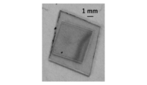
- 1 is a planar image of composite 1 of Example 1 observed from the diamond substrate side.
- 1 is a planar image of composite 2 of Example 1 observed from the GaN layer side.
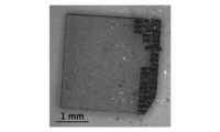
- 1 is a planar image of the composite of Example 2 observed from the diamond substrate side.
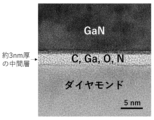
- 1 is a cross-sectional microscope image of the composite of Example 2.
- 1 is a transmission electron microscope image of the bonding interface of the composite of Example 2.
- 13 is an energy dispersive X-ray spectroscopy spectrum of the intermediate layer of the composite of Example 2.
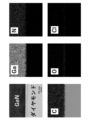
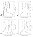
- 4 is a transmission electron microscope image and element map of the vicinity of the bonded interface of the composite of Example 2. Electron energy loss spectroscopy spectra of the intermediate layer of the composite of Example 2 and the diamond substrate.
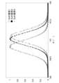
- 13 is a planar image of the adhesion body of Comparative Example 2 observed from the diamond substrate side. 13 is a planar image of the adhesion body of Comparative Example 3 observed from the diamond substrate side. 1 is a planar image of the composite of Example 3 observed from the diamond substrate side. 13 is a planar image of the composite of Example 4 observed from the diamond wafer side. 4 is a rocking curve of a GaN substrate of a reference example. 4 shows X-ray photoelectron spectroscopy spectra of the surface of the GaN layer before and after the reduction treatment in Example 2.
- the composite of the embodiment of the present application includes a gallium nitride layer, an intermediate layer, and a diamond layer.
- the intermediate layer is formed on the surface of the gallium nitride layer.
- the diamond layer is bonded to the surface of the gallium nitride layer via the intermediate layer. More specifically, a second substrate containing a diamond layer is bonded to a first substrate containing a gallium nitride layer via the intermediate layer.
- the intermediate layer contains carbon, gallium, and oxygen.
- the intermediate layer may contain nitrogen.
- the first substrate examples include various substrates such as a single crystal GaN substrate, a GaN/sapphire substrate having a GaN layer on the surface of a sapphire substrate, a GaN/Si substrate having a GaN layer on the surface of a Si substrate, and a GaN/SiC substrate having a GaN layer on the surface of a SiC substrate.
- a natural oxide film which is a gallium oxide film, is formed on the surface of these GaN layers, and in this embodiment, the intermediate layer is derived from this gallium oxide film.
- the intermediate layer may be derived from a gallium oxide film other than the natural oxide film on the GaN layer.
- the fact that the intermediate layer contains gallium oxide can be determined by energy dispersive X-ray analysis.
- the thickness of the intermediate layer is preferably 4 nm or less. Since the thickness of the natural oxide film formed on the surface of the GaN layer is approximately 2 nm, the thickness of the intermediate layer is often 2 nm or more.
- the nitrogen content is greater than the oxygen content.
- sputtering the natural oxide film causes the crystallinity of the GaN to deteriorate.
- the intermediate layer is derived from the gallium oxide film on the surface of the GaN layer. Therefore, the oxygen content of the intermediate layer is greater than the nitrogen content.
- the first substrate and the second substrate are bonded via an intermediate layer that contains carbon, gallium, and oxygen and has a smaller nitrogen content than the oxygen content, so that the shear strength between the first substrate and the second substrate is 0.1 MPa or more.
- the second substrate may be a single crystal diamond substrate, a diamond/Si substrate having a diamond layer on the surface of a Si substrate, or a diamond/sapphire substrate having a diamond layer on the surface of a sapphire substrate.
- the diamond layer preferably has a surface of the (100) or (111) plane.
- the diamond layer may also be a mosaic crystal having a surface of the (100) or (111) plane.
- the manufacturing method of the composite of the first embodiment of the present application includes a first substrate treatment step, a second substrate treatment step, and a bonding step.
- the first substrate includes a gallium nitride layer and an exposed gallium oxide layer formed on the gallium nitride layer.
- a predetermined treatment is applied to the surface of the gallium oxide layer of the first substrate to functionalize the surface of the gallium oxide layer.
- the predetermined treatment is one or more of an oxidation treatment, a nitridation treatment, and a reduction treatment.
- the oxidation treatment is a treatment in which oxygen atoms are introduced into the surface of the gallium oxide layer to grow the gallium oxide layer.
- the nitridation treatment is a treatment in which nitrogen atoms are introduced into the surface of the gallium oxide layer.
- the reduction treatment is a treatment in which reactive functional groups are introduced into the surface while thinning the gallium oxide layer.
- Examples of the oxidation treatment include treatment with a liquid containing ammonia and hydrogen peroxide, and treatment with reactive oxygen plasma.
- Examples of the nitridation treatment include treatment with reactive nitrogen plasma.
- Examples of the reduction treatment include treatment with hydrochloric acid.
- the treatment with hydrochloric acid functionalizes the surface of the gallium oxide layer with one or more of -OH groups, -NH2 groups, and -Cl groups.
- the second substrate has a diamond layer whose surface is a (111) plane.
- an oxidation treatment is performed on the surface of the diamond layer of the second substrate to introduce oxygen atoms into the surface of the diamond layer and functionalize the surface of the diamond layer.
- the oxidation treatment forms C-O-C groups or -OH groups on the surface of the diamond layer.
- the surface of this functionalized diamond layer has properties that make it easy to bond with the surface of the gallium oxide layer functionalized in the first substrate treatment step.
- the surface of the gallium oxide layer that has undergone the first substrate treatment process is brought into contact with the surface of the diamond layer that has undergone the second substrate treatment process, and reactive energy is applied to this contact area to bond the first substrate and the second substrate.
- reactive energy include thermal energy, light energy, electrical energy, and chemical energy.
- the contact area between the first substrate and the second substrate is heated to a temperature of approximately 200°C.
- the bonding process bonds the surfaces of the gallium oxide layer and the diamond layer together. According to electron energy loss spectroscopy of the gallium oxide layer and diamond layer after bonding, it is believed that the gallium oxide layer and diamond layer are not bonded by the formation of Ga-O-C bonds, but are bonded by the diffusion of C atoms on the surface of the diamond layer into the gallium oxide layer.
- the bonding process can be carried out in a vacuum container, but can also be carried out in the atmosphere. Therefore, a vacuum bonding device is not required for the bonding process in the manufacturing method of the composite of this embodiment.
- the method for manufacturing a composite according to this embodiment also includes a first substrate treatment step, a second substrate treatment step, and a bonding step.
- a nitriding treatment is performed on the surface of the gallium oxide layer of the first substrate, which includes a gallium nitride layer and an exposed gallium oxide layer formed on the gallium nitride layer, to functionalize the surface of the gallium oxide layer.
- an oxidation treatment is performed on the surface of the diamond layer of the second substrate, which includes a diamond layer whose surface is a (100) plane, to functionalize the surface of the diamond layer.
- Diamonds with a (100) surface are commonly used in industry. However, it has been difficult to bond (100) diamond to GaN.
- the inventors of the present application have discovered that by subjecting the gallium oxide layer on the gallium nitride layer to a nitriding treatment, rather than an oxidation and reduction treatment, it becomes easier to bond to the oxidized (100) diamond surface.
- the surface of the gallium oxide layer that has been subjected to the first substrate treatment process and the surface of the diamond layer that has been subjected to the second substrate treatment process are brought into contact with each other, and reaction energy is applied to this contact portion to bond the first substrate and the second substrate.
- Example 1 A GaN/sapphire substrate (POWDEC, thickness 0.635 mm) having a 2 ⁇ m thick GaN layer on the sapphire substrate surface, the (0001) surface of which was polished, was cut into a parallelogram shape with one side of about 8 mm and the adjacent side of about 7 mm.
- the surface of the GaN layer of this GaN/sapphire substrate was treated by the following procedure.
- the surface of this GaN layer i.e., the native oxide layer of GaN, was immersed for 10 minutes in a treatment solution at a liquid temperature of 75° C., which was composed of 10 mL of 28% ammonia water, 10 mL of 35% hydrogen peroxide water, and 50 mL of pure water.
- the surface of this GaN layer was then washed with pure water for 5 minutes (oxidation treatment).
- the surface of the diamond layer of a single crystal diamond substrate (EDP Corporation) with a (111) surface, a thickness of 0.3 mm, and a size of 3 mm square was treated under the same conditions as the surface treatment of the GaN layer (oxidation treatment). These oxidation treatments functionalized the surfaces of the GaN layer and the diamond layer, making them more easily bonded to each other. After leaving the surfaces of the GaN layer and the diamond layer in contact in the atmosphere for one day, they were heated at a temperature of 200°C for two hours to obtain a composite 1 in which the GaN/sapphire substrate and the diamond substrate were bonded, i.e., the GaN layer and the diamond layer were bonded.
- FIG. 1 is a planar image of the composite 1 observed from the diamond substrate side. As shown in FIG. 1, no bright areas indicating depletion between the substrates were observed. That is, most of the surface of the GaN layer of the GaN/sapphire substrate and the surface of the diamond layer of the diamond substrate were bonded.
- FIG. 2 is a planar image of the composite 2 observed from the GaN layer side. As shown in FIG. 2, a plurality of rectangular GaN layers of 0.3 mm ⁇ 0.15 mm were formed in the right region of the surface of the 3 mm square diamond substrate. The thickness of this GaN layer was 2 ⁇ m.
- Example 2 A GaN/Si substrate (CoorsTek, thickness 0.635 mm) having a 2 ⁇ m thick GaN layer on the surface of a Si substrate, the (0001) surface of which was polished, was cut into a 15 mm ⁇ 16 mm rectangular shape.
- the surface of the GaN layer of this GaN/Si substrate was treated by the following procedure.
- the surface of this GaN layer i.e., the native oxide layer of GaN, was immersed for 10 minutes in a treatment solution at a liquid temperature of 70° C., which was composed of 10 mL of 35% hydrochloric acid and 60 mL of pure water.
- the surface of this GaN layer was then washed with pure water for 5 minutes (reduction treatment).
- FIG. 14 shows the X-ray photoelectron spectroscopy spectrum of the surface of the GaN layer after this reduction treatment ("HCl treatment” in the figure) and the surface of the GaN layer before this reduction treatment ("untreated” in the figure).
- HCl treatment in the figure
- untreated in the figure.
- the peak derived from the O1s orbital becomes smaller and the position of this peak moves to the higher energy side.
- the reduction treatment of the surface of the GaN layer makes the native oxide layer on the surface of the GaN layer thinner, and Ga-OH, which has a higher bond energy than Ga 2 O 3, is formed.
- the peak derived from -NH 2 group near 397.7 eV and the peak derived from -Cl group near 200 eV become larger. It can be seen that Ga-NH 2 and Ga-Cl are formed.
- a surface-treated diamond substrate was obtained under the same conditions as in Example 1, except that the temperature of the treatment solution during immersion was changed to 70°C (oxidation treatment). It is known that C-O-C or C-OH is formed on the surface of a diamond layer that has been subjected to oxidation treatment. Thereafter, a composite was obtained in which the GaN layer of the GaN/Si substrate and the diamond layer of the diamond substrate were bonded together, by the same method as in Example 1. This composite was obtained by reacting at the interface between the -OH group, -NH2 group, or -Cl group formed on the surface of the GaN layer and the C-O-C group or -OH group formed on the surface of the diamond layer.
- Figure 3 is a planar image of this composite when observed from the diamond substrate side.
- this composite has the surfaces of the diamond layers of two small diamond substrates bonded to the surface of the GaN layer of a large GaN/Si substrate. Even though the GaN layer and diamond layer overlap, Newton's rings are observed in the areas where the surfaces of the GaN layer and diamond layer are not bonded.
- the surface of the diamond layer of the diamond substrate in the upper right is bonded entirely to the surface of the GaN layer, and the surface of the diamond layer of the diamond substrate in the lower center is bonded to approximately 70% of the surface area of the GaN layer.
- FIG 4 is a microscope image of this cross section. As shown in Figure 4, no non-bonded areas were observed at the bonding interface between the diamond layer and the GaN layer of the diamond substrate. In addition, this composite was irradiated with laser light to cut it, and an extremely thin specimen was produced by irradiating the cross section with a focused ion beam. The bonding interface between the diamond layer and the GaN layer of this specimen was observed using a transmission electron microscope.
- Figure 5 is a transmission electron microscope image of this bonding interface. As shown in Figure 5, an intermediate layer with a thickness of approximately 3 nm was observed at the bonding interface.
- the composition of this intermediate layer was analyzed by energy dispersive X-ray spectroscopy.
- Figure 6 shows the energy dispersive X-ray spectrum of this intermediate layer.
- the element ratio of this intermediate layer was C: 59.8%, Ga: 28.0%, O: 9.4%, N: 2.8%, Cl: 0.1%, and the O content was greater than the N content.
- element mapping was performed near the bonding interface of this sample by energy dispersive X-ray spectroscopy.
- Figure 7 shows a transmission electron microscope image of the bonding interface of this sample and element maps of C, Ga, O, N, and Cl.
- the GaN layer portion is composed of Ga and N
- the diamond layer portion is composed of C
- small amounts of O and Cl were observed at the bonding interface.
- Figure 8 shows the electron energy loss spectroscopy spectra of the intermediate layer and the diamond layer of this sample for C, Ga, O, and N.
- a peak derived from the ⁇ bond (sp 3 ) of carbon is observed around 292 eV.
- a ⁇ bond peak was observed inside the diamond layer of this sample (inside the diamond in the figure), but a peak characteristic of the ⁇ bond (sp 2 ) was observed around 286 eV at the interface between the intermediate layer and the diamond layer (interface intermediate layer/diamond in the figure).
- the intermediate layer is composed of sp 2 bonded carbon, gallium, and oxygen.
- Comparative Example 1 The surface of the GaN layer of the same GaN/sapphire substrate as in Example 1 and the surface of the diamond layer of the same single crystal diamond substrate as in Example 1 were washed with acetone, ethanol, and pure water in that order for 5 minutes each. The washed surfaces of the GaN/sapphire substrate and the diamond substrate were left in contact with each other in the atmosphere for 1 day, and then heated at a temperature of 200°C for 2 hours. However, the GaN layer of the GaN/sapphire substrate and the diamond layer of the single crystal diamond substrate were not bonded.
- Example 1 the surface treatment with acetone, ethanol, and pure water, which does not correspond to the oxidation treatment, nitridation treatment, and reduction treatment, did not change the properties of the GaN layer and the diamond substrate to be easily bonded to each other.
- Comparative Example 2 The same GaN/sapphire substrate as in Example 1 was cut into a parallelogram shape with one side of about 8 mm and the adjacent side of about 7 mm.
- the surface of the GaN layer of this GaN/sapphire substrate was treated (reduction treatment) under the same conditions as the surface treatment of the GaN layer of the GaN/sapphire substrate in Example 2.
- the surface of the diamond layer of a single crystal diamond substrate (EDP Corporation) with a (100) surface, a thickness of 0.3 mm, and a size of 5 mm square was treated (oxidation treatment) under the same conditions as the surface treatment of the diamond layer of the diamond substrate in Example 1.
- FIG. 9 is a planar image of this attachment observed from the diamond substrate side. As shown in Figure 9, the depletion between the GaN/sapphire substrate and the diamond substrate was bright, and Newton's rings were observed, indicating that the GaN layer and diamond layer of this attachment were not bonded completely.
- Comparative Example 3 The same GaN/sapphire substrate as in Example 1 was cut into a parallelogram shape with one side of about 8 mm and the adjacent side of about 7 mm. The surface of the GaN layer of this GaN/sapphire substrate was treated under the same conditions as the surface treatment of the GaN layer of the GaN/sapphire substrate in Example 1 (oxidation treatment). Meanwhile, the surface of the diamond layer of the same diamond substrate as in Comparative Example 2 was subjected to reactive ion etching treatment (oxidation treatment) using oxygen gas at a pressure of 40 Pa at a power of 200 W for 30 seconds.
- oxidation treatment reactive ion etching treatment
- FIG. 10 is a planar image of this attachment observed from the diamond substrate side. As shown in Figure 10, the depletion between the GaN/sapphire substrate and the diamond substrate was bright, and Newton's rings were observed, indicating that the GaN layer and the diamond layer were not bonded completely. Furthermore, this attachment broke when a shear strength of 48 kPa was applied.
- Example 3 The same GaN/sapphire substrate as in Example 1 was cut into a parallelogram shape with one side of about 8 mm and the adjacent side of about 7 mm.
- the surface of the GaN layer of this GaN/sapphire substrate was treated under the same conditions as the surface treatment of the GaN layer of the GaN/sapphire substrate in Example 1. Furthermore, the surface of this GaN layer was treated by reactive ion etching using nitrogen gas at a pressure of 40 Pa and an output of 200 W for 30 seconds (nitridation treatment). Meanwhile, the surface of the diamond layer of the same diamond substrate as in Comparative Example 2 was treated under the same conditions as the surface treatment of the diamond layer of the diamond substrate in Example 1 (oxidation treatment).
- FIG. 11 is a planar image of this composite observed from the diamond substrate side. Darkness due to depletion between the substrates was only observed in a part of the right side of the diamond substrate. In other words, in this composite, the substrates were bonded together, i.e., the GaN layer and the diamond layer were mostly bonded together. This composite broke when a shear strength of 2.8 MPa was applied.
- Example 4 The same GaN/sapphire substrate as in Example 1 was cut into a rectangular shape of 15 mm x 16 mm. Thereafter, a GaN/sapphire substrate was obtained in which the surface of the GaN layer was nitrided in the same manner as in Example 3. Meanwhile, the surface of the diamond layer of a circular mosaic single crystal diamond minimal wafer (EDP Co., Ltd.) with a (100) surface, a thickness of 0.3 mm and a diameter of 12.5 mm was treated (oxidation treatment) under the same conditions as the surface treatment of the diamond layer of the diamond substrate in Example 1.
- EDP Co., Ltd. circular mosaic single crystal diamond minimal wafer
- FIG. 12 is a planar image of this composite observed from the diamond wafer side. Darkness due to depletion between the substrate and wafer was only observed in a small area at the top left of the center of the diamond wafer. In other words, most of the GaN layer and diamond layer were bonded together in this composite.
- Example 2 The surface of the GaN layer of the same GaN/sapphire substrate as in Example 1 was irradiated for 120 seconds with an Ar atomic beam accelerated at a voltage of 1.5 kV and a current of 100 mA, to obtain a GaN substrate 1 in which the surface oxide film of the GaN layer was sputtered off.
- a GaN substrate 2 was obtained in which the surface of the GaN layer was subjected to a reduction treatment in the same manner as in Example 2.
- a GaN substrate 3 was obtained in which the surface of the GaN layer was subjected to a nitriding treatment in the same manner as in Example 3.
- Figure 13 shows the results of rocking curve measurement of each GaN substrate by XRD.
- the half-width of the in-plain XRD was 0.333°, and the half-width of the rocking curve measurement was 0.418°.
- the half-width of the in-plain XRD was 0.331°, and the half-width of the rocking curve measurement was 0.395°.
- the half-width of the in-plain XRD was 0.330°, and the half-width of the rocking curve measurement was 0.387°.
- the surface oxide film of the GaN layer to the oxidation treatment, nitridation treatment, and reduction treatment of the present application, the deterioration of the crystallinity of the surface of the GaN layer can be suppressed while changing the properties of the surface of the GaN layer to one that makes it easier to bond to the surface of the diamond layer.
Landscapes
- Chemical & Material Sciences (AREA)
- Engineering & Computer Science (AREA)
- Crystallography & Structural Chemistry (AREA)
- Materials Engineering (AREA)
- Metallurgy (AREA)
- Organic Chemistry (AREA)
- Ceramic Engineering (AREA)
- Inorganic Chemistry (AREA)
- Mechanical Engineering (AREA)
- Crystals, And After-Treatments Of Crystals (AREA)
- Laminated Bodies (AREA)
- Formation Of Insulating Films (AREA)
- Pressure Welding/Diffusion-Bonding (AREA)
Abstract
GaNとダイヤモンドの結晶性の劣化を抑えつつ、大気中でもこれらを接合できる複合体の製造方法を提供する。GaNとダイヤモンドが接合された複合体の製造方法は、窒化ガリウム層と、窒化ガリウム層上に形成され、露出した酸化ガリウム層を備える第一基材の酸化ガリウム層の表面に、酸化処理、窒化処理、および還元処理の一つ以上の処理を施して、酸化ガリウム層の表面を官能基化する第一基材処理工程と、表面が(111)面であるダイヤモンド層を備える第二基材のダイヤモンド層の表面に酸化処理を施して、ダイヤモンド層の表面を官能基化する第二基材処理工程と、第一基材処理工程を経た酸化ガリウム層の表面と、第二基材処理工程を経たダイヤモンド層の表面を接触させた状態で、この接触部に反応エネルギーを与えて、第一基材と第二基材を接合する接合工程を有する。
Description
本願は、窒化ガリウムとダイヤモンドが、炭素、ガリウム、および酸素を含有する中間層を介して接合された複合体とその製造方法に関する。
次世代パワー半導体の基板素材として窒化ガリウム(GaN)が着目されている。そして、GaNの放熱性能を向上させるため、GaN系半導体がダイヤモンド基板に直接接合された半導体デバイスが知られている(特許文献1)。特許文献1では、GaNとダイヤモンドを接合する各表面にアルゴンビームを照射し、自然酸化膜などを除去して活性化した後、圧力10-6Pa以下の真空容器内で、GaNとダイヤモンドを直接接合している。
特許文献1の接合方法では、GaN表面へのアルゴンビーム照射によって、GaNの結晶性が劣化してしまう。GaNの結晶性が劣化すると、GaN系半導体のデバイスとしての特性が低下する。また、ダイヤモンド表面へのアルゴンビーム照射によって、ダイヤモンドの結晶性も劣化する。ダイヤモンドは電気絶縁破壊電界が高く、GaN系半導体の絶縁担保に適切である。しかし、結晶性が劣化したダイヤモンドは電気絶縁性が低い。このため、結晶性が劣化したダイヤモンドをGaN系半導体に接合すると、GaN系半導体の動作に悪影響を及ぼす。また、特許文献1の接合方法は、高真空中で行うため、真空接合装置が必要となる。
本願は、このような事情に鑑みてなされたものであり、GaNとダイヤモンドの結晶性の劣化を抑えつつ、大気中でもこれらを接合できる複合体の製造方法と、結晶性の劣化が抑えられたダイヤモンドが、中間層を介して、結晶性の劣化が抑えられたGaNに接合している複合体を提供することを課題とする。
本願の複合体は、窒化ガリウム層と、窒化ガリウム層の表面に形成され、炭素、ガリウム、および酸素を含有する中間層と、中間層を介して、窒化ガリウム層の表面に接合されているダイヤモンド層を有する。
本願のある態様の複合体の製造方法は、窒化ガリウム層と、窒化ガリウム層上に形成され、露出した酸化ガリウム層を備える第一基材の酸化ガリウム層の表面に、酸化処理、窒化処理、および還元処理の一つ以上の処理を施して、酸化ガリウム層の表面を官能基化する第一基材処理工程と、表面が(111)面であるダイヤモンド層を備える第二基材のダイヤモンド層の表面に酸化処理を施して、ダイヤモンド層の表面を官能基化する第二基材処理工程と、第一基材処理工程を経た酸化ガリウム層の表面と、第二基材処理工程を経たダイヤモンド層の表面を接触させた状態で、この接触部に反応エネルギーを与えて、第一基材と第二基材を接合する接合工程を有する。
本願の他の態様の複合体の製造方法は、窒化ガリウム層と、窒化ガリウム層上に形成され、露出した酸化ガリウム層を備える第一基材の酸化ガリウム層の表面に、窒化処理を施して、酸化ガリウム層の表面を官能基化する第一基材処理工程と、表面が(100)面であるダイヤモンド層を備える第二基材のダイヤモンド層の表面に酸化処理を施して、ダイヤモンド層の表面を官能基化する第二基材処理工程と、第一基材処理工程を経た酸化ガリウム層の表面と、第二基材処理工程を経たダイヤモンド層の表面を接触させた状態で、この接触部に反応エネルギーを与えて、第一基材と第二基材を接合する接合工程を有する。
本願の複合体の製造方法では、窒化ガリウム層上の酸化ガリウム層と、ダイヤモンド層に、結晶性の劣化を抑えた所定の処理をそれぞれ施して官能基化し、接合している。このため、本願の複合体の製造方法によれば、結晶性の劣化が抑えられた窒化ガリウム層とダイヤモンド層が接合された複合体が得られる。また、本願の複合体は、窒化ガリウム層とダイヤモンド層が、所定の中間層を介して接合されている。このため、本願の複合体によれば、結晶性の劣化が抑えられた窒化ガリウム層とダイヤモンド層が接合された複合体が得られる。
本願の実施形態の複合体は、窒化ガリウム層と、中間層と、ダイヤモンド層を備えている。中間層は、窒化ガリウム層の表面に形成されている。ダイヤモンド層は、中間層を介して、窒化ガリウム層の表面に接合されている。より具体的には、中間層を介して、窒化ガリウム層を含有する第一基材に、ダイヤモンド層を含有する第二基材が接合されている。中間層は、炭素、ガリウム、および酸素を含有している。中間層に窒素が含有されていてもよい。第一基材としては、単結晶GaN基板、GaN層をサファイア基材表面に有するGaN/サファイア基板、GaN層をSi基材表面に有するGaN/Si基板、およびGaN層をSiC基材表面に有するGaN/SiC基板などの各種基板が挙げられる。
これらのGaN層の表面には、酸化ガリウム膜である自然酸化膜が形成されており、本実施形態では、中間層がこの酸化ガリウム膜に由来する。なお、中間層は、GaN層上の自然酸化膜以外の酸化ガリウム膜に由来していてもよい。中間層が酸化ガリウムを含有していることは、エネルギー分散型X線分析によって判定できる。窒化ガリウム層とダイヤモンド層の間の熱伝導性の低下を抑えるため、中間層の厚さは4nm以下であることが好ましい。GaN層の表面に形成される自然酸化膜の厚さが約2nmであることから、中間層の厚さは、2nm以上となる場合が多い。
特許文献1の超高真空中のスパッタ処理にて自然酸化膜を除去して接合した半導体デバイスのGaN系半導体とダイヤモンド基板の接合界面では、窒素含有量が酸素含有量より大きい。しかしながら、自然酸化膜をスパッタ処理すると、GaNの結晶性が劣化してしまう。本実施形態では、中間層がGaN層の表面の酸化ガリウム膜に由来する。このため、中間層の酸素含有量は窒素含有量より大きくなる。このように、炭素、ガリウム、および酸素を含有し、窒素含有量が酸素含有量より小さい中間層を介して第一基材と第二基材が接合されることによって、第一基材と第二基材の間のせん断強度が0.1MPa以上となる。
第二基材としては、単結晶ダイヤモンド基板、ダイヤモンド層をSi基材表面に有するダイヤモンド/Si基板、およびダイヤモンド層をサファイア基材表面に有するダイヤモンド/サファイア基板などの各種基板が挙げられる。ダイヤモンド層は、(100)面または(111)面の表面を備えていることが好ましい。また、ダイヤモンド層は、(100)面または(111)面の表面を備えているモザイク結晶であってもよい。
本願の第一実施形態の複合体の製造方法は、第一基材処理工程と、第二基材処理工程と、接合工程を備えている。第一基材は、窒化ガリウム層と、この窒化ガリウム層上に形成され、露出した酸化ガリウム層を備えている。第一基材処理工程では、第一基材の酸化ガリウム層の表面に所定の処理を施して、酸化ガリウム層の表面を官能基化する。この所定の処理は、酸化処理、窒化処理、および還元処理の一つ以上の処理である。
この酸化処理は、酸化ガリウム層の表面に酸素原子を導入し、酸化ガリウム層を成長させる処理である。この窒化処理は、酸化ガリウム層の表面に窒素原子を導入する処理である。この還元処理は、酸化ガリウム層を薄くしながら、表面に反応性の官能基を導入する処理である。酸化処理としては、アンモニアと過酸化水素を含有する液体での処理、および反応性酸素プラズマでの処理が挙げられる。窒化処理としては、反応性窒素プラズマでの処理が挙げられる。還元処理としては、塩酸での処理が挙げられる。この塩酸での処理によって、酸化ガリウム層の表面が-OH基、-NH2基、および-Cl基の一種以上に官能基化される。
これらの各種処理の例示は、第一実施形態の複合体の製造方法における第二基材処理工程、ならびに第二実施形態の複合体の製造方法における第一基材処理工程および第二基材処理工程でも同様である。第一基材処理工程で酸化処理または窒化処理によって官能基化された酸化ガリウム層の表面がどのような化学構造であるかは、必ずしも明らかでない。しかし、官能基化された酸化ガリウム層の表面は、第二基材処理工程で官能基化されたダイヤモンド層の表面と接合しやすい性状になっている。しかも、酸化ガリウム層の全体除去を伴わないこれらの所定の処理によって、GaN層の結晶性の劣化を抑えている。
第二基材は、表面が(111)面であるダイヤモンド層を備えている。第二基材処理工程では、第二基材のダイヤモンド層の表面に酸化処理を施して、ダイヤモンド層の表面に酸素原子を導入し、ダイヤモンド層の表面を官能基化する。酸化処理によって、ダイヤモンド層の表面には、C-O-C基または-OH基が形成される。この官能基化されたダイヤモンド層の表面は、第一基材処理工程で官能基化された酸化ガリウム層の表面と接合しやすい性状になっている。
接合工程では、第一基材処理工程を経た酸化ガリウム層の表面と、第二基材処理工程を経たダイヤモンド層の表面を接触させた状態で、この接触部に反応エネルギーを与えて、第一基材と第二基材を接合する。反応エネルギーとしては、熱エネルギー、光エネルギー、電気エネルギー、または化学エネルギーなどが挙げられる。本実施形態では、温度約200℃で、第一基材と第二基材の接触部を加熱する。
接合工程によって、酸化ガリウム層とダイヤモンド層の表面同士が接合する。接合後の酸化ガリウム層とダイヤモンド層の電子エネルギー損失分光スペクトルによれば、酸化ガリウム層とダイヤモンド層は、Ga-O-C結合の形成によって接合されているのではなく、ダイヤモンド層の表面のC原子が酸化ガリウム層に拡散することによって接合されていると考えられる。なお、接合工程は、真空容器内でも行えるが、大気中でも行える。このため、本実施形態の複合体の製造方法における接合工程では、真空接合装置が不要である。
本願の第二実施形態の複合体の製造方法について説明する。本実施形態の複合体の製造方法の説明では、第一実施形態の複合体の製造方法との重複を適宜省略する。本実施形態の複合体の製造方法も、第一基材処理工程と、第二基材処理工程と、接合工程を備えている。第一基材処理工程では、窒化ガリウム層と、窒化ガリウム層上に形成され、露出した酸化ガリウム層を備える第一基材の酸化ガリウム層の表面に、窒化処理を施して、酸化ガリウム層の表面を官能基化する。第二基材処理工程では、表面が(100)面であるダイヤモンド層を備える第二基材のダイヤモンド層の表面に酸化処理を施して、ダイヤモンド層の表面を官能基化する。
表面が(100)面であるダイヤモンド(以下単に「(100)ダイヤモンド」と記載することがある)は、産業界で一般的に使用されている。しかし、(100)ダイヤモンドとGaNを接合するのは困難であった。本願発明者は、窒化ガリウム層上の酸化ガリウム層を、酸化処理および還元処理ではなく、窒化処理することによって、酸化処理した(100)ダイヤモンド表面と接合しやすくなることを見出した。接合工程では、第一実施形態の複合体の製造方法における接合工程と同様に、第一基材処理工程を経た酸化ガリウム層の表面と、第二基材処理工程を経たダイヤモンド層の表面を接触させた状態で、この接触部に反応エネルギーを与えて、第一基材と第二基材を接合する。
実施例1
(0001)面である表面が研磨された厚さ2μmのGaN層をサファイア基材表面に有するGaN/サファイア基板(POWDEC社、厚さ0.635mm)を、一辺が約8mmで、その隣の一辺が約7mmの平行四辺形状に切断した。このGaN/サファイア基板のGaN層の表面を以下の手順で処理した。28%アンモニア水10mL、35%過酸化水素水10mL、および純水50mLから構成される液温75℃の処理液に、このGaN層の表面、すなわちGaNの自然酸化膜層を10分間浸漬した。その後、純水によりこのGaN層の表面を5分間洗浄した(酸化処理)。
(0001)面である表面が研磨された厚さ2μmのGaN層をサファイア基材表面に有するGaN/サファイア基板(POWDEC社、厚さ0.635mm)を、一辺が約8mmで、その隣の一辺が約7mmの平行四辺形状に切断した。このGaN/サファイア基板のGaN層の表面を以下の手順で処理した。28%アンモニア水10mL、35%過酸化水素水10mL、および純水50mLから構成される液温75℃の処理液に、このGaN層の表面、すなわちGaNの自然酸化膜層を10分間浸漬した。その後、純水によりこのGaN層の表面を5分間洗浄した(酸化処理)。
一方、表面が(111)面であり、厚さ0.3mmで3mm角の単結晶ダイヤモンド基板(イーディーピー社)のダイヤモンド層の表面を、GaN層の表面処理と同じ条件で処理した(酸化処理)。これらの酸化処理によって、GaN層の表面とダイヤモンド層の表面が官能基化され、これらの表面同士が接合しやすい性状になった。大気中でこのGaN層の表面とこのダイヤモンド層の表面を接触させたまま1日間経過させた後、温度200℃で2時間加熱して、GaN/サファイア基板とダイヤモンド基板が接合された、すなわちGaN層とダイヤモンド層が接合された複合体1を得た。
図1は、複合体1をダイヤモンド基板側から観察したときの平面画像である。図1に示すように、基板間の空乏を示す明るい部分が観察されなかった。すなわち、GaN/サファイア基板のGaN層の表面とダイヤモンド基板のダイヤモンド層の表面の大部分が接合されていた。複合体1のサファイア基材側から、波長248nm、エネルギー密度1000mJ/cm2のレーザー光を0.3mm×0.15mmの格子状に照射して、GaN/サファイア基板からGaN層を剥離してダイヤモンド基板のダイヤモンド層の表面に転写し、ダイヤモンド層がGaN層に接合された複合体2を得た。図2は、複合体2をGaN層側から観察したときの平面画像である。図2に示すように、3mm角のダイヤモンド基板表面の右側領域に、0.3mm×0.15mmの長方形状の複数のGaN層が形成されていた。なお、このGaN層の厚さは2μmであった。
実施例2
(0001)面である表面が研磨された厚さ2μmのGaN層をSi基材表面に有するGaN/Si基板(クアーズテック社、厚さ0.635mm)を、15mm×16mmの長方形状に切断した。このGaN/Si基板のGaN層の表面を以下の手順で処理した。35%塩酸10mLおよび純水60mLから構成される液温70℃の処理液に、このGaN層の表面、すなわちGaNの自然酸化膜層を10分間浸漬した。その後、純水によりこのGaN層の表面を5分間洗浄した(還元処理)。
(0001)面である表面が研磨された厚さ2μmのGaN層をSi基材表面に有するGaN/Si基板(クアーズテック社、厚さ0.635mm)を、15mm×16mmの長方形状に切断した。このGaN/Si基板のGaN層の表面を以下の手順で処理した。35%塩酸10mLおよび純水60mLから構成される液温70℃の処理液に、このGaN層の表面、すなわちGaNの自然酸化膜層を10分間浸漬した。その後、純水によりこのGaN層の表面を5分間洗浄した(還元処理)。
この還元処理を経たGaN層の表面(図中「HCl処理」)とこの還元処理前のGaN層の表面(図中「未処理」)のX線高電子分光スペクトルを図14に示す。図14に示すように、GaN層の表面を塩酸で処理することで、O1s軌道に由来するピークが小さくなるとともに、このピーク位置が高エネルギー側に移動している。GaN層の表面の還元処理によって、GaN層の表面の自然酸化膜層が薄くなり、Ga2O3よりも結合エネルギーが大きいGa-OHが形成されたことが分かる。さらに、397.7eV付近の-NH2基に由来するピークと、200eV付近の-Cl基に由来するピークが大きくなった。Ga-NH2とGa-Clが形成されているのが分かる。
一方、浸漬時の処理液の温度を70℃に変更した点を除いて実施例1と同じ条件で、表面処理されたダイヤモンド基板を得た(酸化処理)。酸化処理を施したダイヤモンド層の表面には、C-O-CまたはC-OHが形成されることが知られている。その後は実施例1と同じ方法によって、GaN/Si基板のGaN層とダイヤモンド基板のダイヤモンド層が接合された複合体を得た。GaN層の表面に形成された-OH基、-NH2基、または-Cl基と、ダイヤモンド層の表面に形成されたC-O-C基または-OH基が界面で反応してこの複合体が得られた。
図3は、この複合体をダイヤモンド基板側から観察したときの平面画像である。図3に示すように、この複合体は、大きなGaN/Si基板のGaN層の表面に、2つの小さなダイヤモンド基板のダイヤモンド層の表面が接合されている。GaN層とダイヤモンド層が重なっていても、GaN層の表面とダイヤモンド層の表面が接合されていない部分にはニュートンリングが観察される。図3に示すように、右上のダイヤモンド基板のダイヤモンド層の表面は、GaN層の表面に全面的に接合されており、中央下のダイヤモンド基板のダイヤモンド層の表面は、GaN層の表面の約70%の領域に接合されていた。
レーザー光を照射して、ダイヤモンド基板、GaN層、およびSi基板を通るように、この複合体を切断した。図4はこの断面の顕微鏡像である。図4に示すように、ダイヤモンド基板のダイヤモンド層とGaN層の接合界面には非接合部が観察されなかった。また、この複合体にレーザー光を照射して切断し、断面への集束イオンビーム照射により極薄の試料を作製した。この試料のダイヤモンド層とGaN層の接合界面を透過型電子顕微鏡により観察した。図5はこの接合界面の透過型電子顕微鏡像である。図5に示すように、接合界面には厚さ約3nmの中間層が観察された。
エネルギー分散型X線分光法により、この中間層の組成を分析した。図6は、この中間層のエネルギー分散型X線分光スペクトルである。この中間層の元素比は、C:59.8%、Ga:28.0%、O:9.4%、N:2.8%、Cl:0.1%であり、O含有量>N含有量となっていた。さらに、この試料の接合界面付近について、エネルギー分散型X線分光法による元素マッピングを行った。図7は、この試料の接合界面付近の透過型電子顕微鏡像と、C、Ga、O、N、およびClの各元素マップである。GaN層部分はGaとNから構成され、ダイヤモンド層部分はCから構成され、接合界面では少量のOとClが観測された。
また、電子エネルギー損失分光(EELS)により、この試料の中間層とダイヤモンド層の構造を評価した。図8は、C、Ga、O、およびNについてのこの試料の中間層とダイヤモンド層の電子エネルギー損失分光スペクトルである。ダイヤモンドの結晶性が高い領域では、292eV近辺に炭素のσ結合(sp3)に由来するピークが観測される。この試料のダイヤモンド層内部(図中「ダイヤモンド内部」)ではσ結合のピークが観測されたが、中間層とダイヤモンド層の界面(図中「界面中間層/ダイヤモンド」)では286eV近辺のπ結合(sp2)に特徴的なピークが観測された。また、ダイヤモンド層内部と中間層内部(図中「界面中間層内部」)では、GaとOのピークは検出されたが、Nについては有意なピークが検出されなかった。これらの結果から、中間層は、sp2結合の炭素、ガリウム、および酸素から構成されていると考えられる。
比較例1
実施例1と同じGaN/サファイア基板のGaN層の表面と、実施例1と同じ単結晶ダイヤモンド基板のダイヤモンド層の表面を、アセトン、エタノール、および純水の順で、それぞれ5分間洗浄した。これらのGaN/サファイア基板とダイヤモンド基板の洗浄面同士を大気中で接触させたまま1日間経過させた後、温度200℃で2時間加熱した。しかし、GaN/サファイア基板のGaN層と単結晶ダイヤモンド基板のダイヤモンド層は接合しなかった。実施例1とは異なり、酸化処理、窒化処理、および還元処理に該当しないアセトン、エタノール、および純水の表面処理では、GaN層とダイヤモンド基板の表面同士が接合しやすい性状に変化しなかったからだと考えられる。
実施例1と同じGaN/サファイア基板のGaN層の表面と、実施例1と同じ単結晶ダイヤモンド基板のダイヤモンド層の表面を、アセトン、エタノール、および純水の順で、それぞれ5分間洗浄した。これらのGaN/サファイア基板とダイヤモンド基板の洗浄面同士を大気中で接触させたまま1日間経過させた後、温度200℃で2時間加熱した。しかし、GaN/サファイア基板のGaN層と単結晶ダイヤモンド基板のダイヤモンド層は接合しなかった。実施例1とは異なり、酸化処理、窒化処理、および還元処理に該当しないアセトン、エタノール、および純水の表面処理では、GaN層とダイヤモンド基板の表面同士が接合しやすい性状に変化しなかったからだと考えられる。
比較例2
実施例1と同じGaN/サファイア基板を、一辺が約8mmで、その隣の一辺が約7mmの平行四辺形状に切断した。このGaN/サファイア基板のGaN層の表面を、実施例2のGaN/サファイア基板のGaN層の表面処理と同じ条件で処理した(還元処理)。一方、表面が(100)面であり、厚さ0.3mmで5mm角の単結晶ダイヤモンド基板(イーディーピー社)のダイヤモンド層の表面を、実施例1のダイヤモンド基板のダイヤモンド層の表面処理と同じ条件で処理した(酸化処理)。
実施例1と同じGaN/サファイア基板を、一辺が約8mmで、その隣の一辺が約7mmの平行四辺形状に切断した。このGaN/サファイア基板のGaN層の表面を、実施例2のGaN/サファイア基板のGaN層の表面処理と同じ条件で処理した(還元処理)。一方、表面が(100)面であり、厚さ0.3mmで5mm角の単結晶ダイヤモンド基板(イーディーピー社)のダイヤモンド層の表面を、実施例1のダイヤモンド基板のダイヤモンド層の表面処理と同じ条件で処理した(酸化処理)。
その後は実施例1と同じ方法によって、GaN/サファイア基板のGaN層とダイヤモンド基板のダイヤモンド層が付着した付着体を得た。図9は、この付着体をダイヤモンド基板側から観察したときの平面画像である。図9に示すように、GaN/サファイア基板とダイヤモンド基板の間の空乏が明るく、ニュートンリングが観察されたことから、この付着体は、GaN層とダイヤモンド層が全面的には接合されていなかった。
比較例3
実施例1と同じGaN/サファイア基板を、一辺が約8mmで、その隣の一辺が約7mmの平行四辺形状に切断した。このGaN/サファイア基板のGaN層の表面を、実施例1のGaN/サファイア基板のGaN層の表面処理と同じ条件で処理した(酸化処理)。一方、比較例2と同じダイヤモンド基板のダイヤモンド層の表面を、圧力40Paの酸素ガスを用いて、出力200Wで30秒間のリアクティブイオンエッチング処理した(酸化処理)。
実施例1と同じGaN/サファイア基板を、一辺が約8mmで、その隣の一辺が約7mmの平行四辺形状に切断した。このGaN/サファイア基板のGaN層の表面を、実施例1のGaN/サファイア基板のGaN層の表面処理と同じ条件で処理した(酸化処理)。一方、比較例2と同じダイヤモンド基板のダイヤモンド層の表面を、圧力40Paの酸素ガスを用いて、出力200Wで30秒間のリアクティブイオンエッチング処理した(酸化処理)。
その後は実施例1と同じ方法によって、GaN/サファイア基板のGaN層とダイヤモンド基板のダイヤモンド層が付着した付着体を得た。図10は、この付着体をダイヤモンド基板側から観察したときの平面画像である。図10に示すように、GaN/サファイア基板とダイヤモンド基板の間の空乏が明るく、ニュートンリングが観察されたことから、この付着体は、GaN層とダイヤモンド層が全面的には接合されていなかった。また、この付着体は、48kPaのせん断強度を付加した際に破断した。
実施例3
実施例1と同じGaN/サファイア基板を、一辺が約8mmで、その隣の一辺が約7mmの平行四辺形状に切断した。このGaN/サファイア基板のGaN層の表面を、実施例1のGaN/サファイア基板のGaN層の表面処理と同じ条件で処理した。さらに、このGaN層の表面を、圧力40Paの窒素ガスを用いて、出力200Wで30秒間のリアクティブイオンエッチング処理した(窒化処理)。一方、比較例2と同じダイヤモンド基板のダイヤモンド層の表面を、実施例1のダイヤモンド基板のダイヤモンド層の表面処理と同じ条件で処理した(酸化処理)。
実施例1と同じGaN/サファイア基板を、一辺が約8mmで、その隣の一辺が約7mmの平行四辺形状に切断した。このGaN/サファイア基板のGaN層の表面を、実施例1のGaN/サファイア基板のGaN層の表面処理と同じ条件で処理した。さらに、このGaN層の表面を、圧力40Paの窒素ガスを用いて、出力200Wで30秒間のリアクティブイオンエッチング処理した(窒化処理)。一方、比較例2と同じダイヤモンド基板のダイヤモンド層の表面を、実施例1のダイヤモンド基板のダイヤモンド層の表面処理と同じ条件で処理した(酸化処理)。
その後は実施例1と同じ方法によって、GaN/サファイア基板のGaN層とダイヤモンド基板のダイヤモンド層が接合された複合体を得た。図11は、この複合体をダイヤモンド基板側から観察したときの平面画像である。基板間の空乏に基づく暗さは、ダイヤモンド基板の右側の一部に観察されただけだった。すなわち、この複合体では、基板同士、すなわちGaN層とダイヤモンド層の大部分が接合されていた。この複合体は、2.8MPaのせん断強度を付加した際に破断した。
実施例4
実施例1と同じGaN/サファイア基板を、15mm×16mmの長方形状に切断した。その後は実施例3と同様にして、GaN層の表面を窒化処理したGaN/サファイア基板を得た。一方、表面が(100)面であり、厚さ0.3mmで直径12.5mmの円形状のモザイク単結晶ダイヤモンドミニマルウェハ(イーディーピー社)のダイヤモンド層の表面を、実施例1のダイヤモンド基板のダイヤモンド層の表面処理と同じ条件で処理した(酸化処理)。
実施例1と同じGaN/サファイア基板を、15mm×16mmの長方形状に切断した。その後は実施例3と同様にして、GaN層の表面を窒化処理したGaN/サファイア基板を得た。一方、表面が(100)面であり、厚さ0.3mmで直径12.5mmの円形状のモザイク単結晶ダイヤモンドミニマルウェハ(イーディーピー社)のダイヤモンド層の表面を、実施例1のダイヤモンド基板のダイヤモンド層の表面処理と同じ条件で処理した(酸化処理)。
その後は実施例1と同じ方法によって、GaN/サファイア基板のGaN層とダイヤモンドウェハのダイヤモンド層が接合された複合体を得た。図12は、この複合体をダイヤモンドウェハ側から観察したときの平面画像である。基板とウェハとの間の空乏に基づく暗さは、ダイヤモンドウェハの中心の左上の一部に観察されただけだった。すなわち、この複合体では、GaN層とダイヤモンド層の大部分が接合されていた。
参考例
実施例1と同じGaN/サファイア基板のGaN層の表面に、電圧1.5kV、電流100mAで加速したAr原子ビームを120秒間照射して、GaN層の表面酸化膜がスパッタ除去されたGaN基板1を得た。また、実施例2と同じ方法でGaN層の表面を還元処理したGaN基板2を得た。さらに、実施例3と同じ方法でGaN層の表面を窒化処理したGaN基板3を得た。XRDを用いて、これらのGaN基板の結晶性を評価した。すなわち、それぞれのGaN基板の表面に対して入射角0.3°でX線を入射し、この表面から約8nm離れた領域における2Θ=57.775近辺のGaN(110)面に由来するピークを評価した。
実施例1と同じGaN/サファイア基板のGaN層の表面に、電圧1.5kV、電流100mAで加速したAr原子ビームを120秒間照射して、GaN層の表面酸化膜がスパッタ除去されたGaN基板1を得た。また、実施例2と同じ方法でGaN層の表面を還元処理したGaN基板2を得た。さらに、実施例3と同じ方法でGaN層の表面を窒化処理したGaN基板3を得た。XRDを用いて、これらのGaN基板の結晶性を評価した。すなわち、それぞれのGaN基板の表面に対して入射角0.3°でX線を入射し、この表面から約8nm離れた領域における2Θ=57.775近辺のGaN(110)面に由来するピークを評価した。
図13は、XRDによるそれぞれのGaN基板のロッキングカーブ測定結果を示している。半値幅が大きいほど、GaNの結晶性が劣化していることを意味する。GaN基板1では、in-plain XRDの半値幅が0.333°で、ロッキングカーブ測定の半値幅が0.418°であった。また、GaN基板2では、in-plain XRDの半値幅が0.331°で、ロッキングカーブ測定の半値幅が0.395°であった。さらに、GaN基板3では、in-plain XRDの半値幅が0.330°で、ロッキングカーブ測定の半値幅が0.387°であった。
すなわち、GaN基板1のように、GaN層の表面酸化膜を除去すると、GaN層の表面の結晶性が大きく劣化した。これに対して、GaN基板2およびGaN基板3のように、GaN層の表面酸化膜を完全には除去せずに、表面を官能基化すると、GaN層の表面の結晶性の劣化が抑制できた。したがって、GaN層の表面酸化膜に、本願の酸化処理、窒化処理、および還元処理を施すことによって、GaN層の表面の結晶性の劣化を抑えつつ、GaN層の表面をダイヤモンド層の表面と接合しやすい性状に変化させられることがわかった。
Claims (13)
- 窒化ガリウム層と、
前記窒化ガリウム層の表面に形成され、炭素、ガリウム、および酸素を含有する中間層と、
前記中間層を介して、前記窒化ガリウム層の表面に接合されているダイヤモンド層と、
を有する複合体。 - 請求項1において、
前記ダイヤモンド層が、(100)面または(111)面の表面を備えている、または(100)面または(111)面の表面を備えているモザイク結晶である複合体。 - 請求項2において、
前記中間層の厚さが4nm以下である複合体。 - 請求項3において、
前記中間層の窒素含有量が酸素含有量より小さい複合体。 - 請求項1から4のいずれかにおいて、
前記窒化ガリウム層を含有する第一基材に、前記ダイヤモンド層を含有する第二基材が接合されており、
前記第一基材と前記第二基材の間のせん断強度が0.1MPa以上である複合体。 - 窒化ガリウム層と、前記窒化ガリウム層上に形成され、露出した酸化ガリウム層を備える第一基材の前記酸化ガリウム層の表面に、酸化処理、窒化処理、および還元処理の一つ以上の処理を施して、前記酸化ガリウム層の前記表面を官能基化する第一基材処理工程と、
表面が(111)面であるダイヤモンド層を備える第二基材の前記ダイヤモンド層の前記表面に酸化処理を施して、前記ダイヤモンド層の前記表面を官能基化する第二基材処理工程と、
前記第一基材処理工程を経た前記酸化ガリウム層の前記表面と、前記第二基材処理工程を経た前記ダイヤモンド層の前記表面を接触させた状態で、この接触部に反応エネルギーを与えて、前記第一基材と前記第二基材を接合する接合工程と、
を有する複合体の製造方法。 - 窒化ガリウム層と、前記窒化ガリウム層上に形成され、露出した酸化ガリウム層を備える第一基材の前記酸化ガリウム層の表面に、窒化処理を施して、前記酸化ガリウム層の前記表面を官能基化する第一基材処理工程と、
表面が(100)面であるダイヤモンド層を備える第二基材の前記ダイヤモンド層の前記表面に酸化処理を施して、前記ダイヤモンド層の前記表面を官能基化する第二基材処理工程と、
前記第一基材処理工程を経た前記酸化ガリウム層の前記表面と、前記第二基材処理工程を経た前記ダイヤモンド層の前記表面を接触させた状態で、この接触部に反応エネルギーを与えて、前記第一基材と前記第二基材を接合する接合工程と、
を有する複合体の製造方法。 - 請求項6において、
前記第一基材処理工程では酸化処理を施し、
前記第一基材処理工程での酸化処理が、アンモニアと過酸化水素を含有する液体での処理である複合体の製造方法。 - 請求項6において、
前記第一基材処理工程では窒化処理を施し、
前記窒化処理が、反応性窒素プラズマでの処理である複合体の製造方法。 - 請求項6において、
前記第一基材処理工程では還元処理を施し、
前記還元処理が、塩酸での処理である複合体の製造方法。 - 請求項10において、
前記第一基材処理工程では、前記酸化ガリウム層の表面を-OH基、-NH2基、および-Cl基の一種以上に官能基化する複合体の製造方法。 - 請求項7において、
前記窒化処理が、反応性窒素プラズマでの処理である複合体の製造方法。 - 請求項6から12のいずれかにおいて、
前記接合工程が大気中で行われる複合体の製造方法。
Priority Applications (1)
| Application Number | Priority Date | Filing Date | Title |
|---|---|---|---|
| US19/332,144 US20260018423A1 (en) | 2023-03-30 | 2025-09-18 | Composite comprising gallium nitride and diamond and production method for same |
Applications Claiming Priority (2)
| Application Number | Priority Date | Filing Date | Title |
|---|---|---|---|
| JP2023054478A JP2024142364A (ja) | 2023-03-30 | 2023-03-30 | 窒化ガリウムとダイヤモンドを備える複合体とその製造方法 |
| JP2023-054478 | 2023-03-30 |
Related Child Applications (1)
| Application Number | Title | Priority Date | Filing Date |
|---|---|---|---|
| US19/332,144 Continuation US20260018423A1 (en) | 2023-03-30 | 2025-09-18 | Composite comprising gallium nitride and diamond and production method for same |
Publications (1)
| Publication Number | Publication Date |
|---|---|
| WO2024203459A1 true WO2024203459A1 (ja) | 2024-10-03 |
Family
ID=92905915
Family Applications (1)
| Application Number | Title | Priority Date | Filing Date |
|---|---|---|---|
| PCT/JP2024/010253 Ceased WO2024203459A1 (ja) | 2023-03-30 | 2024-03-15 | 窒化ガリウムとダイヤモンドを備える複合体とその製造方法 |
Country Status (3)
| Country | Link |
|---|---|
| US (1) | US20260018423A1 (ja) |
| JP (1) | JP2024142364A (ja) |
| WO (1) | WO2024203459A1 (ja) |
Citations (4)
| Publication number | Priority date | Publication date | Assignee | Title |
|---|---|---|---|---|
| JP2012513675A (ja) * | 2008-12-22 | 2012-06-14 | レイセオン カンパニー | ダイアモンド層を有する窒化ガリウム・デバイスの製造 |
| JP2018049868A (ja) * | 2016-09-20 | 2018-03-29 | 住友電気工業株式会社 | 半導体積層構造体および半導体デバイス |
| WO2022196241A1 (ja) * | 2021-03-15 | 2022-09-22 | 国立研究開発法人産業技術総合研究所 | 炭化ケイ素を備える複合体とその製造方法 |
| WO2022255363A1 (ja) * | 2021-05-31 | 2022-12-08 | 国立研究開発法人産業技術総合研究所 | モザイクダイヤモンドウェハと異種半導体との接合体及びその製造方法、並びに、異種半導体との接合体用モザイクダイヤモンドウェハ |
-
2023
- 2023-03-30 JP JP2023054478A patent/JP2024142364A/ja active Pending
-
2024
- 2024-03-15 WO PCT/JP2024/010253 patent/WO2024203459A1/ja not_active Ceased
-
2025
- 2025-09-18 US US19/332,144 patent/US20260018423A1/en active Pending
Patent Citations (4)
| Publication number | Priority date | Publication date | Assignee | Title |
|---|---|---|---|---|
| JP2012513675A (ja) * | 2008-12-22 | 2012-06-14 | レイセオン カンパニー | ダイアモンド層を有する窒化ガリウム・デバイスの製造 |
| JP2018049868A (ja) * | 2016-09-20 | 2018-03-29 | 住友電気工業株式会社 | 半導体積層構造体および半導体デバイス |
| WO2022196241A1 (ja) * | 2021-03-15 | 2022-09-22 | 国立研究開発法人産業技術総合研究所 | 炭化ケイ素を備える複合体とその製造方法 |
| WO2022255363A1 (ja) * | 2021-05-31 | 2022-12-08 | 国立研究開発法人産業技術総合研究所 | モザイクダイヤモンドウェハと異種半導体との接合体及びその製造方法、並びに、異種半導体との接合体用モザイクダイヤモンドウェハ |
Non-Patent Citations (1)
| Title |
|---|
| TAKASHI MATSUMAE, YUICHI KURASHIMA, HIDEKI TAKAGI, JIN UMEZAWA, EIJI HIGURASHI: "CI-3-3 Direct bonding formation between semiconductor device and diamond substrate via reaction of surface functional groups", PROCEEDINGS OF THE 2022 IEICE GENERAL CONFERENCE, ELECTRONICS 2; 2022.03.15-18, IEICE, JP, 1 April 2022 (2022-04-01) - 18 March 2022 (2022-03-18), JP, pages SS - SS-41, XP009557869 * |
Also Published As
| Publication number | Publication date |
|---|---|
| JP2024142364A (ja) | 2024-10-11 |
| US20260018423A1 (en) | 2026-01-15 |
Similar Documents
| Publication | Publication Date | Title |
|---|---|---|
| JP5661612B2 (ja) | 直接接合方法における窒素プラズマ表面処理 | |
| JP6049571B2 (ja) | 窒化物半導体薄膜を備えた複合基板の製造方法 | |
| WO2013129572A1 (ja) | 複合基板 | |
| WO2016104291A1 (ja) | 複合基板、ナノカーボン膜の作製方法及びナノカーボン膜 | |
| JP7512641B2 (ja) | 接合基板の製造方法 | |
| US20230391055A1 (en) | Composite wafer and manufacturing method therefor | |
| US20220230934A1 (en) | Composite having diamond crystal base | |
| JP2017041503A (ja) | 半導体装置、および、その製造方法 | |
| JP2024142364A (ja) | 窒化ガリウムとダイヤモンドを備える複合体とその製造方法 | |
| EP4682936A1 (en) | Semiconductor substrate production method, semiconductor substrate, and semiconductor device | |
| CN111883647B (zh) | 一种压电薄膜的制备方法、压电薄膜及声表面波滤波器 | |
| JP7362166B2 (ja) | ダイヤモンド複合材及びその製造方法 | |
| TWI835575B (zh) | 半導體晶圓的製造方法 | |
| JP7835188B2 (ja) | 半導体基板の製造方法 | |
| JP2014195026A (ja) | 複合基板 | |
| KR102871292B1 (ko) | 산화전이금속층 상에 전사된 그래핀에 플라즈마를 통해 실온에서 닉토겐 원소 및 칼코겐 원소 도핑 방법 및 이에 의해 제조된 그래핀 구조체 | |
| CN120119334B (zh) | 一种金刚石与氮化镓键合的方法 | |
| JP6110095B2 (ja) | 複合基板 | |
| CN118588631A (zh) | 半导体晶圆的制造方法 | |
| JP6114063B2 (ja) | 複合基板 | |
| JP6162381B2 (ja) | 複合基板 | |
| WO2024171265A1 (ja) | 半導体基板の製造方法、半導体基板、及び半導体基板の製造装置 | |
| WO2026003911A1 (ja) | 半導体装置の製造方法 | |
| JP2025057913A (ja) | 窒化物半導体積層構造体前駆体、窒化物半導体積層構造体、半導体装置、窒化物半導体積層構造体前駆体の製造方法、窒化物半導体積層構造体の製造方法 | |
| CN115323483A (zh) | 基于分子束外延的二维层状过渡金属硫化物的制备方法 |
Legal Events
| Date | Code | Title | Description |
|---|---|---|---|
| 121 | Ep: the epo has been informed by wipo that ep was designated in this application |
Ref document number: 24779587 Country of ref document: EP Kind code of ref document: A1 |
|
| NENP | Non-entry into the national phase |
Ref country code: DE |
|
| 122 | Ep: pct application non-entry in european phase |
Ref document number: 24779587 Country of ref document: EP Kind code of ref document: A1 |