WO2024203066A1 - 半導体装置および車両 - Google Patents
半導体装置および車両 Download PDFInfo
- Publication number
- WO2024203066A1 WO2024203066A1 PCT/JP2024/008488 JP2024008488W WO2024203066A1 WO 2024203066 A1 WO2024203066 A1 WO 2024203066A1 JP 2024008488 W JP2024008488 W JP 2024008488W WO 2024203066 A1 WO2024203066 A1 WO 2024203066A1
- Authority
- WO
- WIPO (PCT)
- Prior art keywords
- terminal
- semiconductor device
- region
- sealing resin
- recess
- Prior art date
- Legal status (The legal status is an assumption and is not a legal conclusion. Google has not performed a legal analysis and makes no representation as to the accuracy of the status listed.)
- Ceased
Links
Images









Classifications
-
- H—ELECTRICITY
- H10—SEMICONDUCTOR DEVICES; ELECTRIC SOLID-STATE DEVICES NOT OTHERWISE PROVIDED FOR
- H10W—GENERIC PACKAGES, INTERCONNECTIONS, CONNECTORS OR OTHER CONSTRUCTIONAL DETAILS OF DEVICES COVERED BY CLASS H10
- H10W72/00—Interconnections or connectors in packages
-
- H—ELECTRICITY
- H10—SEMICONDUCTOR DEVICES; ELECTRIC SOLID-STATE DEVICES NOT OTHERWISE PROVIDED FOR
- H10W—GENERIC PACKAGES, INTERCONNECTIONS, CONNECTORS OR OTHER CONSTRUCTIONAL DETAILS OF DEVICES COVERED BY CLASS H10
- H10W74/00—Encapsulations, e.g. protective coatings
Definitions
- This disclosure relates to a semiconductor device and a vehicle equipped with the semiconductor device.
- Patent Document 1 discloses an example of a semiconductor device that includes a first semiconductor element and a first lead and a second lead each of which is electrically connected to the first semiconductor element.
- the first semiconductor element is a switching element such as a MOSFET.
- the first lead includes a first pad to which the first semiconductor element is electrically connected, and a first terminal connected to the first pad.
- the semiconductor device disclosed in Patent Document 1 further includes a sealing resin that covers the first semiconductor element.
- a sealing resin that covers the first semiconductor element.
- the volume of the sealing resin is reduced. This further reduces the distance between the portion of the first terminal exposed from the sealing resin and the portion of the second lead. This may result in a reduction in the dielectric strength of the semiconductor device.
- One of the objectives of this disclosure is to provide a semiconductor device that is an improvement over conventional semiconductor devices.
- one of the objectives of this disclosure is to provide a semiconductor device that can improve the dielectric strength voltage while miniaturizing the device.
- the semiconductor device provided by the first aspect of the present disclosure includes a first terminal, a second terminal located adjacent to the first terminal in a first direction, a semiconductor element conductive to each of the first terminal and the second terminal, and a sealing resin covering a portion of each of the first terminal and the second terminal and the semiconductor element.
- the sealing resin has a first side surface facing a second direction perpendicular to the first direction. Each of the first terminal and the second terminal is exposed from the first side surface.
- the sealing resin has a recess located between the first terminal and the second terminal in the first direction and recessed from the first side surface, and an opening forming a boundary between the first side surface and the recess. The dimension of the recess in the first direction is larger than the dimension of the opening in the first direction.
- the vehicle provided by the second aspect of the present disclosure comprises a semiconductor device, an on-board charger, a storage battery that is electrically connected to the on-board charger, and a drive system that is electrically connected to the storage battery.
- Components of the on-board charger include the semiconductor device.
- the sealing resin of the semiconductor device has a top surface and a bottom surface that face opposite each other in a first direction.
- the sealing resin of the semiconductor device has a first surface, a second surface, and a third surface that define a recess provided in the sealing resin of the semiconductor device provided by the first aspect of the present disclosure.
- the semiconductor device further comprises a third terminal with respect to the semiconductor device provided by the first aspect of the present disclosure. The third terminal is electrically connected to a semiconductor element of the semiconductor device.
- the above configuration makes it possible to miniaturize the semiconductor device while improving the dielectric strength.
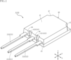
- FIG. 1 is a perspective view of a semiconductor device according to a first embodiment of the present disclosure.
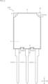
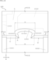
- FIG. 2 is a plan view of the semiconductor device shown in FIG.
- FIG. 3 is a plan view corresponding to FIG. 2, seen through the sealing resin.
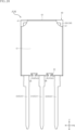
- FIG. 4 is a bottom view of the semiconductor device shown in FIG.
- FIG. 5 is a front view of the semiconductor device shown in FIG.
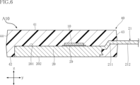
- FIG. 6 is a cross-sectional view taken along line VI-VI in FIG.
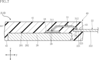
- FIG. 7 is a cross-sectional view taken along line VII-VII in FIG.
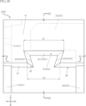
- FIG. 8 is a cross-sectional view taken along line VIII-VIII in FIG.
- FIG. 9 is a partially enlarged view of FIG.
- FIG. 10 is a partially enlarged view of FIG. FIG.
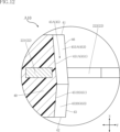
- FIG. 11 is a cross-sectional view taken along line XI-XI of FIG.
- FIG. 12 is a cross-sectional view taken along line XII-XII in FIG.
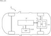
- FIG. 13 is a schematic diagram of a vehicle on which the semiconductor device shown in FIG. 1 is mounted.
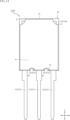
- FIG. 14 is a plan view of a semiconductor device according to a second embodiment of the present disclosure.
- FIG. 15 is a partially enlarged view of FIG.
- FIG. 16 is a cross-sectional view taken along line XVI-XVI in FIG.
- FIG. 17 is a cross-sectional view taken along line XVII-XVII in FIG.
- FIG. 18 is a plan view of a semiconductor device according to a third embodiment of the present disclosure.
- FIG. 19 is a partially enlarged view of FIG.
- FIG. 20 is a cross-sectional view taken along line XX-XX in FIG.
- FIG. 21 is a cross-sectional view taken along line XXI-XXI in FIG.
- FIG. 22 is a cross-sectional view taken along line XXII-XXII in FIG.
- FIG. 23 is a plan view of a semiconductor device according to a fourth embodiment of the present disclosure.
- FIG. 24 is a partially enlarged view of FIG.
- FIG. 25 is a cross-sectional view taken along line XXV-XXV in FIG.
- FIG. 26 is a cross-sectional view taken along line XXVI-XXVI in FIG.
- a semiconductor device A10 according to a first embodiment of the present disclosure will be described with reference to Figures 1 to 12.
- the semiconductor device A10 is used in a power conversion circuit.
- the package format of the semiconductor device A10 is a TO (Transistor Outline).
- the semiconductor device A10 includes a semiconductor element 10, a die pad 20, a first terminal 21, a second terminal 22, a third terminal 23, a conductive bonding layer 29, a conductive member 31, a wire 32, and a sealing resin 40.
- Figure 3 shows the sealing resin 40 through which the sealing resin 40 is seen.
- the see-through sealing resin 40 is indicated by an imaginary line (two-dot chain line).
- the normal direction of the mounting surface 201 of the die pad 20 described later will be referred to as the "third direction z.”
- An example of a direction perpendicular to the third direction z will be referred to as the "first direction x.”
- a direction perpendicular to both the third direction z and the first direction x will be referred to as the "second direction y.”
- the semiconductor element 10 is, for example, a MOSFET (Metal-Oxide-Semiconductor Field-Effect Transistor).
- the semiconductor element 10 may be a field effect transistor including a MISFET (Metal-Insulator-Semiconductor Field-Effect Transistor) or a bipolar transistor such as an IGBT (Insulated Gate Bipolar Transistor).
- the semiconductor element 10 is an n-channel type MOSFET with a vertical structure.
- the multiple semiconductor elements 10 include a compound semiconductor substrate.
- the composition of the compound semiconductor substrate includes silicon carbide (SiC).
- the semiconductor element 10 has a first electrode 11, a second electrode 12, and a gate electrode 13.
- the first electrode 11 is located on the side facing the mounting surface 201 of the die pad 20, which will be described later, in the third direction z.
- a current corresponding to the power before being converted by the semiconductor element 10 flows through the first electrode 11.
- the first electrode 11 corresponds to the drain electrode of the semiconductor element 10.
- the second electrode 12 is located on the opposite side to the first electrode 11 in the third direction z.
- a current corresponding to the power converted by the semiconductor element 10 flows through the second electrode 12.
- the second electrode 12 corresponds to the source electrode of the semiconductor element 10.
- the gate electrode 13 is located on the same side as the second electrode 12 in the third direction z.
- a gate voltage for driving the semiconductor element 10 is applied to the gate electrode 13.
- the area of the gate electrode 13 is smaller than the area of the second electrode 12.
- the die pad 20 is a conductive member on which the semiconductor element 10 is mounted, as shown in FIG. 3 and FIG. 6 to FIG. 8.
- the die pad 20, together with the first terminal 21, the second terminal 22, and the third terminal 23, are obtained from the same lead frame.
- the lead frame is copper (Cu) or a copper alloy. Therefore, the composition of each of the die pad 20, the first terminal 21, the second terminal 22, and the third terminal 23 includes copper.
- the die pad 20 has a mounting surface 201 and a back surface 202.
- the mounting surface 201 faces the side facing the semiconductor element 10 in the third direction z. A part of the mounting surface 201 is covered with the sealing resin 40.
- the back surface 202 faces the opposite side to the mounting surface 201 in the third direction z.
- the back surface 202 is plated with, for example, tin (Sn). The back surface 202 is exposed from the sealing resin 40.
- the conductive bonding layer 29 bonds the die pad 20 and the semiconductor element 10.
- the first electrode 11 of the semiconductor element 10 is conductively bonded to the mounting surface 201 of the die pad 20 via the conductive bonding layer 29. This allows the first electrode 11 to be electrically connected to the die pad 20.
- the conductive bonding layer 29 is, for example, solder. Alternatively, the conductive bonding layer 29 may be a sintered metal.
- the first terminal 21 includes a portion extending in the second direction y and is connected to the die pad 20. As a result, the first terminal 21 is electrically connected to the first electrode 11 of the semiconductor element 10. Therefore, the first terminal 21 corresponds to the drain terminal of the semiconductor device A10. The first terminal 21 is located on one side of the die pad 20 in the second direction y.
- the first terminal 21 has a first inner part 211 and a first outer part 212.
- the first inner part 211 is connected to the die pad 20 and is covered with the sealing resin 40. When viewed in the first direction x, the first inner part 211 is bent.
- the first outer part 212 is connected to the first inner part 211 and is exposed from the sealing resin 40.
- the first outer part 212 protrudes from the sealing resin 40 on the side opposite to the side where the die pad 20 is located in the second direction y.
- the surface of the first outer part 212 is, for example, tin-plated.
- the second terminal 22 is spaced apart from the die pad 20, as shown in Figures 3 and 7.
- the second terminal 22 extends in the second direction y.
- the second terminal 22 is electrically connected to the second electrode 12 of the semiconductor element 10. Therefore, the second terminal 22 corresponds to the source terminal of the semiconductor device A10.
- the second terminal 22 is located next to the first terminal 21 in the first direction x.
- the second terminal 22 has a second inner part 221, a second outer part 222, and a first bonding surface 223.
- the second inner part 221 is covered with the sealing resin 40.
- the second outer part 222 is connected to the second inner part 221 and is exposed from the sealing resin 40.
- the second outer part 222 protrudes from the sealing resin 40 on the side opposite to the side on which the die pad 20 is located in the second direction y.
- the surface of the second outer part 222 is plated with tin, for example.
- the first bonding surface 223 faces the same side as the mounting surface 201 of the die pad 20 in the third direction z.
- the first bonding surface 223 is included in a part of the second inner part 221.
- the first bonding surface 223 is located on the side on which the semiconductor element 10 is located in the third direction z from the mounting surface 201.
- the third terminal 23 is separated from the die pad 20.
- the third terminal 23 extends in the second direction y.
- the third terminal 23 is electrically connected to the gate electrode 13 of the semiconductor element 10. Therefore, the third terminal 23 corresponds to the gate terminal of the semiconductor device A10.
- the third terminal 23 is located on the opposite side to the second terminal 22 with respect to the first terminal 21 in the first direction x.
- the third terminal 23 has a third inner part 231, a third outer part 232, and a second bonding surface 233.
- the third inner part 231 is covered with the sealing resin 40.
- the third outer part 232 is connected to the third inner part 231 and is exposed from the sealing resin 40.
- the third outer part 232 protrudes from the sealing resin 40 on the side opposite to the side on which the die pad 20 is located in the second direction y.
- the surface of the third outer part 232 is plated with tin, for example.
- the second bonding surface 233 faces the same side as the mounting surface 201 of the die pad 20 in the third direction z.
- the second bonding surface 233 is included in a part of the third inner part 231. In the third direction z, the position of the second bonding surface 233 is the same (or approximately the same) as the position of the first bonding surface 223 of the second terminal 22.
- the first terminal 21, the second terminal 22, and the third terminal 23 are arranged along the first direction x.
- the first outer part 212 of the first terminal 21, the second outer part 222 of the second terminal 22, and the third outer part 232 of the third terminal 23 all have the same height h from the bottom surface 42 of the sealing resin 40 described below.
- the conductive member 31 is conductively bonded to the second electrode 12 of the semiconductor element 10 and the first bonding surface 223 of the second terminal 22.
- the second terminal 22 is conductive to the second electrode 12.
- the conductive member 31 contains copper or a copper alloy.
- the conductive member 31 is a metal clip. Alternatively, the conductive member 31 may be a wire.
- the conductive member 31 has a first bonding portion 311 and a second bonding portion 312.
- the first bonding portion 311 is located at one end of the conductive member 31 and is conductively bonded to the second electrode 12 via the conductive bonding layer 29.
- the second bonding portion 312 is located at the other end of the conductive member 31 and is conductively bonded to the first bonding surface 223 via the conductive bonding layer 29.
- the wire 32 is conductively bonded to the gate electrode 13 of the semiconductor element 10 and the second bonding surface 233 of the third terminal 23. This allows the third terminal 23 to be electrically connected to the gate electrode 13.
- the wire 32 contains, for example, either aluminum or gold (Au).
- the sealing resin 40 covers the semiconductor element 10, the conductive member 31, and the wires 32.
- the sealing resin 40 covers a portion of each of the die pad 20, the first terminal 21, the second terminal 22, and the third terminal 23.
- the sealing resin 40 has electrical insulation properties.
- the sealing resin 40 is made of a material that contains, for example, black epoxy resin.
- the sealing resin 40 has a top surface 41, a bottom surface 42, a first side surface 43, and a second side surface 44.
- the top surface 41 faces the same side as the mounting surface 201 of the die pad 20 in the third direction z.
- the bottom surface 42 faces the opposite side to the top surface 41 in the third direction z.
- the back surface 202 of the first portion 20A of the die pad 20 is exposed from the bottom surface 42.
- the first side surface 43 and the second side surface 44 face opposite each other in the second direction y.
- Each of the first side surface 43 and the second side surface 44 is connected to the top surface 41 and the bottom surface 42.
- Each of the first outer portion 212 of the first terminal 21, the second outer portion 222 of the second terminal 22, and the third outer portion 232 of the third terminal 23 is exposed from the first side surface 43 and protrudes from the first side surface 43 in the second direction y.
- the sealing resin 40 has two recesses 45, two openings 46, and two notches 47.
- each of the two recesses 45 is recessed from the first side surface 43.
- the semiconductor element 10 is located on the opposite side of the first side surface 43 in the second direction y with respect to the two recesses 45.
- Each of the two recesses 45 is connected to the top surface 41 and the bottom surface 42.
- the two recesses 45 include a first recess 45A and a second recess 45B.
- the first recess 45A is located between the first terminal 21 and the second terminal 22 in the first direction x.
- the second recess 45B is located between the first terminal 21 and the third terminal 23 in the first direction x.
- the two openings 46 individually define the boundaries between each of the two recesses 45 and the first side surface 43. Each of the two openings 46 is connected to the top surface 41 and the bottom surface 42.
- the dimension B1 in the first direction x of each of the two recesses 45 is greater than the dimension B2 in the first direction x of each of the two openings 46.
- the sealing resin 40 has two first surfaces 451, two second surfaces 452, and two third surfaces 453 that individually define each of the two recesses 45.
- first surface 451, the second surface 452, and the third surface 453 that define the first recess 45A of the two recesses 45 will be representatively explained.
- the first surface 451 is located between the first side surface 43 and the semiconductor element 10.
- the second inner portion 221 of the second terminal 22 overlaps the first surface 451 when viewed in the second direction y.
- the second surface 452 is located between the first side surface 43 and the first surface 451, and defines one of the two openings 46.
- the third surface 453 faces the second surface 452 in the first direction x, and defines one of the two openings 46. In a direction perpendicular to the third direction z, each of the second surface 452 and the third surface 453 includes a region that faces a direction different from the direction in which the first surface 451 faces.
- the dimension of the first surface 451 in the first direction x is greater than the dimension B2 in the first direction x of each of the two openings 46.
- each of the second surface 452 and the third surface 453 is inclined with respect to the first direction x.
- the distance between the second surface 452 and the third surface 453 in the first direction x increases from one of the two openings 46 toward the first surface 451.
- the first surface 451 includes a first region 451A and a second region 451B.
- the second region 451B is located on the opposite side of the top surface 41 in the third direction z with the first region 451A as a reference.
- the first region 451A is connected to the top surface 41.
- the second region 451B is connected to each of the bottom surface 42 and the first region 451A.
- the first region 451A is inclined with respect to the third direction z in a direction approaching the first side surface 43 from the top surface 41 toward the bottom surface 42.
- the second region 451B is inclined with respect to the third direction z in a direction approaching the first side surface 43 from the bottom surface 42 toward the top surface 41.
- the second surface 452 includes a third region 452A and a fourth region 452B.
- the fourth region 452B is located on the opposite side of the top surface 41 in the third direction z with the third region 452A as a reference.
- the third region 452A is connected to the top surface 41.
- the fourth region 452B is connected to both the bottom surface 42 and the third region 452A.
- the third region 452A is inclined with respect to the third direction z in a direction approaching the third surface 453 from the top surface 41 toward the bottom surface 42.
- the fourth region 452B is inclined with respect to the third direction z in a direction approaching the third surface 453 from the bottom surface 42 toward the top surface 41.
- the third surface 453 includes a fifth region 453A and a sixth region 453B.
- the sixth region 453B is located on the opposite side of the top surface 41 with respect to the fifth region 453A in the third direction z.
- the fifth region 453A is connected to the top surface 41.
- the sixth region 453B is connected to both the bottom surface 42 and the fifth region 453A.
- the fifth region 453A is inclined with respect to the third direction z in a direction approaching the second surface 452 from the top surface 41 toward the bottom surface 42.
- the sixth region 453B is inclined with respect to the third direction z in a direction approaching the second surface 452 from the bottom surface 42 toward the top surface 41.
- each of the second region 451B, the fourth region 452B, and the sixth region 453B is separated from the second inner portion 221 of the second terminal 22 in the third direction z.
- the two cutouts 47 are spaced apart from each other in the first direction x. As shown in FIG. 2 and FIG. 8, each of the two cutouts 47 is recessed from each of the top surface 41 and the second side surface 44. The mounting surface 201 of the die pad 20 is exposed from each of the two cutouts 47.
- the vehicle B is, for example, an electric vehicle (EV).
- EV electric vehicle
- vehicle B is equipped with an on-board charger 81, a storage battery 82, and a drive system 83.
- Power is supplied to the on-board charger 81 wirelessly from a power supply facility (not shown) installed outdoors. Alternatively, power may be supplied from the power supply facility to the on-board charger 81 via a wired connection.
- a step-up DC-DC converter is configured in the on-board charger 81.
- Semiconductor device A10 forms part of the converter.
- the components of the on-board charger 81 include semiconductor device A10.
- the voltage of the power supplied to the on-board charger 81 is stepped up by the converter and then supplied to the storage battery 82.
- the stepped-up voltage is, for example, 600V.
- the drive system 83 drives the vehicle B.
- the drive system 83 has an inverter 831 and a drive source 832.
- the power stored in the storage battery 82 is supplied to the inverter 831.
- the power supplied from the storage battery 82 to the inverter 831 is DC power.
- a step-up DC-DC converter may be further provided between the storage battery 82 and the inverter 831.
- the inverter 831 converts DC power into AC power.
- the inverter 831 is conductive to the drive source 832.
- the drive source 832 has an AC motor and a transmission. When the AC power converted by the inverter 831 is supplied to the drive source 832, the AC motor rotates and the rotation is transmitted to the transmission.
- the transmission appropriately reduces the rotation speed transmitted from the AC motor and then rotates the drive shaft of the vehicle B. This drives the vehicle B.
- the inverter 831 is capable of freely changing the rotation speed of the AC motor based on information such as the amount of fluctuation in the accelerator pedal.
- the semiconductor device A10 includes a first terminal 21, a second terminal 22, a semiconductor element 10, and a sealing resin 40.
- the sealing resin 40 has a first side 43 on which the first terminal 21 and the second terminal 22 are exposed.
- the sealing resin 40 has a recess 45 recessed from the first side 43 and an opening 46 forming a boundary between the first side 43 and the recess 45.
- the recess 45 is located between the first terminal 21 and the second terminal 22 in the first direction x.
- the dimension B1 of the recess 45 in the first direction x is larger than the dimension B2 of the opening 46 in the first direction x.
- the sealing resin 40 has a top surface 41 and a bottom surface 42.
- the recesses 45 and the openings 46 are each connected to the top surface 41 and the bottom surface 42. This configuration makes it possible to make the distribution of the creepage distance along the surface of the sealing resin 40 from the first terminal 21 to the second terminal 22 more uniform.
- the sealing resin 40 has a first surface 451, a second surface 452, and a third surface 453, each of which defines a recess 45.
- each of the second surface 452 and the third surface 453 includes an area that faces in a direction different from the direction in which the first surface 451 faces.
- the dimension of the first surface 451 in the first direction x is larger than the dimension B2 of the opening 46 in the first direction x.
- the second surface 452 and the third surface 453 are each inclined with respect to the first direction x.
- the distance in the first direction x between the second surface 452 and the third surface 453 increases from the opening 46 toward the first surface 451. This configuration makes it possible to minimize the number of surfaces that define the recess 45 while increasing the creepage distance along the surface of the sealing resin 40 from the first terminal 21 to the second terminal 22.
- the second inner portion 221 of the second terminal 22 overlaps the first surface 451.
- This configuration makes it possible to miniaturize the semiconductor device A10 while further increasing the area of the first bonding surface 223 of the second terminal 22 to which the conductive member 31 is conductively bonded.
- the first surface 451 includes a first region 451A and a second region 451B.
- the first region 451A is inclined with respect to the third direction z in a direction approaching the first side surface 43 from the top surface 41 toward the bottom surface 42.
- the second region 451B is inclined with respect to the third direction z in a direction approaching the first side surface 43 from the bottom surface 42 toward the top surface 41. This configuration can prevent damage to the first surface 451 that occurs when the mold used to form the sealing resin 40 is removed.
- the second surface 452 includes a third region 452A and a fourth region 452B.
- the third region 452A is inclined with respect to the third direction z in a direction approaching the third surface 453 from the top surface 41 toward the bottom surface 42.
- the fourth region 452B is inclined with respect to the third direction z in a direction approaching the first side surface 43 from the bottom surface 42 toward the top surface 41. This configuration can prevent damage to the second surface 452 that occurs when the mold used to form the sealing resin 40 is removed.
- the semiconductor device A10 further includes a die pad 20 to which the semiconductor element 10 is conductively bonded.
- the first terminal 21 is connected to the die pad 20.
- the die pad 20 is exposed from the bottom surface 42. With this configuration, the die pad 20 can be used as a conductive path while the heat generated by the semiconductor element 10 can be more efficiently released to the outside.
- a semiconductor device A20 according to a second embodiment of the present disclosure will be described with reference to Figures 14 to 17.
- elements that are the same as or similar to those of the semiconductor device A10 described above are given the same reference numerals, and duplicated descriptions will be omitted.
- the boundary between the first surface 451 and the third surface 453 of the sealing resin 40 is indicated by a two-dot chain line.
- semiconductor device A20 the configuration of the two recesses 45 provided in the sealing resin 40 differs from that of semiconductor device A10.
- the first surface 451 that defines each of the two recesses 45 includes a curved area.
- the entire first surface 451 forms a curved surface that is concave on the side where the semiconductor element 10 is located in the second direction y.
- the dimension B1 in the first direction x of each of the two recesses 45 is greater than the dimension B2 in the first direction x of each of the two openings 46.
- the semiconductor device A20 includes a first terminal 21, a second terminal 22, a semiconductor element 10, and a sealing resin 40.
- the sealing resin 40 has a first side 43 on which the first terminal 21 and the second terminal 22 are exposed.
- the sealing resin 40 includes a recess 45 recessed from the first side 43 and an opening 46 forming a boundary between the first side 43 and the recess 45.
- the recess 45 is located between the first terminal 21 and the second terminal 22 in the first direction x.
- the dimension B1 of the recess 45 in the first direction x is larger than the dimension B2 of the opening 46 in the first direction x. Therefore, according to this configuration, the semiconductor device A20 can also be made smaller while improving the dielectric strength.
- the semiconductor device A20 has a configuration common to the semiconductor device A10, and thus has the same effect as the semiconductor device A10.
- a semiconductor device A30 according to a third embodiment of the present disclosure will be described with reference to Fig. 18 to Fig. 22.
- elements that are the same as or similar to those of the semiconductor device A10 described above are given the same reference numerals, and duplicated descriptions will be omitted.
- semiconductor device A30 the configuration of the two recesses 45 provided in the sealing resin 40 differs from that of semiconductor device A10.
- the sealing resin 40 has two fourth surfaces 454 and two fifth surfaces 455 that individually define each of the two recesses 45.
- the fourth surface 454 and the fifth surface 455 that define the first recess 45A of the two recesses 45 will be representatively explained.
- the fourth surface 454 is located between the first surface 451 and the second and third surfaces 452 and 453.
- the fourth surface 454 is located on the opposite side of the third surface 453 with respect to the second surface 452 in the first direction x.
- the fifth surface 455 faces the fourth surface 454 in the first direction x.
- the fifth surface 455 is located on the opposite side of the second surface 452 with respect to the third surface 453 in the first direction x.
- the dimension B1 in the first direction x of each of the two recesses 45 is greater than the dimension B2 in the first direction x of each of the two openings 46.
- the distance in the first direction x between the fourth surface 454 and the fifth surface 455 is greater than the dimension B2 in the first direction x of either of the two openings 46.
- the distance in the first direction x between the fourth surface 454 and the fifth surface 455 is greater than the distance in the first direction x between the second surface 452 and the third surface 453.
- the maximum distance in the first direction x between the fourth surface 454 and the fifth surface 455 is equal to the dimension in the first direction x of the first surface 451.
- the fourth surface 454 includes a seventh region 454A and an eighth region 454B.
- the eighth region 454B is located on the opposite side of the top surface 41 with respect to the seventh region 454A in the third direction z.
- the seventh region 454A is connected to the top surface 41.
- the eighth region 454B is connected to both the bottom surface 42 and the seventh region 454A.
- the seventh region 454A is inclined with respect to the third direction z in a direction approaching the fifth surface 455 from the top surface 41 toward the bottom surface 42.
- the eighth region 454B is inclined with respect to the third direction z in a direction approaching the fifth surface 455 from the bottom surface 42 toward the top surface 41.
- the fifth surface 455 includes a ninth region 455A and a tenth region 455B.
- the tenth region 455B is located on the opposite side of the top surface 41 with respect to the ninth region 455A in the third direction z.
- the ninth region 455A is connected to the top surface 41.
- the tenth region 455B is connected to both the bottom surface 42 and the ninth region 455A.
- the ninth region 455A is inclined with respect to the third direction z in a direction approaching the fourth surface 454 from the top surface 41 toward the bottom surface 42.
- the tenth region 455B is inclined with respect to the third direction z in a direction approaching the fourth surface 454 from the bottom surface 42 toward the top surface 41.
- the semiconductor device A30 includes a first terminal 21, a second terminal 22, a semiconductor element 10, and a sealing resin 40.
- the sealing resin 40 has a first side 43 on which the first terminal 21 and the second terminal 22 are exposed.
- the sealing resin 40 includes a recess 45 recessed from the first side 43 and an opening 46 forming a boundary between the first side 43 and the recess 45.
- the recess 45 is located between the first terminal 21 and the second terminal 22 in the first direction x.
- the dimension B1 of the recess 45 in the first direction x is larger than the dimension B2 of the opening 46 in the first direction x. Therefore, according to this configuration, the semiconductor device A30 can also be made smaller while improving the dielectric strength. Furthermore, the semiconductor device A30 has a configuration common to the semiconductor device A10, thereby achieving the same effects as the semiconductor device A10.
- the sealing resin 40 has a fourth surface 454 and a fifth surface 455, each of which defines a recess 45.
- the distance in the first direction x between the fourth surface 454 and the fifth surface 455 is greater than the dimension B2 in the first direction x of the opening 46.
- the distance in the first direction x between the fourth surface 454 and the fifth surface 455 is greater than the distance in the first direction x between the second surface 452 and the third surface 453. This configuration makes it possible to further increase the creepage distance along the surface of the sealing resin 40 from the first terminal 21 to the second terminal 22.
- a semiconductor device A40 according to a fourth embodiment of the present disclosure will be described with reference to Fig. 23 to Fig. 26.
- elements that are the same as or similar to those of the semiconductor device A10 described above are given the same reference numerals, and duplicated descriptions will be omitted.
- the configuration of the two recesses 45 provided in the sealing resin 40 differs from that of semiconductor device A30.
- the sealing resin 40 has two sixth surfaces 456 and two seventh surfaces 457 that individually define each of the two recesses 45.
- the sixth surface 456 and the seventh surface 457 that define the first recess 45A of the two recesses 45 will be representatively explained.
- the sixth surface 456 is located between the first surface 451 and the fourth and fifth surfaces 454 and 455.
- the seventh surface 457 faces the sixth surface 456 in the first direction x.
- Each of the sixth surface 456 and the seventh surface 457 is located between the fourth surface 454 and the fifth surface 455 in the first direction x.
- the dimension B1 in the first direction x of each of the two recesses 45 is greater than the dimension B2 in the first direction x of each of the two openings 46.
- the maximum distance in the first direction x between the fourth surface 454 and the fifth surface 455 is greater than the dimension in the first direction x of the first surface 451.
- the maximum distance in the first direction x between the sixth surface 456 and the seventh surface 457 is equal to the dimension in the first direction x of the first surface 451.
- the sixth surface 456 includes an eleventh region 456A and a twelfth region 456B.
- the twelfth region 456B is located on the opposite side of the top surface 41 in the third direction z with the eleventh region 456A as a reference.
- the eleventh region 456A is connected to the top surface 41.
- the twelfth region 456B is connected to both the bottom surface 42 and the eleventh region 456A.
- the eleventh region 456A is inclined with respect to the third direction z in a direction approaching the seventh surface 457 from the top surface 41 toward the bottom surface 42.
- the twelfth region 456B is inclined with respect to the third direction z in a direction approaching the seventh surface 457 from the bottom surface 42 toward the top surface 41.
- the seventh surface 457 includes a thirteenth region 457A and a fourteenth region 457B.
- the fourteenth region 457B is located on the opposite side of the top surface 41 in the third direction z with the thirteenth region 457A as a reference.
- the thirteenth region 457A is connected to the top surface 41.
- the fourteenth region 457B is connected to both the bottom surface 42 and the thirteenth region 457A.
- the thirteenth region 457A is inclined with respect to the third direction z in a direction approaching the sixth surface 456 from the top surface 41 toward the bottom surface 42.
- the fourteenth region 457B is inclined with respect to the third direction z in a direction approaching the sixth surface 456 from the bottom surface 42 toward the top surface 41.
- the semiconductor device A40 includes a first terminal 21, a second terminal 22, a semiconductor element 10, and a sealing resin 40.
- the sealing resin 40 has a first side 43 on which the first terminal 21 and the second terminal 22 are exposed.
- the sealing resin 40 includes a recess 45 recessed from the first side 43 and an opening 46 forming a boundary between the first side 43 and the recess 45.
- the recess 45 is located between the first terminal 21 and the second terminal 22 in the first direction x.
- the dimension B1 of the recess 45 in the first direction x is larger than the dimension B2 of the opening 46 in the first direction x. Therefore, according to this configuration, the semiconductor device A40 can also be made smaller while improving the dielectric strength.
- the semiconductor device A40 has a configuration common to the semiconductor device A10, and thus has the same effect as the semiconductor device A10.
- the maximum distance in the first direction x between the fourth surface 454 and the fifth surface 455 is greater than the dimension in the first direction x of the first surface 451.
- the present disclosure is not limited to the above-described embodiment.
- the specific configuration of each part of the present disclosure can be freely designed in various ways.
- the technology disclosed herein can also be applied to semiconductor devices with a DIP (Dual Inline Package) package format, for example.
- Appendix 1 A first terminal; a second terminal located adjacent to the first terminal in a first direction; a semiconductor element electrically connected to each of the first terminal and the second terminal; a sealing resin covering a portion of each of the first terminal and the second terminal and the semiconductor element, the sealing resin has a first side surface facing a second direction perpendicular to the first direction, each of the first terminal and the second terminal is exposed from the first side surface; the sealing resin is provided with a recess that is located between the first terminal and the second terminal in the first direction and recessed from the first side surface, and an opening that forms a boundary between the first side surface and the recess, a dimension of the recess in the first direction being larger than a dimension of the opening in the first direction.
- the sealing resin has a top surface and a bottom surface facing opposite sides in a third direction perpendicular to the first direction and the second direction, 2.
- Appendix 3. the semiconductor element is located on an opposite side to the first side surface with respect to the recess in the second direction, the sealing resin has a first surface, a second surface, and a third surface each defining the recess; the first surface is located between the first side surface and the semiconductor element, the second surface is located between the first side surface and the first surface and defines the opening; the third surface faces the second surface in the first direction and defines the opening, 3.
- the second surface and the third surface each include a region facing in a direction different from a direction in which the first surface faces.
- Appendix 4. The semiconductor device according to claim 3, wherein a dimension of the first surface in the first direction is larger than a dimension of the opening in the first direction.
- Appendix 5. each of the second surface and the third surface is inclined with respect to the first direction; 5.
- the second terminal has an inner portion covered with the sealing resin, 6.
- the first surface includes a first region and a second region located on an opposite side of the top surface with respect to the first region in the third direction, the first region is inclined with respect to the third direction in a direction approaching the first side surface from the top surface toward the bottom surface, 7.
- Appendix 8. the second surface includes a third region and a fourth region located on an opposite side to the top surface with respect to the first region in the third direction, the third region is inclined with respect to the third direction in a direction approaching the third surface from the top surface toward the bottom surface, 8.
- the sealing resin has a fourth surface and a fifth surface each defining the recess; the fourth surface is located between the first surface, the second surface, and the third surface; the fifth surface faces the fifth surface in the first direction, 4.
- a distance between the fourth surface and the fifth surface in the first direction is greater than a dimension of the opening in the first direction.
- Appendix 10. 10. The semiconductor device according to claim 9, wherein a distance in the first direction between the fourth surface and the fifth surface is greater than a distance in the first direction between the second surface and the third surface. Appendix 11. 11.
- the semiconductor element further includes a die pad to which the die pad is conductively bonded.
- Appendix 17. A semiconductor device according to claim 13; An on-board charger, A storage battery that is in electrical communication with the on-board charger; a drive system connected to the storage battery; A vehicle, wherein components of the vehicle-mounted charger include the semiconductor device.
Landscapes
- Structures Or Materials For Encapsulating Or Coating Semiconductor Devices Or Solid State Devices (AREA)
Priority Applications (1)
| Application Number | Priority Date | Filing Date | Title |
|---|---|---|---|
| JP2025510142A JPWO2024203066A1 (https=) | 2023-03-28 | 2024-03-06 |
Applications Claiming Priority (2)
| Application Number | Priority Date | Filing Date | Title |
|---|---|---|---|
| JP2023050923 | 2023-03-28 | ||
| JP2023-050923 | 2023-03-28 |
Publications (1)
| Publication Number | Publication Date |
|---|---|
| WO2024203066A1 true WO2024203066A1 (ja) | 2024-10-03 |
Family
ID=92905578
Family Applications (1)
| Application Number | Title | Priority Date | Filing Date |
|---|---|---|---|
| PCT/JP2024/008488 Ceased WO2024203066A1 (ja) | 2023-03-28 | 2024-03-06 | 半導体装置および車両 |
Country Status (2)
| Country | Link |
|---|---|
| JP (1) | JPWO2024203066A1 (https=) |
| WO (1) | WO2024203066A1 (https=) |
Citations (3)
| Publication number | Priority date | Publication date | Assignee | Title |
|---|---|---|---|---|
| JPS59115653U (ja) * | 1983-01-25 | 1984-08-04 | サンケン電気株式会社 | 絶縁物封止半導体装置 |
| US7199461B2 (en) * | 2003-01-21 | 2007-04-03 | Fairchild Korea Semiconductor, Ltd | Semiconductor package suitable for high voltage applications |
| US20160365296A1 (en) * | 2015-06-09 | 2016-12-15 | Infineon Technologies Ag | Electronic Devices with Increased Creepage Distances |
-
2024
- 2024-03-06 JP JP2025510142A patent/JPWO2024203066A1/ja active Pending
- 2024-03-06 WO PCT/JP2024/008488 patent/WO2024203066A1/ja not_active Ceased
Patent Citations (3)
| Publication number | Priority date | Publication date | Assignee | Title |
|---|---|---|---|---|
| JPS59115653U (ja) * | 1983-01-25 | 1984-08-04 | サンケン電気株式会社 | 絶縁物封止半導体装置 |
| US7199461B2 (en) * | 2003-01-21 | 2007-04-03 | Fairchild Korea Semiconductor, Ltd | Semiconductor package suitable for high voltage applications |
| US20160365296A1 (en) * | 2015-06-09 | 2016-12-15 | Infineon Technologies Ag | Electronic Devices with Increased Creepage Distances |
Also Published As
| Publication number | Publication date |
|---|---|
| JPWO2024203066A1 (https=) | 2024-10-03 |
Similar Documents
| Publication | Publication Date | Title |
|---|---|---|
| US6307272B1 (en) | Semiconductor device and method for manufacturing the same | |
| US8581376B2 (en) | Stacked dual chip package and method of fabrication | |
| US11710709B2 (en) | Terminal member made of plurality of metal layers between two heat sinks | |
| US8345458B2 (en) | Semiconductor device | |
| CN101378053B (zh) | 高、低压侧n沟道金属氧化物半导体场效应晶体管组合封装 | |
| US7615854B2 (en) | Semiconductor package that includes stacked semiconductor die | |
| US20220301965A1 (en) | Semiconductor device | |
| EP3686925B1 (en) | Semiconductor device and power conversion device provided with same | |
| US20250374649A1 (en) | Semiconductor device and vehicle | |
| US20250372511A1 (en) | Semiconductor device and vehicle | |
| US20220301966A1 (en) | Semiconductor device | |
| WO2024203066A1 (ja) | 半導体装置および車両 | |
| WO2025158862A1 (ja) | 半導体装置および車両 | |
| US20260090403A1 (en) | Semiconductor device and vehicle | |
| WO2026079464A1 (ja) | 半導体装置および車両 | |
| WO2024095788A1 (ja) | 半導体装置 | |
| WO2021181678A1 (ja) | 半導体装置および電力変換装置 | |
| US20260053054A1 (en) | Semiconductor device, method for manufacturing semiconductor device, and vehicle | |
| JP5758816B2 (ja) | パワー半導体装置 | |
| JP2025179918A (ja) | 半導体装置および車両 | |
| WO2024225036A1 (ja) | 半導体装置および車両 | |
| WO2024209899A1 (ja) | 半導体装置および車両 | |
| WO2024190426A1 (ja) | 半導体装置および車両 | |
| WO2024228322A1 (ja) | 半導体装置 | |
| JP2025098863A (ja) | 半導体装置および車両 |
Legal Events
| Date | Code | Title | Description |
|---|---|---|---|
| 121 | Ep: the epo has been informed by wipo that ep was designated in this application |
Ref document number: 24779201 Country of ref document: EP Kind code of ref document: A1 |
|
| ENP | Entry into the national phase |
Ref document number: 2025510142 Country of ref document: JP Kind code of ref document: A |
|
| WWE | Wipo information: entry into national phase |
Ref document number: 2025510142 Country of ref document: JP |
|
| NENP | Non-entry into the national phase |
Ref country code: DE |
|
| 122 | Ep: pct application non-entry in european phase |
Ref document number: 24779201 Country of ref document: EP Kind code of ref document: A1 |