WO2024202402A1 - 積層セラミック電子部品 - Google Patents
積層セラミック電子部品 Download PDFInfo
- Publication number
- WO2024202402A1 WO2024202402A1 PCT/JP2024/000953 JP2024000953W WO2024202402A1 WO 2024202402 A1 WO2024202402 A1 WO 2024202402A1 JP 2024000953 W JP2024000953 W JP 2024000953W WO 2024202402 A1 WO2024202402 A1 WO 2024202402A1
- Authority
- WO
- WIPO (PCT)
- Prior art keywords
- spacer
- capacitor body
- protective material
- multilayer ceramic
- region
- Prior art date
- Legal status (The legal status is an assumption and is not a legal conclusion. Google has not performed a legal analysis and makes no representation as to the accuracy of the status listed.)
- Ceased
Links
Images


Classifications
-
- H—ELECTRICITY
- H01—ELECTRIC ELEMENTS
- H01G—CAPACITORS; CAPACITORS, RECTIFIERS, DETECTORS, SWITCHING DEVICES, LIGHT-SENSITIVE OR TEMPERATURE-SENSITIVE DEVICES OF THE ELECTROLYTIC TYPE
- H01G2/00—Details of capacitors not covered by a single one of groups H01G4/00-H01G11/00
- H01G2/10—Housing; Encapsulation
-
- H—ELECTRICITY
- H01—ELECTRIC ELEMENTS
- H01G—CAPACITORS; CAPACITORS, RECTIFIERS, DETECTORS, SWITCHING DEVICES, LIGHT-SENSITIVE OR TEMPERATURE-SENSITIVE DEVICES OF THE ELECTROLYTIC TYPE
- H01G4/00—Fixed capacitors; Processes of their manufacture
- H01G4/30—Stacked capacitors
-
- H—ELECTRICITY
- H01—ELECTRIC ELEMENTS
- H01C—RESISTORS
- H01C7/00—Non-adjustable resistors formed as one or more layers or coatings; Non-adjustable resistors made from powdered conducting material or powdered semi-conducting material with or without insulating material
- H01C7/02—Non-adjustable resistors formed as one or more layers or coatings; Non-adjustable resistors made from powdered conducting material or powdered semi-conducting material with or without insulating material having positive temperature coefficient
-
- H—ELECTRICITY
- H01—ELECTRIC ELEMENTS
- H01C—RESISTORS
- H01C7/00—Non-adjustable resistors formed as one or more layers or coatings; Non-adjustable resistors made from powdered conducting material or powdered semi-conducting material with or without insulating material
- H01C7/04—Non-adjustable resistors formed as one or more layers or coatings; Non-adjustable resistors made from powdered conducting material or powdered semi-conducting material with or without insulating material having negative temperature coefficient
-
- H—ELECTRICITY
- H01—ELECTRIC ELEMENTS
- H01C—RESISTORS
- H01C7/00—Non-adjustable resistors formed as one or more layers or coatings; Non-adjustable resistors made from powdered conducting material or powdered semi-conducting material with or without insulating material
- H01C7/10—Non-adjustable resistors formed as one or more layers or coatings; Non-adjustable resistors made from powdered conducting material or powdered semi-conducting material with or without insulating material voltage responsive, i.e. varistors
-
- H—ELECTRICITY
- H01—ELECTRIC ELEMENTS
- H01G—CAPACITORS; CAPACITORS, RECTIFIERS, DETECTORS, SWITCHING DEVICES, LIGHT-SENSITIVE OR TEMPERATURE-SENSITIVE DEVICES OF THE ELECTROLYTIC TYPE
- H01G2/00—Details of capacitors not covered by a single one of groups H01G4/00-H01G11/00
- H01G2/02—Mountings
-
- H—ELECTRICITY
- H01—ELECTRIC ELEMENTS
- H01G—CAPACITORS; CAPACITORS, RECTIFIERS, DETECTORS, SWITCHING DEVICES, LIGHT-SENSITIVE OR TEMPERATURE-SENSITIVE DEVICES OF THE ELECTROLYTIC TYPE
- H01G2/00—Details of capacitors not covered by a single one of groups H01G4/00-H01G11/00
- H01G2/02—Mountings
- H01G2/06—Mountings specially adapted for mounting on a printed-circuit support
- H01G2/065—Mountings specially adapted for mounting on a printed-circuit support for surface mounting, e.g. chip capacitors
-
- H—ELECTRICITY
- H01—ELECTRIC ELEMENTS
- H01G—CAPACITORS; CAPACITORS, RECTIFIERS, DETECTORS, SWITCHING DEVICES, LIGHT-SENSITIVE OR TEMPERATURE-SENSITIVE DEVICES OF THE ELECTROLYTIC TYPE
- H01G4/00—Fixed capacitors; Processes of their manufacture
- H01G4/002—Details
- H01G4/005—Electrodes
- H01G4/012—Form of non-self-supporting electrodes
-
- H—ELECTRICITY
- H01—ELECTRIC ELEMENTS
- H01G—CAPACITORS; CAPACITORS, RECTIFIERS, DETECTORS, SWITCHING DEVICES, LIGHT-SENSITIVE OR TEMPERATURE-SENSITIVE DEVICES OF THE ELECTROLYTIC TYPE
- H01G4/00—Fixed capacitors; Processes of their manufacture
- H01G4/002—Details
- H01G4/018—Dielectrics
- H01G4/06—Solid dielectrics
- H01G4/08—Inorganic dielectrics
- H01G4/12—Ceramic dielectrics
-
- H—ELECTRICITY
- H01—ELECTRIC ELEMENTS
- H01G—CAPACITORS; CAPACITORS, RECTIFIERS, DETECTORS, SWITCHING DEVICES, LIGHT-SENSITIVE OR TEMPERATURE-SENSITIVE DEVICES OF THE ELECTROLYTIC TYPE
- H01G4/00—Fixed capacitors; Processes of their manufacture
- H01G4/002—Details
- H01G4/224—Housing; Encapsulation
-
- H—ELECTRICITY
- H01—ELECTRIC ELEMENTS
- H01G—CAPACITORS; CAPACITORS, RECTIFIERS, DETECTORS, SWITCHING DEVICES, LIGHT-SENSITIVE OR TEMPERATURE-SENSITIVE DEVICES OF THE ELECTROLYTIC TYPE
- H01G4/00—Fixed capacitors; Processes of their manufacture
- H01G4/002—Details
- H01G4/228—Terminals
- H01G4/232—Terminals electrically connecting two or more layers of a stacked or rolled capacitor
-
- H—ELECTRICITY
- H01—ELECTRIC ELEMENTS
- H01G—CAPACITORS; CAPACITORS, RECTIFIERS, DETECTORS, SWITCHING DEVICES, LIGHT-SENSITIVE OR TEMPERATURE-SENSITIVE DEVICES OF THE ELECTROLYTIC TYPE
- H01G4/00—Fixed capacitors; Processes of their manufacture
- H01G4/002—Details
- H01G4/228—Terminals
- H01G4/248—Terminals the terminals embracing or surrounding the capacitive element, e.g. caps
Definitions
- the present invention relates to multilayer ceramic electronic components such as multilayer ceramic capacitors.
- Multilayer ceramic electronic components such as multilayer ceramic capacitors are widely used in mobile terminal devices such as mobile phones and various electronic devices such as personal computers.
- a multilayer ceramic capacitor comprises a rectangular parallelepiped laminate in which dielectric layers and internal electrode layers are alternately laminated, and external electrodes formed on both opposing ends of the laminate.
- a multilayer ceramic capacitor has an inner layer in which dielectric layers and internal electrodes are alternately stacked. Dielectric layers are then placed on the top and bottom of the inner layer as outer layers to form a rectangular parallelepiped laminate, and external electrodes are provided on both longitudinal end faces of the laminate to form the capacitor body.
- a multilayer ceramic capacitor that includes a spacer formed on the side of the capacitor body that is mounted on the board so as to cover part of the external electrode.
- the spacer may peel off, and the durability of the capacitor when mounted is insufficient.
- the objective of the present invention is to provide a multilayer ceramic capacitor that has a high adhesion between the capacitor body and the spacer and has excellent durability when mounted.
- the present invention provides a capacitor body including a laminate in which dielectric layers and internal electrode layers are alternately laminated, the laminate having two main surfaces facing each other in a lamination direction, two end faces facing each other in a length direction intersecting the lamination direction, and two side surfaces facing each other in a width direction intersecting the lamination direction and the length direction, and two external electrodes disposed on each of the two end faces, connected to the internal electrode layers, and extending to the two main surfaces to cover parts of the main surfaces and to the two side surfaces to cover parts of the side surfaces;
- the present invention provides a multilayer ceramic electronic component that includes two spacers that are disposed on one end face side and the other end face side, respectively, on the main surface side or one side face side, sandwiching the external electrode that covers the part of the main surface or the part of the side face between them, each of the spacers being longer in the length direction than the external electrode that covers the one main surface, containing a metal component and a protective material, and when divided in two in the length
- the present invention provides a multilayer ceramic capacitor that has a high adhesion between the capacitor body and the spacer and has excellent durability when mounted.
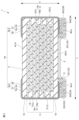
- FIG. 1 is a schematic perspective view of a multilayer ceramic capacitor 1.
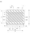
- FIG. 2 is a cross-sectional view of the multilayer ceramic capacitor 1 taken along line II-II in FIG. 2 is a cross-sectional view of the multilayer ceramic capacitor 1 taken along line III-III in FIG.
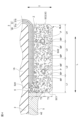
- FIG. 3 is an enlarged view of a spacer 4 portion in the cross-sectional view of the multilayer ceramic capacitor 1 in FIG. 2 .
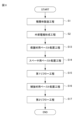
- 2 is a flowchart illustrating a method for manufacturing the multilayer ceramic capacitor 1.
- 3A to 3C are diagrams illustrating a laminate manufacturing step S1 and an external electrode forming step S2.
- 13A and 13B are diagrams illustrating a protective material and reinforcing material paste arranging step S3, a spacer paste arranging step S4, and a reflow step S5.
- 13 is a flowchart showing a process for forming a protective material 6 and a reinforcing material in a modified example.
- 13A to 13C are diagrams illustrating a protective material 6 and a reinforcing material forming step in a modified example.
- a multilayer ceramic capacitor 1 will be described as an embodiment of a multilayer ceramic electronic component of the present invention, but the present invention is not limited thereto.
- the drawings may be drawn in a schematic and simplified manner in order to explain the contents of the invention, and the dimensional ratios of the depicted components or between the components may not match those dimensional ratios described in the specification.
- components described in the specification may be omitted in the drawings, or may be drawn with the number of components omitted.
- FIG. 1 is a schematic perspective view of a multilayer ceramic capacitor 1 according to an embodiment.
- FIG. 2 is a cross-sectional view of the multilayer ceramic capacitor 1 according to an embodiment taken along line II-II in FIG. 1.
- FIG. 3 is a cross-sectional view of the multilayer ceramic capacitor 1 according to an embodiment taken along line III-III in FIG. 1.
- the multilayer ceramic capacitor 1 is substantially rectangular and includes a capacitor body 1A including a laminate 2 and a pair of external electrodes 3 provided at both ends of the laminate 2, a spacer 4 including a protective material 6 attached to the capacitor body 1A, and a reinforcing material 5 disposed between the two spacers 4.
- the laminate 2 also includes an inner layer 11 in which a dielectric layer 14 and an internal electrode layer 15 are laminated.
- the terms used to indicate the orientation of the multilayer ceramic capacitor 1 are the length direction L, which is the direction in which the pair of external electrodes 3 are provided in the multilayer ceramic capacitor 1.
- the direction in which the dielectric layers 14 and the internal electrode layers 15 are stacked is the stacking direction T.
- the direction that intersects both the length direction L and the stacking direction T is the width direction W. Note that in this embodiment, the width direction W is perpendicular to both the length direction L and the stacking direction T.
- Outer surface of laminate 2 Among the six outer surfaces of the laminate 2, a pair of outer surfaces facing each other in the stacking direction T is referred to as a first main surface A1 and a second main surface A2, a pair of outer surfaces facing each other in the width direction W is referred to as a first side surface B1 and a second side surface B2, and a pair of outer surfaces facing each other in the length direction L is referred to as a first end surface C1 and a second end surface C2.
- first main surface A1 and the second main surface A2 When it is not necessary to distinguish between the first main surface A1 and the second main surface A2, they will be collectively referred to as a main surface A, when it is not necessary to distinguish between the first side surface B1 and the second side surface B2, they will be collectively referred to as a side surface B, and when it is not necessary to distinguish between the first end surface C1 and the second end surface C2, they will be collectively referred to as an end surface C.
- the laminate 2 preferably has rounded ridges R1, including the corners.
- the ridges R1 are the intersections of two surfaces of the laminate 2, i.e., the main surface A and the side surface B, the main surface A and the end surface C, or the side surface B and the end surface C.
- the laminate 2 comprises an inner layer portion 11 that forms a capacitance, an outer layer portion 12 that is arranged to sandwich the inner layer portion 11 in the stacking direction T, and a side gap portion 16 that is arranged to sandwich the inner layer portion 11 and the outer layer portion 12 in the width direction W.
- the inner layer portion 11 includes dielectric layers 14 and internal electrode layers 15 alternately stacked along a stacking direction T.
- the dielectric layer 14 is made of a ceramic material, such as a dielectric ceramic containing BaTiO3 as a main component.
- the internal electrode layer 15 includes a plurality of first internal electrode layers 15a and a plurality of second internal electrode layers 15b.
- the first internal electrode layers 15a and the second internal electrode layers 15b are alternately arranged.
- the first internal electrode layer 15a includes a first opposing portion 152a facing the second internal electrode layer 15b, and a first lead portion 151a drawn from the first opposing portion 152a to the first end face C1 side. An end of the first lead portion 151a is exposed to the first end face C1 and is electrically connected to the first external electrode 3a described later.
- the second internal electrode layer 15b includes a second opposing portion 152b facing the first internal electrode layer 15a, and a second lead portion 151b drawn from the second opposing portion 152b to the second end face C2. An end of the second lead portion 151b is electrically connected to the second external electrode 3b described later. Charges are stored in the first opposing portions 152a of the first internal electrode layers 15a and the second opposing portions 152b of the second internal electrode layers 15b.
- the internal electrode layer 15 is preferably formed from a metal material such as nickel (Ni), copper (Cu), silver (Ag), palladium (Pd), a silver-palladium (Ag-Pd) alloy, or gold (Au).
- a metal material such as nickel (Ni), copper (Cu), silver (Ag), palladium (Pd), a silver-palladium (Ag-Pd) alloy, or gold (Au).
- the outer layer portion 12 can be formed of the same material as the dielectric layer 14 of the inner layer portion 11 .
- the multilayer ceramic capacitor 1 includes a first side gap portion 16a that is disposed so as to sandwich the inner layer portion 11 and the outer layer portion 12 in the width direction W and that forms a first side surface B1 of the multilayer ceramic capacitor 1, and a second side gap portion 16b that forms a second side surface B2 of the multilayer ceramic capacitor 1.
- the side gap portion 16 can be formed of the same material as the dielectric layer 14.
- the external electrode 3 includes a first external electrode 3a provided on the first end face C1 and a second external electrode 3b provided on the second end face C2.
- the external electrode 3 covers not only the end face C but also a part of the main face A and the side face B continuing from the end face C.
- the end of the first extension portion 151a of the first internal electrode layer 15a is exposed to the first end face C1 and is electrically connected to the first external electrode 3a. Furthermore, the end of the second extension portion 151b of the second internal electrode layer 15b is exposed to the second end face C2 and is electrically connected to the second external electrode 3b. This results in a structure in which multiple capacitor elements are electrically connected in parallel between the first external electrode 3a and the second external electrode 3b.
- the external electrode 3 also includes, for example, a base electrode layer 30 and a plating layer 31. However, it is not necessarily required that the external electrode 3 has such a layered structure.
- the base electrode layer 30 is formed, for example, by applying and baking a conductive paste containing copper (Cu).
- the base electrode layer 30 may also contain glass or a ceramic material. However, the configuration of the base electrode layer 30 is not limited to this.
- the plating layer 31 includes a nickel (Ni) plating layer 31a disposed on the surface of the base electrode layer 30, and a tin (Sn) plating layer 31b disposed on the surface of the nickel (Ni) plating layer 31a. Note that the configuration of the plating layer 31 is not limited to this.
- the spacer 4 includes a pair of a first spacer 4a and a second spacer 4b.
- the first spacer 4a is disposed on one end face C1 side in the length direction L on the second main surface A2 side, which is the substrate mounting surface of the capacitor body 1A, and the second spacer 4b is disposed on the other end face C2 side.
- Each spacer 4 is disposed so as to connect with a portion of the external electrode 3 disposed on the second main surface A2.
- the first spacer 4a is disposed on one end face C1 side in the length direction L on the first side surface B1 side, which is the substrate mounting surface of the capacitor body 1A, and the second spacer 4b is disposed on the other end face C2 side.
- spacer main surfaces SA the two surfaces that face the stacking direction T are referred to as spacer main surfaces SA
- spacer end surfaces SC the two surfaces that face the length direction L are referred to as spacer end surfaces SC
- spacer side surfaces SB the two surfaces that face the width direction W are referred to as spacer side surfaces SB.
- the spacer end face SC closer to the center of the length direction L of the capacitor body 1A will be described as the central spacer end face SC1
- the spacer end face SC on the outside of the length direction L of the laminate 2 will be described as the outer spacer end face SC2.
- the spacer main surface SA on the capacitor body 1A side will be described as the body-side spacer main surface SA1
- the spacer main surface SA on the other side will be described as the mounting-side spacer main surface SA2.
- the board mounting surface of the capacitor body 1A is the first side surface B1
- the spacer side surface SB on the capacitor body 1A side will be described as the body-side spacer side surface SB1
- the spacer side surface SB on the other side will be described as the mounting-side spacer main surface SB2.
- the length in the longitudinal direction L of each spacer 4 is longer than the external electrode 3 arranged on the second main surface A2. That is, the central spacer end face SC1 of each spacer 4 extends beyond the external electrode 3, and there is a portion where the body-side spacer main surface SA1 of the spacer 4 is in direct contact with the second main surface A2 of the laminate 2. Furthermore, without being limited to this, the length in the longitudinal direction L of each spacer 4 may be shorter than the external electrode arranged on the second main surface A2. The same is true when the substrate mounting surface of the capacitor body 1A is the first side surface B1.
- the external electrode 3 is composed of the base electrode layer 30 and the plating layer 31 covering it, and the spacer 4 is disposed on the surface of the plating layer 31.
- the spacer 4 may be disposed on the surface of the base electrode layer 30, and a second plating layer may be disposed to cover the spacer 4 and the base electrode layer 30. By disposing the second plating layer, the adhesive strength between the spacer 4 and the base electrode layer 30 is improved.
- the spacer 4 contains either copper (Cu) or nickel (Ni) as a metal powder and tin (Sn) as a metal.
- the copper (Cu) and nickel (Ni) may be coated with silver (Ag).
- the spacer 4 may further contain silver (Ag) as a metal constituting an intermetallic compound.
- Intermetallic compounds formed by adding tin (Sn) to either copper (Cu) or nickel (Ni) have a melting point that does not melt even when soldering is performed when mounting the multilayer ceramic capacitor 1 on a wiring board, and do not deform due to heat. Therefore, the shape of the spacer 4 can be reliably maintained, and it is possible to arrange it while maintaining the desired shape even during soldering.
- intermetallic compounds formed by adding tin (Sn) to an alloy of copper (Cu) and nickel (Ni) are preferable as components for forming the spacer 4.
- Phenol resin may be included in the metal region MP formed by the metal powder.
- the phenol resin coats the particles of the intermetallic compound and is scattered so as to fill the gaps between the particles.
- the phenol resin may not completely coat the particles of the intermetallic compound.
- the amount of gas generated during the heat treatment for forming the spacer 4 can be reduced, thereby reducing voids within the spacer 4.
- the phenol resin may be exposed on the surface of the spacer 4 and coat at least a portion of the surface of the spacer 4. By coating the surface of the spacer 4 with the phenol resin, the smoothness of the surface of the spacer 4 is improved, and the mechanical strength of the spacer 4 can be increased.
- phenolic resins include novolac-type phenolic resins such as phenol novolac resin, phenol aralkyl resin, cresol novolac resin, Tcrt-butylphenol novolac resin, and nonylphenol novolac resin, resol-type phenolic resin, and polyoxystyrene such as polyparaoxystyrene.
- FIG. 4 is an enlarged view of the spacer 4 portion in the cross-sectional view of the multilayer ceramic capacitor 1 in FIG. 2.
- metal powder MF may be included in the resin region RP formed by the phenolic resin. The metal powder MF can inhibit the shrinkage of the phenolic resin, thereby reducing the shrinkage stress caused by the phenolic resin.
- the spacer 4 preferably has a porosity of 20% or less in the region Z up to 5 ⁇ m from the interface with the external electrode 3. By keeping the porosity low, the bonding area of the spacer 4 that is bonded to the external electrode 3 increases, improving the bonding strength with the external electrode 3.
- a void P is formed inside the spacer 4, and the maximum diameter of the void P is preferably 1/2 or less of the maximum dimension of the thickness of the spacer 4 in the stacking direction T. If it is greater than 1/2, cracks are more likely to occur starting from the void P, reducing the strength of the spacer 4.
- the maximum diameter of the void P formed inside the spacer 4 is preferably 1/2 or less of the maximum dimension of the thickness of the spacer 4 in the width direction W.
- the present invention is not limited to this and may contain other metal components, or may contain a resin other than the phenolic resin, such as an epoxy resin or rosin, or a glass component.
- the spacer may also be formed without containing a resin.
- the terminal may be manufactured from a material containing copper, such as copper or a copper alloy, and may be arranged to be connected via Ni plating and solder.
- the direction discrimination means indicates the direction in which the second main surface A2 or the first side surface B1 on which the spacer 4 is arranged faces the wiring board when the multilayer ceramic capacitor 1 is mounted on the wiring board, and can be a means for coloring the spacer 4 in a color different from the external electrode 3, a means for printing a direction identification mark for discriminating the direction such as a QR code (registered trademark), or a means for providing a recess in a part of the laminate.
- the phenolic resin contained in the spacer 4 may be exposed on the surface of the spacer 4 so that it has a color different from that of the external electrode 3. Even if the spacer 4 is larger than the external electrode 3, a direction discrimination means may be provided.
- the spacer 4 and the external electrode 3 have the same color, it is difficult to tell which side the spacer 4 is attached to when viewed from above, which can lead to errors in image processing.
- providing a direction identification mark can prevent such errors in image processing.
- the spacer 4 further includes a protective material 6 therein.
- the protective material 6 preferably includes resin, a water repellent treatment agent, ceramics, glass, etc.
- the resin material may include an epoxy resin as a main component, which is combined with a phenolic resin hardener, to which a hardening accelerator is added.
- the hardener may be, for example, an acid anhydride-based, amine-based, or ester-based hardener.
- the protective material 6 has a stronger adhesive strength with, for example, the dielectric components contained in the laminate 2 than the intermetallic compounds contained in the spacer 4. In this case, the adhesion between the laminate 2 and the spacer 4 can be made stronger by the bond between the protective material 6 and the laminate 2.
- the spacer 4 is considered to be divided into four parts L1, L2, L3, and L4 in the length direction L along a line extending in the stacking direction T from the central spacer end face SC1 to the outer spacer end face SC2.
- the content of protective material 6 is higher in the area L1+L2 closer to the center than in the area L3+L4 farther from the center.
- the region is divided into four parts, L1, L2, L3, and L4, it is preferable that the content of protective material 6 is highest in region L1 closest to the center, followed by region L2, which is second closest to the center, and it is even more preferable that the content of protective material 6 decreases from region L1 closest to the center to region L2, L3, and L4 in that order.
- the spacer 4 is considered to be divided into three parts T1, T2, and T3 along a line extending in the longitudinal direction L in the stacking direction T, from the side closest to the capacitor body 1A, i.e., from the body-side spacer main surface SA1 toward the mounting-side spacer main surface SA2.
- the content of protective material 6 is higher in region T1 closest to capacitor body 1A than in region T3 farthest from capacitor body 1A. It is also preferable that the content of metal components in spacer 4 is highest in region T3. If the content of metal components in region T3 on the side to be bonded with solder is high, a strong bond between the solder and spacer 4 is ensured.
- the spacer 4 is divided into four parts in the longitudinal direction L, L1, L2, L3, and L4 from the central spacer end face SC1 toward the outer spacer end face SC2, and into three parts in the stacking direction T, T1, T2, and T3, from the body-side spacer main surface SA1 toward the mounting-side spacer main surface SA2, for a total of 12 parts.
- the content of protective material 6 is highest in region LT11 where L1 and T1 are, i.e., region L1 closest to center spacer end face SC1 and region LT11 where T1 is closest to capacitor body 1A.
- the content of protective material 6 decreases toward the outer spacer end face SC2 and toward mounting side spacer main surface SA2, and it is preferable that the content of protective material 6 is lowest in region LT43 where L4 and T3 are.
- each spacer 4 is longer than the length in the longitudinal direction L of the external electrode 3 arranged on the second main surface A2. That is, the body-side spacer main surface SA1 of the spacer 4 is in direct contact with the second main surface A2 of the laminate 2 that is not covered by the external electrode 3. The portion in direct contact is the region LT11 where the content of the protective material 6 is the highest. Therefore, the spacer 4 is firmly joined to the laminate 2 by bonding between the protective material 6 and the dielectric component of the laminate 2.
- the content of protective material 6 in the spacer 4 decreases toward the outer spacer end face SC2, so the intermetallic compounds and metal components increase relatively.
- the spacer 4 is in contact with the external electrode 3 on the outer spacer end face SC2 side, so the contact area between the intermetallic compounds and metal components of the spacer 4 and the external electrode 3 can be increased, ensuring good electrical continuity between the spacer 4 and the external electrode 3 and increasing the adhesive strength.
- the content of protective material 6 in the spacer 4 decreases and the metal content increases toward the mounting side spacer main surface SA2, ensuring a strong bond between the solder and the spacer 4.
- the reinforcing material 5 is disposed so as to cover the second main surface side of the capacitor body 1A between the two spacers 4.
- the length in the longitudinal direction of the external electrode disposed on the main surface and the length in the longitudinal direction of the spacer may be substantially equal, or the length in the longitudinal direction of the external electrode may be longer.
- the main component of the reinforcing material 5 is preferably the same as the main component of the protective material 6.
- the protective material 6 and the reinforcing material 5 of the spacer 4 are bonded to each other, and the bonding strength between the spacer 4 and the protective material 6 is improved.
- the reinforcing material 5 is disposed continuously in the length direction L between the center spacer end face SC1 of one spacer 4 and the center spacer end face SC1 of the other spacer 4, and covers the second main surface A2 side of the capacitor body 1A (laminate 2) and each of the center spacer end faces SC1 of the two spacers 4. Therefore, the capacitor body 1A can be protected more firmly.
- the reinforcing material 5 covers the first side face B1 side of the capacitor body 1A (laminate 2) and each of the center spacer end faces SC1 of the two spacers 4.
- the reinforcing material 5 does not necessarily have to be continuous between the first spacer 4a and the second spacer 4b.
- the reinforcing material 5 may be divided into two parts, one covering the central spacer end face SC1 of the first spacer 4a and a part on the second main surface A2 side of the capacitor body 1A (laminate 2) and the other covering the central spacer end face SC1 of the second spacer 4b and a part on the second main surface A2 side of the capacitor body 1A (laminate 2), and may be arranged discontinuously.
- the reinforcing material 5 may be divided into two parts, one covering the central spacer end face SC1 of the first spacer 4a and a part on the first side surface B1 side of the capacitor body 1A (laminate 2), and the other covering the central spacer end face SC1 of the second spacer 4b and a part on the first side surface B1 side of the capacitor body 1A (laminate 2), and may be arranged discontinuously.
- the content of the protective material 6 can be measured as follows: First, the spacer 4 is shaved off until the dimension in the width direction W is reduced to 1/2, so that the cross section of the spacer side surface SB can be seen.
- the spacer 4 is divided into three parts in the stacking direction T along lines extending in the length direction L in the thickest region of the spacer 4 in the stacking direction T, and is divided into two to four parts in the length direction L along lines extending in the stacking direction T.
- Fig. 5 is a flow chart for explaining the method for manufacturing the multilayer ceramic capacitor 1.
- the method for manufacturing the multilayer ceramic capacitor 1 includes a laminate manufacturing step S1, an external electrode forming step S2, a protective material and reinforcing material paste arranging step S3, a spacer paste arranging step S4, and a reflow step S5.
- Fig. 6 is a diagram for explaining the laminate manufacturing step S1 and the external electrode forming step S2.
- Fig. 7 is a diagram for explaining the protective material and reinforcing material paste arranging step S3, the spacer paste arranging step S4, and the reflow step S5.
- a ceramic slurry containing ceramic powder, a binder, and a solvent is formed into a sheet shape on the surface of a carrier film using a die coater, a gravure coater, a microgravure coater, or the like to prepare a laminated ceramic green sheet 101 that will become the dielectric layer 14.
- a conductive paste is printed in stripes on the laminated ceramic green sheet 101 by screen printing, inkjet printing, gravure printing, or the like, and a conductive pattern 102 that will become the internal electrode layer 15 is printed on the surface of the laminated ceramic green sheet 101 to prepare a material sheet 103.
- multiple material sheets 103 are stacked so that the conductive patterns 102 face the same direction and are offset, for example, by half a pitch in the length direction L between adjacent material sheets 103. Furthermore, outer layer ceramic green sheets 112 that will become the outer layer 12 are stacked on both sides of the multiple stacked material sheets 103.
- the stacked material sheets 103 and the outer layer ceramic green sheets 112 are pressed together using a hydrostatic press or the like to create the mother block 110 shown in Figure 6(b).
- the mother block 110 is cut along the cutting line X shown in FIG. 6(b) and along the cutting line Y that intersects with the cutting line X to produce a plurality of laminates 2 shown in FIG. 6(c).
- Example electrode formation step S2 Next, a conductive paste containing copper (Cu) is applied to the end faces C of the laminate 2 and baked to form the base electrode layer 30.
- the base electrode layer 30 is formed not only on the end faces C on both sides of the laminate 2 but also on the other end faces C on both sides of the laminate 2. , which extends to the main surface A and the side surface B of the laminate 2 and covers a part of the end surface C of the main surface A.
- nickel (Ni ) plating layer 31a and a tin (Sn) plating layer 31b disposed on the surface of nickel (Ni) plating layer 31a are formed to manufacture capacitor body 1A shown in FIG. 6(d).
- the configuration of the external electrodes is This is not limited to the above.
- the protective material 6 and the reinforcing material are formed from the same material.
- the surface of the capacitor body 1A on which the spacer 4 is arranged is cleaned with a solvent, and then a reinforcing material paste 51 is applied between the two external electrodes 3, as shown in FIG. 7(a).
- the spacer paste 41 is applied onto the external electrodes 3 of the capacitor body 1A with the reinforcing paste 51 applied between the two external electrodes 3. At this time, the spacer paste 41 is applied so as to cover not only the external electrodes 3 but also part of the reinforcing paste 51.
- a protective material paste 61 which is the material for the protective material 6, is applied by a dispenser or squeegee printing to the exposed portions of the laminate 2 between the external electrodes 3 of the capacitor body 1A.
- the protective material paste 61 is applied so as to contact the external electrodes 3 and not to cover more than 15% of the area of the external electrodes 3.
- Spacer paste placement step S14 As shown in FIG. 9B, spacer paste 41 is applied onto capacitor body 1A on which protective material paste 61 has been applied.
- First reflow process S15 As shown in FIG. 9C, reflow is performed in a state where the protective material paste 61 and the spacer paste 41 are applied to the capacitor body 1A.
- the uncured protective material paste 61 and the spacer paste 41 are cured simultaneously by reflow, thereby forming a spacer 4 having a different content of the protective material 6 depending on the position.
- the content of the protective material 6 in the spacer 4 can be manipulated by changing the amount of protective material 6 applied and the application position.
- reinforcing material paste placement step S16 As shown in FIG. 9( d ), the surface of the capacitor body 1A on which the spacers 4 are arranged is washed with a solvent, and reinforcing paste 51 is placed between the two spacers 4 on the capacitor body 1A on which the spacers 4 are arranged using a dispenser or squeegee printing.
- the spacer 4 is attached to the capacitor body 1A, so that the spacer 4 can cushion the vibrations generated in the capacitor body 1A and suppress the vibrations transmitted to the mounting board.
- the reinforcing material 5 is attached between the spacers 4, so that the adhesive strength between the external electrodes 3 and the spacers 4 can be strengthened, and the spacers 4 can be prevented from peeling off from the capacitor body 1A.
- Each spacer 4 is longer in the longitudinal direction L than a portion of the external electrode 3 covering the second main surface A2 side of the capacitor body 1A.
- the spacer 4 includes an intermetallic compound including at least one of Cu and Ni as a high melting point metal and Sn as a low melting point metal, and a protective material.
- the protective material 6 has a stronger adhesive strength with, for example, the dielectric component contained in the laminate 2 than the intermetallic compound contained in the spacer 4 .
- the spacer 4 is divided into two in the longitudinal direction L, the region closer to the center of the longitudinal direction L of the capacitor body 1A has a higher content of the protective material 6 than the region further away.
- the joint between the spacer 4 and the laminate 2 contains a high content of the protective material 6.
- the adhesive strength between the protective material 6 and the dielectric component of the laminate 2 is strong, so a strong bond between the spacer 4 and the laminate 2 can be ensured.
- the joint between the spacer 4 and the external electrode 3 has a low content of protective material and a high content of intermetallic compounds. Therefore, the metallic bond between the intermetallic compounds of the spacer 4 and the external electrode 3 ensures a strong bond between the spacer 4 and the external electrode 3.
- the above describes an embodiment of the present invention, but the present invention is not limited to the embodiment, and can be implemented in various forms without departing from the gist of the present invention.
- the present invention includes the following combinations.
- a capacitor body including a laminate in which dielectric layers and internal electrode layers are alternately laminated, the laminate having two main surfaces facing each other in a lamination direction, two end faces facing each other in a length direction intersecting the lamination direction, and two side surfaces facing each other in a width direction intersecting the lamination direction and the length direction, and two external electrodes disposed on each of the two end faces, connected to the internal electrode layers, and extending to the two main surfaces to cover a portion of the main surfaces; and the external electrode covering the portion of the main surfaces on one of the main surfaces of the capacitor body.
- a multilayer ceramic electronic component comprising two spacers arranged on one end face side and the other end face side, with the external electrode sandwiched between them, each of the spacers being longer in the length direction than the external electrode covering one of the main faces, each of the spacers including an intermetallic compound containing at least one of Cu or Ni as a high melting point metal and Sn as a low melting point metal, and a protective material, and when the spacer is divided into two in the length direction along a line extending in the stacking direction, the region closer to the center of the length of the capacitor body has a higher content of the protective material than the region further away.
- a capacitor body including a laminate in which dielectric layers and internal electrode layers are alternately laminated, the laminate having two main surfaces facing each other in a lamination direction, two end faces facing each other in a length direction intersecting the lamination direction, and two side surfaces facing each other in a width direction intersecting the lamination direction and the length direction, and two external electrodes disposed on each of the two end faces, connected to the internal electrode layers, and extending to the two main surfaces to cover parts of the main surfaces and the two side surfaces to cover parts of the side surfaces; and A multilayer ceramic electronic component comprising two spacers arranged on one end face side and the other end face side, respectively, on the main surface side or one side side, sandwiching the external electrode covering the part of the main surface or the part of the side, each spacer containing a metal component and a protective material, and when divided into two in the length direction along a line extending in the stacking direction, the region closer to the center of the length direction of the capacitor body has a higher content of the protective material than the region farther away
- ⁇ 4> A multilayer ceramic electronic component according to any one of ⁇ 1> to ⁇ 3>, in which, when each of the spacers is divided into three in the stacking direction, the area closest to the capacitor body has a higher content of the protective material than the area farthest from the capacitor body.
- ⁇ 5> A multilayer ceramic electronic component according to ⁇ 4>, in which the content of the protective material in the three divided regions of the spacer decreases from the region closest to the capacitor body to the region furthest from the capacitor body.
- ⁇ 6> A multilayer ceramic electronic component according to any one of ⁇ 1> to ⁇ 5>, in which, when each of the spacers is divided into four in the longitudinal direction, the area closest to the center of the length of the capacitor body has the highest content of the protective material, and the area second closest to the center of the length of the capacitor body has the second highest content of the protective material.
- Multilayer ceramic capacitor 1A Capacitor body 2 Multilayer body 3a First external electrode 3b Second external electrode 4 Spacer 4a First spacer 4b Second spacer 5 Reinforcing material 6 Protective material 11 Inner layer portion 12 Outer layer portion 14 Dielectric layer 15 Internal electrode layer 51 Reinforcing material paste 61 Protective material paste
Landscapes
- Engineering & Computer Science (AREA)
- Power Engineering (AREA)
- Microelectronics & Electronic Packaging (AREA)
- Manufacturing & Machinery (AREA)
- Chemical & Material Sciences (AREA)
- Ceramic Engineering (AREA)
- Physics & Mathematics (AREA)
- Electromagnetism (AREA)
- Inorganic Chemistry (AREA)
- Fixed Capacitors And Capacitor Manufacturing Machines (AREA)
- Ceramic Capacitors (AREA)
Priority Applications (5)
| Application Number | Priority Date | Filing Date | Title |
|---|---|---|---|
| JP2025509778A JPWO2024202402A1 (https=) | 2023-03-30 | 2024-01-16 | |
| KR1020257023880A KR20250121125A (ko) | 2023-03-30 | 2024-01-16 | 적층 세라믹 전자부품 |
| EP24778548.8A EP4664496A1 (en) | 2023-03-30 | 2024-01-16 | Multilayer ceramic electronic component |
| CN202480022017.9A CN120883300A (zh) | 2023-03-30 | 2024-01-16 | 层叠陶瓷电子部件 |
| US19/338,095 US20260018337A1 (en) | 2023-03-30 | 2025-09-24 | Multilayer ceramic electronic component |
Applications Claiming Priority (2)
| Application Number | Priority Date | Filing Date | Title |
|---|---|---|---|
| JP2023055774 | 2023-03-30 | ||
| JP2023-055774 | 2023-03-30 |
Related Child Applications (1)
| Application Number | Title | Priority Date | Filing Date |
|---|---|---|---|
| US19/338,095 Continuation US20260018337A1 (en) | 2023-03-30 | 2025-09-24 | Multilayer ceramic electronic component |
Publications (1)
| Publication Number | Publication Date |
|---|---|
| WO2024202402A1 true WO2024202402A1 (ja) | 2024-10-03 |
Family
ID=92904810
Family Applications (1)
| Application Number | Title | Priority Date | Filing Date |
|---|---|---|---|
| PCT/JP2024/000953 Ceased WO2024202402A1 (ja) | 2023-03-30 | 2024-01-16 | 積層セラミック電子部品 |
Country Status (6)
| Country | Link |
|---|---|
| US (1) | US20260018337A1 (https=) |
| EP (1) | EP4664496A1 (https=) |
| JP (1) | JPWO2024202402A1 (https=) |
| KR (1) | KR20250121125A (https=) |
| CN (1) | CN120883300A (https=) |
| WO (1) | WO2024202402A1 (https=) |
Citations (5)
| Publication number | Priority date | Publication date | Assignee | Title |
|---|---|---|---|---|
| JP2015216337A (ja) | 2014-05-08 | 2015-12-03 | サムソン エレクトロ−メカニックス カンパニーリミテッド. | 積層セラミックキャパシター、アレイ型積層セラミックキャパシター、その製造方法、及びその実装基板 |
| WO2018101405A1 (ja) * | 2016-12-01 | 2018-06-07 | 株式会社村田製作所 | チップ型電子部品 |
| JP2018190952A (ja) * | 2017-05-04 | 2018-11-29 | サムソン エレクトロ−メカニックス カンパニーリミテッド. | 積層型電子部品及びその実装基板 |
| JP2022032641A (ja) * | 2020-08-13 | 2022-02-25 | 株式会社村田製作所 | 部品内蔵基板 |
| JP2022099069A (ja) * | 2020-12-22 | 2022-07-04 | 株式会社村田製作所 | 積層セラミックコンデンサ及び積層セラミックコンデンサの製造方法 |
-
2024
- 2024-01-16 KR KR1020257023880A patent/KR20250121125A/ko active Pending
- 2024-01-16 WO PCT/JP2024/000953 patent/WO2024202402A1/ja not_active Ceased
- 2024-01-16 EP EP24778548.8A patent/EP4664496A1/en active Pending
- 2024-01-16 CN CN202480022017.9A patent/CN120883300A/zh active Pending
- 2024-01-16 JP JP2025509778A patent/JPWO2024202402A1/ja active Pending
-
2025
- 2025-09-24 US US19/338,095 patent/US20260018337A1/en active Pending
Patent Citations (5)
| Publication number | Priority date | Publication date | Assignee | Title |
|---|---|---|---|---|
| JP2015216337A (ja) | 2014-05-08 | 2015-12-03 | サムソン エレクトロ−メカニックス カンパニーリミテッド. | 積層セラミックキャパシター、アレイ型積層セラミックキャパシター、その製造方法、及びその実装基板 |
| WO2018101405A1 (ja) * | 2016-12-01 | 2018-06-07 | 株式会社村田製作所 | チップ型電子部品 |
| JP2018190952A (ja) * | 2017-05-04 | 2018-11-29 | サムソン エレクトロ−メカニックス カンパニーリミテッド. | 積層型電子部品及びその実装基板 |
| JP2022032641A (ja) * | 2020-08-13 | 2022-02-25 | 株式会社村田製作所 | 部品内蔵基板 |
| JP2022099069A (ja) * | 2020-12-22 | 2022-07-04 | 株式会社村田製作所 | 積層セラミックコンデンサ及び積層セラミックコンデンサの製造方法 |
Non-Patent Citations (1)
| Title |
|---|
| See also references of EP4664496A1 |
Also Published As
| Publication number | Publication date |
|---|---|
| EP4664496A1 (en) | 2025-12-17 |
| KR20250121125A (ko) | 2025-08-11 |
| JPWO2024202402A1 (https=) | 2024-10-03 |
| CN120883300A (zh) | 2025-10-31 |
| US20260018337A1 (en) | 2026-01-15 |
Similar Documents
| Publication | Publication Date | Title |
|---|---|---|
| CN118248463A (zh) | 层叠陶瓷电容器 | |
| WO2024075404A1 (ja) | チップ型電子部品 | |
| KR20210130645A (ko) | 적층 세라믹 콘덴서 | |
| JP6696121B2 (ja) | 複合電子部品および抵抗素子 | |
| CN113539683B (zh) | 层叠陶瓷电容器 | |
| US12597564B2 (en) | Multilayer ceramic capacitor and paste for producing bump | |
| US12237111B2 (en) | Multilayer ceramic capacitor | |
| JP7690995B2 (ja) | 積層セラミックコンデンサ及びバンプ製造用ペースト | |
| US12469644B2 (en) | Multilayer ceramic capacitor and bump-producing paste | |
| WO2024204084A1 (ja) | 積層セラミック電子部品 | |
| WO2024202402A1 (ja) | 積層セラミック電子部品 | |
| WO2024202401A1 (ja) | 積層セラミック電子部品 | |
| US20260018340A1 (en) | Multilayer ceramic electronic component | |
| US20260011504A1 (en) | Multilayer ceramic electronic component | |
| US20260058062A1 (en) | Multilayer ceramic electronic component | |
| WO2024203711A1 (ja) | 積層セラミック電子部品 | |
| WO2025163971A1 (ja) | 積層セラミック電子部品 | |
| US20260128229A1 (en) | Multilayer ceramic capacitor | |
| WO2025163972A1 (ja) | 積層セラミック電子部品 | |
| WO2025046969A1 (ja) | 積層セラミック電子部品 | |
| WO2025163973A1 (ja) | 積層セラミック電子部品 |
Legal Events
| Date | Code | Title | Description |
|---|---|---|---|
| 121 | Ep: the epo has been informed by wipo that ep was designated in this application |
Ref document number: 24778548 Country of ref document: EP Kind code of ref document: A1 |
|
| ENP | Entry into the national phase |
Ref document number: 1020257023880 Country of ref document: KR Free format text: ST27 STATUS EVENT CODE: A-0-1-A10-A15-NAP-PA0105 (AS PROVIDED BY THE NATIONAL OFFICE) |
|
| WWE | Wipo information: entry into national phase |
Ref document number: 1020257023880 Country of ref document: KR |
|
| WWP | Wipo information: published in national office |
Ref document number: 1020257023880 Country of ref document: KR |
|
| ENP | Entry into the national phase |
Ref document number: 2025509778 Country of ref document: JP Kind code of ref document: A |
|
| WWE | Wipo information: entry into national phase |
Ref document number: 2025509778 Country of ref document: JP |
|
| WWE | Wipo information: entry into national phase |
Ref document number: 202517087658 Country of ref document: IN |
|
| WWE | Wipo information: entry into national phase |
Ref document number: 202480022017.9 Country of ref document: CN |
|
| WWP | Wipo information: published in national office |
Ref document number: 202517087658 Country of ref document: IN |
|
| NENP | Non-entry into the national phase |
Ref country code: DE |
|
| WWP | Wipo information: published in national office |
Ref document number: 202480022017.9 Country of ref document: CN |
|
| WWP | Wipo information: published in national office |
Ref document number: 2024778548 Country of ref document: EP |