WO2024201864A1 - 光導波路素子とそれを用いた光変調デバイス並びに光送信装置 - Google Patents
光導波路素子とそれを用いた光変調デバイス並びに光送信装置 Download PDFInfo
- Publication number
- WO2024201864A1 WO2024201864A1 PCT/JP2023/013083 JP2023013083W WO2024201864A1 WO 2024201864 A1 WO2024201864 A1 WO 2024201864A1 JP 2023013083 W JP2023013083 W JP 2023013083W WO 2024201864 A1 WO2024201864 A1 WO 2024201864A1
- Authority
- WO
- WIPO (PCT)
- Prior art keywords
- optical waveguide
- optical
- waveguide element
- thin plate
- substrate
- Prior art date
- Legal status (The legal status is an assumption and is not a legal conclusion. Google has not performed a legal analysis and makes no representation as to the accuracy of the status listed.)
- Ceased
Links
Images




Classifications
-
- G—PHYSICS
- G02—OPTICS
- G02B—OPTICAL ELEMENTS, SYSTEMS OR APPARATUS
- G02B6/00—Light guides; Structural details of arrangements comprising light guides and other optical elements, e.g. couplings
- G02B6/10—Light guides; Structural details of arrangements comprising light guides and other optical elements, e.g. couplings of the optical waveguide type
- G02B6/12—Light guides; Structural details of arrangements comprising light guides and other optical elements, e.g. couplings of the optical waveguide type of the integrated circuit kind
- G02B6/122—Basic optical elements, e.g. light-guiding paths
-
- G—PHYSICS
- G02—OPTICS
- G02F—OPTICAL DEVICES OR ARRANGEMENTS FOR THE CONTROL OF LIGHT BY MODIFICATION OF THE OPTICAL PROPERTIES OF THE MEDIA OF THE ELEMENTS INVOLVED THEREIN; NON-LINEAR OPTICS; FREQUENCY-CHANGING OF LIGHT; OPTICAL LOGIC ELEMENTS; OPTICAL ANALOGUE/DIGITAL CONVERTERS
- G02F1/00—Devices or arrangements for the control of the intensity, colour, phase, polarisation or direction of light arriving from an independent light source, e.g. switching, gating or modulating; Non-linear optics
- G02F1/01—Devices or arrangements for the control of the intensity, colour, phase, polarisation or direction of light arriving from an independent light source, e.g. switching, gating or modulating; Non-linear optics for the control of the intensity, phase, polarisation or colour
Definitions
- the present invention relates to an optical waveguide element and an optical modulation device and optical transmission device using the same, and in particular to an optical waveguide element having a composite substrate that includes a thin plate on which an optical waveguide is formed and a holding substrate to which the thin plate is bonded via an intermediate layer.
- optical waveguide elements such as optical modulators are widely used, which form an optical waveguide on a substrate with electro-optical effects such as lithium niobate (LN) and have a modulation electrode that modulates the light waves propagating through the optical waveguide.
- LN lithium niobate
- driver-integrated modulators such as HB-CDM (High Bandwidth Coherent Driver Modulator)
- HB-CDM High Bandwidth Coherent Driver Modulator
- the optical waveguide element itself is also being made smaller, and thin plates on which rib-type optical waveguides with widths and heights of about 1 ⁇ m are being used.
- a holding substrate is used to hold the thin plate, and furthermore, a composite substrate with an intermediate layer is used to increase the adhesion between the thin plate and the holding substrate.
- functional layers such as electrodes are formed on the thin plate, it is cut from the wafer state into individual optical waveguide element chips.
- the thin plate is a substrate with electro-optical effects such as LN with a thickness of 1 ⁇ m or less
- the holding substrate is made of silicon (Si) or alpha quartz single crystal with a thickness of 0.2 to 1.0 mm to reinforce the mechanical strength.
- the intermediate layer is made of a material that can increase the bonding strength and is 10 ⁇ m or less; for example, a Si oxide film is preferably used to bond an LN thin plate to a Si substrate.
- a composite substrate of a thin plate 1, an intermediate layer 2, and a holding substrate 3 is cut using a blade C1.
- frictional heat generated during processing, wear and tear of the blade abrasive grains, and the effects of cutting fluid used to suppress these can cause the thin plate or intermediate layer to peel off, chipping, or chipping, which can then progress to cracks, as shown in Figure 1(b).
- Fig. 2 shows what is called the bevel cut or step cut method, in which two types of blades (C2, C3) are prepared for cutting.
- the first cut in a single cutting process as in Fig. 1, in Fig. 2 the first cut (see Fig. 2(a)) can be made shallower. Therefore, by using different cutting blades suited to each layer, peeling and cracks in the thin plate and intermediate layers can be suppressed.
- the time required for cutting increases, which is a problem.
- Patent Document 1 also proposes a method of making a groove 4 on the upper inner surface of the cut surface of the chip, as shown in Figure 3.
- the groove 4 acts as a breakwater, and when cut, as shown in Figure 3(b), it is possible to prevent peeling of the thin plate and intermediate layer and the progression of cracks into the substrate, but there is a problem in that the effective area of the chip is narrowed by the width of the groove 4.
- Patent Document 2 discloses that the upper part of the composite substrate is first removed by dry etching (see FIG. 4(a)) and wet etching (see FIG. 4(b)), and then the removed part is cut along with laser irradiation or a crystal cleavage plane (see FIG. 4(c)). With this cutting method, the processed surface is of higher quality than blade cutting, and the cutting width is narrower, ensuring a larger effective area within the chip. However, as shown in FIG. 4(b), peeling of the thin plate and intermediate layers and under- (over-) etching occur during wet etching.
- the problem that the present invention aims to solve is to provide an optical waveguide element that solves the problems described above, suppresses peeling and cracking of thin plates and intermediate layers in a composite substrate, suppresses increases in the time required for cutting, and makes it possible to ensure a large effective area within the chip. It is also to provide an optical modulation device and an optical transmission device that use this optical waveguide element.
- An optical waveguide element having a composite substrate including a thin plate forming an optical waveguide and a holding substrate to which the thin plate is bonded via an intermediate layer, characterized in that a step is formed on a portion of a side of the composite substrate, and in the step, a position of a first side including the thin plate is retreated toward the inside of the composite substrate from a position of a second side including the holding substrate, and a protective film is disposed on the first side.
- the protective film is formed so as to cover from the first side surface to a portion of the upper surface of the thin plate.
- optical waveguide element described in (1) above is characterized in that an adhesive layer is disposed at a portion of the interface between the protective film and the composite substrate.
- the optical waveguide element described in (1) above is characterized in that the composite substrate has a groove formed at a position further inward than the first side surface of the composite substrate.
- the optical waveguide element described in (1) above is characterized in that the surface of the first side is formed with irregularities.
- the first side surface is inclined so that the surface faces upward.
- An optical modulation device comprising an optical waveguide element according to any one of (1) to (6) above, a housing for accommodating the optical waveguide element, and an optical fiber for inputting and outputting light waves to and from the optical waveguide element.
- the optical modulation device described in (7) above is characterized in that a modulation electrode that modulates the light wave propagating through the optical waveguide is provided on the substrate, and an electronic circuit that amplifies the modulation signal input to the modulation electrode is provided inside or outside the housing.
- An optical transmission device comprising the optical modulation device described in (8) above and an electronic circuit that outputs a modulation signal that causes the optical modulation device to perform a modulation operation.
- the present invention provides an optical waveguide element having a composite substrate including a thin plate having an optical waveguide formed thereon and a holding substrate to which the thin plate is bonded via an intermediate layer, in which a step is formed on a portion of the side of the composite substrate, and in the step, the position of the first side including the thin plate is retreated toward the inside of the composite substrate from the position of the second side including the holding substrate, and a protective film is disposed on the first side, so that the first side is protected by the protective film, and damage to the first side during cutting at the second side is effectively suppressed.
- 1A and 1B are diagrams for explaining an example of cutting in a single conventional cutting step, in which (a) shows the state of cutting with a blade, and (b) shows the state of the chip after cutting.
- 1A to 1C are diagrams for explaining an example of a conventional cutting process performed in two cutting steps, where (a) shows the first cutting step, (b) shows the second cutting step, and (c) shows the state of the chip after cutting.
- 1A and 1B are diagrams for explaining an example of arranging a groove near a cut portion as disclosed in Patent Document 1, in which (a) shows a state in which cutting is performed with a blade, and (b) shows the state of a chip after cutting.
- FIG. 1A to 1C are diagrams illustrating the cutting method disclosed in Patent Document 2, in which (a) shows the state after dry etching, (b) shows the state after wet etching, and (c) shows the state after cutting with a laser or the like.
- FIG. 1 is a plan view showing an example of an optical waveguide element of the present invention. A cross-sectional view taken along dashed line A-A' in FIG. 5 is shown.
- 1A to 1D are diagrams showing an example of a method for forming an optical waveguide element of the present invention, showing the steps in the order of (a) to (d).
- FIG. 7 is a cross-sectional view showing an application example of FIG. 6 .
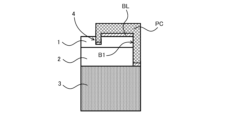
- FIG. 13 is a diagram showing an example in which a groove 4 is disposed in the vicinity of a first side surface B1.
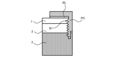
- FIG. 13A and 13B are diagrams showing an example of forming irregularities on the surface of the first side surface B1.
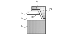
- 13 is a diagram showing an example in which the first side surface B1 is configured as an inclined surface.
- FIG. 1 is a plan view showing an optical modulation device and an optical transmission device according to the present invention.
- the present invention is characterized in that in an optical waveguide element having a composite substrate comprising a thin plate 1 forming an optical waveguide 10 and a holding substrate 4 to which the thin plate is bonded via an intermediate layer 2, a step is formed on a part of a side of the composite substrate, and in the step, the position of a first side B1 including the thin plate 1 is retreated toward the inside of the composite substrate from the position of a second side B2 including the holding substrate 3, and a protective film PC is arranged on the first side B1.
- substrates various materials can be used, including substrates with electro-optical effects such as LN, lithium tantalate, lead lanthanum zirconate titanate (PLZT), vapor-deposited films made from these materials, and even semiconductor materials and organic materials.
- substrates with electro-optical effects such as LN, lithium tantalate, lead lanthanum zirconate titanate (PLZT), vapor-deposited films made from these materials, and even semiconductor materials and organic materials.
- PZT lead lanthanum zirconate titanate
- the optical waveguide As a method for forming the optical waveguide, it is possible to use a rib-type optical waveguide in which the part of the substrate corresponding to the optical waveguide is convex by etching the surface of the substrate other than the optical waveguide and forming grooves on both sides of the optical waveguide, and it is also possible to use a horizontal slot waveguide in which a slot waveguide structure is formed in the thickness direction by thinning the substrate, thereby reducing bending loss. It is also possible to form an optical waveguide by forming a high refractive index portion on the substrate surface using titanium (Ti) or the like by thermal diffusion or proton exchange. It is also possible to form a composite optical waveguide by diffusing a high refractive index material into a rib-type optical waveguide portion. In particular, when the optical waveguide element itself is made small or a folded optical waveguide is used, a convex waveguide with a width or height of about 1 ⁇ m that provides strong light confinement is used.
- the substrate on which the optical waveguide is formed is thinned by grinding and polishing to a thickness of 10 ⁇ m or less, more preferably 5 ⁇ m or less, and even more preferably less than 1 ⁇ m (the lower limit of the thickness is preferably 0.3 ⁇ m or more), or a thinned substrate is produced using the smart cut method (a method of thinning by ion implantation peeling).
- the height of the rib-type optical waveguide is preferably set to 1 ⁇ m or less. It is also possible to form a vapor-grown film on another substrate with a thickness of about the same as the above-mentioned substrate, and process the film into the shape of the above-mentioned optical waveguide.
- a substrate (thin plate, thin film) 1 on which an optical waveguide is formed is adhesively fixed to a holding substrate 3 via an intermediate layer 2.
- a substrate in which the thin plate 1, intermediate layer 2, and holding substrate 3 are integrated is called a "composite substrate.”
- the support substrate 3 may be made of Si having a thickness of 0.2 to 1.0 mm, a glass material with a low dielectric constant, alpha quartz single crystal, quartz, sapphire, or the like.
- the intermediate layer is made of a material having a lower refractive index than the thin plate 1.
- the intermediate layer is preferably thicker than the optical waveguide substrate, 10 ⁇ m or less.
- the optical waveguide element of the present invention is characterized in that a protective film PC is formed on the first side B1 including the thin plate 1, as shown in Figures 5 and 6.
- Figure 5 is a plan view of the optical waveguide element, and to make the drawing easier to see, the optical waveguide is not shown, but as shown in Figure 6, a rib-type optical waveguide 10 is disposed between the signal electrode ES and the ground electrodes (EG1, EG2).
- FIG. 6 is an example of a cross-sectional view taken along dashed line A-A' in FIG. 5, in which a protective film PC is disposed on the first side B1 including the thin plate 1 on which the optical waveguide 10 is formed.
- the thin plate 1 and intermediate layer 2 in the portion to be cut are removed in advance by dry etching, and a protective film PC having a thickness of 1 ⁇ m or more is formed to cover the removed side B1 and to avoid contact with the blade used during cutting.
- the lower end of the protective film PC can also be positioned midway through the intermediate layer 2 or inside the holding substrate 3.
- the material used for the protective film PC can be a material used only for the protective film, but since functional layers such as electrodes and spot size converters are formed on the thin plate 1, it is also possible to use a material used for these functional layers.
- a material used for these functional layers if it is an organic dielectric, a resist-like resin with a small Young's modulus and easy patterning is preferable, and materials such as polyamide-based resins, melamine-based resins, phenol-based resins, amino-based resins, and epoxy-based resins can be used.
- the protective film is formed before forming functional layers such as electrodes, it is possible to prevent over-etching of the intermediate layer that can occur in the subsequent wet etching process.
- a material that can withstand the chemicals used in wet etching such as tantalum, gold (Au), silver, aluminum, or Si, is selected.
- an adhesion layer BL can be formed on part of the interface between the protective film PC and these substrates. This adhesion layer can also be formed on the bottom surface of the step between the first side B1 and the second side B2 to further improve adhesion.
- the material used for the adhesion layer BL depends on the material used for the protective film PC, but for example, when Au is used for the protective film PC, Ti, niobium (Nb), nickel, chromium, etc. can be used for the adhesion layer. In particular, when Ti or Nb is used, not only does it improve adhesion to the protective film, but it also has excellent corrosion resistance to iodine, which is an etchant for Au.
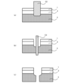
- FIG. 7A and 7B are diagrams showing an example of cutting a chip using a protective film PC.
- the thin plate 1 and the intermediate layer 2 are removed by dry etching.
- a protective film PC is formed on the first side B1.
- FIG. 7(c) when cutting the holding substrate 3 with the blade C4, the position of the blade C4 is adjusted so as not to catch the protective film PC, and cutting is performed in one step, which can suppress peeling and cracking of the thin plate 1, the intermediate layer 2, and the functional layer (not shown) formed on the thin plate. It is also possible to shorten the processing time. As shown in FIG.
- cutting can be performed at a position close to the protective film PC, and damage to the inside of the composite substrate can be suppressed by the cutting, so that the effective area of the chip can be secured widely.
- cutting is performed with the blade C4, but a wider effective area can be secured by cutting using a laser.
- the protective film PC can be formed to cover from the first side B1 to a portion of the top surface of the thin plate 1. This makes it possible to widen the area that can be protected by the protective film PC, and also to increase the adhesion between the protective film PC and the thin plate 1, etc.
- the protective film PC can be formed over the entire first side B1 including the thin plate 1, but it is also possible to form the protective film PC continuously or discontinuously around the periphery of the chip. Forming it continuously enhances the protective effect.
- a protective layer does not need to be formed because the end face is polished after cutting.
- FIG. 8 is a cross-sectional view showing an application example of FIG. 6, in which the protective film PC is formed integrally with the electrode (particularly the ground electrode EG1).
- the protective film can function as a ground electrode, ensuring a larger effective area within the chip.
- FIG. 9 shows the formation of a groove 4 on the surface of the composite substrate (thin plate 1) near the first side B1 on which the protective film PC is formed.
- This groove can suppress the progression of damage to the inside of the thin plate in the unlikely event that the thin plate 1 peels off. Furthermore, by positioning the protective film so that the protective film PC fits into the groove 4, the bonding strength of the protective film to the thin plate can be increased due to the anchor effect.
- the surface of the first side B1 on which the protective film PC is disposed is uneven.
- the first side B1 is inclined so that the surface faces upward.
- the adhesion layer BL can be laminated thicker in proportion to the inclination, and the adhesion layer BL can be reliably formed on the first side B1.
- the protective film PC can also be formed thick, improving the protective function of the thin plate and intermediate layer.
- a compact optical modulation device MD can be provided by housing the optical waveguide element (substrate 1) of the present invention in a housing CA made of metal or the like and connecting the outside of the housing to the optical waveguide element with an optical fiber F.
- a housing CA made of metal or the like
- reference numeral 5 denotes a reinforcing member superimposed on substrate 1 along the end face of substrate 1, and is used when directly joining an optical component such as an optical fiber to the end face of substrate 1.
- An electronic circuit that outputs a modulation signal S0 that causes the optical modulation device MD to perform a modulation operation can be connected to the optical modulation device MD to configure an optical transmission device OTA. Since the modulation signal S to be applied to the optical waveguide element needs to be amplified, a driver circuit DRV is used.
- the driver circuit DRV and the digital signal processor DSP can be placed outside the housing CA, but can also be placed inside the housing CA. In particular, by placing the driver circuit DRV inside the housing, the propagation loss of the modulation signal from the driver circuit can be further reduced and a wider bandwidth can be achieved.
- an optical waveguide element that suppresses peeling and cracking of thin plates and intermediate layers in a composite substrate, suppresses increases in the time required for cutting, and ensures a large effective area within the chip. It is also possible to provide an optical modulation device and an optical transmission device that use an optical waveguide element that has such excellent effects.
Landscapes
- Physics & Mathematics (AREA)
- Nonlinear Science (AREA)
- General Physics & Mathematics (AREA)
- Optics & Photonics (AREA)
- Engineering & Computer Science (AREA)
- Microelectronics & Electronic Packaging (AREA)
- Optical Integrated Circuits (AREA)
Abstract
本発明は、光導波路(10)を形成した薄板(1)と、薄板(1)を中間層(2)を介して接合した保持基板(4)とを備える複合基板を有する光導波路素子において、複合基板の側面の一部には段差が形成され、段差では、薄板(1)を含む第1側面(B1)の位置が、保持基板(3)を含む第2側面(B2)の位置から複合基板の内側方向に退避しており、第1側面(B1)に保護膜(PC)が配置されていることを特徴とする。
Description
本発明は、光導波路素子とそれを用いた光変調デバイス並びに光送信装置に関し、特に、光導波路を形成した薄板と、該薄板を中間層を介して接合した保持基板とを備える複合基板を有する光導波路素子に関する。
光通信分野や光計測分野において、ニオブ酸リチウム(LN)等の電気光学効果を有する基板に光導波路を形成し、光導波路を伝搬する光波を変調する変調電極を備えた光変調器等の光導波路素子が多用されている。
HB-CDM(High Bandwidth Coherent Driver Modulator)等のドライバ集積型変調器では、光導波路素子を駆動するドライバ回路を光導波路素子と一緒に筐体内に組み込み、さらに全体のパッケージを小型化すること等が求められている。このため、光導波路素子自体も小型化し、1μm程度の幅や高さを有するリブ型光導波路を形成した薄板が利用されている。光導波路を形成する薄板の機械的強度を高めるため、薄板を保持する保持基板が使用され、さらに、薄板と保持基板との密着性を高めるため中間層を設けた複合基板が利用されている。さらに、薄板上には電極等の機能層が形成された後に、ウエハ状態から個々の光導波路素子のチップに切り出しが行われている。
具体的には、薄板としては1μm以下のLN等の電気光学効果を有する基板が利用され、保持基板には機械的強度を補強するため、厚さ0.2~1.0mmのシリコン(Si)やアルファ石英単結晶等が利用される。中間層としては10μm以下で接合強度を高めることができるもの、例えば、LN薄板とSi基板の接合にはSi酸化膜等が好適に使われる。
保持基板の材質を半導体分野で多用しているSiとすることで、切断条件が確立しており、外周刃(ブレード)を用いた高品質な切削が可能となっている。一方、広帯域変調器では、誘電特性の向上を図るため、誘電率の低いガラス材やアルファ石英単結晶、水晶、サファイア等を保持基板に適用することも検討されている。これらは、一般的にSiに比べ被削性率(削られ易さ)が低い傾向にあり、単一のブレード切断では、薄板や中間層の切断面の品質維持が困難となる。
例えば、図1(a)のように、薄板1、中間層2及び保持基板3の複合基板をブレードC1を利用して切断する。この場合には、加工中に発生する摩擦熱やブレード砥粒の摩耗、脱落、それらを抑制するための切削液の影響により、図1(b)に示すように、薄板や中間層が剥がれたり、チッピングや欠けが発生し、それを起点にクラックへと進行することがある。
また、光導波路素子は、通信高速化に加え小型化の要求も高まり、チップ上に緻密な導波路及び電極等の機能層を形成することになる。これらを形成する上で、チップ表面積をできるだけ広く確保する必要があるが、薄板等の剥がれを考慮した設計では、同じチップサイズでは有効面積が狭くなる。
図2はベベルカット又はステップカット方式と呼ばれるもので、2種類のブレード(C2,C3)を用意して切断を行うものである。図1のような1回の切断工程での切断に比べ、図2では1回目の切込み(図2(a)参照)を浅くすることができる。このため、各層に適した切断ブレードを使い分けることで、薄板や中間層の剥がれ及びクラックを抑制することができる。しかしながら、切断回数が増えることで、切断加工に掛かる時間が増加するという問題を生ずる。
また、特許文献1では、図3に示すように、チップ切断面の内側の上面に溝4を入れる方式も提案されている。溝4が防波堤の役割を持ち、切断した際に図3(b)に示すように、薄板や中間層の剥がれ及びクラックの基板内部への進行を抑制することができるが、溝4を形成した幅の分だけ、チップとしての有効面積が狭くなるという問題がある。
特許文献2では、複合基板の上部を、予めドライエッチング(図4(a)参照)及びウェットエッチング(図4(b)参照)により除去し、除去した部分に沿って、レーザー照射あるいは結晶劈開面により分断すること(図4(c)参照)が開示されている。この切断方式では、ブレード切断に比べ、加工面が高品質であり、切断幅が狭くチップ内の有効面積を広く確保することができるが、図4(b)に示すように、ウェットエッチング中に薄板や中間層の剥がれや、アンダー(オーバー)エッチングが発生する。
本発明が解決しようとする課題は、上述したような問題を解決し、複合基板における薄板や中間層の剥がれ及びクラックの発生を抑制すると共に、切断加工に係る時間の増加を抑制し、かつチップ内の有効面積を広く確保することを可能とする光導波路素子を提供することである。また、この光導波路素子を用いた光変調デバイス及び光送信装置を提供することである。
上記課題を解決するため、本発明の光導波路素子、光変調デバイス、及び光送信装置は、以下のような技術的特徴を有する。
(1) 光導波路を形成した薄板と、該薄板を中間層を介して接合した保持基板とを備える複合基板を有する光導波路素子において、該複合基板の側面の一部には段差が形成され、該段差では、該薄板を含む第1側面の位置が、該保持基板を含む第2側面の位置から該複合基板の内側方向に退避しており、該第1側面に保護膜が配置されていることを特徴とする。
(1) 光導波路を形成した薄板と、該薄板を中間層を介して接合した保持基板とを備える複合基板を有する光導波路素子において、該複合基板の側面の一部には段差が形成され、該段差では、該薄板を含む第1側面の位置が、該保持基板を含む第2側面の位置から該複合基板の内側方向に退避しており、該第1側面に保護膜が配置されていることを特徴とする。
(2) 上記(1)に記載の光導波路素子において、該保護膜は、該第1側面から該薄板の上面の一部までを覆うように形成されていることを特徴とする。
(3) 上記(1)に記載の光導波路素子において、該保護膜と該複合基板との界面の一部には密着層が配置されていることを特徴とする。
(4) 上記(1)に記載の光導波路素子において、該複合基板には、該第1側面よりさらに該複合基板の内側の位置に溝が形成されていることを特徴とする。
(5) 上記(1)に記載の光導波路素子において、該第1側面の表面には凹凸が形成されていることを特徴とする。
(6) 上記(1)に記載の光導波路素子において、該第1側面は、上方に面が向くように傾斜していることを特徴とする。
(7) 上記(1)乃至(6)のいずれかに記載の光導波路素子と、該光導波路素子を収容する筐体と、該光導波路素子に光波を入出力する光ファイバとを有することを特徴とする光変調デバイスである。
(8) 上記(7)に記載の光変調デバイスにおいて、該光導波路を伝搬する光波を変調する変調電極を該基板に設け、該変調電極に入力する変調信号を増幅する電子回路を該筐体の内部又は外部に有することを特徴とする。
(9) 上記(8)に記載の光変調デバイスと、該光変調デバイスに変調動作を行わせる変調信号を出力する電子回路とを有することを特徴とする光送信装置である。
本発明により、光導波路を形成した薄板と、該薄板を中間層を介して接合した保持基板とを備える複合基板を有する光導波路素子において、該複合基板の側面の一部には段差が形成され、該段差では、該薄板を含む第1側面の位置が、該保持基板を含む第2側面の位置から該複合基板の内側方向に退避しており、該第1側面に保護膜が配置されているため、第1側面の保護膜で保護し、第2側面での切断に際して第1側面が損傷することが効果的に抑制される。薄板や中間層等薄板を含む部分の切断には、薄板等の剥がれ及びクラックの発生を抑制する手法を採用し、その後、第1側面を保護膜で覆うため、保持基板を含む部分の切断には、効率的な切断手法が採用でき、切断加工に係る時間の増加を抑制することが可能となる。しかも、第1側面での損傷が抑制されるため、チップ内の有効面積を広く確保することも可能となる光導波路素子を提供することができる。また、この優れた効果を奏する光導波路素子を用いた光変調デバイス及び光送信装置も提供することが可能となる。
以下、本発明について好適例を用いて詳細に説明する。
本発明は、図5及び図6に示すように、光導波路10を形成した薄板1と、該薄板を中間層2を介して接合した保持基板4とを備える複合基板を有する光導波路素子において、該複合基板の側面の一部には段差が形成され、該段差では、該薄板1を含む第1側面B1の位置が、該保持基板3を含む第2側面B2の位置から該複合基板の内側方向に退避しており、該第1側面B1に保護膜PCが配置されていることを特徴とする。
本発明は、図5及び図6に示すように、光導波路10を形成した薄板1と、該薄板を中間層2を介して接合した保持基板4とを備える複合基板を有する光導波路素子において、該複合基板の側面の一部には段差が形成され、該段差では、該薄板1を含む第1側面B1の位置が、該保持基板3を含む第2側面B2の位置から該複合基板の内側方向に退避しており、該第1側面B1に保護膜PCが配置されていることを特徴とする。
基板1としては、LNやタンタル酸リチウム、ジルコン酸チタン酸鉛ランタン(PLZT)等の電気光学効果を有する基板や、これらの材料による気相成長膜、さらには、半導体材料や有機材料等種々の材料も利用可能である。
光導波路の形成方法としては、光導波路以外の基板表面をエッチングし、光導波路の両側に溝を形成する等、基板の光導波路に対応する部分を凸状としたリブ型光導波路を利用することが可能であり、基板の薄膜化により厚さ方向にスロット導波路構造を形成する水平スロット導波路を使用することにより、曲げ損失の低減が可能となる。
また、チタニウム(Ti)等を熱拡散法やプロトン交換法等で基板表面に高屈折率部分を形成することで光導波路を形成することも可能である。リブ型光導波路部分に高屈折率材料を拡散する等、複合的な光導波路を形成することも可能である。特に、光導波路素子自体を小型化する場合や折り曲げた光導波路を使用する場合等には、光閉じ込めの強い、幅又は高さが1μm程度の凸状導波路を用いる。
また、チタニウム(Ti)等を熱拡散法やプロトン交換法等で基板表面に高屈折率部分を形成することで光導波路を形成することも可能である。リブ型光導波路部分に高屈折率材料を拡散する等、複合的な光導波路を形成することも可能である。特に、光導波路素子自体を小型化する場合や折り曲げた光導波路を使用する場合等には、光閉じ込めの強い、幅又は高さが1μm程度の凸状導波路を用いる。
光導波路を形成した基板は、変調信号のマイクロ波と光波との速度整合を図るため、10μm以下、より好ましくは5μm以下、更に好ましくは1μm未満の厚さ(厚さの下限は0.3μm以上が好ましい)まで研削研磨により薄板化する方法と、スマートカット法(イオン注入剥離により薄膜化する方法)を用いて薄膜化基板を作製する。リブ型光導波路の高さは、1μm以下に設定することが好ましい。また、他の基板上に気相成長膜を上述の基板の厚さ程度で形成し、当該膜を上述のような光導波路の形状に加工することも可能である。
光導波路を形成した基板(薄板、薄膜)1は、機械的強度を高めるため、中間層2を介して、保持基板3に接着固定される。本発明では、薄板1、中間層2及び保持基板3を一体化した基板を「複合基板」という。
保持基板3には、厚さ0.2~1.0mmのSiや誘電率の低いガラス材や、アルファ石英単結晶、水晶、サファイア等が利用可能である。
また、中間層には、光波と電気信号(マイクロ波)との速度整合を図るため、薄板1よりも屈折率の低い材料が使用される。また、薄板1に熱応力が加わるのを抑制するため、熱膨張率が薄板1に近い材料が好ましく、例えば、二酸化ケイ素、窒化ケイ素、酸化アルミニウム、フッ化マグネシウム、酸化ランタン、酸化亜鉛、酸化マグネシウム、フッ化カルシウム、酸化イットリウム等を用いることが可能である。また、接着強度を維持するため、光導波路基板よりも厚く、10μm以下であることが好ましい。
保持基板3には、厚さ0.2~1.0mmのSiや誘電率の低いガラス材や、アルファ石英単結晶、水晶、サファイア等が利用可能である。
また、中間層には、光波と電気信号(マイクロ波)との速度整合を図るため、薄板1よりも屈折率の低い材料が使用される。また、薄板1に熱応力が加わるのを抑制するため、熱膨張率が薄板1に近い材料が好ましく、例えば、二酸化ケイ素、窒化ケイ素、酸化アルミニウム、フッ化マグネシウム、酸化ランタン、酸化亜鉛、酸化マグネシウム、フッ化カルシウム、酸化イットリウム等を用いることが可能である。また、接着強度を維持するため、光導波路基板よりも厚く、10μm以下であることが好ましい。
本発明の光導波路素子の特徴は、図5及び図6に示すように、薄板1を含む第1側面B1に保護膜PCを形成することである。図5は、光導波路素子の平面図であり、図面を見易くするため、光導波路は図示していないが、図6に示すように、信号電極ESと接地電極(EG1,EG2)との間にはリブ型光導波路10が配置されている。
図6は、図5の一点鎖線A-A’における断面図の一例であり、光導波路10が形成された薄板1を含む第1側面B1には保護膜PCが配置されている。切断する部分の薄板1及び中間層2を、予めドライエッチングにより除去し、除去した側面B1を覆うように、かつ切断時に使用するブレードに掛からないように1μm以上の厚みの保護膜PCを形成する。なお、保護膜PCの下端は、中間層2の途中又は保持基板3の内部に入り込むように位置させることも可能である。
保護膜PCに使用する材料は、保護膜のみに使用される材料を用いることも可能であるが、薄板1上には電極やスポットサイズ変換器等の機能層が形成されるため、この機能層に使用する材料を用いることも可能である。また、有機誘電体であればレジストのような樹脂で、ヤング率が小さく、パターンニングしやすいものが好ましく、例えば、ポリアミド系樹脂、メラミン系樹脂、フェノール系樹脂、アミノ系樹脂、エポキシ系樹脂等の材料を用いることが可能である。これらの機能層の形成工程と同時に保護膜を形成することで生産プロセスが複雑化することも抑制できる。
保護膜の形成を、電極等の機能層を形成する前に行えば、後工程のウェットエッチングで起こりうる中間層のオーバーエッチングを抑制することができる。その場合、ウェットエッチングによる薬液に耐える材質、例えば、タンタル、金(Au)、銀、アルミニウム、Si等が選定される。
保護膜が薄板1や保持基板3又は中間層2との密着性が低い場合には、保護膜PCとこれらの基板との界面の一部に密着層BLを形成することができる。この密着層は、第1側面B1と第2側面B2との間にある段差底面にも形成することで、より密着性を高めることができる。密着層BLに使用する材料は、保護膜PCに使用する材料にも依存するが、例えば、Auを保護膜PCに使用する場合には、Tiやニオブ(Nb)、ニッケル、クロム等を密着層に用いることが可能である。特にTiやNb等を使用した場合には、保護膜との密着性を上げるだけでなく、Auのエッチャントであるヨウ素等に対して優れた耐食性がある。
図7は保護膜PCを用いてチップを切断する例を示す図である。図7(a)に示すように、ドライエッチングで薄板1及び中間層2を除去する。次に、図7(b)のように保護膜PCを第1側面B1に形成する。その際に予め密着層BLを形成することも可能である。
図7(c)に示すように、ブレードC4により保持基板3を切断する際には、保護膜PCに掛からないようにブレードC4の位置を調整し、1回の工程で切断することで、薄板1や中間層2、薄板上に形成する機能層(不図示)の剥がれ及びクラックの発生を抑制することができる。また、加工に係る時間も短縮することが可能である。図7(d)のように、保護膜PCに近い位置を切断でき、当該切断により複合基板内部への損傷も抑制できるため、チップの有効面積を広く確保することが可能となる。図7では、ブレードC4により切断を行ったが、レーザーを使用して切断することで、有効面積をより広く確保することもできる。
図7(c)に示すように、ブレードC4により保持基板3を切断する際には、保護膜PCに掛からないようにブレードC4の位置を調整し、1回の工程で切断することで、薄板1や中間層2、薄板上に形成する機能層(不図示)の剥がれ及びクラックの発生を抑制することができる。また、加工に係る時間も短縮することが可能である。図7(d)のように、保護膜PCに近い位置を切断でき、当該切断により複合基板内部への損傷も抑制できるため、チップの有効面積を広く確保することが可能となる。図7では、ブレードC4により切断を行ったが、レーザーを使用して切断することで、有効面積をより広く確保することもできる。
図6及び図7(d)に示すように、保護膜PCは、第1側面B1から薄板1の上面の一部までを覆うように形成することが可能である。これにより、保護膜PCで保護できる範囲を広くすることができると共に、保護膜PCと薄板1等の密着性も高くすることが可能となる。
保護膜PCを形成する範囲は、薄板1を含む第1側面B1の全面に形成することが可能であるが、チップ外周に連続又は不連続で保護膜PCを形成することも可能である。連続して形成することで保護効果が高まる。ただし、光導波路端部が形成される面については、切断後に端面を研磨するため、保護層を形成しなくてもよい。例えば、図5の図面の右側面には保護膜を形成しない部分を設けることも可能である。これは、光導波路を折り返すパターンを有する光導波路素子では、光導波路へ光波を入力または光波を出力する側がこの右側面に形成されているためである。
図8は、図6の応用例を示す断面図であり、保護膜PCを電極(特に接地電極EG1)と一体的に形成したものである。保護膜を電極と同材質、例えばAuで形成し、さらに、保護膜PCと接地電極を電気的に接続することで、保護層を接地電極として機能させることができ、チップ内の有効面積をより広く確保することができる。
図9は、保護膜PCを形成した第1側面B1の近傍の複合基板(薄板1)の表面に溝4形成するものである。この溝は、万が一、薄板1が剥離した際の薄板内部への損傷の進行を抑制することができる。しかも、溝4に保護膜PCが入り込むように保護膜を配置することで、アンカー効果により、保護膜の薄板への接合強度を高めることができる。
図10は、保護膜PCが配置される第1側面B1の表面に凹凸を形成している。この凹凸に合わせて保護膜PCが配置されることで、第1側面と保護膜との接触面積を増加し、両者の接合強度を高めることが可能となる。
図11は、第1側面B1を、上方に表面が向くように傾斜させたものである。スパッタや蒸着等で密着層BLを形成する際に、傾斜している分だけ密着層を厚く積層させることができ、第1側面B1にも確実に密着層BLを形成することができる。また、保護膜PCについても同様に膜厚を厚く形成することができ、薄板や中間層の保護機能を高めることができる。
図12に示すように、本発明の光導波路素子(基板1)を金属等の筐体CA内に収容し、筐体の外部と光導波路素子とを光ファイバFで接続することで、コンパクトな光変調デバイスMDを提供することができる。当然、基板1の光導波路の入射部又は出射部に光ファイバを直接接続するだけでなく、空間光学系を介して光学的に接続することも可能である。なお、符号5は、基板1の端面に沿って基板1に重ね合わせた補強部材であり、光ファイバ等の光学部品を基板1の端面に直接接合する際に使用される。
光変調デバイスMDに変調動作を行わせる変調信号S0を出力する電子回路(デジタル信号プロセッサーDSP)を、光変調デバイスMDに接続することにより、光送信装置OTAを構成することが可能である。光導波路素子に印加する変調信号Sは増幅する必要があるため、ドライバ回路DRVが使用される。ドライバ回路DRVやデジタル信号プロセッサーDSPは、筐体CAの外部に配置することも可能であるが、筐体CA内に配置することも可能である。特に、ドライバ回路DRVを筐体内に配置することで、ドライバ回路からの変調信号の伝搬損失をより低減し広帯域化が可能となる。
以上のように、本発明によれば、複合基板における薄板や中間層の剥がれ及びクラックの発生を抑制すると共に、切断加工に係る時間の増加を抑制し、かつチップ内の有効面積を広く確保することを可能とする光導波路素子を提供することが可能となる。また、このような優れた効果を有する光導波路素子を用いた光変調デバイス及び光送信装置を提供することができる。
1 薄板
2 中間層
3 保持基板
4 溝
PC 保護膜
BL 密着層
B1 第1側面
B2 第2側面
2 中間層
3 保持基板
4 溝
PC 保護膜
BL 密着層
B1 第1側面
B2 第2側面
Claims (9)
- 光導波路を形成した薄板と、該薄板を中間層を介して接合した保持基板とを備える複合基板を有する光導波路素子において、
該複合基板の側面の一部には段差が形成され、該段差では、該薄板を含む第1側面の位置が、該保持基板を含む第2側面の位置から該複合基板の内側方向に退避しており、
該第1側面に保護膜が配置されていることを特徴とする光導波路素子。 - 請求項1に記載の光導波路素子において、該保護膜は、該第1側面から該薄板の上面の一部までを覆うように形成されていることを特徴とする光導波路素子。
- 請求項1に記載の光導波路素子において、該保護膜と該複合基板との界面の一部には密着層が配置されていることを特徴とする光導波路素子。
- 請求項1に記載の光導波路素子において、該複合基板には、該第1側面よりさらに該複合基板の内側の位置に溝が形成されていることを特徴とする光導波路素子。
- 請求項1に記載の光導波路素子において、該第1側面の表面には凹凸が形成されていることを特徴とする光導波路素子。
- 請求項1に記載の光導波路素子において、該第1側面は、上方に面が向くように傾斜していることを特徴とする光導波路素子。
- 請求項1乃至6のいずれかに記載の光導波路素子と、該光導波路素子を収容する筐体と、該光導波路素子に光波を入出力する光ファイバとを有することを特徴とする光変調デバイス。
- 請求項7に記載の光変調デバイスにおいて、該光導波路を伝搬する光波を変調する変調電極を該基板に設け、該変調電極に入力する変調信号を増幅する電子回路を該筐体の内部又は外部に有することを特徴とする光変調デバイス。
- 請求項8に記載の光変調デバイスと、該光変調デバイスに変調動作を行わせる変調信号を出力する電子回路とを有することを特徴とする光送信装置。
Priority Applications (1)
| Application Number | Priority Date | Filing Date | Title |
|---|---|---|---|
| PCT/JP2023/013083 WO2024201864A1 (ja) | 2023-03-30 | 2023-03-30 | 光導波路素子とそれを用いた光変調デバイス並びに光送信装置 |
Applications Claiming Priority (1)
| Application Number | Priority Date | Filing Date | Title |
|---|---|---|---|
| PCT/JP2023/013083 WO2024201864A1 (ja) | 2023-03-30 | 2023-03-30 | 光導波路素子とそれを用いた光変調デバイス並びに光送信装置 |
Publications (1)
| Publication Number | Publication Date |
|---|---|
| WO2024201864A1 true WO2024201864A1 (ja) | 2024-10-03 |
Family
ID=92903692
Family Applications (1)
| Application Number | Title | Priority Date | Filing Date |
|---|---|---|---|
| PCT/JP2023/013083 Ceased WO2024201864A1 (ja) | 2023-03-30 | 2023-03-30 | 光導波路素子とそれを用いた光変調デバイス並びに光送信装置 |
Country Status (1)
| Country | Link |
|---|---|
| WO (1) | WO2024201864A1 (ja) |
Citations (6)
| Publication number | Priority date | Publication date | Assignee | Title |
|---|---|---|---|---|
| US20040066250A1 (en) * | 2000-08-25 | 2004-04-08 | Hunt Andrew T | Electronic and optical devices and methods of forming these devices |
| JP2004295118A (ja) * | 2003-03-12 | 2004-10-21 | Sanyo Electric Co Ltd | 光導波路 |
| JP2008140829A (ja) * | 2006-11-30 | 2008-06-19 | Sharp Corp | 半導体装置およびその製造方法 |
| US20150214077A1 (en) * | 2014-01-24 | 2015-07-30 | Taiwan Semiconductor Manufacturing Company, Ltd. | Methods of Packaging and Dicing Semiconductor Devices and Structures Thereof |
| JP2021105658A (ja) * | 2019-12-26 | 2021-07-26 | 住友大阪セメント株式会社 | 光導波路デバイス |
| JP2022142650A (ja) * | 2021-03-16 | 2022-09-30 | 富士通オプティカルコンポーネンツ株式会社 | 光デバイス、光通信装置及び光デバイスの製造方法 |
-
2023
- 2023-03-30 WO PCT/JP2023/013083 patent/WO2024201864A1/ja not_active Ceased
Patent Citations (6)
| Publication number | Priority date | Publication date | Assignee | Title |
|---|---|---|---|---|
| US20040066250A1 (en) * | 2000-08-25 | 2004-04-08 | Hunt Andrew T | Electronic and optical devices and methods of forming these devices |
| JP2004295118A (ja) * | 2003-03-12 | 2004-10-21 | Sanyo Electric Co Ltd | 光導波路 |
| JP2008140829A (ja) * | 2006-11-30 | 2008-06-19 | Sharp Corp | 半導体装置およびその製造方法 |
| US20150214077A1 (en) * | 2014-01-24 | 2015-07-30 | Taiwan Semiconductor Manufacturing Company, Ltd. | Methods of Packaging and Dicing Semiconductor Devices and Structures Thereof |
| JP2021105658A (ja) * | 2019-12-26 | 2021-07-26 | 住友大阪セメント株式会社 | 光導波路デバイス |
| JP2022142650A (ja) * | 2021-03-16 | 2022-09-30 | 富士通オプティカルコンポーネンツ株式会社 | 光デバイス、光通信装置及び光デバイスの製造方法 |
Similar Documents
| Publication | Publication Date | Title |
|---|---|---|
| JP4443011B2 (ja) | 進行波型光変調器 | |
| WO2005019913A1 (ja) | 光導波路デバイスおよび進行波形光変調器 | |
| WO2007122877A1 (ja) | 光変調素子 | |
| US9298025B2 (en) | Electrode structure for an optical waveguide substrate | |
| JP7452190B2 (ja) | 光導波路素子及びそれを用いた光変調デバイス並びに光送信装置 | |
| CN115280227B (zh) | 光波导元件、使用该光波导元件的光调制器件及光发送装置 | |
| JP2004341147A (ja) | 光導波路デバイスおよび進行波形光変調器 | |
| WO2024201864A1 (ja) | 光導波路素子とそれを用いた光変調デバイス並びに光送信装置 | |
| JP2007101641A (ja) | 光変調器及びその製造方法 | |
| JP5494400B2 (ja) | 光導波路素子 | |
| JP2013080007A (ja) | 光導波路素子 | |
| JP7346876B2 (ja) | 光導波路素子 | |
| CN120266046A (zh) | 光波导元件、光调制器及光发送装置 | |
| JP2003270600A (ja) | 光変調器の製造方法 | |
| WO2023188311A1 (ja) | 光導波路素子及びそれを用いた光変調デバイス並びに光送信装置 | |
| WO2003079102A1 (fr) | Procede de fabrication de modulateur optique | |
| EP1500965A1 (en) | Optical waveguide device with optical modulator and manufacturing method therefor | |
| CN103842866B (zh) | 光波导器件及其制造方法 | |
| WO2024069953A1 (ja) | 光変調器及びそれを用いた光送信装置 | |
| WO2025069276A1 (ja) | 光導波路素子及びそれを用いた光変調デバイス並びに光送信装置 | |
| WO2023188174A1 (ja) | 光導波路素子及びそれを用いた光変調デバイス並びに光送信装置 | |
| JP4671335B2 (ja) | 導波路型光デバイス | |
| JPH0756036A (ja) | 光導波路デバイス及びその製造方法 | |
| JP6144770B2 (ja) | 光学部品 | |
| WO2024075277A1 (ja) | 光導波路素子及びそれを用いた光変調器並びに光送信装置 |
Legal Events
| Date | Code | Title | Description |
|---|---|---|---|
| 121 | Ep: the epo has been informed by wipo that ep was designated in this application |
Ref document number: 23930502 Country of ref document: EP Kind code of ref document: A1 |
|
| NENP | Non-entry into the national phase |
Ref country code: DE |
|
| 122 | Ep: pct application non-entry in european phase |
Ref document number: 23930502 Country of ref document: EP Kind code of ref document: A1 |