WO2024201675A1 - 光受信装置及び信号処理方法 - Google Patents
光受信装置及び信号処理方法 Download PDFInfo
- Publication number
- WO2024201675A1 WO2024201675A1 PCT/JP2023/012293 JP2023012293W WO2024201675A1 WO 2024201675 A1 WO2024201675 A1 WO 2024201675A1 JP 2023012293 W JP2023012293 W JP 2023012293W WO 2024201675 A1 WO2024201675 A1 WO 2024201675A1
- Authority
- WO
- WIPO (PCT)
- Prior art keywords
- optical
- waveform
- signal
- unit
- electrical signal
- Prior art date
- Legal status (The legal status is an assumption and is not a legal conclusion. Google has not performed a legal analysis and makes no representation as to the accuracy of the status listed.)
- Ceased
Links
Images







Classifications
-
- H—ELECTRICITY
- H04—ELECTRIC COMMUNICATION TECHNIQUE
- H04B—TRANSMISSION
- H04B10/00—Transmission systems employing electromagnetic waves other than radio-waves, e.g. infrared, visible or ultraviolet light, or employing corpuscular radiation, e.g. quantum communication
- H04B10/07—Arrangements for monitoring or testing transmission systems; Arrangements for fault measurement of transmission systems
- H04B10/075—Arrangements for monitoring or testing transmission systems; Arrangements for fault measurement of transmission systems using an in-service signal
- H04B10/077—Arrangements for monitoring or testing transmission systems; Arrangements for fault measurement of transmission systems using an in-service signal using a supervisory or additional signal
-
- H—ELECTRICITY
- H04—ELECTRIC COMMUNICATION TECHNIQUE
- H04B—TRANSMISSION
- H04B10/00—Transmission systems employing electromagnetic waves other than radio-waves, e.g. infrared, visible or ultraviolet light, or employing corpuscular radiation, e.g. quantum communication
- H04B10/60—Receivers
- H04B10/61—Coherent receivers
Definitions
- the present invention relates to an optical receiving device and a signal processing method.
- FIG 13 shows an example of the spectrum of an optical signal that has passed through an optical fiber transmission line and an optical amplifier and arrived at a receiver.
- the receiver receives not only the optical signal but also noise.
- P1 is the optical signal spectrum
- P2 is the noise spectrum.
- the quality of the optical signal received by the receiver is measured by the Optical to Signal and Noise Ratio (OSNR).
- OSNR is the power ratio between the optical signal and noise. OSNR is calculated using the following formula (1).
- OSNR optical signal power / noise power per 0.1 nm ... (1)
- the frequency is equivalent to about 12.5 GHz.
- an external measuring device In an environment where the OSNR of an optical fiber transmission line is to be measured, an external measuring device must be connected each time an OSNR measurement is performed. This makes the configuration and operation complicated.
- the present invention aims to provide an optical receiving device and a signal processing method that can measure the OSNR in an optical fiber transmission line while reducing the complexity of the configuration and operation.
- One aspect of the present invention is an optical receiving device that includes an optical signal receiving unit that receives a phase-modulated or quadrature amplitude-modulated optical signal generated by an optical transmitting device and converts the received optical signal into an electrical signal by coherent detection, an electrical signal processing unit that demodulates the electrical signal converted by the optical signal receiving unit, and an estimation unit that calculates a waveform consistency that quantitatively represents a match between a waveform represented by the electrical signal and a known waveform based on a demodulation result by the electrical signal processing unit, and estimates an optical signal-to-noise ratio using the calculated waveform consistency.
- One aspect of the present invention is a signal processing method having a receiving step of receiving a phase-modulated or quadrature amplitude-modulated optical signal generated by an optical transmitting device and converting the received optical signal into an electrical signal by coherent detection, a signal processing step of demodulating the electrical signal, and an estimation step of calculating a waveform consistency that quantitatively represents a match between the waveform represented by the electrical signal and a known waveform based on the demodulation result in the signal processing step, and estimating an optical signal-to-noise ratio using the calculated waveform consistency.
- the present invention makes it possible to measure the OSNR in optical fiber transmission paths while reducing the complexity of configuration and operation.
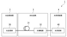
- FIG. 1 is a configuration diagram of an optical communication system according to a first embodiment of the present invention.
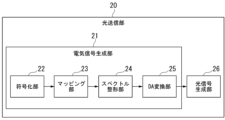
- FIG. 2 is a diagram illustrating an example of the configuration of an optical transmitting unit according to the embodiment.
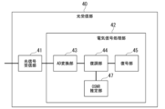
- FIG. 2 is a diagram illustrating an example of the configuration of an optical receiving unit according to the embodiment.
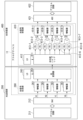
- FIG. 2 is a diagram illustrating an example of an analog device according to the embodiment.
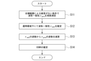
- 11 is a flowchart showing a procedure for calculating an OSNR of an optical transmission line according to the embodiment.
- FIG. 13 is a diagram showing a connection configuration for advance measurement of waveform consistency according to the embodiment.
- FIG. 11 is a diagram for explaining OSNR estimation in the second embodiment.
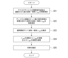
- 11 is a flowchart showing a procedure for calculating an OSNR of an optical transmission line according to the embodiment.
- FIG. 13 is a diagram showing a connection configuration for advance measurement of waveform consistency according to the embodiment.
- FIG. 13 is a diagram showing an example of a waveform consistency advance measurement according to the embodiment.
- FIG. 13 is a diagram showing a connection configuration for advance measurement of waveform consistency according to the embodiment.
- FIG. 13 is a diagram showing an example of a waveform consistency advance measurement according to the embodiment.
- FIG. 2 is a diagram illustrating an example of the spectrum of an optical signal arriving at a receiver.
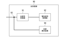
- FIG. 1 illustrates a prior art optical receiving section.
- FIG. 1 is a diagram showing an example of the configuration of an optical communication system 1 according to the present embodiment.
- the optical communication system 1 includes an optical transmitter 2, an optical transmission line 3, and an optical receiver 4.
- the optical transmitting device 2 has an optical transmitting unit 20.
- the optical transmitting unit 20 generates an optical signal and outputs the generated optical signal to the optical transmission path 3.
- the optical transmission path 3 transmits the optical signal output by the optical transmitting device 2.
- the optical signal transmitted through the optical transmission path 3 is input to the optical receiving device 4.
- the optical transmission path 3 includes an optical fiber 31, which is a transmission medium for an optical signal. If the optical transmission path 3 includes an optical fiber 31, devices such as an optical amplifier 32, an optical switch (not shown), and a regenerative repeater may be inserted along the path.
- the optical receiving device 4 has an optical receiving unit 40.
- the optical receiving unit 40 receives the optical signal transmitted by the optical transmission path 3.
- the optical receiving unit 40 measures the OSNR based on the received optical signal.
- FIG. 2 is a diagram showing an example of the configuration of the optical transmission unit 20.
- the optical transmission unit 20 may be an optical transmitter of the prior art.
- the optical transmission unit 20 has an electrical signal generation unit 21 and an optical signal generation unit 26.
- the electrical signal generating unit 21 encodes the information source and converts it into an electrical signal waveform.
- the electrical signal waveform is the waveform of a digitally modulated signal that has been converted by phase modulation or quadrature amplitude modulation.
- the electrical signal generating unit 21 includes an encoding unit 22, a mapping unit 23, a spectrum shaping unit 24, and a DA (digital-to-analog) conversion unit 25.
- the encoding unit 22 generates a transmission signal by encoding a transmission bit sequence from an information source.
- the mapping unit 23 maps the encoded transmission signal to symbols for phase modulation or quadrature amplitude modulation.
- the spectrum shaping unit 24 shapes the spectrum (waveform) of the transmission signal by sampling the symbol-mapped transmission signal.
- the spectrum shaping unit 24 may compensate for distortion of the waveform of the spectrum-shaped transmission signal by pre-equalization.
- the DA conversion unit 25 converts the transmission signal from a digital signal to an analog signal, and outputs the converted analog signal to the optical signal generation unit 26.
- FIG. 14 is a diagram showing the configuration of a conventional optical receiving unit 90.
- a conventional optical communication system has an optical receiving unit 90 shown in FIG. 14 instead of the optical receiving unit 40 shown in FIG. 1.
- the optical receiving unit 90 has an optical signal receiving unit 91, an electrical signal processing unit 92, and a branching unit 93.
- the optical signal receiving unit 91 converts the received optical signal into an electrical signal and outputs the converted electrical signal to the electrical signal processing unit 92.
- the electrical signal processing unit 92 performs digital signal reception processing on the electrical signal input from the optical signal receiving unit 91.
- the branching unit 93 and the OSNR estimation device 94 are connected by an optical fiber.
- the branching unit 93 branches a part of the optical signal input from the optical transmission path 3 to the optical signal receiving unit 91 and outputs it to the OSNR estimation device 94.
- the OSNR estimation device 94 measures the OSNR using the optical signal branched by the branching unit 93.
- FIG. 3 is a diagram showing an example of the configuration of the optical receiving unit 40.
- the optical receiving unit 40 has an optical signal receiving unit 41 and an electrical signal processing unit 42.
- the optical signal receiving unit 41 is a coherent optical receiving unit.
- the optical signal receiving unit 91 included in the conventional optical receiving unit 90 may be used as the optical signal receiving unit 41.
- the optical signal receiving unit 41 is configured with a 90-degree optical hybrid circuit, a local oscillator light source, a photodetector, and an optical fiber that couples them as a minimum unit.
- the optical signal receiving unit 41 may include other optical devices such as an optical attenuator.
- the optical signal receiving unit 41 receives an optical signal transmitted through the optical transmission path 3.
- the optical signal receiving unit 41 converts the received optical signal into an electrical signal while maintaining the phase and amplitude of the optical signal, and outputs the converted electrical signal to the electrical signal processing unit 42.
- the electrical signal processing unit 42 performs digital signal reception processing such as demodulation on the electrical signal input from the optical signal receiving unit 41.
- the digital signal reception processing performed by the electrical signal processing unit 42 may be similar to the digital signal reception performed by the electrical signal processing unit 42 of the conventional optical receiving unit 90.
- the electrical signal processing unit 42 estimates the OSNR of the optical transmission path 3 using the symbols obtained by demodulation.
- the electrical signal processing unit 42 includes an analog-to-digital (AD) conversion unit 43, a demodulation unit 44, a decoding unit 45, and an OSNR estimation unit 46.
- AD analog-to-digital
- the AD conversion unit 43 converts the received signal output by the optical signal receiving unit 41 from an analog signal to a digital signal.
- the demodulation unit 44 determines the symbol of the received signal converted to a digital signal by the AD conversion unit 43, and converts the determined symbol into binary data. Note that the demodulation unit 44 may compensate for the frequency characteristics of the optical signal receiving unit 41 and compensate for chromatic dispersion received in the optical transmission path 3 before symbol determination. Furthermore, the demodulation unit 44 may perform equalization processing on the compensated electrical signal.
- the decoding unit 45 decodes the binary data demapped by the demodulation unit 44 to obtain a received bit sequence.
- any processing method can be used for the compensation of frequency characteristics, compensation of chromatic dispersion, equalization processing, symbol determination in the demodulation unit 44, and decoding in the decoding unit 45.
- the OSNR estimation unit 46 calculates the OSNR of the optical transmission path 3 using the difference between the symbol determined in the demodulation unit 44 and a known symbol.
- FIG. 4 is a diagram showing an example of an analog device in the optical communication system 1 shown in FIG. 1.
- the optical transmitting unit 200 is used as the optical transmitting unit 20 shown in FIG. 2, and the optical receiving unit 400 is used as the optical receiving unit 40 shown in FIG. 3.
- the optical transmitting unit 200 has a digital circuit 211, a DAC (digital-to-analog converter) 212, and an optical signal generating unit 260.
- the digital circuit 211 corresponds to the encoding unit 22, mapping unit 23, and spectrum shaping unit 24 shown in FIG. 2
- the DAC 212 corresponds to the DA conversion unit 25 shown in FIG. 2
- the optical signal generating unit 260 corresponds to the optical signal generating unit 26 shown in FIG. 2.
- the optical receiving unit 400 has an optical signal receiving unit 410, an ADC (analog-to-digital converter) 421, and a digital circuit 422.
- the optical signal receiving unit 410 corresponds to the optical signal receiving unit 41 shown in FIG. 3
- the ADC 421 corresponds to the AD conversion unit 43 shown in FIG. 3
- the digital circuit 422 corresponds to the demodulation unit 44, the decoding unit 45, and the OSNR estimation unit 46 shown in FIG. 3.
- the optical 90-degree hybrid 411 of the optical signal receiving unit 410 receives the optical signal output by the optical transmitting unit 200.
- the X-polarized wave of the received optical signal is SX
- the Y-polarized wave of the received optical signal is SY
- the local light output from the LD (laser diode) 412 is L
- the local light with a phase shift of 90 degrees is Lj.
- the optical 90-degree hybrid 411 outputs SX+L to PD (photodiode) 413-1, SX-L to PD413-2, SX+Lj to PD413-3, SX-Lj to PD413-4, SY+L to PD413-5, SY-L to PD413-6, SY+Lj to PD413-7, and SY-Lj to PD413-8.
- the amplifier 414-1 amplifies the I component (XI) of the X-polarized wave extracted as the difference between the photocurrents output from PD413-1 and PD413-2, and outputs it to the ADC 421.
- the amplifier 414-2 amplifies the Q component (XQ) of the X-polarized wave extracted as the difference between the photocurrents output from PD413-3 and PD413-4, and outputs it to the ADC 421.
- the amplifier 414-3 amplifies the I component (YI) of the Y-polarized wave extracted as the difference between the photocurrents output from PD413-5 and PD413-6, and outputs it to the ADC 421.
- the amplifier 414-4 amplifies the Q component (YQ) of the Y-polarized wave extracted as the difference between the photocurrents output from PD413-7 and PD413-8, and outputs it to the ADC 421.
- the ADC 421 converts the electrical signals output from the amplifiers 414-1 to 414-4 from analog to digital signals, and outputs the converted digital signals to the digital circuit 422.
- the digital circuit 422 performs digital signal reception processing, including demodulation, demapping, and decoding, on the digital signals received from the ADC 421, and performs OSNR estimation.
- the optical signal generating unit 260 and the optical signal receiving unit 410 are analog devices 11.
- the waveform consistency ⁇ is calculated and defined as the following formula (2).
- step S11 is a flow diagram showing a procedure for calculating the OSNR of the optical transmission line 3.
- FIG. 6 is a diagram showing a connection configuration in the pre-measurement in step S11.
- a communication device 51 having an optical transmitting unit 20 and a communication device 52 having an optical receiving unit 40 are connected by a short optical transmission path 53.
- the communication device 51 may be the optical transmitting device 2, and the communication device 52 may be the optical receiving device 4.
- the optical transmitting unit 20 generates an optical signal of a known signal and outputs it to the optical transmission path 53.
- the optical receiving unit 40 receives the optical signal transmitted through the optical transmission path 53 and performs reception processing.
- the OSNR estimator 46 of the optical receiving unit 40 receives the determination result of N symbols from the demodulator 44.
- the determination result indicates the received symbols s(1) to s(N).
- the OSNR estimator 46 calculates the waveform matching ⁇ pre by using the received symbol s(k) and the known symbol d(k) according to the formula (2) (k is an integer between 1 and N).
- the OSNR in the operating environment of the optical transmitter 2 and the optical receiver 4 is calculated (step S12). That is, in the optical communication system 1 in the operating environment shown in Fig. 1, the optical transmitter 20 of the optical transmitter 2 generates an optical signal of a known signal and outputs it to the optical transmission line 3.
- the optical receiver 40 of the optical receiver 4 receives the optical signal transmitted through the optical transmission line 3 and performs reception processing.
- the OSNR estimator 46 receives the judgment result of N symbols from the demodulator 44.
- the OSNR estimator 46 calculates the waveform matching ⁇ est by using the received symbol s(k) of the judgment result and the known symbol d(k) according to the formula (2) (k is an integer between 1 and N).
- the OSNR estimator 46 of the optical receiver 40 previously acquires and stores the waveform matching ⁇ pre measured in step S11.
- the OSNR estimator 46 estimates the OSNR in the optical transmission path 3.
- the OSNR in the optical transmission path 3 is calculated by the following formula (4).
- BDR is the baud rate of the signal (unit: Gbaud).
- Formula (4) is a formula assuming that the central wavelength of the optical signal is 1550 nm. Therefore, in accordance with the definition of OSNR, BDR is divided by 12.5 GHz, which is the frequency conversion of the wavelength. If the central wavelength of the optical signal is in another wavelength band, a value other than 12.5 can be used in formula (4) according to the frequency conversion of the central wavelength.
- the OSNR estimator 46 subtracts the reciprocal ⁇ pre -1 of the waveform consistency ⁇ pre measured in step S11 from the reciprocal ⁇ est -1 of the waveform consistency ⁇ est calculated in step S12 (step S13).
- the OSNR estimator 46 substitutes the calculation result of ( ⁇ est ⁇ 1 ⁇ pre ⁇ 1 ) in step S13 into equation (4) to calculate the OSNR taking into account the baud rate of the optical signal (step S14).
- the OSNR measured by an optical spectrum analyzer such as the OSNR estimation device 94 shown in FIG. 14 is expressed as the difference between the signal power and the noise power, and the measured OSNR does not include the power of distortion.
- the OSNR estimation unit 46 of this embodiment calculates the OSNR by subtracting the power of distortion from the waveform consistency, thereby improving the accuracy of estimating the OSNR in the optical transmission path 3.
- an OSNR is measured without the influence of the bit width of an analog device or a digital circuit or signal processing.
- the second embodiment will be described with a focus on the differences from the first embodiment.
- FIG. 7 is a diagram for explaining OSNR estimation in the second embodiment.
- the digital circuit (A) such as the electrical signal generation unit 21 of the optical transmission unit 20 and the electrical signal processing unit 42 of the optical reception unit 40, experiences an increase in bit width and control errors, resulting in a decrease in waveform consistency.
- the waveform consistency affected by the digital circuit (A) is denoted as ⁇ dsp .
- the waveform consistency is further decreased by the imperfection (B) of the analog device, which includes the optical signal generation unit 26 of the optical transmission unit 20 and the optical signal reception unit 41 of the optical reception unit 40.
- the waveform consistency affected by the imperfection (B) of this analog device is denoted as ⁇ dev .
- the true value of the OSNR in the optical transmission line 3 is measured immediately before being output to the optical receiving unit 40 (C).
- the waveform consistency estimated after the optical receiving unit 40 performs reception processing includes the effects of ⁇ dsp and ⁇ dev , and is therefore smaller than the true value of the OSNR measured by an external measuring device or the like. Therefore, the OSNR estimator 46 of the optical receiving unit 40 estimates the true value of the OSNR that accounts for only the noise generated in the optical transmission line 3 by subtracting the degradation due to ⁇ dsp and ⁇ dev from the measured OSNR.
- FIG. 9 is a diagram showing a connection configuration for advance measurement of waveform consistency ⁇ dev .
- an ideal waveform generator 61 To advance measurement of waveform consistency ⁇ dev , an ideal waveform generator 61, an analog device 62, an ideal waveform extractor 63, and an offline waveform processor 64 are connected in this order.
- the ideal waveform extractor 63 is, for example, a Digital Storage Oscilloscope.
- the ideal waveform extractor 63 converts the electrical signal output by the analog device 62 from an analog signal to a digital signal, and outputs it to the offline waveform processing device 64.
- the waveform generator 65 performs offline processing similar to that performed by the encoding unit 22, mapping unit 23, and spectrum shaping unit 24 of the electric signal generator 21. This generates a digital signal having a transmission signal waveform with a certain bit width and a large control error.
- the offline waveform processor 64 performs offline digital signal reception processing similar to that performed by the demodulator 44 of the electric signal processor 42 on the digital signal generated by the waveform generator 65.
- the offline waveform processor 64 measures waveform consistency ⁇ dsp according to equation (2) using the difference between the received symbol obtained in the digital signal reception processing and a known symbol.
- FIG. 12 is a diagram showing an example of pre-measurement of waveform consistency ⁇ dsp by simulation.
- a simulator (not shown) performs the following processing by offline processing described in C, C#, MATLAB (registered trademark), python, etc.
- the simulator generates a digital signal of a transmission signal waveform with a bit width and a large control error by processing similar to that of the coding unit 22, mapping unit 23, and spectrum shaping unit 24 of the electric signal generating unit 21 (step S41).
- the simulator performs processing similar to that of step S34 of FIG. 10, and performs offline digital signal reception processing similar to that of the demodulation unit 44 of the electric signal processing unit 42 on the signal obtained in step S41.
- the simulator measures waveform consistency ⁇ dsp by equation (2) using the difference between the received symbol obtained in the digital signal reception processing and the known symbol (step S42).
- the OSNR in the operating environment of the optical transmitting device 2 and the optical receiving device 4 is calculated (step S23). This is performed in the same manner as step S12 in the first embodiment shown in Fig. 5. That is, in the optical communication system 1 in the operating environment shown in Fig. 1, the optical transmitting unit 20 of the optical transmitting device 2 generates an optical signal of a known signal and outputs it to the optical transmission line 3. The optical receiving unit 40 of the optical receiving device 4 receives the optical signal transmitted through the optical transmission line 3 and performs reception processing. The OSNR estimating unit 46 of the optical receiving unit 40 calculates the waveform consistency ⁇ est by equation (2) using the symbol determined by the demodulating unit 44.
- the OSNR estimation unit 46 estimates the OSNR in the optical transmission path 3.
- the OSNR in the optical transmission path 3 is calculated by the following formula (5).
- BDR is the baud rate of the signal (unit: Gbaud).
- Formula (5) is a formula assuming that the central wavelength of the optical signal is 1550 nm. Therefore, in accordance with the definition of OSNR, BDR is divided by 12.5 GHz, which is the frequency conversion of the wavelength. If the central wavelength of the optical signal is in another wavelength band, a value other than 12.5 can be used in formula (5) according to the frequency conversion of the central wavelength.
- the OSNR estimator 46 of the optical receiver 40 acquires and stores the waveform consistency ⁇ dev measured in step S21 and the waveform consistency ⁇ dsp measured in step S22.
- the OSNR estimator 46 substitutes the calculation result of ( ⁇ est ⁇ 1 ⁇ dev ⁇ 1 ⁇ dsp ⁇ 1 ) in step S24 into equation (5) to calculate the OSNR taking into account the baud rate of the optical signal (step S25).
- the OSNR estimator 46 calculates the OSNR using ( ⁇ est -1 - ⁇ dsp -1 ) instead of ( ⁇ est -1 - ⁇ dev -1 - ⁇ dsp -1 ).
- the OSNR estimator 46 calculates the OSNR using ( ⁇ est -1 - ⁇ dev -1 ) instead of ( ⁇ est -1 - ⁇ dev -1 - ⁇ dsp -1 ).
- the electrical signal processing unit 42 may include a processor, memory, auxiliary storage device, etc., which are connected via a bus, and the processor may execute a program to realize the functions of the OSNR estimation unit 46.
- the processor may be, for example, a CPU (Central Processing Unit) or a GPU (Graphics Processing Unit). All or part of the functions of the OSNR estimation unit 46 may be realized using hardware such as an ASIC (Application Specific Integrated Circuit), a PLD (Programmable Logic Device), or an FPGA (Field Programmable Gate Array).
- the program of the OSNR estimation unit 46 may be recorded on a computer-readable recording medium.
- Examples of computer-readable recording media include portable media such as flexible disks, optical magnetic disks, ROMs, and CD-ROMs, and storage devices such as hard disks built into a computer system.
- the program of the OSNR estimation unit 46 may be transmitted via a telecommunications line.
- the OSNR estimator 46 may be provided outside the electrical signal processor 42 or outside the optical receiver 40.
- the estimation unit may acquire a second waveform consistency ⁇ dev calculated based on a demodulation result when the optical signal receiving unit converts a second optical signal generated by modulating an electrical signal having an ideal signal waveform free of distortion and noise by a first analog device of the optical transmitting device into a second electrical signal, and the electrical signal processing unit demodulates the second electrical signal.
- the estimation unit may estimate an optical signal-to-noise ratio excluding influences on the signal waveform by the first analog device and the second analog device used in the optical signal receiving unit, using the first waveform consistency ⁇ est and the second waveform consistency ⁇ dev .
- the first analog device corresponds to the optical signal generating unit 26, 260 of the embodiment
- the second analog device corresponds to the optical signal receiving unit 41, 410 of the embodiment.
- the estimation unit may obtain a third waveform consistency ⁇ dsp calculated based on a demodulation result when a third electrical signal generated by a first digital circuit of the optical transmitting device is demodulated in an electrical signal processing unit.
- the estimation unit estimates an optical signal-to-noise ratio excluding influences on a signal waveform by the first digital circuit and a second digital circuit used in the electrical signal processing unit, using the first waveform consistency ⁇ est and the third waveform consistency ⁇ dsp .
- the first digital circuit corresponds to the encoding unit 22, the mapping unit 23, the spectrum shaping unit 24, and the digital circuit 211 of the embodiment
- the second digital circuit corresponds to the demodulation unit 44 and the digital circuit 422 of the embodiment.
- the estimation unit may estimate an optical signal-to-noise ratio excluding effects on the signal waveforms by the first analog device, the second analog device, the first digital circuit, and the second digital circuit, using the first waveform consistency ⁇ est , the second waveform consistency ⁇ dev, and the third waveform consistency ⁇ dsp .
- the estimation unit may acquire a fourth waveform consistency ⁇ pre calculated based on a demodulation result when the optical signal receiving unit converts a fourth optical signal received from the optical transmitting device without passing through an optical amplifier into a fourth electrical signal and the electrical signal processing unit demodulates the fourth electrical signal.
- the estimation unit estimates an optical signal-to-noise ratio excluding an influence of signal distortion due to the optical amplifier by using the first waveform consistency ⁇ est and the fourth waveform consistency ⁇ pre .
- Optical communication system 2 Optical transmitter 3 Optical transmission path 4 Optical receiver 11 Analog device 21 Electric signal generator 22 Encoder 23 Mapping unit 24 Spectral shaping unit 25 DA converter 26 Optical signal generator 31 Optical fiber 32 Optical amplifier 41 Optical signal receiver 42 Electric signal processor 43 AD converter 44 Demodulator 45 Decoder 46 OSNR estimator 51, 52 Communication device 61 Ideal waveform generator 62 Analog device 63 Ideal waveform extractor 64 Offline waveform processor 65 Waveform generator 200 Optical transmitter 211 Digital circuit 212 DAC 260 Optical signal generating unit 261 Amplifier 262 Optical modulator 263 LD 411 Optical 90 degree hybrid 412 LD 413-1 to 413-8 PD 414-1 to 414-8 Amplifier 421 ADC 422 Digital Circuit
Landscapes
- Physics & Mathematics (AREA)
- Electromagnetism (AREA)
- Engineering & Computer Science (AREA)
- Computer Networks & Wireless Communication (AREA)
- Signal Processing (AREA)
- Optical Communication System (AREA)
Abstract
Description
図1は、本実施形態の光通信システム1の構成例を示す図である。光通信システム1は、光送信装置2と、光伝送路3と、光受信装置4とを有する。


第2の実施形態では、アナログデバイスやデジタル回路のビット幅や信号処理の影響を除いたOSNRを測定する。第2の実施形態を、第1の実施形態との差分を中心に説明する。

2 光送信装置
3 光伝送路
4 光受信装置
11 アナログデバイス
21 電気信号生成部
22 符号化部
23 マッピング部
24 スペクトル整形部
25 DA変換部
26 光信号生成部
31 光ファイバ
32 光増幅器
41 光信号受信部
42 電気信号処理部
43 AD変換部
44 復調部
45 復号部
46 OSNR推定部
51、52 通信装置
61 理想波形生成機
62 アナログデバイス
63 理想波形抽出機
64 オフライン波形処理装置
65 波形生成機
200 光送信部
211 デジタル回路
212 DAC
260 光信号生成部
261 増幅器
262 光変調器
263 LD
411 光90度ハイブリッド
412 LD
413-1~413-8 PD
414-1~414-8 増幅器
421 ADC
422 デジタル回路
Claims (6)
- 光送信装置が生成した位相変調または直交振幅変調の第一の光信号を受信し、受信した前記第一の光信号をコヒーレント検波して第一の電気信号に変換する光信号受信部と、
前記光信号受信部が変換した前記第一の電気信号を復調する電気信号処理部と、
前記電気信号処理部による復調結果に基づいて、前記第一の電気信号が表す波形と既知の波形との一致を定量的に表す第一の波形一致性を算出し、算出した前記第一の波形一致性を用いて光信号対雑音比を推定する推定部と、
を備える光受信装置。 - 前記推定部は、
前記光送信装置の第一のアナログデバイスが歪みおよび雑音が重畳されていない理想信号波形の電気信号を変調して生成した第二の光信号を、前記光信号受信部が第二の電気信号に変換し、前記電気信号処理部が前記第二の電気信号を復調した場合の復調結果に基づき算出された第二の波形一致性を取得し、
前記第一の波形一致性と前記第二の波形一致性とを用いて、前記第一のアナログデバイスおよび前記光信号受信部に用いられる第二のアナログデバイスによる信号波形への影響を除いた光信号対雑音比を推定する、
請求項1に記載の光受信装置。 - 前記推定部は、
前記光送信装置の第一のデジタル回路が生成した第三の電気信号を前記電気信号処理部において復調した場合の復調結果に基づき算出された第三の波形一致性を取得し、
前記第一の波形一致性と前記第三の波形一致性とを用いて、前記第一のデジタル回路及び前記電気信号処理部に用いられる第二のデジタル回路による信号波形への影響を除いた光信号対雑音比を推定する、
請求項1に記載の光受信装置。 - 前記推定部は、
前記光送信装置の第一のデジタル回路が生成した第三の電気信号を前記電気信号処理部において復調した場合の復調結果に基づき算出された第三の波形一致性をさらに取得し、
前記第一の波形一致性と前記第二の波形一致性と前記第三の波形一致性とを用いて、前記第一のアナログデバイス、前記光信号受信部に用いられる第二のアナログデバイス、前記第一のデジタル回路、及び、前記電気信号処理部に用いられる第二のデジタル回路による信号波形への影響を除いた光信号対雑音比を推定する、
請求項2に記載の光受信装置。 - 前記推定部は、
前記光送信装置から光増幅器を経由せずに受信した第四の光信号を、前記光信号受信部が第四の電気信号に変換し、前記電気信号処理部が前記第四の電気信号を復調した場合の復調結果に基づき算出された第四の波形一致性を取得し、
前記第一の波形一致性と、前記第四の波形一致性とを用いて、前記光増幅器による信号歪みの影響を除いた光信号対雑音比を推定する、
請求項1に記載の光受信装置。 - 光送信装置が生成した位相変調または直交振幅変調の光信号を受信し、受信した前記光信号をコヒーレント検波して電気信号に変換する受信ステップと、
前記電気信号を復調する信号処理ステップと、
前記信号処理ステップにおける復調結果に基づいて、前記電気信号が表す波形と既知の波形との一致を定量的に表す波形一致性を算出し、算出した前記波形一致性を用いて光信号対雑音比を推定する推定ステップと、
を有する信号処理方法。
Priority Applications (2)
| Application Number | Priority Date | Filing Date | Title |
|---|---|---|---|
| PCT/JP2023/012293 WO2024201675A1 (ja) | 2023-03-27 | 2023-03-27 | 光受信装置及び信号処理方法 |
| JP2025509301A JPWO2024201675A1 (ja) | 2023-03-27 | 2023-03-27 |
Applications Claiming Priority (1)
| Application Number | Priority Date | Filing Date | Title |
|---|---|---|---|
| PCT/JP2023/012293 WO2024201675A1 (ja) | 2023-03-27 | 2023-03-27 | 光受信装置及び信号処理方法 |
Publications (1)
| Publication Number | Publication Date |
|---|---|
| WO2024201675A1 true WO2024201675A1 (ja) | 2024-10-03 |
Family
ID=92904234
Family Applications (1)
| Application Number | Title | Priority Date | Filing Date |
|---|---|---|---|
| PCT/JP2023/012293 Ceased WO2024201675A1 (ja) | 2023-03-27 | 2023-03-27 | 光受信装置及び信号処理方法 |
Country Status (2)
| Country | Link |
|---|---|
| JP (1) | JPWO2024201675A1 (ja) |
| WO (1) | WO2024201675A1 (ja) |
Citations (3)
| Publication number | Priority date | Publication date | Assignee | Title |
|---|---|---|---|---|
| WO2005101703A1 (ja) * | 2004-04-13 | 2005-10-27 | Nec Corporation | 光信号監視システム |
| JP2012124755A (ja) * | 2010-12-09 | 2012-06-28 | Nippon Telegr & Teleph Corp <Ntt> | Osnr算出方法および装置 |
| JP2018182485A (ja) * | 2017-04-10 | 2018-11-15 | 富士通株式会社 | 評価装置、および評価方法 |
-
2023
- 2023-03-27 WO PCT/JP2023/012293 patent/WO2024201675A1/ja not_active Ceased
- 2023-03-27 JP JP2025509301A patent/JPWO2024201675A1/ja active Pending
Patent Citations (3)
| Publication number | Priority date | Publication date | Assignee | Title |
|---|---|---|---|---|
| WO2005101703A1 (ja) * | 2004-04-13 | 2005-10-27 | Nec Corporation | 光信号監視システム |
| JP2012124755A (ja) * | 2010-12-09 | 2012-06-28 | Nippon Telegr & Teleph Corp <Ntt> | Osnr算出方法および装置 |
| JP2018182485A (ja) * | 2017-04-10 | 2018-11-15 | 富士通株式会社 | 評価装置、および評価方法 |
Also Published As
| Publication number | Publication date |
|---|---|
| JPWO2024201675A1 (ja) | 2024-10-03 |
Similar Documents
| Publication | Publication Date | Title |
|---|---|---|
| US20190326998A1 (en) | Method and apparatus for transmitter iq skew and insertion loss detection for coherent optical systems | |
| JP5411303B2 (ja) | データパターン依存信号歪を含む信号内のデータの検出 | |
| US8515277B2 (en) | Nonlinear distortion detecting circuit, optical receiver, optical transmission system, and method for detecting nonlinear distortion | |
| CN102349246B (zh) | 相干光信号接收器中的数据模式相关信号失真补偿 | |
| Sun et al. | Experimental demonstration of complex-valued DSB signal field recovery via direct detection | |
| US8977140B2 (en) | Optical receiver and optical reception method | |
| WO2012004890A1 (ja) | 光受信器及び光伝送システム | |
| CN103392295A (zh) | 用于在光信号接收机中从硬决策产生软决策可靠性信息的系统和方法 | |
| US12500672B2 (en) | Optical receiving apparatus and frequency offset compensation method | |
| CN116210175A (zh) | 用于在相干收发器中执行同相和正交偏斜校准的装置和方法 | |
| JP6409493B2 (ja) | 受信信号処理装置及び受信信号処理方法 | |
| US9143265B2 (en) | Optical polarization multilevel signal receiving apparatus, optical polarization multilevel signal transmitting apparatus, and optical polarization multilevel signal transmission apparatus | |
| JP2009218837A (ja) | 光受信装置および光受信方法 | |
| US12542613B2 (en) | Signal processing apparatus, signal processing method and communication system | |
| US9686013B2 (en) | Communication system for a nonlinear fiber channel | |
| EP4173169B1 (en) | Self-calibrating device and method for in-phase and quadrature time skew and conjugation in a coherent transmitter | |
| US20250158721A1 (en) | Signal processing method, signal processing apparatus and communication system | |
| US11381444B2 (en) | Method and apparatus for coherent transmitter calibration | |
| US20220021451A1 (en) | Optical receiver and optical space communication system | |
| US20250038860A1 (en) | Estimation method, optical receiving apparatus, and computer program | |
| WO2026022892A1 (ja) | 受信装置及び周波数オフセット推定方法 | |
| CN109873671A (zh) | 一种频响特性不平衡的测量方法、光发射机及测量系统 | |
| JP7861283B2 (ja) | 光受信機及び信号処理方法 | |
| JP6094068B2 (ja) | 受信信号処理装置、受信信号処理方法およびプログラム | |
| US20250055573A1 (en) | Gain adjustment method, optical receiving apparatus and computer program |
Legal Events
| Date | Code | Title | Description |
|---|---|---|---|
| 121 | Ep: the epo has been informed by wipo that ep was designated in this application |
Ref document number: 23930315 Country of ref document: EP Kind code of ref document: A1 |
|
| ENP | Entry into the national phase |
Ref document number: 2025509301 Country of ref document: JP Kind code of ref document: A |
|
| WWE | Wipo information: entry into national phase |
Ref document number: 2025509301 Country of ref document: JP |
|
| NENP | Non-entry into the national phase |
Ref country code: DE |
|
| 122 | Ep: pct application non-entry in european phase |
Ref document number: 23930315 Country of ref document: EP Kind code of ref document: A1 |