WO2024201616A1 - 演算装置 - Google Patents
演算装置 Download PDFInfo
- Publication number
- WO2024201616A1 WO2024201616A1 PCT/JP2023/012024 JP2023012024W WO2024201616A1 WO 2024201616 A1 WO2024201616 A1 WO 2024201616A1 JP 2023012024 W JP2023012024 W JP 2023012024W WO 2024201616 A1 WO2024201616 A1 WO 2024201616A1
- Authority
- WO
- WIPO (PCT)
- Prior art keywords
- signal
- converter
- pixel
- input
- unit
- Prior art date
- Legal status (The legal status is an assumption and is not a legal conclusion. Google has not performed a legal analysis and makes no representation as to the accuracy of the status listed.)
- Ceased
Links
Images






Classifications
-
- H—ELECTRICITY
- H04—ELECTRIC COMMUNICATION TECHNIQUE
- H04N—PICTORIAL COMMUNICATION, e.g. TELEVISION
- H04N25/00—Circuitry of solid-state image sensors [SSIS]; Control thereof
- H04N25/70—SSIS architectures; Circuits associated therewith
- H04N25/76—Addressed sensors, e.g. MOS or CMOS sensors
- H04N25/77—Pixel circuitry, e.g. memories, A/D converters, pixel amplifiers, shared circuits or shared components
Definitions
- This disclosure relates to a computing device.
- DNNs deep neural networks
- CIM Computer in memory
- the power consumption of a typical neural network is dominated by the access power caused by the large number of accesses to memory. This access power increases as the data transmission path becomes longer.
- This disclosure provides a computing device that can reduce power consumption.
- a computing device includes a signal detector that outputs a first analog signal indicating the detection result of a physical signal, an AD converter provided downstream of the signal detector, and a computing unit that calculates the digital signal output from the AD converter and outputs a second analog signal indicating the calculation result.
- the signal detector has a floating diffusion layer that converts the physical signal into the first analog signal.
- the second analog signal is input to the upstream of the AD converter that is electrically connected to the floating diffusion layer.
- the arithmetic device may further include a signal input selection unit that selects the first analog signal or the second analog signal as an input signal to the AD converter.
- the computing device includes: a plurality of storage units for storing the digital signals between the AD converter and the computing unit; a signal storage selection unit that selects a storage destination of the digital signal from the plurality of storage units;
- the device may further include:
- the computing device may include a plurality of pixel arrays in which pixels each including the signal detector and the AD converter are arranged in a two-dimensional array.
- the pixel array may be square in shape.
- the pixel array may be rectangular in shape.
- Multiple of the signal detectors may simultaneously detect the physical signals.
- the AD converter of a pixel provided in the pixel array that is the target of detection of the digital signal among the multiple pixel arrays may perform AD conversion on the first analog signal or the second analog signal.
- the digital signals of a specific pixel array may be input to the calculator.
- the calculator may have a capacitance element for performing a product-sum operation on the digital signal.
- the capacitive elements may have weighting coefficients for the multiplication and accumulation operations set based on a power-of-two ratio.
- the weighting coefficient for the multiplication and accumulation operation is set for the capacitance element based on the logarithmic ratio.
- the capacitance elements may be set with weighting coefficients for the multiply-and-accumulate operation based on a linear ratio.
- the second analog signal is input to an AD converter for a plurality of pixel rows or a plurality of pixel columns;
- a weighting coefficient used in the calculation by the calculator may be set for each of the AD converters for the plurality of pixel rows or the plurality of pixel columns.
- the AD converter performs AD conversion on the second analog signal by comparing the second analog signal with a reference signal;
- the arithmetic unit may further include a signal processing circuit that creates a voltage distribution of the second analog signal when the second analog signal exceeds the reference signal.
- the voltage range of the reference signal may be optimized based on the voltage distribution. This optimization process is equivalent to performing so-called batch normalization in a circuit.
- the arithmetic unit further includes a signal input/output unit that switches pixel rows and pixel columns of the digital signal or the second analog signal;
- the AD converter may perform a transposition operation on the second analog signal.
- the weighting factor used when the AD converter AD converts the second analog signal may be changed from the weighting factor used when the AD converter AD converts the first analog signal.
- the signal input/output section may be configured with metal wiring.
- the signal input/output unit may be configured with a flip-flop.
- the signal input/output unit may be configured with a tri-state inverter.
- first substrate on which the signal detector is disposed
- second substrate on which the computing unit is disposed,
- the first substrate and the second substrate may be stacked on top of each other.
- the physical signal may be an optical signal.
- the circuit elements of the signal detector may be distributed across multiple substrates.
- the computing unit may be an analog neural network circuit.
- FIG. 1 is a block diagram showing a schematic configuration of a calculation device according to a first embodiment.
- FIG. 2 is a circuit diagram showing an example of the configuration of a pixel according to the first embodiment.
- FIG. 2 is a diagram illustrating a configuration of a repeater.
- FIG. 13 is a diagram showing another configuration of the repeater.
- FIG. 13 is a diagram showing another configuration of the repeater.
- FIG. 2 is a circuit diagram showing a configuration of a computing unit.
- FIG. 13 is a circuit diagram showing another configuration of the arithmetic unit.
- FIG. 13 is a circuit diagram showing another configuration of the arithmetic unit.
- FIG. 13 is a circuit diagram showing another configuration of the arithmetic unit.
- FIG. 13 is a circuit diagram showing another configuration of the arithmetic unit.
- FIG. 13 is a circuit diagram showing another configuration of the arithmetic unit.
- FIG. 13 is a circuit diagram showing another configuration of the arith
- FIG. 1 is a diagram illustrating an example of a structure of a calculation device according to a first embodiment. 4 is a flowchart showing an operation procedure of the arithmetic device according to the first embodiment.
- FIG. 11 is a diagram illustrating an example of the structure of a calculation device according to a second embodiment.
- FIG. 13 is a diagram illustrating an example of a structure of a calculation device according to a first modified example of the second embodiment.
- FIG. 13 is a diagram illustrating an example of a structure of a calculation device according to a second modified example of the second embodiment.
- FIG. 13 is a diagram showing an example of the waveform of a reference signal according to the third embodiment.
- FIG. 11 is a diagram showing an example of a result of initial AD conversion processing of a calculation signal by an AD converter
- FIG. 13 is a diagram showing an example of a waveform of a reference signal optimized in accordance with the voltage distribution of a calculation signal
- FIG. 13 is a diagram showing another example of the waveform of the reference signal REF optimized in accordance with the voltage distribution of the calculation signal SIG2.
- 1 is a block diagram showing an example of a schematic configuration of a vehicle control system
- 4 is an explanatory diagram showing an example of the installation positions of an outside-vehicle information detection unit and an imaging unit
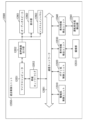
- First Embodiment Fig. 1 is a block diagram showing a schematic configuration of a calculation device according to a first embodiment.
- the calculation device 1 shown in Fig. 1 includes a plurality of pixels 10, a signal processing circuit 20, a calculator 30, signal input/output units 40 and 50, a drive circuit 60, and a digital to analog (DA) converter 70.
- DA digital to analog
- the multiple pixels 10 are arranged in a two-dimensional array, in other words in a matrix.
- the shape of this pixel array may be a square in which the number of pixels in the row direction is the same as the number of pixels in the column direction, or a rectangle in which the number of pixels in the row direction is different from the number of pixels in the column direction.
- Each pixel 10 includes a signal detector 11, a signal input selection unit 12, an AD (Analog to Digital) converter 13, a signal memory selection unit 14, and multiple memory units 15.
- the signal detector 11 outputs a first analog signal indicating the detection result of the physical signal.
- the physical signal is, for example, an optical signal.
- the first analog signal is a pixel signal SIG1 obtained by photoelectrically converting the optical signal.
- the signal input selection unit 12 selects the pixel signal SIG1 or a second analog signal indicating the calculation result of the calculator 30 as an input signal to the AD converter 13.
- the second analog signal is, for example, the calculation signal SIG2 indicating the calculation result of the calculator 30.
- the AD converter 13 digitally converts the pixel signal SIG1 and the calculation signal SIG2.
- an AD converter 13 is provided for each pixel 10.
- an AD converter 13 may be provided for each pixel column or for each pixel row.
- an AD converter 13 may be provided for each pixel array.
- the signal storage selection unit 14 selects from among multiple storage units 15 the storage destination for the digital signal VCO generated by the AD converter 13.
- Each memory unit 15 stores a digital code supplied from the signal input/output unit 40, which is determined by the transition timing of the digital signal VCO selected by the signal storage selection unit 14. In this embodiment, there are two memory units 15, but there may be three or more. Each memory unit 15 may store different types of signals, such as the pixel signal SIG1 of the pixel 10 and the calculation signal SIG2 of the calculator 30. In addition, a memory unit 15 that is read out by the signal input/output unit 40 and is no longer needed may be overwritten. Furthermore, multiple adjacent memory units 15 may share and store a single signal.
- the signal processing circuit 20 performs predetermined signal processing, such as CDS (Correlated Double Sampling) processing, on the digital signal VCO generated by the AD converter 13.
- CDS Correlated Double Sampling
- the calculator 30 performs an analog multiply-and-accumulate operation on the digital signal VCO generated by the AD converter 13, and outputs the operation result as a calculation signal SIG2.
- the signal input/output unit 40 is provided between the pixel 10 and the signal processing circuit 20.
- the signal input/output unit 40 reads out the digital signal determined by the digital signal VCO from the memory unit 15 of each pixel 10 and outputs it to the signal processing circuit 20.
- the signal input/output unit 50 is provided between the calculator 30 and the pixel 10.
- the signal input/output unit 50 outputs the calculation signal SIG2 input from the calculator 30 to the pixel 10.
- the drive circuit 60 drives the calculation device 1.
- the DAC 70 generates a reference signal REF and outputs it to AD converter 13.
- the reference signal REF is a slope signal whose voltage level decreases over time at a predetermined gradient.
- FIG. 2 is a circuit diagram showing an example of the configuration of a pixel 10 according to the first embodiment.
- the signal detector 11 includes a photoelectric conversion element 111, a discharge transistor 112, a transfer transistor 113, a reset transistor 114, a capacitance element 115, and a floating diffusion layer (FD) 116.
- FD floating diffusion layer
- the photoelectric conversion element 111 is, for example, a photodiode (PD).
- the anode of the photoelectric conversion element 111 is grounded to an appropriate potential.
- the cathode of the photoelectric conversion element 111 is connected to the discharge transistor 112 and the transfer transistor 113.
- the photoelectric conversion element 111 photoelectrically converts the incident optical signal.
- the discharge transistor 112 turns on and off depending on the level of a discharge signal OFG input to its gate from the drive circuit 60.
- the discharge transistor 112 is used when adjusting the exposure period. Specifically, when the drive circuit 60 turns on the discharge transistor 112 to start the exposure period at a desired timing, the charge that had been accumulated in the photoelectric conversion element 111 up to that point is discharged. As a result, the exposure period begins after the discharge transistor 112 is turned off.
- the transfer transistor 113 is turned on and off depending on the level of the transfer signal TX input to its gate from the drive circuit 60. When the transfer transistor 113 is turned on, the charge generated in the photoelectric conversion element 111 is transferred to the floating diffusion layer 116.
- the reset transistor 114 turns on and off depending on the level of a reset signal RST input to its gate from the drive circuit 60.
- the reset transistor 114 together with the capacitance element 115, resets the charge held in the floating diffusion layer 116.
- the source of the reset transistor 114 is connected to the capacitance element 115.
- the drain of the reset transistor 114 is connected to the drain of the transistor 134.
- the transistor 134 is turned on and off according to the level of the initialization signal xPINI input to its gate from the drive circuit 60.
- the reset transistor 114 and the transistor are turned on, the potential of the floating diffusion layer 116 is reset to the initialization potential via the power supply voltage VDDH.
- the floating diffusion layer 116 generates a pixel signal SIG1 according to the amount of charge transferred from the photoelectric conversion element 111. This converts the optical signal incident on the photoelectric conversion element 111 into the pixel signal SIG1.
- the signal input selection unit 12 is connected between the transfer transistor 113 and the reset transistor 114.
- the signal input selection unit 12 is composed of, for example, an n-channel MOS transistor.
- a drive signal FDG is input from the drive circuit 60 to the gate of the signal input selection unit 12.
- the signal input selection unit 12 turns on and off depending on the level of the drive signal FDG.
- the calculation signal SIG2 is input to the gate of the comparison transistor 131 via the signal input selection unit 12.
- the pixel signal SIG1 is input to the gate of the comparison transistor 131. In this way, the signal input to the gate of the comparison transistor 131 is selected as the calculation signal SIG2 or the pixel signal SIG1 by the switching operation of the signal input selection unit 12.
- the AD converter 13 has a comparison transistor 131, capacitance elements 132 and 136, transistors 133 to 135, transistor 137, and a positive feedback circuit 138.
- the comparison transistor 131 and transistor 137 are configured as n-channel MOS transistors.
- transistors 133 to 135 are configured as p-channel MOS transistors.
- the comparison transistor 131, capacitance elements 132 and 136, and transistors 133 to 135 form a differential input circuit.
- the comparison transistor 131 functions as a comparator that compares the voltage level of the pixel signal SIG1 generated in the floating diffusion layer 116 with the voltage level of the reference signal REF generated in the DAC 70. Specifically, the gate and source of the comparison transistor 131 correspond to the input terminals of the comparator, and the drain corresponds to the output terminal.
- Transistor 133 is connected between transistor 134 and capacitance element 132. Transistor 133 turns on and off depending on the level of initialization signal xPINI2 input to its gate from drive circuit 60. When transistor 133 turns on, the source potential of comparison transistor 131, i.e., the potential of one input terminal of the comparator, is reset to power supply voltage VDDH.
- Transistor 134 is connected in series with comparison transistor 131. As described above, transistor 134 initializes floating diffusion layer 116 based on the initialization signal xPINI input to its gate from drive circuit 60.
- Transistor 135 outputs a signal indicating the result of the comparison between pixel signal SIG1 and reference signal REF in comparison transistor 131.
- the gate voltage of transistor 135 becomes lower. This turns transistor 135 on.
- One end of the capacitance element 136 is connected to the sources of the transistors 134 and 135.
- the other end of the capacitance element 136 is connected to the drain of the transistor 134 and the gate of the transistor 135.
- the capacitance element 136 accumulates charge in an electrically floating state.
- the drain of transistor 137 is connected to the drain of transistor 135.
- the source of transistor 137 is connected to positive feedback circuit 138.
- a power supply voltage VDDL is applied to the gate of transistor 137.
- the power supply voltage VDDL is lower than the power supply voltage.
- Transistor 137 converts the output signal of transistor 135 into a low-voltage signal that allows positive feedback circuit 138 to operate, and supplies the signal to positive feedback circuit 138.
- the positive feedback circuit 138 is a circuit that operates on the power supply voltage VDDL. Based on the signal supplied from the transistor 137, the positive feedback circuit 138 outputs, as a digital signal VCO, a comparison result signal that is inverted when the pixel signal SIG1 is higher than the reference signal REF.
- the positive feedback circuit 138 has transistors 138a to 138g.
- transistors 138a, 138b, 138d, and 138e are configured as p-channel MOS transistors.
- Transistors 138c, 138f, and 138g are configured as n-channel MOS transistors.
- Transistors 138d to 138g form a NOR circuit.
- the source of transistor 137 is connected to the drains of transistors 138b and 138c and the gates of transistors 138d and 138f.
- the sources of transistors 138a and 138d are connected to the power supply voltage VDDL.
- the drain of transistor 138a is connected to the source of transistor 138b.
- the gate of transistor 138b is connected to the drains of transistors 138e, 138f and 138g, which are also the output terminal of the positive feedback circuit 138.
- the sources of transistors 138c, 138f and 138g are grounded.
- the gates of transistors 138a and 138c receive initialization signals INI2 and INI1, respectively, from the drive circuit 60.
- the gates of transistors 138e and 138g receive the FORCE signal, respectively, from the drive circuit 60.
- connection point between the drains of transistors 138e, 138f, and 138g is the output terminal from which the AD converter 13 outputs the digital signal VCO.
- the signal storage selection unit 14 has a signal control unit 141 and a signal control unit 142.
- the signal control unit 141 and the signal control unit 142 are configured with a multiplexer.
- a digital signal VCO generated by the AD converter 13 is input to one input terminal of the signal control unit 141 and the signal control unit 142.
- a WORD P signal and a WORD D signal are input to the other input terminal of the signal control unit 141 and the signal control unit 142.
- the outputs of the signal control units 141 and 142 are connected to the storage unit 15.
- the signal control unit 141 controls the operation of writing the digital code supplied from the signal input/output unit 40, which is determined by the digital signal VCO output from the AD converter 13 during the reset period (P phase period) when the transfer transistor 113 is off before exposure, to the first storage unit 151 connected to the signal control unit 141 among the multiple storage units 15.
- the signal control unit 142 controls the operation of writing the digital code supplied from the signal input/output unit 40, which is determined by the digital signal VCO obtained by digitally converting the pixel signal SIG1 by the AD converter 13, to the second storage unit 152 connected to the signal control unit 142 among the multiple storage units 15, during the data transfer period (D phase period) when the transfer transistor 113 is on after exposure.
- the signal control unit 141 or the signal control unit 142 controls the operation of writing the digital code supplied from the signal input/output unit 40, which is determined by the digital signal VCO obtained by digitally converting the calculation signal SIG2 by the AD converter 13, to the first storage unit 151 or the second storage unit 152 during the period when the signal input selection unit 12 is on.
- the first memory unit 151 and the second memory unit 152 are composed of latch circuits. Furthermore, the latch circuits of the first memory unit 151 and the second memory unit 152 are provided with switches Ta and Tb, respectively. When the switches Ta and Tb are turned on, the digital signal VCO data is written to the first memory unit 151 and the second memory unit 152. Thereafter, when the switches Ta and Tb are turned off, the data stored in the first memory unit 151 and the second memory unit 152 is finalized.
- the signal input/output unit 40 has a repeater 401 and a repeater 402.
- the repeater 401 and the repeater 402 perform operations to write data to the first memory unit 151 and the second memory unit 152 based on the control of the signal control units 141 and 142.
- the repeater 401 and the repeater 402 also perform operations to read data from the first memory unit 151 and the second memory unit 152 based on the control of the signal control units 141 and 142.
- Repeater 401 and repeater 402 are supplied with a digital time code from digital code generation unit 403.
- the data output from each storage unit to each repeater is output to signal processing circuit 20.
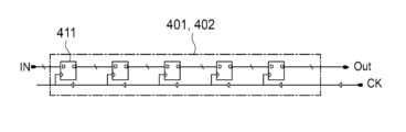
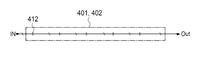
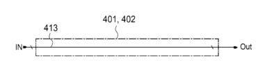
- FIGS. 3A to 3C are diagrams showing the configuration of repeaters 401 and 402.
- Repeaters 401 and 402 shown in FIG. 3A are composed of multiple flip-flops 411.
- a control clock signal CK is input to each flip-flop 411.
- Repeaters 401 and 402 may be configured to have the same control timing for flip-flops 411, such as a clock tree, with respect to the control clock signal CK, but this configuration is expected to require large area and power. For this reason, it is desirable for the input direction of the control clock signal CK in repeaters 401 and 402 to be opposite to the signal output direction of flip-flops 411.
- the repeaters 401 and 402 shown in FIG. 3B are composed of multiple tri-state inverters 412. In this case, a control signal for realizing a tri-state output is input from the drive circuit 60 to each tri-state inverter 412.
- the repeaters 401 and 402 shown in FIG. 3C are configured with metal wiring 413 that transmits the digital signal VCO.
- the configuration of the repeaters 401 and 402 can be simplified compared to FIG. 3A and FIG. 3B.
- each repeater outputs the calculation signal SIG2 output from the calculator 30 to the corresponding signal input selection unit 12.
- the calculator 30 shown in FIG. 4A has a plurality of memory cells 301, a plurality of current sources 302, and a read circuit 303.
- the plurality of memory cells 301 are arranged in a two-dimensional array.
- a resistive random access memory (ReRAM), a phase change memory (PCM), a magnetoresistive random memory (MRAM), or a ferroelectric random access memory (FeRAM) can be applied to each memory cell 301.
- the memory cells 301 may also be static random access memory (SRAM) or a non-volatile memory.
- SRAM static random access memory
- Each memory cell 301 holds weight coefficients W1 to Wn.
- the multiple current sources 302 are composed of, for example, MOS transistors.
- the multiple current sources 302 are individually connected to the multiple memory cells 301.
- the read circuit 303 is composed of an AD converter 304.
- the input signals x1 to xn input from the signal processing circuit 20 are multiplied by the weighting coefficients W1 to Wn of the memory cells 301.
- the multiplied values are converted to current values in the current sources 302.
- the current values of the current sources 302 are added together and input to the read circuit 303.
- the AD converter 304 converts the added current values into analog. This generates the calculation signal SIG2.
- the calculator 30 shown in FIG. 4B differs from the calculator 30 shown in FIG. 4A in that it has multiple capacitive elements 305 instead of multiple current sources 302.
- Each capacitive element 305 holds a charge indicating the multiplication result of input signals x1 to xn and weighting coefficients W1 to Wn.
- the charges held in each capacitive element 305 are added together and input to the read circuit 303.
- an AD converter 304 converts the added charges into analog form. This generates a calculation signal SIG2.
- the calculator 30 shown in FIG. 4B is an analog neural network circuit that enables product-sum calculations using electric charge by changing the capacitance value of the capacitive element 305. This calculator 30 is not affected by settling variations by ensuring the signal settling time, and since the capacitance value is relatively less likely to vary than the resistance value, the calculation accuracy is higher than that of a resistor.
- the calculator 30 shown in FIG. 4C differs from the calculator 30 shown in FIG. 4A in that it has multiple inverter elements 306 instead of multiple current sources 302, and in the configuration of the read circuit 303.
- the read circuit 303 has a capacitance element 307 and switches 308 and 309.
- Switch 309 is connected in series to inverter element 306.
- Switch 308 and capacitive element 307 are connected in parallel to switch 309.
- Switch 308 and switch 309 are configured, for example, as MOS transistors that are driven and controlled by drive circuit 60.
- the multiplied values of the input signals x1 to xn and the weighting coefficients W1 to Wn are input to each inverter element 306.
- the multiplied values are added by each inverter element 306 and input to the read circuit 303.
- the read circuit 303 the sum is converted to a voltage through a time calculation, and this voltage value corresponds to the calculation signal SIG2.
- the time calculation is performed by the delay of the inverter element 306, and the time for charging the capacitance element 307 can be made variable by the switches 308 and 309 according to the amount of delay.
- the calculator 30 shown in FIG. 4D differs from the calculator 30 shown in FIG. 4A in that it has multiple capacitive elements 305 instead of multiple current sources 302, and in the configuration of the read circuit 303.
- the read circuit 303 is composed of an integrator. Specifically, the read circuit 303 has a capacitive element 307, a switch 308, and an operational amplifier 310.
- Switch 308 and capacitive element 307 are connected in parallel between the inverting input terminal (-) and the output terminal of operational amplifier 310.
- a predetermined voltage is applied to the non-inverting input terminal (+) of operational amplifier 310.
- the charge is read out by feedback to capacitive element 307, which is a feedback capacitance connected between the input and output terminals of operational amplifier 310.
- each capacitance element 305 holds a charge indicating the multiplication result of the input signals x1 to xn and the weighting coefficients W1 to Wn.
- the charges held in each capacitance element 305 are added together and input to the read circuit 303.
- a calculation signal SIG2 is output from the output terminal of the operational amplifier 310.
- the weighting coefficient of each capacitive element 305 may be set at a power of 2 ratio. Alternatively, the weighting coefficient of each capacitive element 305 may be set at a logarithmic ratio. Alternatively, the weighting coefficient of each capacitive element 305 may be set at a linear ratio.
- the input signal of the calculator 30 is a digital signal supplied from the outside through the signal input/output unit 40, and in particular, the digital signal VCO indicates the acquisition timing. In FIG.
- the capacitance value (size) C of the capacitive element 305 changes depending on the weighting coefficient w.
- the amount of signal stored in this capacitance value C changes depending on the weighting coefficient w.
- the logarithms increase the set values of the capacitance value C logarithmically, for example, 0.3, 0.47, 0.6, 0.69, etc.
- Each of these logarithms corresponds to a digital code of, for example, 2, 3, 4, 5.
- the set values of the capacitance values C have a linear relationship with the weighting coefficients w.
- the capacitance values C are set to 1, 2, 3, 4, 5...
- the corresponding weighting coefficients w for each capacitance value C are also 1, 2, 3, 4, 5....
- FIG. 5 is a diagram showing an example of the structure of the computing device 1 according to the first embodiment.
- the computing device 1 has a layered structure in which a first substrate 101 and a second substrate 102 are layered.
- the first substrate 101 and the second substrate 102 are, for example, silicon substrates.
- the first substrate 101 and the second substrate 102 are electrically connected by, for example, a so-called Cu-Cu bond that bonds connection terminals together.
- the bonding method for the first substrate 101 and the second substrate 102 may also be a TSV (Through Silicon Via) bond using a through electrode, a microbump bond, or a magnetic coupling.
- TSV Thinit Silicon Via
- the pixel array 110 is disposed on the first substrate 101.
- a plurality of pixels 10 are arranged in a two-dimensional array.
- the signal processing circuit 20, the calculator 30, the signal input/output units 40 and 50, and the drive circuit 60 are disposed on the second substrate 102.
- the first substrate 101 may further be composed of two laminated substrates.
- the photoelectric conversion element 111 of the signal detector 11 may be disposed on one laminated substrate, and the remaining circuit elements may be disposed on the other laminated substrate. In this way, by distributing the circuit elements of the signal detector 11 across multiple substrates, a sufficient light receiving area for the optical signal can be secured.
- FIG. 6 is a flowchart showing the operation procedure of the calculation device 1 according to the first embodiment. The operation of the calculation device 1 according to the first embodiment will be described below with reference to FIG. 6. Note that the operation after the start of exposure will be described here.
- step S11 exposure is first started (step S11).
- step S11 the photoelectric conversion element 111 of each pixel 10 performs photoelectric conversion of the optical signal.
- the initial state of the circuit is set as the circuit reset level, and A/D conversion is performed through the signal input selection unit 12, A/D converter 13, signal memory selection unit 14, and memory unit 15.
- the signal input selection unit 12 performs an operation to select a signal to be input to the A/D converter 13 (step S12).
- the pixel signal generated in step S11 is input to the A/D converter 13.
- step S11 of this embodiment a global shutter operation is performed in which all pixels 10 simultaneously detect a light signal.
- the AD converter 13 AD converts the input signal, here the pixel signal SIG1 (step S13).
- the AD converter 13 converts the pixel signal SIG1 into a digital signal supplied from the signal input/output unit 40 determined by the digital signal VCO.
- This digital signal is stored in the memory unit 15 stored by the signal storage selection unit 14.
- the digital signal is then read out from the memory unit 15 by the signal input/output unit 40 and input to the signal processing circuit 20.
- the signal processing circuit 20 performs a predetermined signal processing on the digital signal. This includes, for example, correlated double sampling, which takes the difference between a reset level and a signal level.
- the result is the pixel signal SIG1.
- the processed digital signal is then input to the calculator 30.
- step S14 the calculator 30 performs a product-sum operation on the digital signal (step S14).
- step S14 the calculator 30 performs a product-sum operation to generate a calculation signal SIG2.
- the generated calculation signal SIG2 is input to the AD converter 13 of each pixel 10 by the signal input/output unit 50.
- the calculator 30 is set to perform the multiply-and-accumulate operation multiple times. Therefore, the calculation process does not end until the number of multiply-and-accumulate operations reaches a preset number (step S15). If the calculation process does not end (step S15: No), the operations of steps S12 to S15 are repeated. In this case, in step S12, the signal input selection unit 12 selects the calculation signal SIG2 as an input signal to the AD converter 13. Therefore, the signal input selection unit 12, which is made up of a MOS transistor, is turned on. As a result, the calculation signal SIG2 generated in step S14 is input to the AD converter 13 via the signal input selection unit 12.
- step S15 When the calculation process is completed (step S15: YES), the calculation signal SIG2 is output from the output unit 80 to the outside (step S16). This ends the operation of the calculation device 1.
- the digital signal input to the calculator 30 is output as an analog calculation signal SIG2.
- This calculation signal SIG2 is also fed back to the signal input selection unit 12 connected to the input terminal of the AD converter 13. This allows the calculation loop of the calculator 30 to be realized using the shortest data transmission path. As a result, high power efficiency can be achieved, making it possible to suppress power consumption.
- Second Embodiment A second embodiment of the present disclosure will be described.
- components similar to those in the first embodiment are denoted by the same reference numerals, detailed description will be omitted, and differences from the first embodiment will be mainly described.
- FIG. 7 is a diagram showing an example of the structure of a calculation device according to the second embodiment.
- the calculation device 2 shown in FIG. 7 has a first pixel array 110a and a second pixel array 110b.
- the first pixel array 110a and the second pixel array 110b are arranged apart from each other on the first substrate 101. That is, a space is formed between the first pixel array 110a and the second pixel array 110b.
- the shape of the first pixel array 110a and the shape of the second pixel array 110b may be the same, that is, both square or rectangular, or one may be square and the other rectangular.
- each first pixel 10a is an effective pixel having a signal detector 11, a signal input selection section 12, an AD converter 13, a signal storage selection section 14, and a storage section 15, similar to the pixel 10 described in the first embodiment. Therefore, in each first pixel 10a, the optical signal 200 is photoelectrically converted into a pixel signal SIG1 by the signal detector 11. Furthermore, the pixel signal SIG1 is AD-converted into a digital signal by the AD converter 13, and after CDS processing etc. through the signal processing circuit 20, becomes an AD-converted signal of the pixel signal SIG1.
- the second pixel array 110b has a plurality of second pixels 10b arranged in a two-dimensional array.
- each second pixel 10b has a signal detector 11, a signal input selection section 12, an AD converter 13, a signal storage selection section 14, and a storage section 15.
- each second pixel 10b is an OPB (Optical Black) pixel that detects the black level. Therefore, the photoelectric conversion element 111 of the second pixel 10b is shielded from light by a light-shielding film.
- OPB Optical Black
- the calculation signal SIG2 of the calculator 30 is input to the second pixel 10b.
- the MOS transistor constituting the signal input selection unit 12 of the second pixel 10b is turned on. Therefore, the calculation signal SIG2 is AD converted to a digital signal VCO by the AD converter 13 of the second pixel 10b.
- the AD converter 13 that performs AD conversion on the pixel signal SIG1 and the AD converter 13 that performs AD conversion on the calculation signal SIG2 are physically separated within the first substrate 101.
- two AD converters 13 that perform different AD conversions are arranged in different areas (pixel arrays).
- the calculation loop of the calculator 30 is repeated between the first substrate 101 and the second substrate 102. Therefore, in this embodiment as well, the calculation loop of the calculator 30 can be realized using the shortest data transmission path, making it possible to suppress power consumption.
- pixel signal SIG1 when pixel signal SIG1 is selected in the signal selection process (step S12), only the AD converter 13 of the first pixel 10a performs AD conversion processing to generate a digital signal in the AD conversion process (step S13).
- calculation signal SIG2 is selected in the signal selection process (step S12)
- only the AD converter 13 of the second pixel 10b performs AD conversion processing to generate a digital signal in the AD conversion process (step S13).
- the AD conversion process may be performed on both the first pixel 10a and the second pixel 10b.
- the signal input/output unit 40 inputs only the digital signal generated by the first pixel 10a to the signal processing circuit 20. This digital signal is then processed by the signal processing circuit 20 and input to the calculator 30.
- the calculation signal SIG2 is selected in the signal selection process (step S12)
- the signal input/output unit 40 inputs only the digital signal generated by the second pixel 10b to the signal processing circuit 20. This digital signal is then processed by the signal processing circuit 20 and input to the calculator 30.
- the ROI Region Of Interest
- FIG. 8 is a diagram showing an example of the structure of a calculation device according to a first modified example of the second embodiment.
- the first pixel array 110a and the second pixel array 110b are arranged adjacent to each other on the first substrate 101. Even with this layout, the AD converter 13 of the first pixel 10a and the AD converter 13 of the second pixel 10b are physically separated.
- the calculation loop of the calculator 30 is repeated between the first substrate 101 and the second substrate 102. Therefore, in this modified example as well, the calculation loop of the calculator 30 can be realized using the shortest data transmission path, making it possible to reduce power consumption.
- FIG. 9 is a diagram showing an example of the structure of a calculation device according to a second modified example of the second embodiment.
- the calculation device 2b according to the first modified example further includes a third pixel array 110c in addition to the first pixel array 110a and the second pixel array 110b.
- the third pixel array 110c is disposed on the first substrate 101 together with the first pixel array 110a and the second pixel array 110b.
- the third pixel array 110c has the third pixels 10c arranged in a two-dimensional array.
- the calculation signal SIG2 of the calculator 30 is input to the third pixel 10c.
- the AD converter 13 of the third pixel 10c performs AD conversion only on the calculation signal SIG2. That is, in the calculation device 2b of this modified example, the pixel signal SIG1 is AD converted only by the AD converter 13 of the first pixel 10a, and the calculation signal SIG2 is AD converted only by the AD converter 13 of the third pixel 10c.
- the signal input selection unit 12 is not required in the third pixel 10c. This makes it possible to simplify the circuit configuration of the third pixel 10c.
- the DAC 70 outputs the same reference signal REF to the AD converter 13, specifically to the source of the comparison transistor 131.
- the DAC 70 outputs a different reference signal depending on the target of AD conversion.
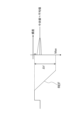
- FIG. 10 is a diagram showing an example waveform of a reference signal according to the third embodiment.
- the horizontal axis indicates time, and the vertical axis indicates the voltage of the reference signal.
- the DAC 70 when the AD converter 13 AD converts the pixel signal SIG1, the DAC 70 outputs a first reference signal REF1 to the source of the comparison transistor 131.
- the AD converter 13 AD converts the calculation signal SIG2
- the DAC 70 outputs a second reference signal REF2 to the source of the comparison transistor 131.
- the slope of the first reference signal REF1 is different from the slope of the second reference signal REF2.
- the slope of the first reference signal REF1 is greater than the slope of the second reference signal REF2, but the relationship between the magnitudes of the slopes may be reversed.
- DAC 70 outputs two types of reference signals with different slopes, but it may output three or more types of reference signals.
- DAC 70 may output, for example, a reference signal with a different slope for each region in the pixel array 110.
- DAC 70 may output, for example, a reference signal with a different slope for the first AD conversion and the second AD conversion.
- the DAC 70 outputs multiple types of reference signals with different slopes, making it possible to set a specific weighting for the calculation signal SIG2.
- the digital signals are read out by the signal input/output unit 40 in the order of pixel rows and pixel columns and input to the calculator 30, and the calculation signal SIG2 is input by the signal input/output unit 50 to the AD converter 13 of the same pixel 10 as the corresponding pixel signal SIG1.
- the signal input/output unit 40 may input the digital signal to the calculator 30 by swapping the pixel columns and pixel rows of the pixel array 110, or the signal input/output unit 50 may input the calculation signal SIG2 to the AD converter 13 by swapping the pixel columns and pixel rows. This makes it possible to perform a transposition calculation on the calculation signal SIG2.
- the pixel signal SIG1 is input first to the AD converter 13 of each pixel 10. Therefore, in the first and second embodiments described above, the reference signal REF input from the DAC 70 to the AD converter 13 is optimized based on the pixel signal SIG1. However, this reference signal REF is not necessarily optimal for the calculation signal SIG2 as well.
- the AD converter 13 performs a process of optimizing the reference signal REF according to the result of AD conversion of the calculation signal SIG2.
- the optimization process of the reference signal REF is described below.
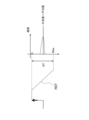
- FIG. 11 is a diagram showing an example of the results of the initial AD conversion process of the calculation signal SIG2 by the AD converter 13.
- a distribution showing the comparison result between the calculation signal SIG2 of each pixel 10 and the reference signal REF is shown in correspondence with the waveform of the reference signal REF. This distribution is created by, for example, the signal processing circuit 20.
- the median (average value) of the voltage distribution of the calculation signal SIG2 when it exceeds the reference signal REF is biased towards the ends of the voltage range ⁇ V of the reference signal REF.
- the signal processing circuit 20 calculates the maximum value Max and minimum value Min of the voltage of the calculation signal SIG2 when it exceeds the reference signal REF.
- the DAC 70 optimizes the reference signal REF so that the median value (Max+Min)/2 of the above voltages is in the center of the voltage range ⁇ V.
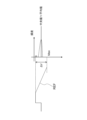
- FIG. 12 is a diagram showing an example of the waveform of the reference signal REF optimized according to the voltage distribution of the calculation signal SIG2.
- the reference signal REF shown in FIG. 12 has a higher slope start offset voltage than the reference signal REF shown in FIG. 11. This causes the median (average value) of the voltage distribution of the calculation signal SIG2 to move to the center of the voltage range ⁇ V of the reference signal REF.
- FIG. 13 is a diagram showing another example of the waveform of the reference signal REF optimized according to the voltage distribution of the calculation signal SIG2.
- the reference signal REF shown in FIG. 13 has a smaller slope than the reference signal REF shown in FIG. 12.
- the median (average value) of the voltage distribution of the calculation signal SIG2 moves to the center of the voltage range ⁇ V of the reference signal REF.
- both the method shown in FIG. 12 and the method shown in FIG. 13 may be used as a method for optimizing the reference signal REF. In this case, it is possible to further optimize the reference signal REF.
- the technology according to the present disclosure can be applied to various products.
- the technology according to the present disclosure may be realized as a device mounted on any type of moving body such as an automobile, an electric vehicle, a hybrid electric vehicle, a motorcycle, a bicycle, a personal mobility device, an airplane, a drone, a ship, or a robot.
- FIG. 14 is a block diagram showing a schematic configuration example of a vehicle control system, which is an example of a mobile object control system to which the technology disclosed herein can be applied.
- the vehicle control system 12000 includes a plurality of electronic control units connected via a communication network 12001.
- the vehicle control system 12000 includes a drive system control unit 12010, a body system control unit 12020, an outside vehicle information detection unit 12030, an inside vehicle information detection unit 12040, and an integrated control unit 12050.
- a microcomputer 12051 Also shown in the figure are a microcomputer 12051, an audio/video output unit 12052, and an in-vehicle network I/F (Interface) 12053 as functional configurations of the integrated control unit 12050.
- the drive system control unit 12010 controls the operation of devices related to the drive system of the vehicle according to various programs.
- the drive system control unit 12010 functions as a control device for a drive force generating device for generating the drive force of the vehicle, such as an internal combustion engine or a drive motor, a drive force transmission mechanism for transmitting the drive force to the wheels, a steering mechanism for adjusting the steering angle of the vehicle, and a braking device for generating a braking force for the vehicle.
- the body system control unit 12020 controls the operation of various devices installed in the vehicle body according to various programs.
- the body system control unit 12020 functions as a control device for a keyless entry system, a smart key system, a power window device, or various lamps such as headlamps, tail lamps, brake lamps, turn signals, and fog lamps.
- radio waves or signals from various switches transmitted from a portable device that replaces a key can be input to the body system control unit 12020.
- the body system control unit 12020 accepts the input of these radio waves or signals and controls the vehicle's door lock device, power window device, lamps, etc.
- the outside-vehicle information detection unit 12030 detects information outside the vehicle equipped with the vehicle control system 12000.
- the image capturing unit 12031 is connected to the outside-vehicle information detection unit 12030.
- the outside-vehicle information detection unit 12030 causes the image capturing unit 12031 to capture images outside the vehicle and receives the captured images.
- the outside-vehicle information detection unit 12030 may perform object detection processing or distance detection processing for people, cars, obstacles, signs, or characters on the road surface based on the received images.
- the imaging unit 12031 is an optical sensor that receives light and outputs an electrical signal according to the amount of light received.
- the imaging unit 12031 can output the electrical signal as an image, or as distance measurement information.
- the light received by the imaging unit 12031 may be visible light, or may be invisible light such as infrared light.
- the in-vehicle information detection unit 12040 detects information inside the vehicle.
- a driver state detection unit 12041 that detects the state of the driver is connected.
- the driver state detection unit 12041 includes, for example, a camera that captures an image of the driver, and the in-vehicle information detection unit 12040 may calculate the driver's degree of fatigue or concentration based on the detection information input from the driver state detection unit 12041, or may determine whether the driver is dozing off.
- the microcomputer 12051 can calculate control target values for the driving force generating device, steering mechanism, or braking device based on information inside and outside the vehicle acquired by the outside vehicle information detection unit 12030 or the inside vehicle information detection unit 12040, and output control commands to the drive system control unit 12010.
- the microcomputer 12051 can perform cooperative control aimed at realizing the functions of an ADAS (ADvanced Driver Assistance System), including vehicle collision avoidance or impact mitigation, following driving based on the distance between vehicles, maintaining vehicle speed, vehicle collision warning, or vehicle lane departure warning.
- ADAS Advanced Driver Assistance System
- the microcomputer 12051 can also perform cooperative control for the purpose of autonomous driving, which allows the vehicle to travel autonomously without relying on the driver's operation, by controlling the driving force generating device, steering mechanism, braking device, etc. based on information about the surroundings of the vehicle acquired by the outside vehicle information detection unit 12030 or the inside vehicle information detection unit 12040.
- the microcomputer 12051 can also output control commands to the body system control unit 12030 based on information outside the vehicle acquired by the outside information detection unit 12030. For example, the microcomputer 12051 can control the headlamps according to the position of a preceding vehicle or an oncoming vehicle detected by the outside information detection unit 12030, and perform cooperative control aimed at preventing glare, such as switching from high beams to low beams.
- the audio/image output unit 12052 transmits at least one output signal of audio and image to an output device capable of visually or audibly notifying the occupants of the vehicle or the outside of the vehicle of information.
- an audio speaker 12061, a display unit 12062, and an instrument panel 12063 are exemplified as output devices.
- the display unit 12062 may include, for example, at least one of an on-board display and a head-up display.
- FIG. 15 shows an example of the installation position of the imaging unit 12031.
- the imaging unit 12031 includes imaging units 12101, 12102, 12103, 12104, and 12105.
- the imaging units 12101, 12102, 12103, 12104, and 12105 are provided, for example, at the front nose, side mirrors, rear bumper, back door, and upper part of the windshield inside the vehicle cabin of the vehicle 12100.
- the imaging unit 12101 provided at the front nose and the imaging unit 12105 provided at the upper part of the windshield inside the vehicle cabin mainly acquire images of the front of the vehicle 12100.
- the imaging units 12102 and 12103 provided at the side mirrors mainly acquire images of the sides of the vehicle 12100.
- the imaging unit 12104 provided at the rear bumper or back door mainly acquires images of the rear of the vehicle 12100.
- the imaging unit 12105 provided at the upper part of the windshield inside the vehicle cabin is mainly used to detect leading vehicles, pedestrians, obstacles, traffic lights, traffic signs, lanes, etc.
- FIG. 15 shows an example of the imaging ranges of the imaging units 12101 to 12104.
- Imaging range 12111 indicates the imaging range of the imaging unit 12101 provided on the front nose
- imaging ranges 1211212113 indicate the imaging ranges of the imaging units 12102 and 12103 provided on the side mirrors
- imaging range 12114 indicates the imaging range of the imaging unit 12104 provided on the rear bumper or back door.
- an overhead image of the vehicle 12100 viewed from above is obtained by superimposing the image data captured by the imaging units 12101 to 12104.
- At least one of the imaging units 12101 to 12104 may have a function of acquiring distance information.
- at least one of the imaging units 12101 to 12104 may be a stereo camera consisting of multiple imaging elements, or an imaging element having pixels for phase difference detection.
- the microcomputer 12051 can obtain the distance to each solid object within the imaging ranges 12111 to 12114 and the change in this distance over time (relative speed with respect to the vehicle 12100) based on the distance information obtained from the imaging units 12101 to 12104, and can extract as a preceding vehicle, in particular, the closest solid object on the path of the vehicle 12100 that is traveling in approximately the same direction as the vehicle 12100 at a predetermined speed (e.g., 0 km/h or faster). Furthermore, the microcomputer 12051 can set the inter-vehicle distance that should be maintained in advance in front of the preceding vehicle, and perform automatic braking control (including follow-up stop control) and automatic acceleration control (including follow-up start control). In this way, cooperative control can be performed for the purpose of automatic driving, which runs autonomously without relying on the driver's operation.
- automatic braking control including follow-up stop control
- automatic acceleration control including follow-up start control
- the microcomputer 12051 classifies and extracts three-dimensional object data on three-dimensional objects, such as two-wheeled vehicles, ordinary vehicles, large vehicles, pedestrians, utility poles, and other three-dimensional objects, based on the distance information obtained from the imaging units 12101 to 12104, and can use the data to automatically avoid obstacles.
- the microcomputer 12051 distinguishes obstacles around the vehicle 12100 into obstacles that are visible to the driver of the vehicle 12100 and obstacles that are difficult to see.
- the microcomputer 12051 determines the collision risk, which indicates the risk of collision with each obstacle, and when the collision risk is equal to or exceeds a set value and there is a possibility of a collision, it can provide driving assistance for collision avoidance by outputting an alarm to the driver via the audio speaker 12061 or the display unit 12062, or by forcibly decelerating or steering to avoid a collision via the drive system control unit 12010.
- At least one of the imaging units 12101 to 12104 may be an infrared camera that detects infrared rays.
- the microcomputer 12051 can recognize a pedestrian by determining whether or not a pedestrian is present in the captured image of the imaging units 12101 to 12104. The recognition of such a pedestrian is performed, for example, by a procedure of extracting feature points in the captured image of the imaging units 12101 to 12104 as infrared cameras, and a procedure of performing pattern matching processing on a series of feature points that indicate the contour of an object to determine whether or not it is a pedestrian.
- the audio/image output unit 12052 controls the display unit 12062 to superimpose a rectangular contour line for emphasis on the recognized pedestrian.
- the audio/image output unit 12052 may also control the display unit 12062 to display an icon or the like indicating a pedestrian at a desired position.
- the technology according to the present disclosure can be applied to, for example, the imaging unit 12031.
- the arithmetic devices according to the first to third embodiments can be applied to the imaging unit 12031.
- the power consumption of the imaging unit 12031 can be reduced, making it possible to reduce the power consumption of the vehicle control system.
- the present technology can be configured as follows. (1) a signal detector that outputs a first analog signal indicative of a detection result of a physical signal; an AD converter provided downstream of the signal detector; a calculator that calculates the digital signal output from the AD converter and outputs a second analog signal indicating a calculation result, the signal detector having a floating diffusion layer for converting the physical signal into the first analog signal; The second analog signal is input to a stage preceding the AD converter that is electrically connected to the floating diffusion layer. (2) The arithmetic device according to (1), further comprising a signal input selection unit that selects the first analog signal or the second analog signal as an input signal to the AD converter.
- the arithmetic device according to (1) or (2) further comprising: (4) The arithmetic device according to any one of (1) to (3), further comprising a plurality of pixel arrays in which pixels including the signal detector and the AD converter are arranged in a two-dimensional array. (5) The arithmetic unit according to (4), wherein the pixel array has a positive shape. (6) The arithmetic unit according to (4), wherein the pixel array has a rectangular shape.
- the computing device according to any one of (1) to (6), wherein a plurality of the signal detectors simultaneously detect the physical signals.
- the arithmetic device according to any one of (4) to (6), wherein an AD converter of a pixel provided in a pixel array that is a detection target for the digital signal, among a plurality of pixel arrays, performs AD conversion on the first analog signal or the second analog signal.
- the second analog signal is input to an AD converter for a plurality of pixel rows or a plurality of pixel columns;
- the arithmetic device according to any one of (4) to (6), wherein a weighting coefficient used in the calculation of the arithmetic unit is set for each of the AD converters of the plurality of pixel rows or the plurality of pixel columns.
- the AD converter performs AD conversion on the second analog signal by comparing the second analog signal with a reference signal;
Landscapes
- Engineering & Computer Science (AREA)
- Multimedia (AREA)
- Signal Processing (AREA)
- Transforming Light Signals Into Electric Signals (AREA)
Abstract
Description
前記AD変換器と前記演算器との間で前記デジタル信号を記憶する複数の記憶部と、
前記デジタル信号の記憶先を、前記複数の記憶部から選択する信号記憶選択部と、
をさらに備えていてもよい。
前記演算器の演算に用いられる重み係数が、前記複数の画素行または前記複数の画素列のAD変換器ごとに設定されていてもよい。
前記演算装置は、前記参照信号を超えたときの前記第2アナログ信号の電圧分布を作成する信号処理回路をさらに備えていてもよい。
前記AD変換器は、前記第2アナログ信号を転置演算してもよい。
前記演算器が配置される第2基板と、をさらに備え、
前記第1基板と前記第2基板とが、互いに積層されていてもよい。
図1は、第1実施形態に係る演算装置の概略的な構成を示すブロック図である。図1に示す演算装置1は、複数の画素10と、信号処理回路20と、演算器30と、信号入出力部40、50と、駆動回路60と、DA(Digital to Analog)変換器70と、を含む。
本開示の第2実施形態について説明する。本実施形態では、第1実施形態と同様の構成要素には同じ符号を付して詳細な説明を省略し、第1実施形態と異なる点を中心に説明する。
本開示の第3実施形態について説明する。本実施形態に係る演算装置の構成は、第1実施形態に係る演算装置1または第2実施形態に係る演算装置2と同様であるため、詳細な説明を省略する。
本開示に係る技術(本技術)は、様々な製品へ応用することができる。例えば、本開示に係る技術は、自動車、電気自動車、ハイブリッド電気自動車、自動二輪車、自転車、パーソナルモビリティ、飛行機、ドローン、船舶、ロボット等のいずれかの種類の移動体に搭載される装置として実現されてもよい。
(1) 物理信号の検出結果を示す第1アナログ信号を出力する信号検出器と、
前記信号検出器の後段に設けられたAD変換器と、
前記AD変換器から出力されるデジタル信号を演算し、演算結果を示す第2アナログ信号を出力する演算器と、を備え、
前記信号検出器が、前記物理信号を前記第1アナログ信号に変換する浮遊拡散層を有し、
前記第2アナログ信号が、前記浮遊拡散層と電気的に接続された前記AD変換器の前段に入力される、演算装置。
(2) 前記第1アナログ信号または前記第2アナログ信号を前記AD変換器への入力信号として選択する信号入力選択部をさらに備える、(1)に記載の演算装置。
(3) 前記AD変換器と前記演算器との間で前記デジタル信号を記憶する複数の記憶部と、
前記デジタル信号の記憶先を、前記複数の記憶部から選択する信号記憶選択部と、
をさらに備える、(1)または(2)に記載の演算装置。
(4) 前記信号検出器と前記AD変換器とを含む画素が2次元アレイ状に配列された画素アレイを複数備える、(1)から(3)のいずれかに記載の演算装置。
(5) 前記画素アレイの形状が正方向である、(4)に記載の演算装置。
(6) 前記画素アレイの形状が長方形である、(4)に記載の演算装置。
(7) 複数の前記信号検出器が、同時に前記物理信号を検出する、(1)から(6)のいずれかに記載の演算装置。
(8) 複数の画素アレイのうち、前記デジタル信号の検出対象の画素アレイに設けられた画素のAD変換器が、前記第1アナログ信号または前記第2アナログ信号をAD変換する、(4)から(6)のいずれかに記載の演算装置。
(9) 複数の画素アレイのAD変換器が前記デジタル信号を出力した後、特定の画素アレイの前記デジタル信号が前記演算器に入力される、(4)から(6)のいずれかに記載の演算装置。
(10) 前記演算器は、前記デジタル信号を積和演算するための容量素子を有する、(1)から(9)のいずれかに記載の演算装置。
(11) 前記容量素子には、2のべき乗比に基づいて、前記積和演算の重み係数が設定されている、(10)に記載の演算装置。
(12) 前記容量素子には、対数比に基づいて前記積和演算の重み係数が設定されている、(10)に記載の演算装置。
(13) 前記容量素子には、線形比に基づいて前記積和演算の重み係数が設定されている、(10)に記載の演算装置。
(14) 前記第2アナログ信号は、複数の画素行または複数の画素列のAD変換器に入力され、
前記演算器の演算に用いられる重み係数が、前記複数の画素行または前記複数の画素列のAD変換器ごとに設定されている、(4)から(6)のいずれかに記載の演算装置。
(15) 前記AD変換器は、前記第2アナログ信号を参照信号と比較することによって、前記第2アナログ信号をAD変換し、
前記参照信号を超えたときの前記第2アナログ信号の電圧分布を作成する信号処理回路をさらに備える、(4)から(6)のいずれかに記載の演算装置。
(16) 前記参照信号の電圧範囲が、前記電圧分布に基づいて最適化される、(15)に記載の演算装置。
(17) 前記デジタル信号または前記第2アナログ信号の画素行と画素列を入れ替える信号入出力部をさらに備え、
前記AD変換器は、前記第2アナログ信号を転置演算する、(4)から(6)のいずれかに記載の演算装置。
(18) 前記AD変換器が前記第2アナログ信号をAD変換するときの重み係数が、前記第1アナログ信号をAD変換するときの重み係数から変更される、(1)から(17)のいずれかに記載の演算装置。
(19) 前記信号入出力部が、金属配線で構成される、(17)に記載の演算装置。
(20) 前記信号入出力部が、フリップフロップで構成される、(17)に記載の演算装置。
(21) 前記信号入出力部が、トライステートインバータで構成される、(17)に記載の演算装置。
(22) 前記信号検出器が配置される第1基板と、
前記演算器が配置される第2基板と、をさらに備え、
前記第1基板と前記第2基板とが、互いに積層されている、(1)から(21)のいずれかに記載の演算装置。
(23) 前記物理信号は、光信号である、(1)から(22)のいずれかに記載の演算装置。
(24) 前記信号検出器の回路素子が、複数枚の基板に分散配置されている、(1)から(23)のいずれかに記載の演算装置。
(25) 前記演算器は、アナログニューラルネットワーク回路である、請求項1から請求項24のいずれかに記載の演算装置。
10:画素
11:信号検出器
12:信号入力選択部
13:AD変換器
14:信号記憶選択部
15:記憶部
20:信号処理回路
30:演算器
40:信号入出力部
50:信号入出力部
101:第1基板
102:第2基板
110:画素アレイ
116:浮遊拡散層
305:容量素子
411:フリップフロップ
412:トライステートインバータ
413:金属配線
Claims (25)
- 物理信号の検出結果を示す第1アナログ信号を出力する信号検出器と、
前記信号検出器の後段に設けられたAD変換器と、
前記AD変換器から出力されるデジタル信号を演算し、演算結果を示す第2アナログ信号を出力する演算器と、を備え、
前記信号検出器が、前記物理信号を前記第1アナログ信号に変換する浮遊拡散層を有し、
前記第2アナログ信号が、前記浮遊拡散層と電気的に接続された前記AD変換器の前段に入力される、演算装置。 - 前記第1アナログ信号または前記第2アナログ信号を前記AD変換器への入力信号として選択する信号入力選択部をさらに備える、請求項1に記載の演算装置。
- 前記AD変換器と前記演算器との間で前記デジタル信号を記憶する複数の記憶部と、
前記デジタル信号の記憶先を、前記複数の記憶部から選択する信号記憶選択部と、
をさらに備える、請求項1に記載の演算装置。 - 前記信号検出器と前記AD変換器とを含む画素が2次元アレイ状に配列された画素アレイを複数備える、請求項1に記載の演算装置。
- 前記画素アレイの形状が正方向である、請求項4に記載の演算装置。
- 前記画素アレイの形状が長方形である、請求項4に記載の演算装置。
- 複数の前記信号検出器が、同時に前記物理信号を検出する、請求項1に記載の演算装置。
- 複数の画素アレイのうち、前記デジタル信号の検出対象の画素アレイに設けられた画素のAD変換器が、前記第1アナログ信号または前記第2アナログ信号をAD変換する、請求項4に記載の演算装置。
- 複数の画素アレイのAD変換器が前記デジタル信号を出力した後、特定の画素アレイの前記デジタル信号が前記演算器に入力される、請求項4に記載の演算装置。
- 前記演算器は、前記デジタル信号を積和演算するための容量素子を有する、請求項1に記載の演算装置。
- 前記容量素子には、2のべき乗比に基づいて、前記積和演算の重み係数が設定されている、請求項10に記載の演算装置。
- 前記容量素子には、対数比に基づいて前記積和演算の重み係数が設定されている、請求項10に記載の演算装置。
- 前記容量素子には、線形比に基づいて前記積和演算の重み係数が設定されている、請求項10に記載の演算装置。
- 前記第2アナログ信号は、複数の画素行または複数の画素列のAD変換器に入力され、
前記演算器の演算に用いられる重み係数が、前記複数の画素行または前記複数の画素列のAD変換器ごとに設定されている、請求項4に記載の演算装置。 - 前記AD変換器は、前記第2アナログ信号を参照信号と比較することによって、前記第2アナログ信号をAD変換し、
前記参照信号を超えたときの前記第2アナログ信号の電圧分布を作成する信号処理回路をさらに備える、請求項4に記載の演算装置。 - 前記参照信号の電圧範囲が、前記電圧分布に基づいて最適化される、請求項15に記載の演算装置。
- 前記デジタル信号または前記第2アナログ信号の画素行と画素列を入れ替える信号入出力部をさらに備え、
前記AD変換器は、前記第2アナログ信号を転置演算する、請求項4に記載の演算装置。 - 前記AD変換器が前記第2アナログ信号をAD変換するときの重み係数が、前記第1アナログ信号をAD変換するときの重み係数から変更される、請求項1に記載の演算装置。
- 前記信号入出力部が、金属配線で構成される、請求項17に記載の演算装置。
- 前記信号入出力部が、フリップフロップで構成される、請求項17に記載の演算装置。
- 前記信号入出力部が、トライステートインバータで構成される、請求項17に記載の演算装置。
- 前記信号検出器が配置される第1基板と、
前記演算器が配置される第2基板と、をさらに備え、
前記第1基板と前記第2基板とが、互いに積層されている、請求項1に記載の演算装置。 - 前記物理信号は、光信号である、請求項1に記載の演算装置。
- 前記信号検出器の回路素子が、複数枚の基板に分散配置されている、請求項1に記載の演算装置。
- 前記演算器は、アナログニューラルネットワーク回路である、請求項1に記載の演算装置。
Priority Applications (2)
| Application Number | Priority Date | Filing Date | Title |
|---|---|---|---|
| CN202380095672.2A CN120917767A (zh) | 2023-03-24 | 2023-03-24 | 计算装置 |
| PCT/JP2023/012024 WO2024201616A1 (ja) | 2023-03-24 | 2023-03-24 | 演算装置 |
Applications Claiming Priority (1)
| Application Number | Priority Date | Filing Date | Title |
|---|---|---|---|
| PCT/JP2023/012024 WO2024201616A1 (ja) | 2023-03-24 | 2023-03-24 | 演算装置 |
Publications (1)
| Publication Number | Publication Date |
|---|---|
| WO2024201616A1 true WO2024201616A1 (ja) | 2024-10-03 |
Family
ID=92904089
Family Applications (1)
| Application Number | Title | Priority Date | Filing Date |
|---|---|---|---|
| PCT/JP2023/012024 Ceased WO2024201616A1 (ja) | 2023-03-24 | 2023-03-24 | 演算装置 |
Country Status (2)
| Country | Link |
|---|---|
| CN (1) | CN120917767A (ja) |
| WO (1) | WO2024201616A1 (ja) |
Citations (3)
| Publication number | Priority date | Publication date | Assignee | Title |
|---|---|---|---|---|
| JP2009225323A (ja) * | 2008-03-18 | 2009-10-01 | Sony Corp | Ad変換装置、固体撮像素子、およびカメラシステム |
| JP2010063055A (ja) * | 2008-09-08 | 2010-03-18 | Sony Corp | 逐次比較型a/d変換器、逐次比較型a/d変換器の制御方法、固体撮像装置および撮像装置 |
| JP2023027703A (ja) * | 2021-08-17 | 2023-03-02 | ソニーセミコンダクタソリューションズ株式会社 | 撮像装置、電子機器及び情報処理方法 |
-
2023
- 2023-03-24 CN CN202380095672.2A patent/CN120917767A/zh active Pending
- 2023-03-24 WO PCT/JP2023/012024 patent/WO2024201616A1/ja not_active Ceased
Patent Citations (3)
| Publication number | Priority date | Publication date | Assignee | Title |
|---|---|---|---|---|
| JP2009225323A (ja) * | 2008-03-18 | 2009-10-01 | Sony Corp | Ad変換装置、固体撮像素子、およびカメラシステム |
| JP2010063055A (ja) * | 2008-09-08 | 2010-03-18 | Sony Corp | 逐次比較型a/d変換器、逐次比較型a/d変換器の制御方法、固体撮像装置および撮像装置 |
| JP2023027703A (ja) * | 2021-08-17 | 2023-03-02 | ソニーセミコンダクタソリューションズ株式会社 | 撮像装置、電子機器及び情報処理方法 |
Also Published As
| Publication number | Publication date |
|---|---|
| CN120917767A (zh) | 2025-11-07 |
Similar Documents
| Publication | Publication Date | Title |
|---|---|---|
| US12177592B2 (en) | Solid-state imaging element, imaging device, and control method of solid-state imaging element | |
| US12249611B2 (en) | Imaging device, electronic device, and signal processing method with pixel array and memory array respectively on first and second substrates | |
| US12542982B2 (en) | Imaging apparatus, electronic device, and signal processing method | |
| JP7741810B2 (ja) | 固体撮像装置 | |
| US20250048004A1 (en) | Imaging device, electronic equipment, and signal processing method | |
| CN113169742B (zh) | 摄像装置和摄像系统 | |
| WO2024201616A1 (ja) | 演算装置 | |
| US12294800B2 (en) | Solid-state imaging element | |
| JP7129983B2 (ja) | 撮像装置 | |
| US20250310662A1 (en) | Photodetection element, timing generator, and ad converter | |
| JP7818000B2 (ja) | 撮像装置および電子機器 | |
| US20250227390A1 (en) | Linear sensor | |
| WO2026018563A1 (ja) | コンパレータ、ad変換器および撮像装置 | |
| KR20260003001A (ko) | 촬상 장치 | |
| WO2025079417A1 (ja) | 光検出装置及び光検出方法 | |
| WO2025004802A1 (ja) | 撮像装置 | |
| WO2023100547A1 (ja) | 撮像装置および電子機器 | |
| WO2026023238A1 (ja) | カウンタ回路、ad変換器および撮像装置 | |
| WO2025120830A1 (ja) | 光検出素子 | |
| WO2025004801A1 (ja) | 光検出装置 | |
| WO2022249731A1 (ja) | 撮像装置及び電子機器 |
Legal Events
| Date | Code | Title | Description |
|---|---|---|---|
| 121 | Ep: the epo has been informed by wipo that ep was designated in this application |
Ref document number: 23930257 Country of ref document: EP Kind code of ref document: A1 |
|
| WWE | Wipo information: entry into national phase |
Ref document number: 202380095672.2 Country of ref document: CN |
|
| NENP | Non-entry into the national phase |
Ref country code: DE |
|
| WWP | Wipo information: published in national office |
Ref document number: 202380095672.2 Country of ref document: CN |
|
| 122 | Ep: pct application non-entry in european phase |
Ref document number: 23930257 Country of ref document: EP Kind code of ref document: A1 |