WO2024201571A1 - 発光素子及び表示装置 - Google Patents
発光素子及び表示装置 Download PDFInfo
- Publication number
- WO2024201571A1 WO2024201571A1 PCT/JP2023/011831 JP2023011831W WO2024201571A1 WO 2024201571 A1 WO2024201571 A1 WO 2024201571A1 JP 2023011831 W JP2023011831 W JP 2023011831W WO 2024201571 A1 WO2024201571 A1 WO 2024201571A1
- Authority
- WO
- WIPO (PCT)
- Prior art keywords
- light
- metal halide
- matrix
- emitting
- metal
- Prior art date
- Legal status (The legal status is an assumption and is not a legal conclusion. Google has not performed a legal analysis and makes no representation as to the accuracy of the status listed.)
- Ceased
Links
Images





Classifications
-
- H—ELECTRICITY
- H05—ELECTRIC TECHNIQUES NOT OTHERWISE PROVIDED FOR
- H05B—ELECTRIC HEATING; ELECTRIC LIGHT SOURCES NOT OTHERWISE PROVIDED FOR; CIRCUIT ARRANGEMENTS FOR ELECTRIC LIGHT SOURCES, IN GENERAL
- H05B33/00—Electroluminescent light sources
- H05B33/10—Apparatus or processes specially adapted to the manufacture of electroluminescent light sources
-
- H—ELECTRICITY
- H05—ELECTRIC TECHNIQUES NOT OTHERWISE PROVIDED FOR
- H05B—ELECTRIC HEATING; ELECTRIC LIGHT SOURCES NOT OTHERWISE PROVIDED FOR; CIRCUIT ARRANGEMENTS FOR ELECTRIC LIGHT SOURCES, IN GENERAL
- H05B33/00—Electroluminescent light sources
- H05B33/12—Light sources with substantially two-dimensional [2D] radiating surfaces
-
- H—ELECTRICITY
- H05—ELECTRIC TECHNIQUES NOT OTHERWISE PROVIDED FOR
- H05B—ELECTRIC HEATING; ELECTRIC LIGHT SOURCES NOT OTHERWISE PROVIDED FOR; CIRCUIT ARRANGEMENTS FOR ELECTRIC LIGHT SOURCES, IN GENERAL
- H05B33/00—Electroluminescent light sources
- H05B33/12—Light sources with substantially two-dimensional [2D] radiating surfaces
- H05B33/14—Light sources with substantially two-dimensional [2D] radiating surfaces characterised by the chemical or physical composition or the arrangement of the electroluminescent material, or by the simultaneous addition of the electroluminescent material in or onto the light source
-
- H—ELECTRICITY
- H05—ELECTRIC TECHNIQUES NOT OTHERWISE PROVIDED FOR
- H05B—ELECTRIC HEATING; ELECTRIC LIGHT SOURCES NOT OTHERWISE PROVIDED FOR; CIRCUIT ARRANGEMENTS FOR ELECTRIC LIGHT SOURCES, IN GENERAL
- H05B33/00—Electroluminescent light sources
- H05B33/12—Light sources with substantially two-dimensional [2D] radiating surfaces
- H05B33/20—Light sources with substantially two-dimensional [2D] radiating surfaces characterised by the chemical or physical composition or the arrangement of the material in which the electroluminescent material is embedded
-
- H—ELECTRICITY
- H10—SEMICONDUCTOR DEVICES; ELECTRIC SOLID-STATE DEVICES NOT OTHERWISE PROVIDED FOR
- H10K—ORGANIC ELECTRIC SOLID-STATE DEVICES
- H10K50/00—Organic light-emitting devices
- H10K50/10—OLEDs or polymer light-emitting diodes [PLED]
- H10K50/11—OLEDs or polymer light-emitting diodes [PLED] characterised by the electroluminescent [EL] layers
- H10K50/115—OLEDs or polymer light-emitting diodes [PLED] characterised by the electroluminescent [EL] layers comprising active inorganic nanostructures, e.g. luminescent quantum dots
-
- H—ELECTRICITY
- H10—SEMICONDUCTOR DEVICES; ELECTRIC SOLID-STATE DEVICES NOT OTHERWISE PROVIDED FOR
- H10K—ORGANIC ELECTRIC SOLID-STATE DEVICES
- H10K50/00—Organic light-emitting devices
- H10K50/10—OLEDs or polymer light-emitting diodes [PLED]
- H10K50/14—Carrier transporting layers
- H10K50/15—Hole transporting layers
-
- H—ELECTRICITY
- H10—SEMICONDUCTOR DEVICES; ELECTRIC SOLID-STATE DEVICES NOT OTHERWISE PROVIDED FOR
- H10K—ORGANIC ELECTRIC SOLID-STATE DEVICES
- H10K50/00—Organic light-emitting devices
- H10K50/10—OLEDs or polymer light-emitting diodes [PLED]
- H10K50/14—Carrier transporting layers
- H10K50/16—Electron transporting layers
-
- H—ELECTRICITY
- H10—SEMICONDUCTOR DEVICES; ELECTRIC SOLID-STATE DEVICES NOT OTHERWISE PROVIDED FOR
- H10K—ORGANIC ELECTRIC SOLID-STATE DEVICES
- H10K59/00—Integrated devices, or assemblies of multiple devices, comprising at least one organic light-emitting element covered by group H10K50/00
- H10K59/10—OLED displays
-
- H—ELECTRICITY
- H10—SEMICONDUCTOR DEVICES; ELECTRIC SOLID-STATE DEVICES NOT OTHERWISE PROVIDED FOR
- H10K—ORGANIC ELECTRIC SOLID-STATE DEVICES
- H10K71/00—Manufacture or treatment specially adapted for the organic devices covered by this subclass
- H10K71/10—Deposition of organic active material
- H10K71/12—Deposition of organic active material using liquid deposition, e.g. spin coating
-
- H—ELECTRICITY
- H10—SEMICONDUCTOR DEVICES; ELECTRIC SOLID-STATE DEVICES NOT OTHERWISE PROVIDED FOR
- H10K—ORGANIC ELECTRIC SOLID-STATE DEVICES
- H10K71/00—Manufacture or treatment specially adapted for the organic devices covered by this subclass
- H10K71/40—Thermal treatment, e.g. annealing in the presence of a solvent vapour
-
- H—ELECTRICITY
- H10—SEMICONDUCTOR DEVICES; ELECTRIC SOLID-STATE DEVICES NOT OTHERWISE PROVIDED FOR
- H10K—ORGANIC ELECTRIC SOLID-STATE DEVICES
- H10K85/00—Organic materials used in the body or electrodes of devices covered by this subclass
-
- H—ELECTRICITY
- H10—SEMICONDUCTOR DEVICES; ELECTRIC SOLID-STATE DEVICES NOT OTHERWISE PROVIDED FOR
- H10K—ORGANIC ELECTRIC SOLID-STATE DEVICES
- H10K2101/00—Properties of the organic materials covered by group H10K85/00
- H10K2101/40—Interrelation of parameters between multiple constituent active layers or sublayers, e.g. HOMO values in adjacent layers
Definitions
- This disclosure relates to light-emitting devices and display devices.
- QLEDs Quantum dot Light Emitting Diodes
- display devices equipped with QLEDs have been attracting a great deal of attention because of their ability to achieve low power consumption, thinness, and high image quality.
- Patent Document 1 describes nanocrystalline particles containing fluorine, i.e., quantum dots containing fluorine in at least a portion of the core and shell.
- Patent Document 1 describes that at least a portion of the core and shell of the quantum dot contains fluorine, for example, in the form of metal fluoride.
- fluorine-containing quantum dots described in Patent Document 1 it is expected that the characteristics of the quantum dots themselves will be improved, but there is no mention of the effect of the spaces that exist between each of the multiple quantum dots, and the resulting effect on the characteristics of the light-emitting layer remains an issue.
- the inventors of the present disclosure therefore came up with the idea of suppressing the deterioration of the characteristics of the light-emitting layer by using a matrix that fills at least a portion of the space between each of the multiple quantum dots in the light-emitting layer.
- the inventors of the present disclosure have found that, even if good luminescence characteristics are obtained with a single matrix composed of ZnS, which is a metal sulfide, or a single matrix composed of a material with a narrower band gap than ZnS, which is a metal sulfide, there is still room for further improvement, as described below.
- a single matrix made of ZnS, a metal sulfide is formed using a relatively low-temperature process in order to maintain good luminous efficiency of the quantum dots contained in the light-emitting layer, the single matrix will contain defects that can become paths for non-radiative recombination, resulting in non-radiative leakage in the light-emitting layer.
- the holes, which are carriers injected into the light-emitting layer are conducted through the single matrix without passing through the quantum dots and reach the interface between the light-emitting layer and the electron transport layer, while the electrons, which are carriers injected into the light-emitting layer, are conducted through the single matrix without passing through the quantum dots and reach the interface between the light-emitting layer and the hole transport layer.
- single matrix refers to a matrix composed of one type of compound.
- An aspect of the present disclosure aims to provide a light-emitting element having a light-emitting layer with better light-emitting efficiency and better suppression of non-luminous leakage, and a display device including the light-emitting element.
- the light-emitting device of the present disclosure has the following features: An anode; A cathode; a light-emitting layer disposed between the anode and the cathode; the light-emitting layer includes a plurality of quantum dots and a matrix provided at least partially between each of the plurality of quantum dots; the matrix includes a first portion including a first metal halide and a second portion including a second metal halide different from the first metal halide; The first portion is disposed closer to the cathode than the second portion.
- the display device of the present disclosure has:
- the light emitting device includes the light emitting device.
- a light-emitting element having a light-emitting layer with better light-emitting efficiency and better suppression of non-luminous leakage, and a display device including the light-emitting element.
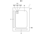
- FIG. 1 is a plan view showing a schematic configuration of a display device according to an embodiment of the present invention.
- 1 is a cross-sectional view showing a schematic configuration of a display area of a display panel provided in a display device of the present embodiment.
- FIG. 11 is a cross-sectional view showing a schematic configuration of a red light-emitting element as a comparative example.
- FIG. 4 is a diagram illustrating band levels of an electron transport layer, quantum dots included in a light-emitting layer, and a matrix included in a light-emitting layer, which are provided in the red light-emitting element shown in FIG. 3 as a comparative example.
- FIG. 1 is a cross-sectional view showing a schematic configuration of a red light emitting element provided in the display device of the present embodiment.
- 6 is a diagram illustrating the band levels of an electron transport layer, quantum dots included in a light-emitting layer, and a matrix included in a light-emitting layer, which are provided in the red light-emitting element illustrated in FIG. 5.
- FIG. 6 is a diagram for explaining a region formed between quantum dots when two adjacent quantum dots are arranged close to each other among the multiple quantum dots contained in the light-emitting layer of the red light-emitting element shown in FIG.
- 6 is a diagram for explaining a region formed between quantum dots when two adjacent quantum dots among the multiple quantum dots contained in the light-emitting layer provided in the red light-emitting element shown in FIG. 5 are arranged at a slight distance from each other.
- 6A to 6C are diagrams illustrating an example of a process for forming a light-emitting layer provided in the red light-emitting element illustrated in FIG. 5 .
- 10A to 10C are diagrams for explaining a process for forming the light-emitting layer shown in FIG. 9 .
- 7A to 7C are diagrams illustrating another example of the process for forming the light-emitting layer provided in the red light-emitting element illustrated in FIG. 5 .
- 12A to 12C are diagrams for explaining a process for forming the light-emitting layer shown in FIG. 11 .
- 6 is a diagram illustrating a variation in the upper valence band level of a plurality of quantum dots included in a light-emitting layer of the red light-emitting element shown in FIG. 5 due to variations in size and composition of the quantum dots.
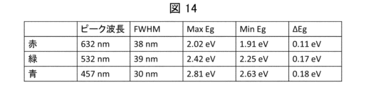
- 11 is a diagram showing the emission energy distribution due to variations in size and composition of quantum dots contained in the light-emitting layers of each color in red, green, and blue light-emitting elements provided in the display device of this embodiment.
- FIG. 1 is a plan view showing the schematic configuration of the display device 1 of this embodiment.
- the display device 1 includes a display panel 30, which includes a frame area NDA and a display area DA.
- the display area DA of the display panel 30 includes a plurality of pixels PIX, each of which includes a red subpixel RSUB, a green subpixel GSUB, and a blue subpixel BSUB.
- one pixel PIX is composed of a red subpixel RSUB, a green subpixel GSUB, and a blue subpixel BSUB, but this is not limiting.
- one pixel PIX may include subpixels of other colors in addition to the red subpixel RSUB, green subpixel GSUB, and blue subpixel BSUB.
- the scanning side driving circuit 31 and the data side driving circuit 32 are provided in the frame area NDA of the display panel 30 as an example, but this is not limited to this, and at least one of the scanning side driving circuit 31 and the data side driving circuit 32 may be external to the display panel 30.
- FIG. 2 is a cross-sectional view showing the schematic configuration of the display area DA of the display panel 30 provided in the display device 1 of this embodiment.
- a barrier layer 3 As shown in FIG. 2, in the display area DA of the display panel 30 provided in the display device 1, a barrier layer 3, a thin-film transistor layer 4 including a transistor TR, a red light-emitting element 5R, a green light-emitting element 5G, a blue light-emitting element 5B, a bank 23, a sealing layer 6, and a functional film 39 are provided on the substrate 12 in this order from the substrate 12 side.
- the red sub-pixel RSUB provided in the display area DA of the display panel 30 includes a red light-emitting element 5R
- the green sub-pixel GSUB provided in the display area DA of the display panel 30 includes a green light-emitting element 5G
- the blue sub-pixel BSUB provided in the display area DA of the display panel 30 includes a blue light-emitting element 5B.
- the substrate 12 may be, for example, a resin substrate made of a resin material such as polyimide, or a glass substrate.
- a resin substrate made of a resin material such as polyimide is used as the substrate 12 in order to make the display device 1 a flexible display device, a case where a resin substrate made of a resin material such as polyimide is used as the substrate 12 will be described as an example, but this is not limited to this. If the display device 1 is a non-flexible display device, a glass substrate can be used as the substrate 12.
- the barrier layer 3 is a layer that prevents foreign substances such as water and oxygen from penetrating the transistor TR, the red light-emitting element 5R, the green light-emitting element 5G, and the blue light-emitting element 5B, and can be composed of, for example, a silicon oxide film, a silicon nitride film, or a silicon oxynitride film, or a laminate film of these, formed by the CVD method.
- the transistor TR portion of the thin-film transistor layer 4 including the transistor TR includes the semiconductor film SEM and doped semiconductor films SEM' and SEM'', the inorganic insulating film 16, the gate electrode G, the inorganic insulating film 18, the inorganic insulating film 20, the source electrode S and the drain electrode D, and the planarization film 21, and the portion of the thin-film transistor layer 4 including the transistor TR other than the transistor TR portion includes the inorganic insulating film 16, the inorganic insulating film 18, the inorganic insulating film 20, and the planarization film 21.
- the semiconductor films SEM, SEM', and SEM'' may be made of, for example, low-temperature polysilicon (LTPS) or an oxide semiconductor (for example, an In-Ga-Zn-O-based semiconductor).
- LTPS low-temperature polysilicon
- oxide semiconductor for example, an In-Ga-Zn-O-based semiconductor.
- the gate electrode G and the source and drain electrodes S and D can be formed of a single layer or a multilayer film of a metal containing at least one of aluminum, tungsten, molybdenum, tantalum, chromium, titanium, and copper, for example.
- Inorganic insulating film 16, inorganic insulating film 18, and inorganic insulating film 20 can be composed of, for example, a silicon oxide film, a silicon nitride film, a silicon oxynitride film, or a laminate film of these films formed by the CVD method.
- the planarization film 21 can be made of a coatable organic material such as polyimide or acrylic, but it may also be made of an inorganic film.
- the red light-emitting element 5R included in the red subpixel RSUB includes an anode 22 above the planarization film 21, a functional layer 24R including a red light-emitting layer, and a cathode 25.
- the green light-emitting element 5G included in the green subpixel GSUB includes an anode 22 above the planarization film 21, a functional layer 24G including a green light-emitting layer, and a cathode 25.
- the blue light-emitting element 5B included in the blue subpixel BSUB includes an anode 22 above the planarization film 21, a functional layer 24B including a blue light-emitting layer, and a cathode 25.
- the insulating bank 23 covering the edge of the anode 22 can be formed by applying an organic material such as polyimide or acrylic and then patterning it by photolithography, but it may also be formed from an inorganic film.
- the red light emitting element 5R, the green light emitting element 5G, and the blue light emitting element 5B have a forward stack structure is described as an example, but this is not limited thereto, and the red light emitting element 5R, the green light emitting element 5G, and the blue light emitting element 5B may have an inverted stack structure.
- the red light emitting element 5R see FIG.
- the functional layer 24R including the red light emitting layer 24REM provided between the anode 22 and the cathode 25 can be formed, for example, by stacking a hole injection layer, a hole transport layer, a red light emitting layer, an electron transport layer, and an electron injection layer in this order from the anode 22 side.
- the functional layer 24R including the red light emitting layer 24REM one or more of the hole injection layer, hole transport layer, electron transport layer, and electron injection layer other than the red light emitting layer 24REM may be omitted as appropriate.
- the functional layer 24R including the red light-emitting layer 24REM is constructed by stacking a hole transport layer 24HT, a red light-emitting layer 24REM, and an electron transport layer 24ET in this order from the anode 22 side, but the present invention is not limited to this.
- the green light-emitting element 5G which has a forward stack structure, includes an anode 22 and a cathode 25 provided as an upper layer above the anode 22.
- the functional layer 24G including the green light-emitting layer provided between the anode 22 and the cathode 25 can be formed, for example, by stacking a hole injection layer, a hole transport layer, a green light-emitting layer, an electron transport layer, and an electron injection layer in this order from the anode 22 side.
- the functional layer 24G including the green light-emitting layer one or more layers of the hole injection layer, hole transport layer, electron transport layer, and electron injection layer other than the green light-emitting layer may be omitted as appropriate.
- the functional layer 24G including the green light-emitting layer is formed by stacking a hole transport layer, a green light-emitting layer, and an electron transport layer in this order from the anode 22 side, but this is not limited to this.
- the blue light-emitting element 5B which has a forward stack structure, includes an anode 22 and a cathode 25 provided as an upper layer above the anode 22.
- the functional layer 24B including the blue light-emitting layer provided between the anode 22 and the cathode 25 can be formed, for example, by stacking a hole injection layer, a hole transport layer, a blue light-emitting layer, an electron transport layer, and an electron injection layer in this order from the anode 22 side.
- the functional layer 24B including the blue light-emitting layer one or more layers of the hole injection layer, hole transport layer, electron transport layer, and electron injection layer other than the blue light-emitting layer may be omitted as appropriate.
- the functional layer 24B including the blue light-emitting layer is formed by stacking a hole transport layer, a blue light-emitting layer, and an electron transport layer in this order from the anode 22 side, but this is not limited to this.
- the red light-emitting element having an inverted stack structure includes a cathode and an anode provided as an upper layer above the cathode, and the functional layer including the red light-emitting layer 24REM provided between the cathode and the anode can be constructed, for example, by stacking an electron injection layer, an electron transport layer, a red light-emitting layer, a hole transport layer, and a hole injection layer in this order from the cathode side.
- the functional layers including the red light-emitting layer 24REM one or more of the electron injection layer, electron transport layer, hole transport layer, and hole injection layer other than the red light-emitting layer 24REM may be omitted as appropriate.
- a green light-emitting element having an inverted stack structure includes a cathode and an anode provided as an upper layer above the cathode, and a functional layer including a green light-emitting layer provided between the cathode and the anode can be constructed, for example, by stacking an electron injection layer, an electron transport layer, a green light-emitting layer, a hole transport layer, and a hole injection layer in this order from the cathode side.
- the functional layers including the green light-emitting layer one or more of the electron injection layer, electron transport layer, hole transport layer, and hole injection layer other than the green light-emitting layer may be omitted as appropriate.
- the blue light-emitting element having an inverted stack structure includes a cathode and an anode provided as an upper layer above the cathode, and the functional layer including the blue light-emitting layer provided between the cathode and the anode can be constructed, for example, by stacking an electron injection layer, an electron transport layer, a blue light-emitting layer, a hole transport layer, and a hole injection layer in this order from the cathode side.
- the functional layers including the blue light-emitting layer one or more of the electron injection layer, electron transport layer, hole transport layer, and hole injection layer other than the blue light-emitting layer may be omitted as appropriate.
- the material used for the hole injection layer is not particularly limited as long as it is a hole injection material that can stabilize the injection of holes into the light-emitting layer.
- a composite of poly(3,4-ethylenedioxythiophene) (PEDOT) and polystyrene sulfonic acid (PSS) (PEDOT:PSS) can be used.
- Materials used for the hole transport layer may include organic materials such as poly[(9,9-dioctylfluorenyl-2,7-diyl)-co-(4,4'-(N-(4-sec-butylphenyl))diphenylamine)] (TFB), N,N'-bis(4-butylphenyl)-N,N'-bis(phenyl)-benzidine (poly-TPD) or polyvinylcarbazole (PVK), or nanoparticles with hole transport properties such as NiO particles.
- organic materials such as poly[(9,9-dioctylfluorenyl-2,7-diyl)-co-(4,4'-(N-(4-sec-butylphenyl))diphenylamine)] (TFB), N,N'-bis(4-butylphenyl)-N,N'-bis(phenyl)-benzidine (poly-TPD) or polyviny
- the material used for the electron transport layer may be, for example, an organic material such as 2,2',2"-(1,3,5-benzintriyl)-tris(1-phenyl-1-H-benzimidazole) (TPBi), or nanoparticles with electron transport properties such as ZnO particles.
- organic material such as 2,2',2"-(1,3,5-benzintriyl)-tris(1-phenyl-1-H-benzimidazole) (TPBi), or nanoparticles with electron transport properties such as ZnO particles.
- the material used for the electron injection layer is not particularly limited as long as it is an electron injection material that can stabilize the injection of electrons into the light-emitting layer.
- alkali metals or alkaline earth metals such as aluminum, strontium, calcium, lithium, cesium, magnesium oxide, aluminum oxide, strontium oxide, lithium oxide, lithium fluoride, magnesium fluoride, strontium fluoride, calcium fluoride, barium fluoride, cesium fluoride, polymethyl methacrylate polystyrene sodium sulfonate, oxides of alkali metals or alkaline earth metals, fluorides of alkali metals or alkaline earth metals, organic complexes of alkali metals, etc. can be used.
- the functional layer 24R including the red light-emitting layer 24REM, the functional layer 24G including the green light-emitting layer, and the functional layer 24B including the blue light-emitting layer each have a hole transport layer formed in the same process using the same material, and an electron transport layer formed in the same process using the same material, but this is not limited to this example.
- the hole injection layers included in the functional layers 24R, 24G, and 24B may be formed in the same process using the same material, or may be formed from different materials, and the hole injection layers included in two of the functional layers 24R, 24G, and 24B may be formed in the same process using the same material, and only the hole injection layer included in the remaining functional layer may be formed in a different process using a different material.
- each hole transport layer included in each functional layer 24R, 24G, 24B may be formed from a different material, and the hole transport layers included in two of the functional layers 24R, 24G, 24B may be formed from the same material in the same process, and only the hole transport layer included in the remaining functional layer may be formed from a different material in a different process.
- each electron transport layer included in each functional layer 24R, 24G, 24B may be formed from a different material, and the electron transport layers included in two of the functional layers 24R, 24G, 24B may be formed from the same material in the same process, and only the electron transport layer included in the remaining functional layer may be formed from a different material in a different process.
- the electron injection layers included in each of the functional layers 24R, 24G, and 24B may be formed in the same process using the same material, or may be formed in different materials.
- the electron injection layers included in two of the functional layers 24R, 24G, and 24B may be formed in the same process using the same material, and only the electron injection layer included in the remaining functional layer may be formed in a separate process using a different material.
- the red light-emitting element 5R, the green light-emitting element 5G, and the blue light-emitting element 5B are all QLEDs (quantum dot light-emitting diodes) will be described as an example, but this is not limited thereto, and it is sufficient that one or more of the red light-emitting element 5R, the green light-emitting element 5G, and the blue light-emitting element 5B are QLEDs.
- the remaining two may be OLEDs (organic light-emitting diodes), and for example, if two of the red light-emitting element 5R, the green light-emitting element 5G, and the blue light-emitting element 5B are QLEDs, the remaining one may be an OLED.
- OLEDs organic light-emitting diodes
- the light emitting layer of each light emitting element includes quantum dots.
- the quantum dots may have, for example, a core structure, a core/shell structure, a core/shell/shell structure, or a shell structure in which the core/ratio is continuously changed.
- the shell may completely cover the core, or may cover only a part of the core.
- the core part may be composed of, for example, Si, C, etc.; in the case of a binary element, the core part may be composed of, for example, CdSe, CdS, CdTe, InP, GaP, InN, ZnSe, ZnS, ZnTe, etc.; in the case of a ternary element, the core part may be composed of, for example, CdSeTe, GaInP, ZnSeTe, etc.; and in the case of a quaternary element, the core part may be composed of, for example, AIGS, etc.
- the shell portion can be composed of, for example, CdS, CdTe, CdSe, ZnS, ZnSe, ZnTe, etc.
- the shell portion can be composed of, for example, CdSSe, CdTeSe, CdSTe, ZnSSe, ZnSTe, ZnTeSe, AIP, etc.
- the quantum dots described above include organic or inorganic ligands (e.g., halogen ligands) disposed on or near the surface of the quantum dots
- the quantum dots refer to those that include organic or inorganic ligands (e.g., halogen ligands).
- the maximum width of the quantum dot excluding the ligand portion is 100 nm or less.
- the shape of the quantum dot excluding the ligand portion may be within the range that satisfies the above maximum width, and is not particularly restricted, and is not limited to a spherical three-dimensional shape (circular cross-sectional shape). For example, it may be a polygonal cross-sectional shape, a rod-shaped three-dimensional shape, a branch-shaped three-dimensional shape, a three-dimensional shape with unevenness on the surface, or a combination of these.
- the red light emitting element 5R, green light emitting element 5G, and blue light emitting element 5B have a forward stack structure in which the cathode 25 is disposed above the anode 22.
- the anode 22 may be formed from an electrode material that reflects visible light
- the cathode 25 may be formed from an electrode material that transmits visible light.
- the anode 22 may be formed from an electrode material that transmits visible light
- the cathode 25 may be formed from an electrode material that reflects visible light.
- the cathode 25 should be formed from an electrode material that reflects visible light, and the anode 22 should be formed from an electrode material that transmits visible light; in order to achieve a bottom emission type, the cathode 25 should be formed from an electrode material that transmits visible light, and the anode 22 should be formed from an electrode material that reflects visible light.
- the electrode material that reflects visible light is not particularly limited as long as it can reflect visible light and has electrical conductivity, but examples include metal materials such as Al, Mg, Li, and Ag, alloys of the above metal materials, laminates of the above metal materials and transparent metal oxides (e.g., indium tin oxide, indium zinc oxide, indium gallium zinc oxide, etc.), and laminates of the above alloys and the above transparent metal oxides.
- metal materials such as Al, Mg, Li, and Ag
- alloys of the above metal materials such as Al, Mg, Li, and Ag
- alloys of the above metal materials such as Al, Mg, Li, and Ag
- laminates of the above metal materials and transparent metal oxides e.g., indium tin oxide, indium zinc oxide, indium gallium zinc oxide, etc.
- laminates of the above alloys and the above transparent metal oxides e.g., indium tin oxide, indium zinc oxide, indium gallium zinc oxide, etc.
- electrode materials that transmit visible light are not particularly limited as long as they are capable of transmitting visible light and have electrical conductivity, but examples include transparent metal oxides (e.g., indium tin oxide, indium zinc oxide, indium gallium zinc oxide, etc.), thin films made of metal materials such as Al and Ag, and nanowires made of metal materials such as Al and Ag.
- transparent metal oxides e.g., indium tin oxide, indium zinc oxide, indium gallium zinc oxide, etc.
- thin films made of metal materials such as Al and Ag
- nanowires made of metal materials such as Al and Ag.
- the anode 22 and the cathode 25 can be formed by a method that is generally used for forming electrodes, such as physical vapor deposition (PVD) methods such as vacuum deposition, sputtering, EB deposition, and ion plating, or chemical vapor deposition (CVD).
- PVD physical vapor deposition
- CVD chemical vapor deposition
- the method for patterning the anode 22 and the cathode 25 is not particularly limited as long as it can be formed into the desired pattern with high precision, but specific examples include photolithography and inkjet methods.
- the sealing layer 6 is a light-transmitting film, and can be composed of, for example, an inorganic sealing film 26 that covers the cathode 25, an organic film 27 that is above the inorganic sealing film 26, and an inorganic sealing film 28 that is above the organic film 27.
- the sealing layer 6 prevents foreign matter such as water and oxygen from penetrating into the red light-emitting element 5R, the green light-emitting element 5G, and the blue light-emitting element 5B.
- the inorganic sealing film 26 and the inorganic sealing film 28 are inorganic films, and may be formed, for example, by a CVD method, such as a silicon oxide film, a silicon nitride film, or a silicon oxynitride film, or a laminated film of these.
- the organic film 27 is a light-transmitting organic film with a planarizing effect, and may be formed, for example, by a coatable organic material such as acrylic.
- the organic film 27 may be formed, for example, by an inkjet method.
- the sealing layer 6 is formed of two inorganic films and one organic film provided between the two inorganic films, but the order of lamination of the two inorganic films and one organic film is not limited to this. Furthermore, the sealing layer 6 may be formed only of an inorganic film, may be formed only of an organic film, may be formed of one inorganic film and two organic films, or may be formed of two or more inorganic films and two or more organic films.
- the functional film 39 is, for example, a film having at least one of an optical compensation function, a touch sensor function, and a protective function.
- the inventors of the present disclosure came up with the idea of suppressing the deterioration of the characteristics of the light-emitting layer by using a matrix that fills at least a portion of the space between each of the multiple quantum dots (QDs) in the light-emitting layer.
- QDs quantum dots
- the matrix filling at least a part of the space between the quantum dots QDs in the light-emitting layer is a single matrix made of ZnS, a metal sulfide
- the single matrix is formed in a relatively low temperature process (e.g., 25°C or higher and 100°C or lower) in order to maintain good luminous efficiency of the quantum dots contained in the light-emitting layer, the single matrix will contain defects that can become paths for non-luminescent recombination, resulting in non-luminescent leakage in the light-emitting layer.
- a single matrix made of ZnS, a metal sulfide is formed in a relatively high temperature process of about several hundred degrees in order to reduce the above-mentioned defects, it may affect the quantum dots contained in the light-emitting layer, decreasing the luminous efficiency of the quantum dots. Therefore, even if good luminous characteristics are obtained in the case of a light-emitting layer containing a single matrix made of ZnS, a metal sulfide, there is room for improvement in the light-emitting layer as a whole.
- the inventors of the present disclosure have discovered that by forming the single matrix MRr from a metal halide MHa such as copper iodide (CuI) or silver iodide (AgI), as in the case of the red light-emitting element 5Rr, which is a comparative example described below, it is possible to realize a light-emitting element having a light-emitting layer that has good luminous efficiency and good suppression of non-luminous leakage, compared to a case in which the single matrix MRr is formed from the metal sulfide ZnS.
- a metal halide MHa such as copper iodide (CuI) or silver iodide (AgI)
- the single matrix MRr is made of a metal halide MHa such as copper iodide (CuI) or silver iodide (AgI) as in the comparative example red light emitting element 5Rr described later, a highly crystalline single matrix MRr can be produced even at relatively low temperatures (e.g., 25°C or higher and 100°C or lower), for example, at room temperature, and a light emitting layer with good luminous efficiency and good suppression of non-luminous leakage can be realized.
- the single matrix means a matrix made of one type of compound.
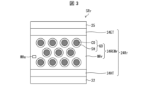
- Figure 3 is a cross-sectional view showing the schematic configuration of a red light-emitting element 5Rr, which is a comparative example.
- the configurations with a lowercase “r" at the end of the reference numerals in FIG. 3 indicate comparative example configurations that differ from the configuration of this embodiment described below.
- the comparative red light-emitting element 5Rr has a configuration that includes a functional layer 24Rr that includes a red light-emitting layer 24REMr that has a single matrix MRr composed of metal halide MHa, and differs from the configuration of the red light-emitting element 5R of this embodiment shown in FIG. 5 described below.
- the red light-emitting element 5Rr includes an anode 22, a cathode 25, and a functional layer 24Rr including a red light-emitting layer 24REMr disposed between the anode 22 and the cathode 25.
- the functional layer 24Rr including the red light-emitting layer 24REMr is configured by stacking, in order from the anode 22 side, a hole transport layer 24HT, a red light-emitting layer 24REMr, and an electron transport layer 24ET.
- the red light-emitting layer 24REMRr includes a plurality of quantum dots QDs including a core CO and a shell SH, and a single matrix MRr composed of metal halide MHa composed of a metal element and a halogen element arranged to fill the space between each of the plurality of quantum dots QDs.
- the metal halide MHa constituting the single matrix MRr provided in the red light-emitting element 5Rr which is a comparative example, is described as being, for example, copper iodide (CuI) composed of the metal element copper (Cu) and the halogen element iodine (I), but is not limited to this, and the metal halide MHa constituting the single matrix MRr may be silver iodide (AgI) composed of the metal element silver (Ag) and the halogen element iodine (I).
- the metal halide MHa constituting the single matrix MRr is a material with a narrower band gap than ZnS, which is a metal sulfide.
- FIG. 4 is a diagram showing the band levels of the electron transport layer 24ET, the quantum dots QD contained in the red light-emitting layer 24REMR, and the single matrix MRr contained in the red light-emitting layer 24REMR, which are provided in the red light-emitting element 5Rr shown in FIG. 3, which is a comparative example.
- the inventors of the present disclosure have found that when the single matrix MRr is made of a metal halide MHa such as copper iodide (CuI) or silver iodide (AgI) as in the comparative example red light emitting element 5Rr described above, the upper valence band level QD(VBM) of the quantum dot QD and the upper valence band level MRr(VBM) of the single matrix MRr become closer, as shown in FIG. 4, and the band gap of the quantum dot QD and the band gap of the single matrix MRr also become closer.
- a metal halide MHa such as copper iodide (CuI) or silver iodide (AgI)
- CuI copper iodide
- AgI silver iodide
- the band gap of a quantum dot QD that emits red light is 2.0 eV
- the band gap of a quantum dot QD that emits green light is 2.3 eV
- the band gap of a quantum dot QD that emits blue light is 2.8 eV.
- the single matrix MRr is constructed using copper iodide (CuI), which has a band gap of 3.1 eV, instead of ZnS, a metal sulfide with a band gap of 3.8 eV, as described above, the upper valence band level QD(VBM) of the quantum dot QD and the upper valence band level MRr(VBM) of the single matrix MRr become closer, and the band gap of the quantum dot QD and the band gap of the single matrix MRr also become closer.
- CuI copper iodide
- the holes H which are carriers injected into the red light-emitting layer 24REMR, are conducted through the single matrix MRr without passing through the quantum dots QD and reach the interface between the red light-emitting layer 24REMR and the electron transport layer 24ET.
- the inventors of the present disclosure therefore propose a light-emitting element having a light-emitting layer with even better light-emitting efficiency and even better suppression of non-luminous leakage, and a display device including the light-emitting element.
- FIG. 5 is a cross-sectional view showing the schematic configuration of a red light-emitting element 5R provided in the display device 1 of this embodiment.
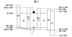
- FIG. 6 is a diagram showing the band levels of the electron transport layer 24ET, the quantum dots QD contained in the red light-emitting layer 24REM, and the matrix MR contained in the red light-emitting layer 24REM, which are provided in the red light-emitting element 5R shown in FIG. 5.
- the red light-emitting element 5R provided in the display device 1 includes an anode 22, a cathode 25, and a red light-emitting layer 24REM provided between the anode 22 and the cathode 25.
- the functional layer 24R which includes the red light-emitting layer 24REM, is constructed by stacking, in this order from the anode 22 side, a hole transport layer 24HT, a red light-emitting layer 24REM, and an electron transport layer 24ET.
- the red light-emitting layer 24REM includes a plurality of quantum dots QDs each including a core CO and a shell SH, and a matrix MR including a plurality of metal halides MHa1, MHa2, and MHa3 each consisting of a metal element and a halogen element, which are provided at least partially between each of the quantum dots QDs.
- a matrix MR including a plurality of metal halides MHa1, MHa2, and MHa3 each consisting of a metal element and a halogen element, which are provided at least partially between each of the quantum dots QDs.
- the matrix MR is provided so as to fill the space between each of the quantum dots QDs, but this is not limited to this, and even if the matrix MR is provided in a portion of the space between each of the quantum dots QDs, the effect of increasing the luminous efficiency and the suppression of non-luminous leakage can be obtained.
- the matrix MR includes a first portion including a first metal halide and a second portion including a second metal halide different from the first metal halide, and the first portion is disposed closer to the cathode 25 than the second portion.
- the first part containing a first metal halide is located closer to the cathode 25 than the second part containing a second metal halide different from the first metal halide.
- the matrix MR1 containing the metal halide MHa1 is the first part
- at least one of the matrix MR2 containing the metal halide MHa2 and the matrix MR3 containing the metal halide MHa3 is the second part
- the matrix MR2 containing the metal halide MHa2 is the first part
- the matrix MR3 containing the metal halide MHa3 is the second part.
- different compounds include not only compounds composed of different elements, but also compounds composed of the same elements but with different composition ratios.
- the single matrix MRr is composed of one type of metal halide MHa, which is one type of compound such as copper iodide (CuI) or silver iodide (AgI). Therefore, the upper level MRr(VBM) of the valence band of the single matrix MRr and the lower level MRr(CBM) of the conduction band of the single matrix MRr each become one quantum level. Therefore, the positive hole H, which is a carrier injected into the red light-emitting layer 24REMr, becomes the valence band of the single matrix MRr.
- CuI copper iodide
- AgI silver iodide
- the electrons E which are carriers injected into the red light-emitting layer 24REMr, pass through the level MRr (VBM) at the top of the electron band and reach the interface between the red light-emitting layer 24REMR and the electron transport layer 24ET, and pass through the level MRr (CBM) at the bottom of the conduction band of the single matrix MRr and reach the interface between the red light-emitting layer 24REMR and the hole transport layer 24HT. Since non-radiative recombination is likely to occur, non-radiative leakage may occur in the red light-emitting layer 24REMR, and there is room for improvement in the red light-emitting layer 24REMR as a whole.
- VBM level MRr
- CBM level MRr
- the matrix MR includes a first portion including a first metal halide and a second portion including a second metal halide different from the first metal halide. Therefore, as shown in FIG. 6, the level of the upper end of the valence band of the matrix MR and the level of the lower end of the conduction band of the matrix MR each have a plurality of different quantum levels.
- the holes H which are carriers injected into the red light emitting layer 24REM, cannot pass through the level of the upper end of the valence band of the matrix MR and are suppressed from reaching the interface between the red light emitting layer 24REM and the electron transport layer 24ET, and the electrons E, which are carriers injected into the red light emitting layer 24REM, cannot pass through the level of the lower end of the conduction band of the matrix MR and are suppressed from reaching the interface between the red light emitting layer 24REM and the hole transport layer 24HT.
- the level of the upper end of the valence band of the first portion which is located closer to the cathode 25 than the second portion, is deeper than the level of the upper end of the valence band of the second portion. Therefore, as shown in FIG.
- the level MR2&3 (VBM) of the upper end of the valence band of the portion where the matrix MR2 containing the metal halide MHa2 and the matrix MR3 containing the metal halide MHa3 are stacked is deeper than the level MR3 (VBM) of the upper end of the valence band of the matrix MR3 containing the metal halide MHa3, and the level MR3 (VBM) of the upper end of the valence band of the portion where the matrix MR1 containing the metal halide MHa1 and the matrix MR2 containing the metal halide MHa2 are stacked is deeper than the level MR3 (VBM) of the upper end of the valence band of the matrix MR3 containing the metal halide MHa1.
- MR1&2 (VBM) is deeper than the level MR2&3 (VBM) at the top of the valence band of the portion where the matrix MR2 containing the metal halide MHa2 and the matrix MR3 containing the metal halide MHa3 are stacked, and the level MR1 (VBM) at the top of the valence band of the matrix MR1 containing the metal halide MHa1 is deeper than the level MR1&2 (VBM) at the top of the valence band of the portion where the matrix MR1 containing the metal halide MHa1 and the matrix MR2 containing the metal halide MHa2 are stacked.
- the injected carriers, the holes H pass through a stepped potential, and it becomes more difficult for the holes H to pass as they move through the red light-emitting layer 24REM.
- the level of the conduction band minimum of the first portion which is provided closer to the cathode 25 than the second portion, is deeper than the level of the conduction band minimum of the second portion. Therefore, as shown in FIG. 6, in the red light emitting element 5R of this embodiment, the level MR2&3(CBM) of the conduction band minimum of the portion where the matrix MR2 containing the metal halide MHa2 and the matrix MR3 containing the metal halide MHa3 are stacked is deeper than the level MR3(CBM) of the conduction band minimum of the matrix MR3 containing the metal halide MHa3, and the level MR3(CBM) of the conduction band minimum of the portion where the matrix MR1 containing the metal halide MHa1 and the matrix MR2 containing the metal halide MHa2 are stacked is deeper than the level MR3(CBM) of the conduction band minimum of the portion where the matrix MR1 containing the metal halide MHa1 and the matrix
- MR1&2 is deeper than the conduction band lower edge level MR2&3 (CBM) of the portion where the matrix MR2 containing the metal halide MHa2 and the matrix MR3 containing the metal halide MHa3 are stacked, and the conduction band lower edge level MR1 (CBM) of the matrix MR1 containing the metal halide MHa1 is deeper than the conduction band lower edge level MR1&2 (CBM) of the portion where the matrix MR1 containing the metal halide MHa1 and the matrix MR2 containing the metal halide MHa2 are stacked.
- the injected carrier electrons E pass through a stepped potential, and as the electrons E move through the red light-emitting layer 24REM, it becomes more difficult for them to pass.
- the metal halide MHa1 contained in the matrix MR1, the metal halide MHa2 contained in the matrix MR2, and the metal halide MHa3 contained in the matrix MR3 are copper iodides with different composition ratios, but this is not limited thereto, and may be, for example, silver iodides with different composition ratios.
- the metal halide MHa1, the metal halide MHa2, and the metal halide MHa3 are compounds composed of the same element and have different composition ratios, but this is not limited thereto, and may be compounds composed of different elements.
- the composition ratio of the compound composed of the same element is different in each matrix unit contained in the matrix MR, but this is not limited thereto, and a certain matrix contained in the matrix MR may be composed of two or more different compounds, and a certain matrix contained in the matrix MR may be composed of a compound whose composition ratio changes continuously in the thickness direction.
- the matrix MR is composed of the matrix MR1, the matrix MR2, and the matrix MR3 is described as an example, but the present invention is not limited to this.
- the matrix MR may be composed of, for example, the matrix MR1 and the matrix MR2, or may be composed of four or more different matrices.
- the (metal element/halogen element) ratio of the metal halide MHa1 contained in the matrix MR1 is smaller than the (metal element/halogen element) ratio of the metal halide MHa2 contained in the matrix MR2 and the (metal element/halogen element) ratio of the metal halide MHa3 contained in the matrix MR3, and the (copper element/iodine element) ratio of the copper iodide contained in the matrix MR1 is smaller than the (copper element/iodine element) ratio of the copper iodide contained in the matrix MR2 and the (copper element/iodine element) ratio of the copper iodide contained in the matrix MR3.
- the copper iodide contained in the matrices MR2 and MR3 is P-type copper iodide
- the copper iodide contained in the matrix MR1 is close to intrinsic copper iodide.
- the (metal element/halogen element) ratio value is the ratio value of the metal element to the halogen element in the compounds contained in the corresponding matrices, for example, matrix MR1, matrix MR2, and matrix MR3.
- P-type copper iodide which has a high mobility of holes H
- matrices MR2 and MR3 which are provided closer to the anode 22 than matrix MR1. Therefore, even if, for example, ZnO particles, which have a high mobility of electrons, are used as the electron transport layer 24ET, the carrier balance between holes H and electrons E can be improved.
- the carrier density (carrier density of holes H) of the copper iodide contained in the above-mentioned matrices MR2 and MR3 is preferably 1 ⁇ 10 cm ⁇ 3 or more and 1 ⁇ 10 cm ⁇ 3 or less, and the value of the (copper element/iodine element) ratio of the copper iodide contained in the above-mentioned matrices MR2 and MR3 is preferably appropriately determined to be, for example, 0.5 or more and 0.99 or less.
- the copper iodide contained in the above-mentioned matrix MR1 has a (copper element/iodine element) ratio of 0.95
- the copper iodide contained in the above-mentioned matrix MR2 has a (copper element/iodine element) ratio of 0.97
- the copper iodide contained in the above-mentioned matrix MR3 has a (copper element/iodine element) ratio of 0.99.
- the red light emitting element 5R of this embodiment in order to prevent the holes H, which are carriers injected into the red light emitting layer 24REM, from being conducted through the matrix MR without passing through the quantum dots QD and reaching the interface between the red light emitting layer 24REM and the electron transport layer 24ET, at least the level MR1(VBM) at the upper end of the valence band of the matrix MR1 is made deeper than the level QD(VBM) at the upper end of the valence band of the quantum dots QD, as shown in FIG. 6, but is not limited to this.
- the level MR1(VBM) of the upper end of the valence band of the matrix MR1 deeper by 0.3 eV or more than the level QD(VBM) of the upper end of the valence band of the quantum dot QD, it is possible to further prevent the holes H, which are carriers injected into the red light-emitting layer 24REM, from being conducted through the matrix MR without passing through the quantum dot QD and reaching the interface between the red light-emitting layer 24REM and the electron transport layer 24ET.
- the metal halide MHa1 contained in matrix MR1, the metal halide MHa2 contained in matrix MR2, and the metal halide MHa3 contained in matrix MR3 each contain one type of metal element (copper element or silver element), but this is not limited to this, and at least one of the metal halide MHa1 contained in matrix MR1, the metal halide MHa2 contained in matrix MR2, and the metal halide MHa3 contained in matrix MR3 may contain two or more types of metal elements.
- Each of the metal halide MHa1 contained in the matrix MR1, the metal halide MHa2 contained in the matrix MR2, and the metal halide MHa3 contained in the matrix MR3 may contain at least a first metal element and a second metal element as metal elements.
- the first metal element may be Cu or Ag
- the second metal element may be one metal element selected from the N-type dopant metal elements Zn, Cd, Sn, Ti, Zr, Ta, and W.
- the band and Fermi level of the matrix can be controlled more widely.
- the ratio value of (the second metal element/the first metal element) of the metal halide MHa1 contained in the matrix MR1 is preferably greater than the ratio values of (the second metal element/the first metal element) of the metal halide MHa2 contained in the matrix MR2 and the metal halide MHa3 contained in the matrix MR3.
- the metal halide MHa1 contained in the matrix MR1 may be composed of copper (Cu), zinc (Zn), and iodine (I) in a first composition ratio
- the metal halide MHa2 contained in the matrix MR2 may be composed of copper (Cu), zinc (Zn), and iodine (I) in a second composition ratio different from the first composition ratio
- the metal halide MHa3 contained in the matrix MR3 may be composed of copper (Cu), zinc (Zn), and iodine (I) in a third composition ratio different from the first composition ratio and the second composition ratio.
- the carrier density of the metal halide MHa1 contained in the matrix MR1 is 1 ⁇ 10 15 cm -3 or more and 1 ⁇ 10 19 cm -3 or less
- the ratio of (copper element/iodine element) of the metal halide MHa1 contained in the matrix MR1 is 0.95 or more and 1.0 or less
- the ratio of (zinc element/copper element) of the metal halide MHa1 contained in the matrix MR1 is 0.01 or more and 0.5 or less, as appropriate.
- the carrier density of the metal halide MHa2 contained in the matrix MR2 and the metal halide MHa3 contained in the matrix MR3 is preferably 1 ⁇ 10 18 cm -3 or more and 1 ⁇ 10 20 cm -3 or less
- the ratio of (copper element/iodine element) of the metal halide MHa2 and the metal halide MHa3 is preferably 0.5 or more and 0.99 or less
- the ratio of (zinc element/copper element) of the metal halide MHa2 and the metal halide MHa3 is preferably 1 ⁇ 10 -11 or more and 0.01 or less, as appropriate.
- each of the multiple quantum dots QDs is embedded in a matrix MR, i.e., the matrix MR surrounds each of the multiple quantum dots QDs, but this is not limited to this, and it is sufficient that the matrix MR is provided at least partially between each of the multiple quantum dots QDs.
- FIG. 7 is a diagram for explaining the region R formed between the quantum dots QD1 and QD2 when two adjacent quantum dots QD1 and QD2 are arranged close to each other among the multiple quantum dots QD contained in the red light-emitting layer 24REM provided in the red light-emitting element 5R shown in FIG. 5.
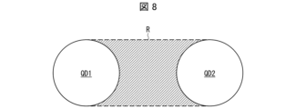
- FIG. 8 is a diagram for explaining the region R formed between the quantum dots QD1 and QD2 when two adjacent quantum dots QD1 and QD2 are arranged a short distance apart from each other among the multiple quantum dots QD contained in the red light-emitting layer 24REM provided in the red light-emitting element 5R shown in FIG. 5.
- the region R shown in Figs. 7 and 8 is a region surrounded by two straight lines (common circumscribing lines) tangent to the peripheries of two adjacent quantum dots QD1 and QD2 and the opposing peripheries of two adjacent quantum dots QD1 and QD2. Even when the two adjacent quantum dots QD1 and QD2 are arranged close to each other as shown in Fig. 7, or when the two adjacent quantum dots QD1 and QD2 are arranged slightly apart as shown in Fig. 8, the region R exists and is filled with the matrix MR. "The matrix MR is filled between the two adjacent quantum dots QD1 and QD2" means that the region R shown in Figs. 7 and 8 is filled or filled with the matrix MR. In the present disclosure, the two adjacent quantum dots QD1 and QD2 may be held by the presence of the matrix MR in the region R, and for example, at least a part of the region R may be filled with the matrix MR.
- the region R formed between two adjacent quantum dots QD1 and QD2 shown in Figures 7 and 8, i.e., the space between multiple quantum dots QD, is filled with a matrix MR as an example, but is not limited to this.
- the quantum dots QD1 and QD2 are held by the matrix MR present in the region R formed between two adjacent quantum dots QD1 and QD2, this means that at least a part of the region R is filled with the matrix MR, and includes not only the case where the matrix MR fills the entire region R, but also the case where the matrix MR fills only a part of the region R.
- the matrix MR may be formed so as to fill the regions (spaces) of the light-emitting layer other than the quantum dots QD.
- the matrix MR may be configured to form the outer edge of the light-emitting layer (e.g., the red light-emitting layer 24REM), and the quantum dots QD may be configured to be located away from the outer edge. That is, the matrix MR may contain the quantum dots QD.
- the matrix MR may contain the quantum dots QD.
- at least a part of the outer edge of the light-emitting layer may be composed of the matrix MR and the quantum dots QD.
- each of the quantum dots QD may be embedded in the matrix MR at intervals.
- the outer edge means the first surface of the light-emitting layer (e.g., the surface of the red light-emitting layer 24REM in contact with the electron transport layer 24ET shown in FIG. 5) and the second surface of the light-emitting layer (e.g., the surface of the red light-emitting layer 24REM in contact with the hole transport layer 24HT shown in FIG. 5).
- the matrix MR may include a continuous film.
- a continuous film means a film that is not divided by materials other than the material that constitutes the continuous film.
- the continuous film may be an integrated film that is connected without interruption by chemical bonds of the metal halides MHa1, MHa2, and MHa3 contained in the matrix MR.
- a matrix MR is provided at least partially between each of the multiple quantum dots QD" means that the matrix MR is filled between at least two quantum dots QD.
- the matrix MR is filled between multiple quantum dots QD
- the matrix MR is present in the greatest amount between the quantum dots QD, and therefore the effect of the matrix MR between the quantum dots QD is the strongest, which is desirable as it provides a very high effect.
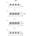
- FIG. 9 shows an example of a process for forming the red light-emitting layer 24REM provided in the red light-emitting element 5R shown in FIG. 5.
- FIG. 10 is a diagram illustrating the process of forming the red light-emitting layer 24REM shown in FIG. 9.
- the red light-emitting layer 24REM which includes a plurality of quantum dots QD, a matrix MR1 including a metal halide MHa1, a matrix MR2 including a metal halide MHa2, and a matrix MR3 including a metal halide MHa3, can be formed by a solution method such as the SILAR method (Successive Ionic Layer Adsorption and Reaction) at a temperature of, for example, 25°C or higher and 100°C or lower.
- SILAR method Successessive Ionic Layer Adsorption and Reaction
- the process of forming the red light-emitting layer 24REM provided in the red light-emitting element 5R includes a process (S1 process in FIG. 9 and FIG. 10) of forming a quantum dot layer of a predetermined thickness containing a plurality of quantum dots QD on a substrate (e.g., on a hole transport layer 24HT provided on a substrate), a first solution treatment process of treating the quantum dot layer with a first solution containing one of the ions of the metal element (e.g., Cu) and the ions of the halogen element (e.g., I), and a second solution treatment process of treating the quantum dot layer with a second solution containing the other of the ions of the metal element (e.g., Cu) and the ions of the halogen element (e.g., I) after the first solution treatment process.
- a process S1 process in FIG. 9 and FIG. 10
- a solution that serves as an ion source of the metal element e.g., Cu
- a solution that serves as an ion source of the metal element e.g., Cu
- the quantum dot layer may be immersed in a solution that serves as an ion source of the metal element (e.g., Cu) to adsorb Cu ions onto the quantum dot QD surface.
- a rinsing process (step S3 in Figures 9 and 10) may be performed as necessary to remove excess Cu ions.
- a solution e.g., a 0.025 mol/l KI solution
- a solution that serves as an ion source for the halogen element (e.g., I) may be applied to the quantum dot layer to adsorb I ions onto the quantum dot QD surface and react with Cu ions
- the quantum dot layer may be immersed in a solution that serves as an ion source for the halogen element (e.g., I) to adsorb I ions onto the quantum dot QD surface and react with Cu ions.
- the amount of solution used as the I ion source is adjusted so that the copper iodide (copper element/iodine element) ratio in the matrix MR3 is 0.99.
- a rinsing step (step S5 in Figures 9 and 10) may be performed as necessary to remove excess I ions.
- a light-emitting layer containing quantum dots QD embedded in a matrix MR3 containing copper iodide, which is a metal halide MHa3, can be formed (step S6 in Figures 9 and 10).
- step S4 in FIG. 9 the amount of the solution serving as the I ion source is adjusted so that the copper iodide contained in the matrix MR2 has a (copper element/iodine element) ratio of 0.97. This allows the formation of a light-emitting layer containing quantum dots QD embedded in the matrix MR2 containing copper iodide, which is the metal halide MHa2.
- the organic ligands attached to the quantum dots QDs are removed before the first solution treatment step (step S2 in FIG. 9) by, for example, washing the surface of the quantum dots QDs with ethanol or the like.
- the solvent used in the first solution treatment step is a solvent that dissolves the organic ligands
- the organic ligands can be removed in the first solution treatment step (step S2 in FIG. 9), and therefore the prior organic ligand removal step can be omitted.
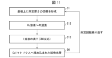
- FIG. 11 shows another example of a process for forming the red light-emitting layer 24REM provided in the red light-emitting element 5R shown in FIG. 5.
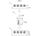
- FIG. 12 is a diagram illustrating the process of forming the red light-emitting layer 24REM shown in FIG. 11.
- the red light-emitting layer 24REM which includes a plurality of quantum dots QD, a matrix MR1 including a metal halide MHa1, a matrix MR2 including a metal halide MHa2, and a matrix MR3 including a metal halide MHa3, can be formed by a solution method such as the CBD method (Chemical Bath Deposition) at a temperature of, for example, 25°C or higher and 100°C or lower.
- CBD method Cert Control Bath Deposition
- the process of forming the red light-emitting layer 24REM provided in the red light-emitting element 5R includes a process of forming a quantum dot layer of a predetermined thickness containing a plurality of quantum dots QD on a substrate (e.g., on a hole transport layer 24HT provided on a substrate) (step S1 in Figs. 11 and 12), an immersion process of immersing the substrate on which the quantum dot layer has been formed in a first solution containing one of the ions of the metal element (e.g., Cu) and the ions of the halogen element (e.g., I) (step S12 in Fig.
- the substrate on which the quantum dot layer is formed is immersed in a solution (e.g., a 0.1 mol/l [Cu(S 2 O 3 )] complex solution) that serves as an ion source of the metal element (e.g., Cu).
- a solution e.g., a 0.1 mol/l [Cu(S 2 O 3 )] complex solution
- the metal element e.g., Cu
- step S13 in Figs. 11 and 12 while the substrate is immersed in the solution that serves as the ion source of the metal element (e.g., Cu), a solution that serves as the ion source of the halogen element (e.g., I) (e.g., 0.025 mol/l KI solution) is dropped to cause a CBD reaction.
- the ion source of the metal element e.g., Cu
- a solution that serves as the ion source of the halogen element e.g., I
- the amount of the solution that serves as the I ion source dropped is adjusted so that the ratio of (copper element/iodine element) of the copper iodide contained in the matrix MR3 becomes 0.99.
- a light-emitting layer containing quantum dots QD embedded in a matrix MR3 containing copper iodide, which is a metal halide MHa3, can be formed (step S6 in Figures 11 and 12).
- step S13 in FIG. 11 and FIG. 12 the amount of the solution that serves as the I ion source dropped is adjusted so that the copper iodide contained in the matrix MR2 has a ratio of (copper element/iodine element) of 0.97, thereby forming a light-emitting layer that includes quantum dots QD embedded in the matrix MR2 that contains copper iodide, which is the metal halide MHa2.
- the organic ligands attached to the quantum dots QDs are removed before the immersion step (step S12 in FIG. 11), for example by cleaning the surface of the quantum dots QDs with ethanol or the like.
- the solvent used in the immersion step is a solvent that dissolves the organic ligands
- the organic ligands can be removed in the immersion step (step S12 in FIG. 11), and therefore the prior organic ligand removal step can be omitted.
- the metal halide MHa1 contained in the matrix MR1, the metal halide MHa2 contained in the matrix MR2, and the metal halide MHa3 contained in the matrix MR3 each contain at least a first metal element (e.g., Cu) and a second metal element (e.g., Zn) as metal elements
- a solution that serves as a Cu ion source and a Zn ion source can be used in place of the solution that serves as a Cu ion source in the first solution treatment step (step S2 in FIG. 9) or the immersion step (step S12 in FIG. 11).
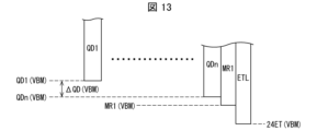
- FIG. 13 is a diagram showing the variation in the upper valence band levels QD1(VBM) to QDn(VBM) of the multiple quantum dots QD1 to QDn contained in the red light-emitting layer 24REM of the red light-emitting element 5R shown in FIG. 5 due to the variation in size and composition.
- the multiple quantum dots QD1 to QDn contained in the red light-emitting layer 24REM generally have a certain degree of variation ⁇ QD(VBM) in the upper valence band levels QD1(VBM) to QDn(VBM) of the quantum dots due to variations in size and composition.
- FIG. 14 shows the light emission energy distribution due to the variation in size and composition of quantum dots contained in the light emitting layers of each color in the red light emitting element 5R, green light emitting element 5G, and blue light emitting element 5B provided in the display device 1 of this embodiment.
- the emission spectrum of the red light-emitting layer 24REM provided in the red light-emitting element 5R when the emission peak wavelength (emission peak value) is 632 nm and the full width at half maximum (FWHM (full width half maximum)) is 38 nm, the energy fluctuation defined by the full width at half maximum of the emission peak value of the emission spectrum is 0.11 eV, which is the difference between the maximum value of 2.02 eV and the minimum value of 1.91 eV.
- the level MR1(VBM) of the upper end of the valence band of the matrix MR1 is preferably deeper than the level of the upper end of the valence band of the quantum dot calculated from the emission peak wavelength (emission peak value) of 632 nm plus 0.11 eV, and more preferably is deeper by 0.3 eV or more.
- the emission spectrum of the green light-emitting layer provided in the green light-emitting element 5G when the emission peak wavelength (emission peak value) is 532 nm and the full width at half maximum (FWHM (full width half maximum)) is 39 nm, the energy fluctuation defined by the full width at half maximum of the emission peak value of the emission spectrum is 0.17 eV, which is the difference between the maximum value of 2.42 eV and the minimum value of 2.25 eV.
- the level MR1(VBM) of the upper end of the valence band of the matrix MR1 is preferably deeper than the level of the upper end of the valence band of the quantum dot, which is deeper by adding 0.17 eV to the emission peak energy of the quantum dot calculated from the emission peak wavelength (emission peak value) of 532 nm, and is more preferably deeper by 0.3 eV or more.
- the energy fluctuation defined by the full width at half maximum of the emission peak value of the emission spectrum is 0.18 eV, which is the difference between the maximum value of 2.81 eV and the minimum value of 2.63 eV.
- the level MR1(VBM) of the upper end of the valence band of matrix MR1 is preferably deeper than the level of the upper end of the valence band of the quantum dot obtained by adding 0.18 eV to the emission peak energy of the quantum dot calculated from the emission peak wavelength (emission peak value) of 457 nm, and more preferably is deeper by 0.3 eV or more.
- Different matrix materials may be selected for the red light-emitting layer 24REM, the green light-emitting layer, and the blue light-emitting layer, but a matrix material may be selected to match the blue light-emitting layer, which has the greatest energy fluctuation.
- This disclosure can be used in light-emitting devices and display devices.
- Display device 3 Barrier layer 4 Thin film transistor layer 5R Red light emitting element (light emitting element) 5G green light-emitting element (light-emitting element) 5B Blue light-emitting element (light-emitting element) 12 Substrate 22 Anode 24R Functional layer including red light-emitting layer 24G Functional layer including green light-emitting layer 24B Functional layer including blue light-emitting layer 24REM Red light-emitting layer (light-emitting layer) 24HT Hole transport layer 24ET Electron transport layer 25 Cathode 30 Display panel 31 Scanning drive circuit 32 Data drive circuit PIX Pixel RSUB Red subpixel GSUB Green subpixel BSUB Blue subpixel DA Display area NDA Frame area QD Quantum dot CO Quantum dot core SH Quantum dot shell MR, MR1, MR2, MR3 Matrix MHa1, MHa2, MHa3 Metal halide CBM Conduction band bottom VBM Valence band top
Landscapes
- Engineering & Computer Science (AREA)
- Manufacturing & Machinery (AREA)
- Physics & Mathematics (AREA)
- Optics & Photonics (AREA)
- Chemical & Material Sciences (AREA)
- Crystallography & Structural Chemistry (AREA)
- Inorganic Chemistry (AREA)
- Nanotechnology (AREA)
- Materials Engineering (AREA)
- Electroluminescent Light Sources (AREA)
Abstract
発光素子(5R)は、アノード(22)と、カソード(25)と、アノード(22)とカソード(25)との間に設けられた赤色発光層(24REM)と、を備え、赤色発光層(24REM)は、複数の量子ドット(QD)と、複数の量子ドット(QD)それぞれの間の少なくとも一部に設けられたマトリクス(MR)とを含み、マトリクス(MR)は、金属ハロゲン化物(MHa1)を含むマトリクス(MR1)と、金属ハロゲン化物(MHa1)とは異なる金属ハロゲン化物(MHa2)を含むマトリクス(MR2)及び金属ハロゲン化物(MHa1)とは異なる金属ハロゲン化物(MHa3)を含むマトリクス(MR3)とを含み、マトリクス(MR1)は、マトリクス(MR2)及びマトリクス(MR3)よりもカソード(25)の近くに設けられている。
Description
本開示は、発光素子及び表示装置に関する。
近年、量子ドット含む発光素子であるQLED(Quantum dot Light Emitting Diode:量子ドット発光ダイオード)及びQLEDを備えた表示装置は、低消費電力化、薄型化及び高画質化などを実現できる点から、高い注目を浴びている。
例えば、特許文献1には、フッ素を含むナノ結晶粒子、すなわち、コア及びシェルの少なくとも一部にフッ素を含む量子ドットについて記載されている。
複数の量子ドットを含む発光層においては、複数の量子ドットそれぞれの間に存在する空間の影響により発光層の特性の低下が生じることが知られている。
特許文献1には、量子ドットのコア及びシェルの少なくとも一部が、例えば、金属フルオライド(fluoride)の形態で存在するフッ素を含むことについて記載されている。特許文献1に記載のフッ素を含む量子ドットの場合、量子ドットそのものの特性の改善は期待できるが、複数の量子ドットそれぞれの間に存在する空間の影響については言及されておらず、それによる発光層の特性に対する影響は依然問題として残っている。
そこで、本開示の発明者らは、発光層における複数の量子ドットそれぞれの間に存在する空間の少なくとも一部を埋めるマトリクスを用いることで発光層の特性の低下を抑制することを着想した。
さらに、本開示の発明者らは、金属硫化物であるZnSで構成される単一マトリクスまたは、金属硫化物であるZnSよりもバンドギャップが狭い材料で構成された単一マトリクスの場合、良好な発光特性が得られるとしても、以下のような更なる改善の余地があることを見出した。
金属硫化物であるZnSで構成される単一マトリクスを、発光層に含まれる量子ドットの発光効率を良好に維持するため、比較的低温工程で形成した場合、単一マトリクスは非発光再結合のパスとなり得る欠陥を含むこととなり、発光層において非発光リークが生じる。
一方で、上述した欠陥を減らすため、金属硫化物であるZnSで構成される単一マトリクスを数百度程度の比較的高温工程で形成した場合、発光層に含まれる量子ドットに影響を及ぼし、量子ドットの発光効率が低下することとなり得るので、発光層全体としては改善の余地がある。
また、金属硫化物であるZnSよりもバンドギャップが狭い材料で構成された単一マトリクスの場合、発光層に注入されたキャリアである正孔は、量子ドットを介さず前記単一マトリクスを伝導し、発光層と電子輸送層との界面まで到達し、発光層に注入されたキャリアである電子は、量子ドットを介さず前記単一マトリクスを伝導し、発光層と正孔輸送層との界面まで到達してしまうことによる、非発光再結合が上述した比較的高温工程で形成した結晶性の良いZnSで構成される単一マトリクスよりも起きやすく、発光層において非発光リークが生じ得るので、発光層全体としては改善の余地がある。
なお、前記単一マトリクスとは、一種類の化合物から構成されるマトリクスを意味する。
本開示の一態様は、さらに良好な発光効率及びさらに良好な非発光リークの抑制性を有する発光層を備えた発光素子と、前記発光素子を含む表示装置とを提供することを目的とする。
本開示の発光素子は、前記の課題を解決するために、
アノードと、
カソードと、
前記アノードと前記カソードとの間に設けられた発光層と、を備え、
前記発光層は、複数の量子ドットと、前記複数の量子ドットそれぞれの間の少なくとも一部に設けられたマトリクスとを含み、
前記マトリクスは、第1金属ハロゲン化物を含む第1部と、前記第1金属ハロゲン化物とは異なる第2金属ハロゲン化物を含む第2部とを含み、
前記第1部は、前記第2部よりも前記カソードの近くに設けられている。
アノードと、
カソードと、
前記アノードと前記カソードとの間に設けられた発光層と、を備え、
前記発光層は、複数の量子ドットと、前記複数の量子ドットそれぞれの間の少なくとも一部に設けられたマトリクスとを含み、
前記マトリクスは、第1金属ハロゲン化物を含む第1部と、前記第1金属ハロゲン化物とは異なる第2金属ハロゲン化物を含む第2部とを含み、
前記第1部は、前記第2部よりも前記カソードの近くに設けられている。
本開示の表示装置は、前記の課題を解決するために、
前記発光素子を含む。
前記発光素子を含む。
本開示の一態様によれば、さらに良好な発光効率及びさらに良好な非発光リークの抑制性を有する発光層を備えた発光素子と、前記発光素子を含む表示装置とを提供できる。
本開示の実施の形態について、図1から図14に基づいて説明すれば、次の通りである。以下、説明の便宜上、特定の実施形態にて説明した構成と同一の機能を有する構成については、同一の符号を付記し、その説明を省略する場合がある。
図1は、本実施形態の表示装置1の概略的な構成を示す平面図である。
図1に示すように、表示装置1は、表示パネル30を備えており、表示パネル30は、額縁領域NDAと、表示領域DAとを備えている。表示パネル30の表示領域DAには、複数の画素PIXが備えられており、各画素PIXは、それぞれ、赤色サブ画素RSUBと、緑色サブ画素GSUBと、青色サブ画素BSUBとを含む。本実施形態においては、1画素PIXが、赤色サブ画素RSUBと、緑色サブ画素GSUBと、青色サブ画素BSUBとで構成される場合を一例に挙げて説明するが、これに限定されることはない。例えば、1画素PIXは、赤色サブ画素RSUB、緑色サブ画素GSUB及び青色サブ画素BSUBの他に、さらに他の色のサブ画素を含んでいてもよい。また、本実施形態においては、表示パネル30の額縁領域NDAに、走査側駆動回路31と、データ側駆動回路32とが備えられている場合を一例に挙げて説明するが、これに限定されることはなく、走査側駆動回路31及びデータ側駆動回路32の少なくとも一方は、表示パネル30に外付けされていてもよい。
図2は、本実施形態の表示装置1に備えられた表示パネル30の表示領域DAの概略的な構成を示す断面図である。
図2に示すように、表示装置1に備えられた表示パネル30の表示領域DAにおいては、基板12上に、バリア層3と、トランジスタTRを含む薄膜トランジスタ層4と、赤色発光素子5R、緑色発光素子5G、青色発光素子5B及びバンク23と、封止層6と、機能フィルム39とが、基板12側からこの順に備えられている。
表示パネル30の表示領域DAに備えられた赤色サブ画素RSUBは赤色発光素子5Rを含み、表示パネル30の表示領域DAに備えられた緑色サブ画素GSUBは緑色発光素子5Gを含み、表示パネル30の表示領域DAに備えられた青色サブ画素BSUBは青色発光素子5Bを含む。
基板12は、例えば、ポリイミドなどの樹脂材料からなる樹脂基板であってもよく、ガラス基板であってもよい。本実施形態においては、表示装置1を可撓性表示装置とするため、基板12として、ポリイミドなどの樹脂材料からなる樹脂基板を用いた場合を一例に挙げて説明するが、これに限定されることはない。表示装置1を非可撓性表示装置とする場合には、基板12として、ガラス基板を用いることができる。
バリア層3は、水、酸素などの異物がトランジスタTR、赤色発光素子5R、緑色発光素子5G及び青色発光素子5Bに侵入することを防ぐ層であり、例えば、CVD法により形成される、酸化シリコン膜、窒化シリコン膜、あるいは酸窒化シリコン膜、またはこれらの積層膜で構成することができる。
トランジスタTRを含む薄膜トランジスタ層4のトランジスタTR部分は、半導体膜SEM及びドープされた半導体膜SEM’・SEM’’と、無機絶縁膜16と、ゲート電極Gと、無機絶縁膜18と、無機絶縁膜20と、ソース電極S及びドレイン電極Dと、平坦化膜21とを含み、トランジスタTRを含む薄膜トランジスタ層4のトランジスタTR部分以外の部分は、無機絶縁膜16と、無機絶縁膜18と、無機絶縁膜20と、平坦化膜21とを含む。
半導体膜SEM・SEM’・SEM’’は、例えば、低温ポリシリコン(LTPS)あるいは酸化物半導体(例えば、In-Ga-Zn-O系の半導体)で構成してもよい。本実施形態においては、トランジスタTRがトップゲート構造である場合を一例に挙げて説明するが、これに限定されることはなく、トランジスタTRは、ボトムゲート構造であってもよい。
ゲート電極Gと、ソース電極S及びドレイン電極Dとは、例えば、アルミニウム、タングステン、モリブデン、タンタル、クロム、チタン、銅の少なくとも1つを含む金属の単層膜あるいは積層膜によって構成できる。
無機絶縁膜16、無機絶縁膜18及び無機絶縁膜20は、例えば、CVD法によって形成された、酸化シリコン膜、窒化シリコン膜、酸窒化シリコン膜または、これらの積層膜によって構成することができる。
平坦化膜21は、例えば、ポリイミド、アクリルなどの塗布可能な有機材料によって構成することができるが、無機膜で形成してもよい。
赤色サブ画素RSUBに含まれる赤色発光素子5Rは、平坦化膜21よりも上層のアノード22と、赤色発光層を含む機能層24Rと、カソード25とを含み、緑色サブ画素GSUBに含まれる緑色発光素子5Gは、平坦化膜21よりも上層のアノード22と、緑色発光層を含む機能層24Gと、カソード25とを含み、青色サブ画素BSUBに含まれる青色発光素子5Bは、平坦化膜21よりも上層のアノード22と、青色発光層を含む機能層24Bと、カソード25とを含む。なお、アノード22のエッジを覆う絶縁性のバンク23は、例えば、ポリイミドまたはアクリルなどの有機材料を塗布した後にフォトリソグラフィー法によってパターニングすることで形成できるが、無機膜で形成してもよい。
本実施形態においては、赤色発光素子5R、緑色発光素子5G及び青色発光素子5Bが、順積構造である場合を一例に挙げて説明するが、これに限定されることはなく、赤色発光素子5R、緑色発光素子5G及び青色発光素子5Bは、逆積構造であってもよい。順積構造である赤色発光素子5R(図5参照)は、アノード22とアノード22よりも上層として備えられたカソード25とを備えており、アノード22とカソード25との間に備えられた赤色発光層24REMを含む機能層24Rは、例えば、アノード22側から順に、正孔注入層、正孔輸送層、赤色発光層、電子輸送層及び電子注入層を積層することで構成することができる。赤色発光層24REMを含む機能層24Rのうち、赤色発光層24REM以外の正孔注入層、正孔輸送層、電子輸送層及び電子注入層の1層以上を適宜省いてもよい。本実施形態においては、赤色発光層24REMを含む機能層24Rを、アノード22側から順に、正孔輸送層24HT、赤色発光層24REM及び電子輸送層24ETを積層することで構成した場合を一例に挙げて説明するが、これに限定されることはない。
順積構造である緑色発光素子5Gは、アノード22とアノード22よりも上層として備えられたカソード25とを備えており、アノード22とカソード25との間に備えられた緑色発光層を含む機能層24Gは、例えば、アノード22側から順に、正孔注入層、正孔輸送層、緑色発光層、電子輸送層及び電子注入層を積層することで構成することができる。緑色発光層を含む機能層24Gのうち、緑色発光層以外の正孔注入層、正孔輸送層、電子輸送層及び電子注入層の1層以上を適宜省いてもよい。本実施形態においては、緑色発光層を含む機能層24Gを、アノード22側から順に、正孔輸送層、緑色発光層及び電子輸送層を積層することで構成した場合を一例に挙げて説明するが、これに限定されることはない。
順積構造である青色発光素子5Bは、アノード22とアノード22よりも上層として備えられたカソード25とを備えており、アノード22とカソード25との間に備えられた青色発光層を含む機能層24Bは、例えば、アノード22側から順に、正孔注入層、正孔輸送層、青色発光層、電子輸送層及び電子注入層を積層することで構成することができる。青色発光層を含む機能層24Bのうち、青色発光層以外の正孔注入層、正孔輸送層、電子輸送層及び電子注入層の1層以上を適宜省いてもよい。本実施形態においては、青色発光層を含む機能層24Bを、アノード22側から順に、正孔輸送層、青色発光層及び電子輸送層を積層することで構成した場合を一例に挙げて説明するが、これに限定されることはない。
図示していない逆積構造である赤色発光素子は、カソードと前記カソードよりも上層として備えられたアノードとを備えており、前記カソードと前記アノードとの間に備えられた赤色発光層24REMを含む機能層は、例えば、前記カソード側から順に、電子注入層、電子輸送層、赤色発光層、正孔輸送層及び正孔注入層を積層することで構成することができる。赤色発光層24REMを含む機能層のうち、赤色発光層24REM以外の電子注入層、電子輸送層、正孔輸送層及び正孔注入層の1層以上を適宜省いてもよい。
図示していない逆積構造である緑色発光素子は、カソードと前記カソードよりも上層として備えられたアノードとを備えており、前記カソードと前記アノードとの間に備えられた緑色発光層を含む機能層は、例えば、前記カソード側から順に、電子注入層、電子輸送層、緑色発光層、正孔輸送層及び正孔注入層を積層することで構成することができる。前記緑色発光層を含む機能層のうち、緑色発光層以外の電子注入層、電子輸送層、正孔輸送層及び正孔注入層の1層以上を適宜省いてもよい。
図示していない逆積構造である青色発光素子は、カソードと前記カソードよりも上層として備えられたアノードとを備えており、前記カソードと前記アノードとの間に備えられた青色発光層を含む機能層は、例えば、前記カソード側から順に、電子注入層、電子輸送層、青色発光層、正孔輸送層及び正孔注入層を積層することで構成することができる。前記青色発光層を含む機能層のうち、青色発光層以外の電子注入層、電子輸送層、正孔輸送層及び正孔注入層の1層以上を適宜省いてもよい。
正孔注入層に用いられる材料としては、発光層内への正孔の注入を安定化させることができる正孔注入性材料であれば特に限定されるものではなく、例えば、ポリ(3,4-エチレンジオキシチオフェン)(PEDOT)とポリスチレンスルホン酸(PSS)との複合物(PEDOT:PSS)などを用いることができる。
正孔輸送層に用いられる材料としては、例えば、ポリ[(9,9-ジオクチルフルオレニル-2,7-ジイル)-co-(4,4’-(N-(4-sec-ブチルフェニル))ジフェニルアミン)](TFB)、N,N’-ビス(4-ブチルフェニル)-N,N’-ビス(フェニル)-ベンジジン(poly-TPD)またはポリビニルカルバゾール(PVK)などの有機材料を用いてもよく、NiO粒子などの正孔輸送性を有するナノ粒子を用いてもよい。
電子輸送層に用いられる材料としては、例えば、2,2′,2”-(1,3,5-ベンジントリイル)-トリス(1-フェニル-1-H-ベンズイミダゾール)(TPBi)などの有機材料を用いてもよく、ZnO粒子などの電子輸送性を有するナノ粒子を用いてもよい。
電子注入層に用いられる材料としては、発光層内への電子の注入を安定化させることができる電子注入性材料であれば特に限定されるものではなく、例えば、アルミニウム、ストロンチウム、カルシウム、リチウム、セシウム、酸化マグネシウム、酸化アルミニウム、酸化ストロンチウム、酸化リチウム、フッ化リチウム、フッ化マグネシウム、フッ化ストロンチウム、フッ化カルシウム、フッ化バリウム、フッ化セシウム、ポリメチルメタクリレートポリスチレンスルホン酸ナトリウムなどのようなアルカリ金属またはアルカリ土類金属、アルカリ金属またはアルカリ土類金属の酸化物、アルカリ金属またはアルカリ土類金属のフッ化物、アルカリ金属の有機錯体などを用いることができる。
また、本実施形態においては、赤色発光層24REMを含む機能層24R、緑色発光層を含む機能層24G及び青色発光層を含む機能層24Bのそれぞれが、同一材料を用いて同一工程で形成された正孔輸送層と、同一材料を用いて同一工程で形成された電子輸送層とを備えている場合を一例に挙げて説明するがこれに限定されることはない。例えば、各機能層24R・24G・24Bに含まれるそれぞれの正孔注入層を、同一材料を用いて同一工程で形成してもよく、互いに異なる材料で形成してもよく、機能層24R・24G・24Bのうちの2つの機能層のそれぞれに含まれる正孔注入層は同一材料を用いて同一工程で形成し、残りの1つの機能層に含まれる正孔注入層のみを異なる材料を用いて別工程で形成してもよい。また、例えば、各機能層24R・24G・24Bに含まれるそれぞれの正孔輸送層を、互いに異なる材料で形成してもよく、機能層24R・24G・24Bのうちの2つの機能層のそれぞれに含まれる正孔輸送層は同一材料を用いて同一工程で形成し、残りの1つの機能層に含まれる正孔輸送層のみを異なる材料を用いて別工程で形成してもよい。また、例えば、各機能層24R・24G・24Bに含まれるそれぞれの電子輸送層を、互いに異なる材料で形成してもよく、機能層24R・24G・24Bのうちの2つの機能層のそれぞれに含まれる電子輸送層は同一材料を用いて同一工程で形成し、残りの1つの機能層に含まれる電子輸送層のみを異なる材料を用いて別工程で形成してもよい。また、各機能層24R・24G・24Bに含まれるそれぞれの電子注入層を、同一材料を用いて同一工程で形成してもよく、互いに異なる材料で形成してもよく、機能層24R・24G・24Bのうちの2つの機能層のそれぞれに含まれる電子注入層は同一材料を用いて同一工程で形成し、残りの1つの機能層に含まれる電子注入層のみを異なる材料を用いて別工程で形成してもよい。
本実施形態においては、赤色発光素子5R、緑色発光素子5G及び青色発光素子5Bが、何れも、QLED(量子ドット発光ダイオード)である場合を一例に挙げて説明するが、これに限定されることはなく、赤色発光素子5R、緑色発光素子5G及び青色発光素子5Bのうちの1つ以上がQLEDであればよい。例えば、赤色発光素子5R、緑色発光素子5G及び青色発光素子5Bのうちの1つがQLEDである場合には、残りの2つがOLED(有機発光ダイオード)であってもよく、例えば、赤色発光素子5R、緑色発光素子5G及び青色発光素子5Bのうちの2つがQLEDである場合には、残りの1つがOLEDであってもよい。
本実施形態のように、赤色発光素子5R、緑色発光素子5G及び青色発光素子5Bのそれぞれが、QLEDである場合には、各色の発光素子が備えている発光層は量子ドットを含む。量子ドットは、例えば、コア構造、コア/シェル構造、コア/シェル/シェル構造、コア/比率を連続的に変化させたシェル構造を有してもよい。なお、シェルは、コアを完全に覆っていてもよいが、コアの一部分を覆っていてもよい。コア部は、一元系の場合、例えば、Si、Cなどで構成することができ、二元系の場合、例えば、CdSe、CdS、CdTe、InP、GaP、InN、ZnSe、ZnS、ZnTeなどで構成することができ、三元系の場合、例えば、CdSeTe、GaInP、ZnSeTeなどで構成することができ、四元系の場合、例えば、AIGSなどで構成することができる。シェル部は、二元系の場合、例えば、CdS、CdTe、CdSe、ZnS、ZnSe、ZnTeなどで構成することができ、三元系の場合、例えば、CdSSe、CdTeSe、CdSTe、ZnSSe、ZnSTe、ZnTeSe、AIPなどで構成することができる。
上述した量子ドットが、量子ドットの表面または量子ドットの表面の近傍に配置された有機リガンドまたは無機リガンド(例えば、ハロゲンリガンド)を含む場合には、量子ドットとは、有機リガンドまたは無機リガンド(例えば、ハロゲンリガンド)を含むものを意味する。
なお、前記量子ドットにおいて、リガンド部分を省いた最大幅は100nm以下である。また、前記量子ドットにおいて、リガンド部分を省いた形状は、上記最大幅を満たす範囲であればよく、特に制約されず、球状の立体形状(円状の断面形状)に限定されるものではない。例えば、多角形状の断面形状、棒状の立体形状、枝状の立体形状、表面に凹凸を有す立体形状でもよく、または、それらの組合せでもよい。
図2に示す赤色発光素子5R、緑色発光素子5G及び青色発光素子5Bは、トップエミッション型であっても、ボトムエミッション型であってもよい。赤色発光素子5R、緑色発光素子5G及び青色発光素子5Bは、アノード22よりもカソード25が上層として配置された順積構造であるので、トップエミッション型にするためには、アノード22は可視光を反射する電極材料で形成し、カソード25は可視光を透過する電極材料で形成すればよく、ボトムエミッション型にするためには、アノード22は可視光を透過する電極材料で形成し、カソード25は可視光を反射する電極材料で形成すればよい。一方、赤色発光素子、緑色発光素子及び青色発光素子が、カソード25よりもアノード22が上層として配置された逆積構造である場合、トップエミッション型にするためには、カソード25は可視光を反射する電極材料で形成し、アノード22は可視光を透過する電極材料で形成すればよく、ボトムエミッション型にするためには、カソード25は可視光を透過する電極材料で形成し、アノード22は可視光を反射する電極材料で形成すればよい。
可視光を反射する電極材料としては、可視光を反射でき、導電性を有するのであれば、特に限定されないが、例えば、Al、Mg、Li、Agなどの金属材料または、前記金属材料の合金または、前記金属材料と透明金属酸化物(例えば、indium tin oxide、indium zinc oxide、indium gallium zinc oxideなど)との積層体または、前記合金と前記透明金属酸化物との積層体などを挙げることができる。
一方、可視光を透過する電極材料としては、可視光を透過でき、導電性を有するのであれば、特に限定されないが、例えば、透明金属酸化物(例えば、indium tin oxide、indium zinc oxide、indium gallium zinc oxideなど)または、Al、Agなどの金属材料からなる薄膜または、Al、Agなどの金属材料からなるナノワイア(Nano Wire)などを挙げることができる。
アノード22及びカソード25の成膜方法としては、一般的な電極の形成方法を用いることができ、例えば、真空蒸着法、スパッタリング法、EB蒸着法、イオンプレーティング法などの物理的蒸着(PVD)法、あるいは、化学的蒸着(CVD)法などを挙げることができる。また、アノード22及びカソード25のパターニング方法としては、所望のパターンに精度よく形成することができる方法であれば特に限定されるものではないが、具体的にはフォトリソグラフィー法やインクジェット法などを挙げることができる。
封止層6は透光性膜であり、例えば、カソード25を覆う無機封止膜26と、無機封止膜26よりも上層の有機膜27と、有機膜27よりも上層の無機封止膜28とで構成することができる。封止層6は、水、酸素などの異物の赤色発光素子5R、緑色発光素子5G及び青色発光素子5Bへの浸透を防いでいる。
無機封止膜26及び無機封止膜28はそれぞれ無機膜であり、例えば、CVD法により形成される、酸化シリコン膜、窒化シリコン膜、あるいは酸窒化シリコン膜、またはこれらの積層膜で構成することができる。有機膜27は、平坦化効果のある透光性有機膜であり、例えば、アクリルなどの塗布可能な有機材料によって構成することができる。有機膜27は、例えばインクジェット法によって形成してもよい。本実施形態においては、封止層6を、2層の無機膜と2層の無機膜の間に設けられた1層の有機膜とで形成した場合を一例に挙げて説明したが、2層の無機膜と1層の有機膜の積層順はこれに限定されることはない。さらに、封止層6は、無機膜のみで構成されてもよく、有機膜のみで構成されてもよく、1層の無機膜と2層の有機膜とで構成されてもよく、2層以上の無機膜と2層以上の有機膜とで構成されてもよい。
機能フィルム39は、例えば、光学補償機能、タッチセンサ機能、保護機能の少なくとも1つを有するフィルムである。
複数の量子ドットQDを含む発光層においては、複数の量子ドットQDそれぞれの間に存在する空間の影響により発光層の特性の低下が生じることが知られている。
本開示の発明者らは、発光層における複数の量子ドットQDそれぞれの間に存在する空間の少なくとも一部を埋めるマトリクスを用いることで発光層の特性の低下を抑制することを着想した。
発光層における複数の量子ドットQDそれぞれの間に存在する空間の少なくとも一部を埋めるマトリクスが、金属硫化物であるZnSで構成される単一マトリクスである場合、前記単一マトリクスを、発光層に含まれる量子ドットの発光効率を良好に維持するため、比較的低温工程(例えば、25℃以上、100℃以下)で形成した場合、前記単一マトリクスは非発光再結合のパスとなり得る欠陥を含むこととなり、発光層において非発光リークが生じる。一方、上述した欠陥を減らすため、金属硫化物であるZnSで構成される単一マトリクスを数百度程度の比較的高温工程で形成した場合、発光層に含まれる量子ドットに影響を及ぼし、量子ドットの発光効率が低下することとなり得る。したがって、金属硫化物であるZnSで構成される単一マトリクスを含む発光層の場合、良好な発光特性が得られるとしても、発光層全体としては改善の余地がある。
そこで、本開示の発明者らは、後述する比較例である赤色発光素子5Rrのように、単一マトリクスMRrをヨウ化銅(CuI)またはヨウ化銀(AgI)のような金属ハロゲン化物MHaで構成することで、単一マトリクスMRrを金属硫化物であるZnSで構成した場合と比較して、良好な発光効率及び良好な非発光リークの抑制性を有する発光層を備えた発光素子を実現できることを見出した。
後述する比較例である赤色発光素子5Rrのように、単一マトリクスMRrをヨウ化銅(CuI)またはヨウ化銀(AgI)のような金属ハロゲン化物MHaで構成した場合、比較的低温(例えば、25℃以上、100℃以下)である、例えば、室温でも高結晶性の単一マトリクスMRrを生成することができるので、良好な発光効率及び良好な非発光リークの抑制性を有する発光層を実現できる。なお、前記単一マトリクスとは、一種類の化合物から構成されるマトリクスを意味する。
図3は、比較例である赤色発光素子5Rrの概略的な構成を示す断面図である。
図3に示す符号の最後に小文字の「r」を付けている構成は、後述する本実施形態の構成とは異なる比較例の構成を意味する。比較例である赤色発光素子5Rrは、金属ハロゲン化物MHaで構成された単一マトリクスMRrを備えている赤色発光層24REMrを含む機能層24Rrを含む構成であり、後述する図5に示す本実施形態の赤色発光素子5Rの構成とは異なる。
図3に示すように、赤色発光素子5Rrは、アノード22と、カソード25と、アノード22とカソード25との間に設けられた赤色発光層24REMrを含む機能層24Rrとを備えている。赤色発光層24REMrを含む機能層24Rrは、アノード22側から順に、正孔輸送層24HTと、赤色発光層24REMrと、電子輸送層24ETとが積層されて構成されている。
赤色発光層24REMrは、コアCO及びシェルSHを含む複数の量子ドットQDと、複数の量子ドットQDそれぞれの間に存在する空間を充填するように設けられた金属元素とハロゲン元素とからなる金属ハロゲン化物MHaで構成された単一マトリクスMRrとを含む。ここでは、比較例である赤色発光素子5Rrに備えられた単一マトリクスMRrを構成する金属ハロゲン化物MHaが、例えば、金属元素である銅(Cu)とハロゲン元素であるヨウ素(I)とからなるヨウ化銅(CuI)である場合を一例に挙げて説明するが、これに限定されることはなく、単一マトリクスMRrを構成する金属ハロゲン化物MHaは、金属元素である銀(Ag)とハロゲン元素であるヨウ素(I)とからなるヨウ化銀(AgI)であってもよい。なお、単一マトリクスMRrを構成する金属ハロゲン化物MHaは、金属硫化物であるZnSよりもバンドギャップが狭い材料である。
図4は、図3に示した比較例である赤色発光素子5Rrに備えられた、電子輸送層24ETと、赤色発光層24REMrに含まれる量子ドットQDと、赤色発光層24REMrに含まれる単一マトリクスMRrとのバンド準位を概略的に示す図である。
本開示の発明者らは、上述した比較例である赤色発光素子5Rrのように、単一マトリクスMRrをヨウ化銅(CuI)またはヨウ化銀(AgI)のような金属ハロゲン化物MHaで構成した場合に、図4に示すように、量子ドットQDの価電子帯上端の準位QD(VBM)と単一マトリクスMRrの価電子帯上端の準位MRr(VBM)とが近くなるとともに、量子ドットQDのバンドギャップと単一マトリクスMRrのバンドギャップとも近くなることを見出した。
例えば、赤色を発光する量子ドットQDのバンドギャップは2.0eVであり、緑色を発光する量子ドットQDのバンドギャップは2.3eVであり、青色を発光する量子ドットQDのバンドギャップは2.8eVである。
したがって、バンドギャップが3.8eVである金属硫化物であるZnSの代わりに、バンドギャップは3.1eVであるヨウ化銅(CuI)を用いて単一マトリクスMRrを構成した場合、上述したように、量子ドットQDの価電子帯上端の準位QD(VBM)と単一マトリクスMRrの価電子帯上端の準位MRr(VBM)とが近くなるとともに、量子ドットQDのバンドギャップと単一マトリクスMRrのバンドギャップとも近くなる。
このような場合、図4に示すように、赤色発光層24REMrに注入されたキャリアである正孔Hが、量子ドットQDを介さず単一マトリクスMRrを伝導し、赤色発光層24REMrと電子輸送層24ETとの界面まで到達してしまうことによる、非発光再結合が上述した比較的高温工程で形成した結晶性の良いZnSで構成される単一マトリクスよりも起きやすく、赤色発光層24REMrにおいて非発光リークが生じ得るので、赤色発光層24REMr全体としては改善の余地がある。
そこで、本開示の発明者らは、さらに良好な発光効率及びさらに良好な非発光リークの抑制性を有する発光層を備えた発光素子と、前記発光素子を含む表示装置を提案する。
図5は、本実施形態の表示装置1に備えられた赤色発光素子5Rの概略的な構成を示す断面図である。
図6は、図5に示した赤色発光素子5Rに備えられた、電子輸送層24ETと、赤色発光層24REMに含まれる量子ドットQDと、赤色発光層24REMに含まれるマトリクスMRとのバンド準位を概略的に示す図である。
図5に示すように、表示装置1に備えられた赤色発光素子5Rは、アノード22と、カソード25と、アノード22とカソード25との間に設けられた赤色発光層24REMと、を備えている。
赤色発光層24REMを含む機能層24Rは、アノード22側から順に、正孔輸送層24HTと、赤色発光層24REMと、電子輸送層24ETとが積層されて構成されている。
赤色発光層24REMは、コアCO及びシェルSHを含む複数の量子ドットQDと、複数の量子ドットQDそれぞれの間の少なくとも一部に設けられた金属元素とハロゲン元素とからなる複数の金属ハロゲン化物MHa1・MHa2・MHa3を含むマトリクスMRとを含む。本実施形態においては、発光効率及び非発光リークの抑制性をさらに高める効果を得るため、図5に示すように、マトリクスMRが、複数の量子ドットQDそれぞれの間に存在する空間を充填するように設けた場合を一例に挙げて説明するが、これに限定されることはなく、マトリクスMRが、複数の量子ドットQDそれぞれの間に存在する空間の一部に設けられていても、発光効率及び非発光リークの抑制性を高める効果を得ることはできる。
マトリクスMRは、第1金属ハロゲン化物を含む第1部と、前記第1金属ハロゲン化物とは異なる第2金属ハロゲン化物を含む第2部とを含み、前記第1部は、前記第2部よりもカソード25の近くに設けられている。
図5に示す赤色発光素子5Rに備えられた赤色発光層24REMの場合、第1金属ハロゲン化物を含む第1部が前記第1金属ハロゲン化物とは異なる第2金属ハロゲン化物を含む第2部よりもカソード25の近くに設けられていればよいので、例えば、金属ハロゲン化物MHa1を含むマトリクスMR1を第1部とした場合、金属ハロゲン化物MHa2を含むマトリクスMR2及び金属ハロゲン化物MHa3を含むマトリクスMR3の少なくとも一方が第2部となり、金属ハロゲン化物MHa2を含むマトリクスMR2を第1部とした場合、金属ハロゲン化物MHa3を含むマトリクスMR3が第2部となる。図5に示す赤色発光素子5Rに備えられた赤色発光層24REMに含まれるマトリクスMRは、異なる二種類以上の化合物である、金属ハロゲン化物MHa1、金属ハロゲン化物MHa2及び金属ハロゲン化物MHa3で構成されているので、上述した比較例である赤色発光素子5Rrに備えられた一種類の化合物である一種類の金属ハロゲン化物MHaで構成された単一マトリクスMRrとは異なる。なお、異なる化合物とは、異なる元素から構成される化合物を含むことは勿論、同一元素から構成される化合物であっても組成比が異なる化合物も含むものである。
図4に示すように、上述した比較例である赤色発光素子5Rrの場合、単一マトリクスMRrをヨウ化銅(CuI)またはヨウ化銀(AgI)のような一種類の化合物である一種類の金属ハロゲン化物MHaで構成しているので、単一マトリクスMRrの価電子帯上端の準位MRr(VBM)及び単一マトリクスMRrの伝導帯下端の準位MRr(CBM)のそれぞれは、一つの量子準位となるので、赤色発光層24REMrに注入されたキャリアである正孔Hは、単一マトリクスMRrの価電子帯上端の準位MRr(VBM)を素通りし、赤色発光層24REMrと電子輸送層24ETとの界面まで到達し、赤色発光層24REMrに注入されたキャリアである電子Eは、単一マトリクスMRrの伝導帯下端の準位MRr(CBM)を素通りし、赤色発光層24REMrと正孔輸送層24HTとの界面まで到達してしまい、非発光再結合が起きやすいことから、赤色発光層24REMrにおいて非発光リークが生じ得るので、赤色発光層24REMr全体としては改善の余地があった。
一方、図5に示す本実施形態の赤色発光素子5Rの場合、マトリクスMRが、第1金属ハロゲン化物を含む第1部と、前記第1金属ハロゲン化物とは異なる第2金属ハロゲン化物を含む第2部とを含むので、図6に示すように、マトリクスMRの価電子帯上端の準位及びマトリクスMRの伝導帯下端の準位のそれぞれは、複数の異なる量子準位となるので、赤色発光層24REMに注入されたキャリアである正孔Hは、マトリクスMRの価電子帯上端の準位を素通りできず、赤色発光層24REMと電子輸送層24ETとの界面まで到達するのが抑制され、赤色発光層24REMに注入されたキャリアである電子Eは、マトリクスMRの伝導帯下端の準位を素通りできず、赤色発光層24REMと正孔輸送層24HTとの界面まで到達するのが抑制され、非発光再結合を抑制できるので、赤色発光層24REMにおいてさらに良好な発光効率及びさらに良好な非発光リークの抑制性を得ることができる。
前記第2部よりもカソード25の近くに設けられている第1部の価電子帯上端の準位は、前記第2部の価電子帯上端の準位よりも深いことが好ましい。そこで、図6に示すように、本実施形態の赤色発光素子5Rにおいては、金属ハロゲン化物MHa2を含むマトリクスMR2と金属ハロゲン化物MHa3を含むマトリクスMR3とが積層された部分の価電子帯上端の準位MR2&3(VBM)は、金属ハロゲン化物MHa3を含むマトリクスMR3の価電子帯上端の準位MR3(VBM)よりも深く、金属ハロゲン化物MHa1を含むマトリクスMR1と金属ハロゲン化物MHa2を含むマトリクスMR2とが積層された部分の価電子帯上端の準位MR1&2(VBM)は、金属ハロゲン化物MHa2を含むマトリクスMR2と金属ハロゲン化物MHa3を含むマトリクスMR3とが積層された部分の価電子帯上端の準位MR2&3(VBM)よりも深く、金属ハロゲン化物MHa1を含むマトリクスMR1の価電子帯上端の準位MR1(VBM)は、金属ハロゲン化物MHa1を含むマトリクスMR1と金属ハロゲン化物MHa2を含むマトリクスMR2とが積層された部分の価電子帯上端の準位MR1&2(VBM)よりも深くなっている。
本実施形態の赤色発光素子5Rによれば、図6に示すように、注入されたキャリアである正孔Hが階段状のポテンシャルを通ることとなり、正孔Hが赤色発光層24REM内を進むにつれ通るのが難しくなるため、正孔Hが赤色発光層24REMと電子輸送層24ETとの界面まで到達するのが抑制され、非発光再結合を抑制できるとともに、正孔Hと電子Eの再結合が起きる位置を赤色発光層24REMの厚さ方向の中心位置にすることができる。したがって、赤色発光層24REMにおいてさらに良好な発光効率及びさらに良好な非発光リークの抑制性を得ることができる。
また、前記第2部よりもカソード25の近くに設けられている第1部の伝導帯下端の準位は、前記第2部の伝導帯下端の準位よりも深いことが好ましい。そこで、図6に示すように、本実施形態の赤色発光素子5Rにおいては、金属ハロゲン化物MHa2を含むマトリクスMR2と金属ハロゲン化物MHa3を含むマトリクスMR3とが積層された部分の伝導帯下端の準位MR2&3(CBM)は、金属ハロゲン化物MHa3を含むマトリクスMR3の伝導帯下端の準位MR3(CBM)よりも深く、金属ハロゲン化物MHa1を含むマトリクスMR1と金属ハロゲン化物MHa2を含むマトリクスMR2とが積層された部分の伝導帯下端の準位MR1&2(CBM)は、金属ハロゲン化物MHa2を含むマトリクスMR2と金属ハロゲン化物MHa3を含むマトリクスMR3とが積層された部分の伝導帯下端の準位MR2&3(CBM)よりも深く、金属ハロゲン化物MHa1を含むマトリクスMR1の伝導帯下端の準位MR1(CBM)は、金属ハロゲン化物MHa1を含むマトリクスMR1と金属ハロゲン化物MHa2を含むマトリクスMR2とが積層された部分の伝導帯下端の準位MR1&2(CBM)よりも深くなっている。
本実施形態の赤色発光素子5Rによれば、図6に示すように、注入されたキャリアである電子Eが階段状のポテンシャルを通ることとなり、電子Eが赤色発光層24REM内を進むにつれ通るのが難しくなるため、電子Eが赤色発光層24REMと正孔輸送層24HTとの界面まで到達するのが抑制され、非発光再結合を抑制できるとともに、正孔Hと電子Eの再結合が起きる位置を赤色発光層24REMの厚さ方向の中心位置にすることができる。したがって、赤色発光層24REMにおいてさらに良好な発光効率及びさらに良好な非発光リークの抑制性を得ることができる。
図5に示すように、本実施形態の赤色発光素子5Rにおいては、マトリクスMR1に含まれる金属ハロゲン化物MHa1と、マトリクスMR2に含まれる金属ハロゲン化物MHa2と、マトリクスMR3に含まれる金属ハロゲン化物MHa3とのそれぞれが、組成比が異なるヨウ化銅である場合を一例に挙げて説明するが、これに限定されることはなく、例えば、組成比が異なるヨウ化銀であってもよい。本実施形態においては、金属ハロゲン化物MHa1、金属ハロゲン化物MHa2及び金属ハロゲン化物MHa3のそれぞれが、同一元素から構成される化合物であって、組成比が異なる化合物である場合を一例に挙げて説明したが、これに限定されることはなく、異なる元素から構成される化合物であってもよい。また、本実施形態においては、マトリクスMRに含まれる各マトリクス単位で同一元素から構成される化合物の組成比が異なる場合を一例に挙げて説明したが、これに限定されることはなく、マトリクスMRに含まれるある一つのマトリクスが異なる二種類以上の化合物で構成されていてもよく、マトリクスMRに含まれるある一つのマトリクスが、厚さ方向においてその組成比が連続的に変わる化合物で構成されていてもよい。なお、本実施形態においては、マトリクスMRが、マトリクスMR1とマトリクスMR2とマトリクスMR3とで構成されている場合を一例に挙げて説明するがこれに限定されることはなく、マトリクスMRは、例えば、マトリクスMR1とマトリクスMR2とで構成されていてもよく、4つ以上の異なるマトリクスで構成されていてもよい。
本実施形態の赤色発光素子5Rにおいては、マトリクスMR1に含まれる金属ハロゲン化物MHa1の(金属元素/ハロゲン元素)の比の値が、マトリクスMR2に含まれる金属ハロゲン化物MHa2の(金属元素/ハロゲン元素)の比の値及びマトリクスMR3に含まれる金属ハロゲン化物MHa3の(金属元素/ハロゲン元素)の比の値よりも小さくなっており、マトリクスMR1に含まれるヨウ化銅の(銅元素/ヨウ素元素)の比の値が、マトリクスMR2に含まれるヨウ化銅の(銅元素/ヨウ素元素)の比の値及びマトリクスMR3に含まれるヨウ化銅の(銅元素/ヨウ素元素)の比の値よりも小さくなっている。すなわち、マトリクスMR2及びマトリクスMR3に含まれるヨウ化銅は、P型のヨウ化銅となっており、マトリクスMR1に含まれるヨウ化銅は、真性に近いヨウ化銅となっている。
なお、(金属元素/ハロゲン元素)の比の値とは、該当するマトリクス、例えば、マトリクスMR1、マトリクスMR2及びマトリクスMR3それぞれに含まれる化合物における金属元素とハロゲン元素との比の値である。
上述したように、本実施形態においては、マトリクスMR1よりもアノード22の近くに設けられたマトリクスMR2及びマトリクスMR3において、正孔Hの移動度が高いP型のヨウ化銅を用いているので、例えば、電子輸送層24ETとして、電子の移動度が高いZnO粒子などが用いられた場合においても、正孔Hと電子Eとのキャリアバランスを改善することができる。
上述したマトリクスMR1に含まれるヨウ化銅のキャリア密度(正孔Hのキャリア密度)は、1×1015cm-3以上、1×1019cm-3以下であることが好ましく、上述したマトリクスMR1に含まれるヨウ化銅の(銅元素/ヨウ素元素)の比の値は、例えば、0.95以上、1.0以下で適宜決めることが好ましい。マトリクスMR2及びマトリクスMR3よりもカソード25の近くに設けられたマトリクスMR1に含まれるヨウ化銅は、ストイキオメトリ(化学量論比)的に1:1である真性に近い(銅元素/ヨウ素元素)の比を有することが好ましい。
上述したマトリクスMR2及びマトリクスMR3に含まれるヨウ化銅のキャリア密度(正孔Hのキャリア密度)は、1×1018cm-3以上、1×1020cm-3以下であることが好ましく、上述したマトリクスMR2及びマトリクスMR3に含まれるヨウ化銅の(銅元素/ヨウ素元素)の比の値は、例えば、0.5以上、0.99以下で適宜決めることが好ましい。
本実施形態の赤色発光素子5Rにおいては、上述したマトリクスMR1に含まれるヨウ化銅の(銅元素/ヨウ素元素)の比の値は0.95に、上述したマトリクスMR2に含まれるヨウ化銅の(銅元素/ヨウ素元素)の比の値は0.97に、上述したマトリクスMR3に含まれるヨウ化銅の(銅元素/ヨウ素元素)の比の値は0.99にした場合を一例に挙げて説明するが、これに限定されることはない。
本実施形態の赤色発光素子5Rにおいては、赤色発光層24REMに注入されたキャリアである正孔Hが、量子ドットQDを介さずマトリクスMRを伝導し、赤色発光層24REMと電子輸送層24ETとの界面まで到達してしまうのを抑制するため、図6に示すように、少なくとも、マトリクスMR1の価電子帯上端の準位MR1(VBM)が量子ドットQDの価電子帯上端の準位QD(VBM)よりも深くなるようにしているが、これに限定されることはない。
さらに、マトリクスMR1の価電子帯上端の準位MR1(VBM)が量子ドットQDの価電子帯上端の準位QD(VBM)よりも0.3eV以上深くなるようにすることで、赤色発光層24REMに注入されたキャリアである正孔Hが、量子ドットQDを介さずマトリクスMRを伝導し、赤色発光層24REMと電子輸送層24ETとの界面まで到達してしまうのをより抑制することができる。
本実施形態においては、マトリクスMR1に含まれる金属ハロゲン化物MHa1、マトリクスMR2に含まれる金属ハロゲン化物MHa2及びマトリクスMR3に含まれる金属ハロゲン化物MHa3のそれぞれが、上述したように、1種類の金属元素(銅元素または銀元素)を含む場合を一例に挙げて説明したが、これに限定されることはなく、マトリクスMR1に含まれる金属ハロゲン化物MHa1、マトリクスMR2に含まれる金属ハロゲン化物MHa2及びマトリクスMR3に含まれる金属ハロゲン化物MHa3の少なくとも一つは、2種類以上の金属元素を含んでいてもよい。
マトリクスMR1に含まれる金属ハロゲン化物MHa1、マトリクスMR2に含まれる金属ハロゲン化物MHa2及びマトリクスMR3に含まれる金属ハロゲン化物MHa3のそれぞれは、金属元素として、少なくとも第1金属元素及び第2金属元素を含んでいてもよい。
例えば、CuまたはAgを前記第1金属元素とし、N型のドーパント金属元素であるZn、Cd、Sn、Ti、Zr、Ta及びWの中から選択された一つの金属元素を前記第2金属元素としてもよい。
以上のように、N型のドーパント金属元素である第2金属元素をさらに用いることで、マトリクスのバンド及びフェルミ準位をより幅広く制御することができる。
マトリクスMR1に含まれる金属ハロゲン化物MHa1の(前記第2金属元素/前記第1金属元素)の比の値は、マトリクスMR2に含まれる金属ハロゲン化物MHa2及びマトリクスMR3に含まれる金属ハロゲン化物MHa3の(前記第2金属元素/前記第1金属元素)の比の値よりも大きいことが好ましい。
例えば、マトリクスMR1に含まれる金属ハロゲン化物MHa1は、銅(Cu)と亜鉛(Zn)とヨウ素(I)とが第1の組成比で構成され、マトリクスMR2に含まれる金属ハロゲン化物MHa2は、銅(Cu)と亜鉛(Zn)とヨウ素(I)とが前記第1の組成比とは異なる第2の組成比で構成され、マトリクスMR3に含まれる金属ハロゲン化物MHa3は、銅(Cu)と亜鉛(Zn)とヨウ素(I)とが前記第1の組成比及び前記第2の組成比とは異なる第3の組成比で構成されていてもよい。
上述したように、マトリクスMR1に含まれる金属ハロゲン化物MHa1が、銅(Cu)と亜鉛(Zn)とヨウ素(I)とで構成されている場合には、マトリクスMR1に含まれる金属ハロゲン化物MHa1のキャリア密度は、1×1015cm-3以上、1×1019cm-3以下であることが好ましく、マトリクスMR1に含まれる金属ハロゲン化物MHa1の(銅元素/ヨウ素元素)の比の値は、0.95以上、1.0以下で、マトリクスMR1に含まれる金属ハロゲン化物MHa1の(亜鉛元素/銅元素)の比の値は、0.01以上、0.5以下で適宜決めることが好ましい。
上述したように、マトリクスMR2に含まれる金属ハロゲン化物MHa2及びマトリクスMR3に含まれる金属ハロゲン化物MHa3のそれぞれが、銅(Cu)と亜鉛(Zn)とヨウ素(I)とで構成されている場合には、マトリクスMR2に含まれる金属ハロゲン化物MHa2及びマトリクスMR3に含まれる金属ハロゲン化物MHa3のキャリア密度は、1×1018cm-3以上、1×1020cm-3以下であることが好ましく、金属ハロゲン化物MHa2及び金属ハロゲン化物MHa3の(銅元素/ヨウ素元素)の比の値は、0.5以上、0.99以下で、金属ハロゲン化物MHa2及び金属ハロゲン化物MHa3の(亜鉛元素/銅元素)の比の値は、1×10-11以上、0.01以下で適宜決めることが好ましい。
本実施形態においては、図5に示すように、複数の量子ドットQDそれぞれがマトリクスMRに埋め込まれている、すなわち、マトリクスMRが複数の量子ドットQDそれぞれを囲み込んでいる場合を一例に挙げて説明するが、これに限定されることはなく、マトリクスMRは、複数の量子ドットQDそれぞれの間の少なくとも一部に設けられていればよい。
図7は、図5に示した赤色発光素子5Rに備えられた赤色発光層24REMに含まれる複数の量子ドットQDのうち、隣り合う2つの量子ドットQD1・QD2が近づいて配置されている場合において、量子ドットQD1・QD2の間に形成される領域Rを説明するための図である。
図8は、図5に示した赤色発光素子5Rに備えられた赤色発光層24REMに含まれる複数の量子ドットQDのうち、隣り合う2つの量子ドットQD1・QD2が少し離れて配置されている場合において、量子ドットQD1・QD2の間に形成される領域Rを説明するための図である。
図7及び図8に示す領域Rは、隣り合う2つの量子ドットQD1・QD2の外周に接する二つの直線(共通外接線)と、隣り合う2つの量子ドットQD1・QD2の対向する外周とに囲まれた領域である。図7に示すように、隣り合う2つの量子ドットQD1・QD2が近づいて配置されている場合でも、図8に示すように、隣り合う2つの量子ドットQD1・QD2が少し離れて配置されている場合でも、領域Rは存在し、領域RはマトリクスMRで充填されている。「隣り合う2つの量子ドットQD1・QD2の間にマトリクスMRが充填されている」とは、図7及び図8に示す領域RにマトリクスMRが充填されているまたは充たされていることを意味する。なお、本開示においては、領域RにマトリクスMRが存在することにより隣り合う2つの量子ドットQD1・QD2が保持されていてもよく、例えば、領域Rの少なくとも一部がマトリクスMRで充填されていてもよい。
本実施形態においては、図7及び図8に示す隣り合う2つの量子ドットQD1・QD2の間に形成される領域R、すなわち、複数の量子ドットQDの間の空間は、マトリクスMRで充填されている場合を一例に挙げて説明するが、これに限定されることはない。
なお、隣り合う2つの量子ドットQD1・QD2の間に形成される領域Rに存在するマトリクスMRによって量子ドットQD1・QD2が保持されているとは、領域Rの少なくとも一部がマトリクスMRで埋められていることを意味し、領域R全体をマトリクスMRが満たしている場合は勿論、領域Rの一部をマトリクスMRが満たしている場合も含む意味である。
マトリクスMRは、発光層の複数の量子ドットQD以外の領域(空間)を埋めるように形成されていてもよい。また、図5に示すように、マトリクスMRが発光層(例えば、赤色発光層24REM)の外縁を構成し、複数の量子ドットQDは前記外縁から離れて位置するように構成してもよい。すなわち、マトリクスMRが複数の量子ドットQDを内包していてもよい。さらに、発光層の外縁の少なくとも一部は、マトリクスMRと量子ドットQDとで構成されていてもよい。また、複数の量子ドットQDのそれぞれは、マトリクスMRに間隔を置いて埋設されていてもよい。なお、ここで外縁とは、発光層の第1面(例えば、図5に示す赤色発光層24REMの電子輸送層24ETと接する面)及び発光層の第2面(例えば、図5に示す赤色発光層24REMの正孔輸送層24HTと接する面)を意味する。
マトリクスMRは、連続膜を含んでいてもよい。連続膜とは、連続膜を構成する材料以外の材料で分断されない膜を意味する。連続膜は、マトリクスMRに含まれる金属ハロゲン化物MHa1・MHa2・MHa3の化学結合によって途切れることなく連結した一体の膜状のものであってもよい。
「複数の量子ドットQDそれぞれの間の少なくとも一部にマトリクスMRが設けられている」とは、少なくとも2つの量子ドットQDの間にマトリクスMRが充填されていることが分かれば足る。
なお、「複数の量子ドットQD間にマトリクスMRが充填されている」場合、すなわち、少なくとも1つの「隣り合う2つの量子ドットQD1・QD2の間にマトリクスMRが充填されている」ことが確認できた場合が、その量子ドットQD間においてマトリクスMRが最も多く存在することができているので、その量子ドットQD間におけるマトリクスMRが奏する効果が最も高く働くため、非常に高い効果を奏することができ、望ましい。
図9は、図5に示した赤色発光素子5Rに備えられた赤色発光層24REMを形成する工程の一例を示す図である。
図10は、図9に示した赤色発光層24REMを形成する工程を説明するための図である。
図9及び図10に示すように、複数の量子ドットQDと、金属ハロゲン化物MHa1を含むマトリクスMR1と、金属ハロゲン化物MHa2を含むマトリクスMR2と、金属ハロゲン化物MHa3を含むマトリクスMR3とを含む赤色発光層24REMは、SILAR法(Successive ionic layer adsorption and reaction)のような溶液法により例えば、25℃以上、100℃以下において形成が可能である。
赤色発光素子5Rに備えられた赤色発光層24REMを形成する工程は、基板上(例えば、基板上に設けられた正孔輸送層24HT上)に複数の量子ドットQDを含む所定の厚さの量子ドット層を形成する工程(図9及び図10のS1工程)と、前記量子ドット層に対して、前記金属元素(例えば、Cu)のイオン及び前記ハロゲン元素(例えば、I)のイオンの一方を含む第1溶液を用いて処理を行う第1溶液処理工程と、前記第1溶液処理工程の後に、前記量子ドット層に対して、前記金属元素(例えば、Cu)のイオン及び前記ハロゲン元素(例えば、I)のイオンの他方を含む第2溶液を用いて処理を行う第2溶液処理工程と、を含む。
本実施形態の前記第1溶液処理工程(図9のS2工程)においては、前記金属元素(例えば、Cu)のイオン源となる溶液(例えば、0.1mol/lの[Cu(S2O3)]錯体溶液)を、前記量子ドット層に対して、塗布して量子ドットQD表面へのCuイオンの吸着を行ってもよく、前記量子ドット層を前記金属元素(例えば、Cu)のイオン源となる溶液に浸漬させて量子ドットQD表面へのCuイオンの吸着を行ってもよい。
その後、必要に応じて余剰Cuイオンを除去するリンス工程(図9及び図10のS3工程)を行ってもよい。
それから、本実施形態の前記第2溶液処理工程(図9のS4工程)においては、前記ハロゲン元素(例えば、I)のイオン源となる溶液(例えば、0.025mol/lのKI溶液)を、前記量子ドット層に対して、塗布して量子ドットQD表面へのIイオンの吸着を行い、Cuイオンと反応させてもよく、前記量子ドット層を前記ハロゲン元素(例えば、I)のイオン源となる溶液に浸漬させて量子ドットQD表面へのIイオンの吸着を行い、Cuイオンと反応させてもよい。
なお、前記第2溶液処理工程(図9のS4工程)においては、マトリクスMR3に含まれるヨウ化銅の(銅元素/ヨウ素元素)の比の値が0.99となるように、Iのイオン源となる溶液の使用量を調整する。
その後、必要に応じて余剰Iイオンを除去するリンス工程(図9及び図10のS5工程)を行ってもよい。
以上により、金属ハロゲン化物MHa3であるヨウ化銅を含むマトリクスMR3へ埋め込まれた量子ドットQDを含む発光層を形成することができる(図9及び図10のS6工程)。
図9に示す上述したS1工程~S5工程を繰り返すとともに、前記第2溶液処理工程(図9のS4工程)においては、マトリクスMR2に含まれるヨウ化銅の(銅元素/ヨウ素元素)の比の値が0.97となるように、Iのイオン源となる溶液の使用量を調整することで、金属ハロゲン化物MHa2であるヨウ化銅を含むマトリクスMR2へ埋め込まれた量子ドットQDを含む発光層を形成することができる。
さらに、図9に示す上述したS1工程~S5工程を繰り返すとともに、前記第2溶液処理工程(図9のS4工程)においては、マトリクスMR1に含まれるヨウ化銅の(銅元素/ヨウ素元素)の比の値が0.95となるように、Iのイオン源となる溶液の使用量を調整することで、金属ハロゲン化物MHa1であるヨウ化銅を含むマトリクスMR1へ埋め込まれた量子ドットQDを含む発光層を形成することができる。
上述したSILAR法を用いて、マトリクスMR1・MR2・MR3と、量子ドットQDとを含む発光層を形成する場合には、量子ドットQDに付着している有機リガンドは、例えば、エタノール等による量子ドットQDの表面の洗浄により前記第1溶液処理工程(図9のS2工程)の前に除去されていることがより望ましいが、前記第1溶液処理工程(図9のS2工程)において用いる溶媒が有機リガンドを溶解させる溶媒である場合には、前記第1溶液処理工程(図9のS2工程)において、有機リガンドを除去できるので、事前の有機リガンド除去工程を省くことができる。
図11は、図5に示した赤色発光素子5Rに備えられた赤色発光層24REMを形成する工程の他の一例を示す図である。
図12は、図11に示した赤色発光層24REMを形成する工程を説明するための図である。
図11及び図12に示すように、複数の量子ドットQDと、金属ハロゲン化物MHa1を含むマトリクスMR1と、金属ハロゲン化物MHa2を含むマトリクスMR2と、金属ハロゲン化物MHa3を含むマトリクスMR3とを含む赤色発光層24REMは、CBD法(Chemical bath deposition)のような溶液法により例えば、25℃以上、100℃以下において形成が可能である。
赤色発光素子5Rに備えられた赤色発光層24REMを形成する工程は、基板上(例えば、基板上に設けられた正孔輸送層24HT上)に複数の量子ドットQDを含む所定の厚さの量子ドット層を形成する工程(図11及び図12のS1工程)と、前記量子ドット層が形成された基板を前記金属元素のイオン(例えば、Cu)及び前記ハロゲン元素(例えば、I)のイオンの一方を含む第1溶液に浸漬する浸漬工程(図11のS12工程)と、前記基板が前記第1溶液に浸漬された状態で、前記金属元素(例えば、Cu)のイオン及び前記ハロゲン元素(例えば、I)のイオンの他方を含む第2溶液を滴下する第2溶液の滴下工程(図11及び図12のS13工程)と、を含む。
本実施形態の前記浸漬工程(図11のS12工程)においては、前記量子ドット層が形成された基板を前記金属元素(例えば、Cu)のイオン源となる溶液(例えば、0.1mol/lの[Cu(S2O3)]錯体溶液)に浸漬させた。
それから、本実施形態の第2溶液の滴下工程(図11及び図12のS13工程)においては、前記基板が前記金属元素(例えば、Cu)のイオン源となる溶液に浸漬された状態で、前記ハロゲン元素(例えば、I)のイオン源となる溶液(例えば、0.025mol/lのKI溶液)を滴下し、CBD反応させた。
なお、前記第2溶液の滴下工程(図11及び図12のS13工程)においては、マトリクスMR3に含まれるヨウ化銅の(銅元素/ヨウ素元素)の比の値が0.99となるように、Iのイオン源となる溶液の滴下量を調整する。
以上により、金属ハロゲン化物MHa3であるヨウ化銅を含むマトリクスMR3へ埋め込まれた量子ドットQDを含む発光層を形成することができる(図11及び図12のS6工程)。
図11に示す上述したS1工程、S12工程及びS13工程を繰り返すとともに、前記第2溶液の滴下工程(図11及び図12のS13工程)においては、マトリクスMR2に含まれるヨウ化銅の(銅元素/ヨウ素元素)の比の値が0.97となるように、Iのイオン源となる溶液の滴下量を調整することで、金属ハロゲン化物MHa2であるヨウ化銅を含むマトリクスMR2へ埋め込まれた量子ドットQDを含む発光層を形成することができる。
さらに、図11に示す上述したS1工程、S12工程及びS13工程を繰り返すとともに、前記第2溶液の滴下工程(図11及び図12のS13工程)においては、マトリクスMR2に含まれるヨウ化銅の(銅元素/ヨウ素元素)の比の値が0.95となるように、Iのイオン源となる溶液の滴下量を調整することで、金属ハロゲン化物MHa1であるヨウ化銅を含むマトリクスMR1へ埋め込まれた量子ドットQDを含む発光層を形成することができる。
上述したCBD法を用いる場合には、上述したSILAR法を用いる場合と比較して、より工数の少ない工程で、マトリクスMRと、量子ドットQDとを含む発光層を形成することができる。
上述したCBD法を用いて、マトリクスMRと、量子ドットQDとを含む発光層を形成する場合には、量子ドットQDに付着している有機リガンドは、例えば、エタノール等による量子ドットQDの表面の洗浄により前記浸漬工程(図11のS12工程)の前に除去されていることがより望ましいが、前記浸漬工程(図11のS12工程)において用いる溶媒が有機リガンドを溶解させる溶媒である場合には、前記浸漬工程(図11のS12工程)において、有機リガンドを除去できるので、事前の有機リガンド除去工程を省くことができる。
なお、マトリクスMR1に含まれる金属ハロゲン化物MHa1、マトリクスMR2に含まれる金属ハロゲン化物MHa2及びマトリクスMR3に含まれる金属ハロゲン化物MHa3のそれぞれが、金属元素として、少なくとも第1金属元素(例えば、Cu)及び第2金属元素(例えば、Zn)を含んでいる場合には、前記第1溶液処理工程(図9のS2工程)または前記浸漬工程(図11のS12工程)において、Cuのイオン源となる溶液の代わりに、Cuのイオン源及びZnのイオン源のとなる溶液を用いればよい。
なお、上述したヨウ化銅(CuI)の形成方法以外にも、さらに簡便な形成方法として、ヨウ化銅(CuI)の(銅元素/ヨウ素元素)の比を所定の比になるように調整したヨウ化銅(CuI)のアセトニトリル溶液を複数準備し、これらの溶液を順次塗布して、マトリクスMR1、マトリクスMR2及びマトリクスMR3を形成してもよい。
図13は、図5に示した赤色発光素子5Rに備えられた赤色発光層24REMに含まれる複数の量子ドットQD1~QDnのサイズ及び組成のばらつきによる量子ドットの価電子帯上端の準位QD1(VBM)~QDn(VBM)のばらつきを概略的に示す図である。
図13に示すように、赤色発光層24REMに含まれる複数の量子ドットQD1~QDnは、そのサイズ及び組成のばらつきが原因で、量子ドットの価電子帯上端の準位QD1(VBM)~QDn(VBM)にある程度のばらつきΔQD(VBM)が生じるのが一般的である。
図14は、本実施形態の表示装置1に備えられた赤色発光素子5R、緑色発光素子5G及び青色発光素子5Bにおいて、各色の発光層に含まれる量子ドットのサイズ及び組成のばらつきによる発光エネギー分布を示す図である。
図14に示すように、赤色発光素子5Rに備えられた赤色発光層24REMの発光スペクトルにおいて、発光ピーク波長(発光ピーク値)が632nmで、その半値における全幅(FWHM(full width half maximum))は38nmである場合、発光スペクトルの発光ピーク値の半値における全幅により規定されるエネルギーのゆらぎは、最大値である2.02eVと最小値である1.91eVとの差である0.11eVとなる。したがって、赤色発光素子5Rにおいては、マトリクスMR1の価電子帯上端の準位MR1(VBM)は、発光ピーク波長(発光ピーク値)である632nmから計算される量子ドットの発光ピークエネルギーに0.11eVを加えて深くなった前記量子ドットの価電子帯上端の準位よりも深いことが好ましく、0.3eV以上深いことがさらに好ましい。
図14に示すように、緑色発光素子5Gに備えられた緑色発光層の発光スペクトルにおいて、発光ピーク波長(発光ピーク値)が532nmで、その半値における全幅(FWHM(full width half maximum))は39nmである場合、発光スペクトルの発光ピーク値の半値における全幅により規定されるエネルギーのゆらぎは、最大値である2.42eVと最小値である2.25eVとの差である0.17eVとなる。したがって、緑色発光素子5Gにおいては、マトリクスMR1の価電子帯上端の準位MR1(VBM)は、発光ピーク波長(発光ピーク値)である532nmから計算される量子ドットの発光ピークエネルギーに0.17eVを加えて深くなった前記量子ドットの価電子帯上端の準位よりも深いことが好ましく、0.3eV以上深いことがさらに好ましい。
図14に示すように、青色発光素子5Bに備えられた青色発光層の発光スペクトルにおいて、発光ピーク波長(発光ピーク値)が457nmで、その半値における全幅(FWHM(full width half maximum))は30nmである場合、発光スペクトルの発光ピーク値の半値における全幅により規定されるエネルギーのゆらぎは、最大値である2.81eVと最小値である2.63eVとの差である0.18eVとなる。したがって、青色発光素子5Bにおいては、マトリクスMR1の価電子帯上端の準位MR1(VBM)は、発光ピーク波長(発光ピーク値)である457nmから計算される量子ドットの発光ピークエネルギーに0.18eVを加えて深くなった前記量子ドットの価電子帯上端の準位よりも深いことが好ましく、0.3eV以上深いことがさらに好ましい。
赤色発光層24REM、緑色発光層及び青色発光層毎に、異なるマトリクス材料を選択してもよいが、最もエネルギーのゆらぎが大きい青色発光層に合わせてマトリクス材料を選択してもよい。
〔付記事項〕
本開示は上述した各実施形態に限定されるものではなく、請求項に示した範囲で種々の変更が可能であり、異なる実施形態にそれぞれ開示された技術的手段を適宜組み合わせて得られる実施形態についても本開示の技術的範囲に含まれる。さらに、各実施形態にそれぞれ開示された技術的手段を組み合わせることにより、新しい技術的特徴を形成することができる。
本開示は上述した各実施形態に限定されるものではなく、請求項に示した範囲で種々の変更が可能であり、異なる実施形態にそれぞれ開示された技術的手段を適宜組み合わせて得られる実施形態についても本開示の技術的範囲に含まれる。さらに、各実施形態にそれぞれ開示された技術的手段を組み合わせることにより、新しい技術的特徴を形成することができる。
本開示は、発光素子及び表示装置に利用することができる。
1 表示装置
3 バリア層
4 薄膜トランジスタ層
5R 赤色発光素子(発光素子)
5G 緑色発光素子(発光素子)
5B 青色発光素子(発光素子)
12 基板
22 アノード
24R 赤色発光層を含む機能層
24G 緑色発光層を含む機能層
24B 青色発光層を含む機能層
24REM 赤色発光層(発光層)
24HT 正孔輸送層
24ET 電子輸送層
25 カソード
30 表示パネル
31 走査側駆動回路
32 データ側駆動回路
PIX 画素
RSUB 赤色サブ画素
GSUB 緑色サブ画素
BSUB 青色サブ画素
DA 表示領域
NDA 額縁領域
QD 量子ドット
CO 量子ドットのコア
SH 量子ドットのシェル
MR、MR1、MR2、MR3 マトリクス
MHa1、MHa2、MHa3 金属ハロゲン化物
CBM 伝導帯下端
VBM 価電子帯上端
3 バリア層
4 薄膜トランジスタ層
5R 赤色発光素子(発光素子)
5G 緑色発光素子(発光素子)
5B 青色発光素子(発光素子)
12 基板
22 アノード
24R 赤色発光層を含む機能層
24G 緑色発光層を含む機能層
24B 青色発光層を含む機能層
24REM 赤色発光層(発光層)
24HT 正孔輸送層
24ET 電子輸送層
25 カソード
30 表示パネル
31 走査側駆動回路
32 データ側駆動回路
PIX 画素
RSUB 赤色サブ画素
GSUB 緑色サブ画素
BSUB 青色サブ画素
DA 表示領域
NDA 額縁領域
QD 量子ドット
CO 量子ドットのコア
SH 量子ドットのシェル
MR、MR1、MR2、MR3 マトリクス
MHa1、MHa2、MHa3 金属ハロゲン化物
CBM 伝導帯下端
VBM 価電子帯上端
Claims (22)
- アノードと、
カソードと、
前記アノードと前記カソードとの間に設けられた発光層と、を備え、
前記発光層は、複数の量子ドットと、前記複数の量子ドットそれぞれの間の少なくとも一部に設けられたマトリクスとを含み、
前記マトリクスは、第1金属ハロゲン化物を含む第1部と、前記第1金属ハロゲン化物とは異なる第2金属ハロゲン化物を含む第2部とを含み、
前記第1部は、前記第2部よりも前記カソードの近くに設けられている、発光素子。 - 前記第1部の価電子帯上端の準位は、前記第2部の価電子帯上端の準位よりも深い、請求項1に記載の発光素子。
- 前記第1部に含まれる前記第1金属ハロゲン化物の(金属元素/ハロゲン元素)の比の値は、前記第2部に含まれる前記第2金属ハロゲン化物の(金属元素/ハロゲン元素)の比の値よりも小さい、請求項1に記載の発光素子。
- 前記第1金属ハロゲン化物は、第1の組成比を有するヨウ化銅であり、
前記第2金属ハロゲン化物は、前記第1の組成比とは異なる第2の組成比を有するヨウ化銅である、請求項1から3の何れか1項に記載の発光素子。 - 前記第1金属ハロゲン化物のキャリア密度が、1×1015cm-3以上、1×1019cm-3以下である、請求項4に記載の発光素子。
- 前記第1金属ハロゲン化物の(銅元素/ヨウ素元素)の比の値が、0.95以上、1.0以下である、請求項4または5に記載の発光素子。
- 前記第2金属ハロゲン化物のキャリア密度が、1×1018cm-3以上、1×1020cm-3以下である、請求項4に記載の発光素子。
- 前記第2金属ハロゲン化物の(銅元素/ヨウ素元素)の比の値が、0.5以上、0.99以下である、請求項4または7に記載の発光素子。
- 前記第1金属ハロゲン化物及び前記第2金属ハロゲン化物の少なくとも一方は、2種類以上の金属元素を含む、請求項1に記載の発光素子。
- 前記第1金属ハロゲン化物及び前記第2金属ハロゲン化物のそれぞれは、金属元素として、少なくとも第1金属元素及び第2金属元素を含む、請求項9に記載の発光素子。
- 前記第1部の価電子帯上端の準位は、前記第2部の価電子帯上端の準位よりも深い、請求項10に記載の発光素子。
- 前記第1金属ハロゲン化物の(金属元素/ハロゲン元素)の比の値は、前記第2金属ハロゲン化物の(金属元素/ハロゲン元素)の比の値よりも小さい、請求項10に記載の発光素子。
- 前記第1金属ハロゲン化物の(第2金属元素/第1金属元素)の比の値は、前記第2金属ハロゲン化物の(第2金属元素/第1金属元素)の比の値よりも大きい、請求項10に記載の発光素子。
- 前記第1金属ハロゲン化物は、銅(Cu)と亜鉛(Zn)とヨウ素(I)とが第1の組成比で構成されており、
前記第2金属ハロゲン化物は、銅(Cu)と亜鉛(Zn)とヨウ素(I)とが前記第1の組成比とは異なる第2の組成比で構成されている、請求項10から13の何れか1項に記載の発光素子。 - 前記第1金属ハロゲン化物のキャリア密度が、1×1015cm-3以上、1×1019cm-3以下である、請求項14に記載の発光素子。
- 前記第1金属ハロゲン化物の(銅元素/ヨウ素元素)の比の値が、0.95以上、1.0以下であり、
前記第1金属ハロゲン化物の(亜鉛元素/銅元素)の比の値が、0.01以上、0.5以下である、請求項14または15に記載の発光素子。 - 前記第2金属ハロゲン化物のキャリア密度が、1×1018cm-3以上、1×1020cm-3以下である、請求項14に記載の発光素子。
- 前記第2金属ハロゲン化物の(銅元素/ヨウ素元素)の比の値が、0.5以上、0.99以下であり
前記第2金属ハロゲン化物の(亜鉛元素/銅元素)の比の値が、1×10-11以上、0.01以下である、請求項14または17に記載の発光素子。 - 前記第1部の価電子帯上端の準位及び前記第2部の価電子帯上端の準位のうち、少なくとも前記第1部の価電子帯上端の準位は、前記量子ドットの価電子帯上端の準位よりも深い、請求項1から18の何れか1項に記載の発光素子。
- 前記第1部の価電子帯上端の準位は、前記量子ドットの価電子帯上端の準位よりも0.3eV以上深い、請求項19に記載の発光素子。
- 前記第1部の価電子帯上端の準位は、前記量子ドットの発光ピークエネルギーに前記量子ドットの発光スペクトルの発光ピーク値の半値における全幅(FWHM(full width half maximum))により規定されるエネルギーのゆらぎを加えた前記量子ドットの価電子帯上端の準位よりも深い、請求項19または20に記載の発光素子。
- 請求項1から21の何れか1項に記載の発光素子を含む、表示装置。
Priority Applications (1)
| Application Number | Priority Date | Filing Date | Title |
|---|---|---|---|
| PCT/JP2023/011831 WO2024201571A1 (ja) | 2023-03-24 | 2023-03-24 | 発光素子及び表示装置 |
Applications Claiming Priority (1)
| Application Number | Priority Date | Filing Date | Title |
|---|---|---|---|
| PCT/JP2023/011831 WO2024201571A1 (ja) | 2023-03-24 | 2023-03-24 | 発光素子及び表示装置 |
Publications (1)
| Publication Number | Publication Date |
|---|---|
| WO2024201571A1 true WO2024201571A1 (ja) | 2024-10-03 |
Family
ID=92904209
Family Applications (1)
| Application Number | Title | Priority Date | Filing Date |
|---|---|---|---|
| PCT/JP2023/011831 Ceased WO2024201571A1 (ja) | 2023-03-24 | 2023-03-24 | 発光素子及び表示装置 |
Country Status (1)
| Country | Link |
|---|---|
| WO (1) | WO2024201571A1 (ja) |
Citations (6)
| Publication number | Priority date | Publication date | Assignee | Title |
|---|---|---|---|---|
| WO2009047899A1 (ja) * | 2007-10-12 | 2009-04-16 | Panasonic Corporation | 発光素子、及び、表示装置 |
| WO2009057317A1 (ja) * | 2007-11-01 | 2009-05-07 | Panasonic Corporation | 発光素子、及び、表示装置 |
| WO2015056750A1 (ja) * | 2013-10-17 | 2015-04-23 | 株式会社村田製作所 | ナノ粒子材料、及び発光デバイス |
| CN109119543A (zh) * | 2018-08-31 | 2019-01-01 | 嘉兴纳鼎光电科技有限公司 | 异质结结构量子点及其合成方法与应用 |
| EP3575379A1 (en) * | 2018-04-24 | 2019-12-04 | Samsung Electronics Co., Ltd. | Light-emitting film, production method thereof, and a light emitting device including the same |
| US20210091327A1 (en) * | 2019-09-20 | 2021-03-25 | Samsung Electronics Co., Ltd. | Electroluminescent device, and display device comprising same |
-
2023
- 2023-03-24 WO PCT/JP2023/011831 patent/WO2024201571A1/ja not_active Ceased
Patent Citations (6)
| Publication number | Priority date | Publication date | Assignee | Title |
|---|---|---|---|---|
| WO2009047899A1 (ja) * | 2007-10-12 | 2009-04-16 | Panasonic Corporation | 発光素子、及び、表示装置 |
| WO2009057317A1 (ja) * | 2007-11-01 | 2009-05-07 | Panasonic Corporation | 発光素子、及び、表示装置 |
| WO2015056750A1 (ja) * | 2013-10-17 | 2015-04-23 | 株式会社村田製作所 | ナノ粒子材料、及び発光デバイス |
| EP3575379A1 (en) * | 2018-04-24 | 2019-12-04 | Samsung Electronics Co., Ltd. | Light-emitting film, production method thereof, and a light emitting device including the same |
| CN109119543A (zh) * | 2018-08-31 | 2019-01-01 | 嘉兴纳鼎光电科技有限公司 | 异质结结构量子点及其合成方法与应用 |
| US20210091327A1 (en) * | 2019-09-20 | 2021-03-25 | Samsung Electronics Co., Ltd. | Electroluminescent device, and display device comprising same |
Similar Documents
| Publication | Publication Date | Title |
|---|---|---|
| KR101274068B1 (ko) | 양자점 발광 소자 및 이를 이용한 디스플레이 | |
| US20250204146A1 (en) | Light-emitting element | |
| JP7818094B2 (ja) | 発光素子、表示装置、発光素子の製造方法 | |
| US20260082762A1 (en) | Light-emitting element and display device | |
| US20250133902A1 (en) | Light emitting element | |
| WO2024201571A1 (ja) | 発光素子及び表示装置 | |
| WO2024018508A1 (ja) | 発光素子、表示装置、発光素子の製造方法及び発光素子の発光特性の回復方法 | |
| JP7656781B2 (ja) | 発光素子、及び表示装置 | |
| WO2024201569A1 (ja) | 発光素子、表示装置、発光素子の製造方法及び発光素子の発光特性の回復方法 | |
| JP7840491B2 (ja) | 発光素子、表示装置、発光素子の製造方法及び発光層の形成方法 | |
| WO2024218932A1 (ja) | 発光素子、表示装置及び発光層の形成方法 | |
| WO2025224911A1 (ja) | 発光素子、表示装置、発光素子の製造方法 | |
| EP4408137A1 (en) | Light emitting device, light emitting display device including same, and method of manufacturing same | |
| US20250056959A1 (en) | Light-emitting element, display device, method for producing light-emitting element, and method for producing display device | |
| WO2025215732A1 (ja) | 発光素子、表示装置、及び表示装置の製造方法 | |
| WO2026058408A1 (ja) | 表示装置、及び表示装置の製造方法 | |
| WO2024209671A1 (ja) | 発光素子及び表示装置 | |
| WO2025215730A1 (ja) | 発光素子及び表示装置 | |
| WO2025182059A1 (ja) | 発光素子及び表示装置 | |
| WO2024209670A1 (ja) | 発光素子および表示装置 | |
| US20240381686A1 (en) | Light-emitting element, display device, and method of manufacturing display device | |
| WO2026083513A1 (ja) | 発光素子、表示装置及び発光層の製造方法 | |
| WO2025248707A1 (ja) | 発光素子、表示装置、発光素子の製造方法 | |
| WO2026047828A1 (ja) | 発光素子及び表示装置 | |
| WO2026003967A1 (ja) | 発光素子、表示装置及び発光素子の製造方法 |
Legal Events
| Date | Code | Title | Description |
|---|---|---|---|
| 121 | Ep: the epo has been informed by wipo that ep was designated in this application |
Ref document number: 23930212 Country of ref document: EP Kind code of ref document: A1 |
|
| NENP | Non-entry into the national phase |
Ref country code: DE |
|
| 122 | Ep: pct application non-entry in european phase |
Ref document number: 23930212 Country of ref document: EP Kind code of ref document: A1 |