WO2024201549A1 - 発光素子、表示装置、および発光素子の製造方法 - Google Patents
発光素子、表示装置、および発光素子の製造方法 Download PDFInfo
- Publication number
- WO2024201549A1 WO2024201549A1 PCT/JP2023/011691 JP2023011691W WO2024201549A1 WO 2024201549 A1 WO2024201549 A1 WO 2024201549A1 JP 2023011691 W JP2023011691 W JP 2023011691W WO 2024201549 A1 WO2024201549 A1 WO 2024201549A1
- Authority
- WO
- WIPO (PCT)
- Prior art keywords
- light
- emitting
- layer
- emitting element
- continuous film
- Prior art date
- Legal status (The legal status is an assumption and is not a legal conclusion. Google has not performed a legal analysis and makes no representation as to the accuracy of the status listed.)
- Ceased
Links
Images







Classifications
-
- H—ELECTRICITY
- H05—ELECTRIC TECHNIQUES NOT OTHERWISE PROVIDED FOR
- H05B—ELECTRIC HEATING; ELECTRIC LIGHT SOURCES NOT OTHERWISE PROVIDED FOR; CIRCUIT ARRANGEMENTS FOR ELECTRIC LIGHT SOURCES, IN GENERAL
- H05B33/00—Electroluminescent light sources
- H05B33/10—Apparatus or processes specially adapted to the manufacture of electroluminescent light sources
-
- H—ELECTRICITY
- H05—ELECTRIC TECHNIQUES NOT OTHERWISE PROVIDED FOR
- H05B—ELECTRIC HEATING; ELECTRIC LIGHT SOURCES NOT OTHERWISE PROVIDED FOR; CIRCUIT ARRANGEMENTS FOR ELECTRIC LIGHT SOURCES, IN GENERAL
- H05B33/00—Electroluminescent light sources
- H05B33/12—Light sources with substantially two-dimensional [2D] radiating surfaces
-
- H—ELECTRICITY
- H05—ELECTRIC TECHNIQUES NOT OTHERWISE PROVIDED FOR
- H05B—ELECTRIC HEATING; ELECTRIC LIGHT SOURCES NOT OTHERWISE PROVIDED FOR; CIRCUIT ARRANGEMENTS FOR ELECTRIC LIGHT SOURCES, IN GENERAL
- H05B33/00—Electroluminescent light sources
- H05B33/12—Light sources with substantially two-dimensional [2D] radiating surfaces
- H05B33/14—Light sources with substantially two-dimensional [2D] radiating surfaces characterised by the chemical or physical composition or the arrangement of the electroluminescent material, or by the simultaneous addition of the electroluminescent material in or onto the light source
-
- H—ELECTRICITY
- H05—ELECTRIC TECHNIQUES NOT OTHERWISE PROVIDED FOR
- H05B—ELECTRIC HEATING; ELECTRIC LIGHT SOURCES NOT OTHERWISE PROVIDED FOR; CIRCUIT ARRANGEMENTS FOR ELECTRIC LIGHT SOURCES, IN GENERAL
- H05B33/00—Electroluminescent light sources
- H05B33/12—Light sources with substantially two-dimensional [2D] radiating surfaces
- H05B33/20—Light sources with substantially two-dimensional [2D] radiating surfaces characterised by the chemical or physical composition or the arrangement of the material in which the electroluminescent material is embedded
-
- H—ELECTRICITY
- H10—SEMICONDUCTOR DEVICES; ELECTRIC SOLID-STATE DEVICES NOT OTHERWISE PROVIDED FOR
- H10K—ORGANIC ELECTRIC SOLID-STATE DEVICES
- H10K50/00—Organic light-emitting devices
- H10K50/10—OLEDs or polymer light-emitting diodes [PLED]
- H10K50/11—OLEDs or polymer light-emitting diodes [PLED] characterised by the electroluminescent [EL] layers
- H10K50/115—OLEDs or polymer light-emitting diodes [PLED] characterised by the electroluminescent [EL] layers comprising active inorganic nanostructures, e.g. luminescent quantum dots
-
- H—ELECTRICITY
- H10—SEMICONDUCTOR DEVICES; ELECTRIC SOLID-STATE DEVICES NOT OTHERWISE PROVIDED FOR
- H10K—ORGANIC ELECTRIC SOLID-STATE DEVICES
- H10K50/00—Organic light-emitting devices
- H10K50/10—OLEDs or polymer light-emitting diodes [PLED]
- H10K50/14—Carrier transporting layers
- H10K50/15—Hole transporting layers
-
- H—ELECTRICITY
- H10—SEMICONDUCTOR DEVICES; ELECTRIC SOLID-STATE DEVICES NOT OTHERWISE PROVIDED FOR
- H10K—ORGANIC ELECTRIC SOLID-STATE DEVICES
- H10K50/00—Organic light-emitting devices
- H10K50/10—OLEDs or polymer light-emitting diodes [PLED]
- H10K50/14—Carrier transporting layers
- H10K50/16—Electron transporting layers
-
- H—ELECTRICITY
- H10—SEMICONDUCTOR DEVICES; ELECTRIC SOLID-STATE DEVICES NOT OTHERWISE PROVIDED FOR
- H10K—ORGANIC ELECTRIC SOLID-STATE DEVICES
- H10K59/00—Integrated devices, or assemblies of multiple devices, comprising at least one organic light-emitting element covered by group H10K50/00
- H10K59/10—OLED displays
-
- H—ELECTRICITY
- H10—SEMICONDUCTOR DEVICES; ELECTRIC SOLID-STATE DEVICES NOT OTHERWISE PROVIDED FOR
- H10K—ORGANIC ELECTRIC SOLID-STATE DEVICES
- H10K71/00—Manufacture or treatment specially adapted for the organic devices covered by this subclass
- H10K71/10—Deposition of organic active material
- H10K71/12—Deposition of organic active material using liquid deposition, e.g. spin coating
-
- H—ELECTRICITY
- H10—SEMICONDUCTOR DEVICES; ELECTRIC SOLID-STATE DEVICES NOT OTHERWISE PROVIDED FOR
- H10K—ORGANIC ELECTRIC SOLID-STATE DEVICES
- H10K71/00—Manufacture or treatment specially adapted for the organic devices covered by this subclass
- H10K71/40—Thermal treatment, e.g. annealing in the presence of a solvent vapour
-
- H—ELECTRICITY
- H10—SEMICONDUCTOR DEVICES; ELECTRIC SOLID-STATE DEVICES NOT OTHERWISE PROVIDED FOR
- H10K—ORGANIC ELECTRIC SOLID-STATE DEVICES
- H10K85/00—Organic materials used in the body or electrodes of devices covered by this subclass
- H10K85/10—Organic polymers or oligomers
-
- H—ELECTRICITY
- H10—SEMICONDUCTOR DEVICES; ELECTRIC SOLID-STATE DEVICES NOT OTHERWISE PROVIDED FOR
- H10K—ORGANIC ELECTRIC SOLID-STATE DEVICES
- H10K2101/00—Properties of the organic materials covered by group H10K85/00
- H10K2101/40—Interrelation of parameters between multiple constituent active layers or sublayers, e.g. HOMO values in adjacent layers
Definitions
- This disclosure relates to a light-emitting device, a display device, and a method for manufacturing a light-emitting device.
- Patent Document 1 discloses a method for improving the injection efficiency and luminescence efficiency by lowering the energy barrier required for hole injection from a hole-transporting polymer material into quantum dots.
- Non-Patent Document 1 discloses a method for improving the hole injection efficiency and luminescence efficiency by using cadmium-doped zinc sulfide as the material for the outermost shell of quantum dots whose surface is modified with an organic ligand.
- Cadmium-Doped Zinc Sulfide Shell as a Hole Injection Springboard for Red, Green, and Blue Quantum Dot Light-Emitting Diodes. Adv. Sci. 2022, 9, 2104488
- Quantum dots modified with organic ligands formed using conventional methods have the problem of low durability.
- quantum dot layers coated with a continuous semiconductor instead of organic ligands are highly durable, but have the problem of being prone to carrier imbalance and reduced luminous efficiency.
- a light-emitting element includes an anode, a cathode, and a light-emitting layer located between the anode and the cathode.
- the light-emitting layer is a continuous film mainly composed of a sulfide of Zn and a sulfide of an additive metal consisting of at least one of Cd, Sn, Mn, Ga, In, Ce, and Cu, in which the molar fraction of the additive metal relative to the Zn is 1 mol % or more, and a plurality of light-emitting quantum dots are encapsulated in the continuous film.
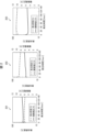
- FIG. 1 is a cross-sectional view showing a schematic configuration of a light-emitting element according to the present disclosure. Three graphs are shown showing the relationship between the emission illuminance and the driving voltage with respect to the emission time in the comparative light-emitting element. 13 is a graph showing the relationship between light emission luminance and light emission time in a comparative light emitting element.
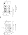
- FIG. 1 is a diagram illustrating a cause of a decrease in the luminance of a comparative light-emitting layer.
- FIG. 2 is a band gap diagram of a hole transport layer, a comparative light-emitting layer, and an electron transport layer in a comparative light-emitting element.
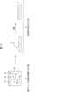
- FIG. 1 is a diagram illustrating a cause of a decrease in the luminance of a comparative light-emitting layer.
- FIG. 2 is a band gap diagram of a hole transport layer, a comparative light-emitting layer, and an electron transport layer in a comparative light-emitting element.
- FIG. 1 illustrates a method for synthesizing a metal sulfide precursor according to the present disclosure.
- FIG. 1 shows the results of photoelectron yield (PYS) measurement of a metal sulfide monolayer. This figure shows the voltage-current characteristics of a hole-only device (HOD) showing hole injection into the quantum dot layer contained in each sulfide medium.
- FIG. 13 is a graph showing the maximum EQE of a light-emitting element using a quantum dot layer contained in each sulfide medium as a light-emitting layer and the rate of decrease in luminance after five hours of operation.
- 1A to 1C are diagrams illustrating a method for manufacturing a light-emitting device according to the present disclosure.
- 1 is a schematic diagram illustrating a configuration example of a display device according to the present disclosure.
- 1 is a cross-sectional view showing a configuration example of a display device according to the present disclosure.
- FIG. 1 is a cross-sectional view showing a schematic configuration of a light-emitting element 101 according to the present disclosure.
- the light-emitting element 101 includes an anode 1, a hole transport layer 2, a light-emitting layer 3, an electron transport layer 4, and a cathode 5.
- the anode 1, the hole transport layer 2, the light-emitting layer 3, the electron transport layer 4, and the cathode 5 may be stacked in this order from the substrate (not shown) side, or may be stacked in the reverse order.
- the light-emitting element 101 has a light-emitting layer 3 that emits light when a current flows between the anode 1 and the cathode 5.
- the light-emitting element 101 may be a QLED (quantum dot light-emitting diode) element.
- the light-emitting layer 3 is located between the anode 1 and the cathode 5.
- the hole transport layer 2 is located between the anode 1 and the light-emitting layer 3.
- the electron transport layer 4 is located between the cathode 5 and the light-emitting layer 3.
- the light-emitting layer 3 has a continuous film 6 and a plurality of light-emitting quantum dots 7.
- An example of a material for the electron transport layer 4 is ZnMgO.
- the continuous film 6 contains a plurality of quantum dots 7.
- containing means that the continuous film 6 covers a part or the whole of the surface of each quantum dot 7, for example.
- the continuous film 6 may be a single film that is not separated by a material other than the continuous film 6.
- the continuous film 6 may have an area of 1000 nm2 or more when viewed from the top of the light-emitting element 101, and may be an integral film that is connected without interruption by chemical bonds of the material that constitutes the continuous film 6.
- the continuous film 6 is formed, for example, so as to partially or completely fill the space formed between the plurality of quantum dots 7 contained in the continuous film 6. There may be a gap in the light-emitting layer 3.
- the plurality of quantum dots 7 contained in the continuous film 6 may be present at intervals from each other.
- the continuous film 6 is mainly composed of a sulfide of Zn (zinc) and a sulfide of an additive metal consisting of at least one of Cd (cadmium), Sn (tin), Mn (manganese), Ga (gallium), In (indium), Ce (cerium), and Cu (copper).
- the molar fraction of the additive metal constituting the sulfide of the additive metal relative to the Zn constituting the sulfide of Zn is 1 mol % or more.
- the continuous film 6 is mainly composed of primary sulfides, which are Zn sulfides, and secondary sulfides.
- the secondary sulfides consist of at least one of Cd sulfides, Sn sulfides, Mn sulfides, Ga sulfides, In sulfides, Ce sulfides, and Cu sulfides.
- the molar fraction of Zn belonging to the primary sulfides is taken as 100 mol %
- the total molar fraction of Cd, Sn, Mn, Ga, In, Ce, and Cu belonging to the secondary sulfides is 1 mol % or more.
- the continuous film 6 is mainly composed of a metal sulfide.
- the difference between the first level of the electron transport layer 4 and the first level of the continuous film 6 is ⁇ E(e), and the difference between the second level of the hole transport layer 2 and the second level of the continuous film 6 is ⁇ E(h).
- the difference between ⁇ E(e) and ⁇ E(h) is 1 eV or less.
- the metal sulfide contains at least one of Zn sulfide, Cd sulfide, Sn sulfide, Mn sulfide, Ga sulfide, In sulfide, Ce sulfide, and Cu sulfide.
- the first level is the CBM or LUMO.
- the second level is the VBM or HOMO.
- the CBM is the bottom of the conduction band.
- the VBM is the top of the valence band.
- the LUMO is the energy level of the lowest unoccupied molecular orbital.
- the HOMO is the energy level of the highest occupied molecular orbital.
- LUMO and HOMO are negative values (unit: eV) with the vacuum level as the reference (0).
- CBM and VBM are mainly for inorganic materials, and LUMO and HOMO are mainly for organic materials. It is possible to replace either the CBM or LUMO with the other. It is possible to replace either the VBM or HOMO with the other.
- Consisting primarily of a certain material encompasses the following cases: (1) made of material A, and (2) containing a small amount of impurities in addition to (1) but capable of achieving the same functionality as (1).
- the quantum dots 7 are luminescent and may include at least one of crystals of II-VI group semiconductors such as MgS, MgSe, MgTe, CaS, CaSe, CaTe, SrS, SrSe, SrTe, BaS, BaSe, BaTe, ZnS, ZnSe, ZnTe, CdS, CdSe, CdTe, HgS, HgSe, and HgTe, crystals of III-V group semiconductors such as GaAs, GaP, InN, InAs, InP, and InSb, crystals of IV group semiconductors such as Si and Ge, and crystals of a perovskite structure such as CsPbI3 , CsPbBr3 , and CsPbCl3 .
- II-VI group semiconductors such as MgS, MgSe, MgTe, CaS, CaSe, CaTe, SrS, SrSe, SrTe
- the band gap of the continuous film 6 may be larger than the band gap of the multiple light-emitting quantum dots 7.
- multiple quantum dots 7 By incorporating multiple quantum dots 7 into a continuous film whose main component is Zn sulfide (the molar fraction of the added metal relative to Zn is less than 1 mol%) to form a light-emitting device, energy transfer between the multiple quantum dots 7 is unlikely to occur, making it possible to achieve high reliability, but the light-emitting efficiency may be low.
- a continuous film containing Zn sulfide as a main component (the molar fraction of the added metal relative to Zn is less than 1 mol%) is used instead of the continuous film 6.
- This continuous film is also called a comparative continuous film.
- a light-emitting layer having a comparative continuous film is also called a comparative light-emitting layer.
- a light-emitting element having a comparative light-emitting layer is also called a comparative light-emitting element.
- Figure 2 shows three graphs that indicate the relationship between the emission time (unit: hour) and the emission illuminance (unit: %) and the driving voltage (unit: V) for the comparative light-emitting element.
- the three graphs 201 to 203 shown in Figure 2 respectively show the cases where the molar concentration of ZnS (Zn sulfide) in the comparative continuous film is as follows.
- the luminous efficiency (EQE) per current is roughly proportional to the emission illuminance.
- Graph 201 0.08M (equivalent to mol/l)
- Graph 202 0.04M
- Graph 203 0.02M 2
- the maximum emission illuminance does not vary significantly depending on the molar concentration of ZnS in the comparative continuous film.
- the maximum value of EQE corresponding to the maximum emission illuminance is approximately 7.0%.
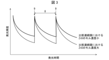
- Figure 3 is a graph showing the relationship between emission luminance (arbitrary units) and emission time (arbitrary units) for a comparative light-emitting element.
- period 8 is the period during which the comparative light-emitting element emits light continuously
- timing 9 is the timing at which the continuous emission of the comparative light-emitting element stops and resumes.
- the emission luminance of the comparative light-emitting element peaks at timing 9, then decreases as the emission time passes within period 8, and peaks again at the next timing 9. Comparing the cases where the molar concentration of ZnS in the comparative continuous film is large and small, it can be seen that the rate of decrease in the emission luminance of the comparative light-emitting element is greater when the molar concentration of ZnS in the comparative continuous film is large.
- Figure 4 is a diagram explaining the factors that cause the emission luminance of the comparative light-emitting layer 10 to decrease.
- the electrons 11 and holes 12 recombine in the center of the comparative light-emitting layer 10, enabling highly efficient light emission.
- the carrier balance in the comparative light-emitting element is poor (excess electrons), electrons 11 gradually accumulate in the comparative light-emitting layer 10, and the electrons 11 accumulated in the comparative light-emitting layer 10 pass through a trion state and are thermally deactivated, making it difficult to achieve highly efficient light emission.
- FIG. 5 is a band gap diagram of the hole transport layer 2, the comparative light-emitting layer 10, and the electron transport layer 4 in the comparative light-emitting element. Comparing the cases where the molar concentration of ZnS in the comparative continuous film 13 is large and small, the injection of holes 12 into the quantum dots 7 tends to be suppressed in the comparative continuous film 13 when the molar concentration of ZnS in the comparative continuous film 13 is large.
- FIG. 6 is a diagram showing a method for synthesizing a metal sulfide precursor according to the present disclosure.
- the metal sulfide may be a sulfide that is the main component of the continuous film 6.
- FIG. 6 illustrates the reaction of zinc xanthate.
- a quantum dot layer corresponding to the light-emitting layer 3 was prepared as follows. Materials are not limited to these as long as they have the same function.
- the octane solution containing the InP/ZnS quantum dots modified with oleic acid was mixed with the DMF solution containing zinc chloride and zinc xanthate, and the two layers were separated and stirred vigorously to transfer the quantum dots to the DMF layer.
- the quantum dots modified with xanthic acid and chloride ions were precipitated by adding ethyl acetate, and the precipitate was dispersed again in a DMF solution containing a xanthogen metal of a predetermined concentration.
- FIG. 7 shows the results of photoelectron yield (PYS) measurements of metal sulfide monolayers.
- PYS measurements were performed to measure the valence band state (VBM) of the metal sulfide of the media.
- VBM valence band state
- a DMF solution of only the xanthate metal precursor of each media was applied onto ITO and then heated at 150°C to form a metal sulfide monolayer corresponding to continuous film 6.
- the VBM increased, and it was confirmed that when used in a media containing quantum dots, the energy barrier required to inject holes from the HOMO of the hole transport layer corresponding to hole transport layer 2 to the quantum dots becomes smaller, making it easier to inject holes.
- the energy levels vary depending on the measurement method, measurement conditions, and fitting method, but when measured using the same method, the relative level relationship can be considered correct.
- Figure 8 shows the voltage-current characteristics of a hole-only device (HOD) that shows the hole injection property into the quantum dot layer contained in each sulfide medium.
- HODs were fabricated to compare the hole injection property of quantum dot layers in which quantum dots are dispersed in each sulfide medium. In the HOD, only holes are injected as carriers.
- the HOD was fabricated to have a layered structure of ITO/NiO nanoparticles/poly-TPD/quantum dots/PMA/Ag.
- the ligands of the quantum dots were replaced with zinc xanthate, and a DMF solution with a quantum dot concentration of 15 mg/ml was prepared, and the molar concentration of the sulfide precursor mixed into the quantum dot solution was adjusted to a specified ratio.
- a phosphomolybdic acid (PMA) solution was applied to the quantum dot layer and baked at 110°C.
- FIG. 9 shows the maximum EQE of the light-emitting element corresponding to the light-emitting element 101, in which the quantum dot layer contained in each sulfide medium is used as the light-emitting layer, and the luminance decrease rate after 5 hours of operation.
- the light-emitting element having the quantum dot layer in which the quantum dots are dispersed in each sulfide medium was fabricated to have a laminated structure of ITO/NiO nanoparticles/poly-TPD/quantum dots/ZnMgO/Ag.
- the ligand of the quantum dots having a composition of InP/ZnS and emitting red light was replaced with zinc xanthate and zinc chloride, and a DMF solution with a quantum dot concentration of 15 mg/ml was prepared, and the molar concentration of the sulfide precursor mixed in the quantum dot solution was adjusted to a predetermined ratio.
- the EQE was increased by replacing 20% of the Zn in the ZnS medium with Cd. Furthermore, it was confirmed that the decrease in luminance at the beginning of operation was suppressed. This is thought to be the effect of improved hole injection properties making it difficult for excess electrons to accumulate in the quantum dot layer.
- Cd is used as an additive to ZnS, but an appropriate amount of a metal that forms a sulfide semiconductor with a higher VBM than ZnS may also be added.
- FIG. 10 shows a first example 14, a second example 15, a third example 16, and a fourth example 17 with respect to the ratio of the mass of the multiple light-emitting quantum dots 7 to the mass of the light-emitting layer 3.
- the light-emitting layer 3 has a single layer structure of the normal arrangement layer 18.
- the light-emitting layer 3 has a laminate structure of two normal arrangement layers 18.
- the light-emitting layer 3 has a laminate structure of the normal arrangement layer 18 (hole transport layer 2 side) and the sparse arrangement layer 19 (electron transport layer 4 side).
- the light-emitting layer 3 has a laminate structure of the sparse arrangement layer 19 (hole transport layer 2 side) and the normal arrangement layer 18 (electron transport layer 4 side).
- the ratio of the mass of the plurality of luminescent quantum dots 7 contained in the normally arranged layer 18 to the mass of the normally arranged layer 18 is 88%.
- the ratio of the mass of the plurality of luminescent quantum dots 7 contained in the sparsely arranged layer 19 to the mass of the sparsely arranged layer 19 is 65%.
- Each of the third example 16 and the fourth example 17 was able to achieve a higher EQE in the light-emitting element 101 compared to the first example 14.
- the second example 15 did not show any improvement in the EQE in the light-emitting element 101 compared to the first example 14.
- the light-emitting layer 3 has a laminated structure of multiple layers including a sparsely arranged layer 19, and the mass ratio of the multiple light-emitting quantum dots 7 contained in the sparsely arranged layer 19 to the mass of the sparsely arranged layer 19 may be 20% or more and 80% or less. As a specific example, it may be any of the configurations of Example 3 16 and Example 4 17 (wherein the ratio is 65%).
- FIG. 11 is a diagram showing a method for manufacturing the light-emitting element 101.
- the method for manufacturing the light-emitting element 101 includes a step S1 of dispersing a first metal complex 20, a second metal complex 21, and a number of light-emitting quantum dots 7 in a solvent 22 to prepare a quantum dot dispersion liquid 23, and a step S2 of applying and heating the quantum dot dispersion liquid 23 to form a light-emitting layer 3.
- the first metal complex 20 is thermally decomposable and contains Zn.
- Examples of the first metal complex 20 include zinc dithiocarboxylate, zinc xanthogenate, zinc dithiocarbamate, and zinc tertiary alkylthiolate.
- Tertiary alkylthiol has a structure represented by R 2 C-SH.
- the second metal complex 21 is thermally decomposable and contains an additive metal.
- the additive metal is at least one of Cd, Sn, Mn, Ga, In, Ce, and Cu.
- Examples of ligands of the second metal complex 21 include dithiocarboxylic acid, xanthic acid, dithiocarbamic acid, and tertiary alkylthiol.
- the solvent 22 may be a polar solvent or a non-polar solvent.
- the solvent 22 may be a polar solvent including at least one of a formamide-based solvent, an acetamide-based solvent, an ester-based solvent, a ketone-based solvent, a sulfoxide solvent, an ether-based solvent, a thioether-based solvent, and a nitrile-based solvent.
- the manufacturing method of the light-emitting element 101 may include a step of exposing and developing the applied quantum dot dispersion liquid 23.
- the display device 401 includes a display unit DA including a plurality of subpixels SP, a first driver X1 and a second driver X2 that drive the plurality of subpixels SP, and a display controller DC that controls the first driver X1 and the second driver X2.
- the subpixel SP includes a light-emitting element 305 and a pixel circuit PC that is connected to the light-emitting element 305.
- the pixel circuit PC may be connected to a scanning signal line GL, a data signal line DL, and a light-emitting control line EL.
- the scanning signal line GL and the light-emitting control line EL may be connected to the first driver X1, and the data signal line DL may be connected to the second driver X2.
- the display device 401 may include a pixel circuit substrate 313 including a substrate 311 and a pixel circuit layer 312, a light emitting element layer 314, and a sealing layer 315.
- the substrate 311 may be a glass substrate, a resin substrate, or the like.
- the substrate 311 may be flexible.
- the pixel circuit layer 312 includes a plurality of pixel circuits PC arranged, for example, in an inorganic matrix.
- the pixel circuit PC may include a pixel capacitance to which a grayscale signal is written, a transistor that controls the current value of the light emitting element 305 according to the grayscale signal, a transistor connected to a scanning signal line GL and a data signal line DL, and a transistor connected to a light emitting control line EL.
- the display device 401 includes a pixel circuit board 313 and a light emitting element layer 314.
- the light emitting element layer 314 may include, in order from the pixel circuit board 313 side, a first electrode D1, an edge cover film JF covering the edge of the first electrode D1, a first functional layer FK, a light emitting layer (quantum dot layer) 330, a second functional layer SK, and a second electrode D2.
- the first functional layer FK may have a hole injection function and a hole transport function
- the second functional layer SK may have an electron transport function.
- the light emitting element layer 314 may include a light emitting element 305R including a light emitting layer 330R that emits red light, a light emitting element 305G including a light emitting layer 330G that emits green light, and a light emitting element 305B including a light emitting layer 330B that emits blue light.
- the sealing layer 315 includes an inorganic insulating film such as a silicon nitride film or a silicon oxide film, and prevents foreign matter (water, oxygen, etc.) from entering the light emitting element layer 314.
- organic materials such as poly[(9,9-dioctylfluorenyl-2,7-diyl)-co-(4,4'-(N-4-sec-butylphenyl))diphenylamine)] (TFB), poly(4-butyltriphenylamine) (p-TPD), poly(9-vinylcarbazole) (PVK), [9,9'-[1,2-phenylenebis(methylene)]bis[N3,N3,N6,N6-tetrakis(4-methoxyphenyl)-9H-carbazole-3,6-diamine] (V886), 7,7'-bi[1,4]benzoxazino[2,3,4-kl]phenoxazine (HN-D1), and inorganic materials such as NiO nanoparticles can be used.
- organic materials such as (2,2',2''-(1,3,5-benzinetriyl)-tris(1-phenyl-1-H-benzimidazole) (TPBi), bathocuproine (BCP), nanoparticles of organometallic complexes, and inorganic materials such as nanoparticles of n-type oxide semiconductors can be used.
- organometallic complexes for example, tris(8-quinolinol)aluminum complex (Alq3) can be used.
- metal oxides such as ZnO and ZnMgO can be used.
- the quantum dot layer is used as the light-emitting layer 330, but this is not limiting.
- the quantum dot layer can also be used as a wavelength conversion layer or a photosensor layer.
- a power generating element can be configured with a quantum dot layer between a pair of electrodes. For example, an electromotive force can be generated by generating holes and electrons in the quantum dots from light incident on the quantum dot layer and transporting each to an electrode.
- the light-emitting element 101 can be used as the light-emitting element 305.
- the anode 1 can be used as the first electrode D1
- the hole transport layer 2 can be used as the first functional layer FK
- the light-emitting layer 3 can be used as the light-emitting layer 330
- the electron transport layer 4 can be used as the second functional layer SK
- the cathode 5 can be used as the second electrode D2.
Landscapes
- Engineering & Computer Science (AREA)
- Manufacturing & Machinery (AREA)
- Physics & Mathematics (AREA)
- Optics & Photonics (AREA)
- Chemical & Material Sciences (AREA)
- Crystallography & Structural Chemistry (AREA)
- Inorganic Chemistry (AREA)
- Nanotechnology (AREA)
- Materials Engineering (AREA)
- Luminescent Compositions (AREA)
- Electroluminescent Light Sources (AREA)
Abstract
Description
グラフ202:0.04M
グラフ203:0.02M
図2によれば、比較発光素子においては、比較連続膜におけるZnSのモル濃度の大小によって、発光照度の最大値に大幅な違いはない。当該発光照度の最大値に対応するEQEの最大値は、およそ7.0%である。
(b)比較発光素子の継続的な発光に対する、比較発光素子の発光輝度の低下量が大きい
本開示による効果を確認するための実験を行った。以下、図6~図9を参照して、当該実験から得られた知見について説明する。
金属硫化物前駆体として各種キサントゲン酸金属錯体を合成して用いた。塩化亜鉛または塩化カドミウムを純水に溶解し、2.5倍モル量のエチルキサントゲン酸カリウムと混合して、12時間攪拌した後、キサントゲン酸金属の沈殿を回収して純水で3回洗浄した。キサントゲン酸金属は150℃でほとんどが分解されて金属硫化物となる。
オレイン酸により修飾されたInP/ZnS量子ドットを含むオクタン溶液と、塩化亜鉛およびキサントゲン酸亜鉛を含むDMF溶液と、を混合し、2層に分離したまま激しく攪拌して、量子ドットをDMF層に移した。キサントゲン酸および塩化物イオンにより修飾された量子ドットを、酢酸エチルを添加して沈殿し、沈殿を所定の濃度のキサントゲン金属を含むDMF溶液に再度分散した。
キサントゲン酸で修飾された量子ドットと各キサントゲン酸金属を含むDMF溶液とを基板に塗布し、150℃で30分加熱することにより、キサントゲン酸金属を熱分解し、連続膜6に対応する金属硫化物の連続膜に量子ドットが包含された量子ドット層を形成した。
2 正孔輸送層
3 発光層
4 電子輸送層
5 カソード
6 連続膜
7 量子ドット
8 期間
9 タイミング
10 比較発光層
11 電子
12 正孔
13 比較連続膜
14 第1例
15 第2例
16 第3例
17 第4例
18 通常配置層
19 疎配置層
20 第1金属錯体
21 第2金属錯体
22 溶媒
23 量子ドット分散液
101、305 発光素子
201、202、203 グラフ
401 表示装置
Claims (7)
- アノードと、
カソードと、
前記アノードと前記カソードとの間に位置している発光層と、を備えており、
前記発光層は、
Znの硫化物と、Cd、Sn、Mn、Ga、In、Ce、およびCuの少なくとも1つからなる添加金属の硫化物と、を主成分としている連続膜であって、前記Znに対する前記添加金属のモル分率が1モル%以上である連続膜と、
前記連続膜に内包された複数の発光性の量子ドットと、を有している、発光素子。 - アノードと、
カソードと、
前記アノードと前記カソードとの間に位置している発光層と、
前記アノードと前記発光層との間に位置している正孔輸送層と、
前記カソードと前記発光層との間に位置している電子輸送層と、を備えており、
前記発光層は、
金属の硫化物を主成分としている連続膜であって、CBMまたはLUMOを第1準位とし、VBMまたはHOMOを第2準位とし、前記電子輸送層の第1準位と前記連続膜の第1準位との差をΔE(e)とし、前記正孔輸送層の第2準位と前記連続膜の第2準位との差をΔE(h)としたとき、ΔE(e)とΔE(h)との差が1eV以下である連続膜と、
前記連続膜に内包された複数の発光性の量子ドットと、を有している、発光素子。 - 前記発光層は、疎配置層を含む複数の層の積層構造であり、
前記疎配置層の質量に対する前記複数の発光性の量子ドットのうち前記疎配置層に含まれているものの質量の比率は、20%以上かつ80%以下である、請求項1または2に記載の発光素子。 - 前記連続膜のバンドギャップは、前記複数の発光性の量子ドットのバンドギャップより大きい、請求項1から3のいずれか1項に記載の発光素子。
- 請求項1から4のいずれか1項に記載の発光素子を備えている、表示装置。
- Znを含む熱分解性の第1金属錯体、Cd、Sn、Mn、Ga、In、Ce、およびCuの少なくとも1つからなる添加金属を含む熱分解性の第2金属錯体、ならびに多数の発光性の量子ドットを溶媒に分散させて量子ドット分散液を調製する工程と、
前記量子ドット分散液を塗布および加熱させて、発光層を形成する工程と、を含んでいる、発光素子の製造方法。 - 塗布した前記量子ドット分散液を露光および現像させる工程を含んでいる、請求項6に記載の発光素子の製造方法。
Priority Applications (3)
| Application Number | Priority Date | Filing Date | Title |
|---|---|---|---|
| PCT/JP2023/011691 WO2024201549A1 (ja) | 2023-03-24 | 2023-03-24 | 発光素子、表示装置、および発光素子の製造方法 |
| JP2025509051A JPWO2024201549A1 (ja) | 2023-03-24 | 2023-03-24 | |
| CN202380096305.4A CN120836192A (zh) | 2023-03-24 | 2023-03-24 | 发光元件、显示装置以及发光元件的制造方法 |
Applications Claiming Priority (1)
| Application Number | Priority Date | Filing Date | Title |
|---|---|---|---|
| PCT/JP2023/011691 WO2024201549A1 (ja) | 2023-03-24 | 2023-03-24 | 発光素子、表示装置、および発光素子の製造方法 |
Publications (1)
| Publication Number | Publication Date |
|---|---|
| WO2024201549A1 true WO2024201549A1 (ja) | 2024-10-03 |
Family
ID=92903986
Family Applications (1)
| Application Number | Title | Priority Date | Filing Date |
|---|---|---|---|
| PCT/JP2023/011691 Ceased WO2024201549A1 (ja) | 2023-03-24 | 2023-03-24 | 発光素子、表示装置、および発光素子の製造方法 |
Country Status (3)
| Country | Link |
|---|---|
| JP (1) | JPWO2024201549A1 (ja) |
| CN (1) | CN120836192A (ja) |
| WO (1) | WO2024201549A1 (ja) |
Citations (4)
| Publication number | Priority date | Publication date | Assignee | Title |
|---|---|---|---|---|
| JP2002338961A (ja) * | 2001-02-07 | 2002-11-27 | Agfa Gevaert Nv | 銅でドーピングされたZnS粒子の製造 |
| WO2005071764A1 (ja) * | 2004-01-23 | 2005-08-04 | Hoya Corporation | 量子ドット分散発光素子およびその製造方法 |
| CN109119543A (zh) * | 2018-08-31 | 2019-01-01 | 嘉兴纳鼎光电科技有限公司 | 异质结结构量子点及其合成方法与应用 |
| US20210074939A1 (en) * | 2019-09-10 | 2021-03-11 | Samsung Display Co., Ltd. | Quantum dot composition, light emitting element and display device including the same |
-
2023
- 2023-03-24 JP JP2025509051A patent/JPWO2024201549A1/ja active Pending
- 2023-03-24 WO PCT/JP2023/011691 patent/WO2024201549A1/ja not_active Ceased
- 2023-03-24 CN CN202380096305.4A patent/CN120836192A/zh active Pending
Patent Citations (4)
| Publication number | Priority date | Publication date | Assignee | Title |
|---|---|---|---|---|
| JP2002338961A (ja) * | 2001-02-07 | 2002-11-27 | Agfa Gevaert Nv | 銅でドーピングされたZnS粒子の製造 |
| WO2005071764A1 (ja) * | 2004-01-23 | 2005-08-04 | Hoya Corporation | 量子ドット分散発光素子およびその製造方法 |
| CN109119543A (zh) * | 2018-08-31 | 2019-01-01 | 嘉兴纳鼎光电科技有限公司 | 异质结结构量子点及其合成方法与应用 |
| US20210074939A1 (en) * | 2019-09-10 | 2021-03-11 | Samsung Display Co., Ltd. | Quantum dot composition, light emitting element and display device including the same |
Also Published As
| Publication number | Publication date |
|---|---|
| JPWO2024201549A1 (ja) | 2024-10-03 |
| CN120836192A (zh) | 2025-10-24 |
Similar Documents
| Publication | Publication Date | Title |
|---|---|---|
| KR101658691B1 (ko) | 안정적이고 모든 용액에 처리 가능한 양자점 발광 다이오드 | |
| US9419174B2 (en) | Transparent quantum dot light-emitting diodes with dielectric/metal/dielectric electrode | |
| JP2019160796A (ja) | 電界発光素子及び表示装置 | |
| US20100245218A1 (en) | Light-emitting device and display device | |
| EP3905355B1 (en) | Quantum dot light-emitting diode and preparation method therefor | |
| US11101441B2 (en) | Quantum dot light-emitting diode and manufacturing method thereof | |
| US12593560B2 (en) | Light-emitting element and display device | |
| CN112331790A (zh) | 发光器件及其制备方法和显示装置 | |
| US20250204146A1 (en) | Light-emitting element | |
| JP7733837B2 (ja) | 発光素子および表示装置 | |
| JP7818094B2 (ja) | 発光素子、表示装置、発光素子の製造方法 | |
| WO2024201549A1 (ja) | 発光素子、表示装置、および発光素子の製造方法 | |
| US20250133902A1 (en) | Light emitting element | |
| KR102784423B1 (ko) | 전자 수송층 및 이를 포함하는 양자점 발광 소자 | |
| US20250294959A1 (en) | Light-emitting element and display device | |
| WO2024018509A1 (ja) | 発光素子、表示装置、および発光素子の製造方法 | |
| CN117356180B (zh) | 发光器件及其制作方法、显示基板和显示装置 | |
| Yan et al. | CdSe‐based Quantum Dot Light‐emitting Diodes | |
| US20260068428A1 (en) | Light-emitting element, and display device | |
| WO2024218888A1 (ja) | 発光素子、表示装置、および発光素子の製造方法 | |
| WO2025203203A1 (ja) | 発光素子、表示装置、発光素子の製造方法 | |
| CN120077737A (zh) | 发光元件、显示装置以及发光层的形成方法 | |
| WO2025203170A1 (ja) | 発光素子、表示装置、および発光素子の製造方法 | |
| WO2024121919A1 (ja) | 量子ドット溶液、発光素子、表示装置及び発光層の形成方法 | |
| CN115884615A (zh) | 量子点发光器件和显示面板 |
Legal Events
| Date | Code | Title | Description |
|---|---|---|---|
| 121 | Ep: the epo has been informed by wipo that ep was designated in this application |
Ref document number: 23930191 Country of ref document: EP Kind code of ref document: A1 |
|
| ENP | Entry into the national phase |
Ref document number: 2025509051 Country of ref document: JP Kind code of ref document: A |
|
| WWE | Wipo information: entry into national phase |
Ref document number: 2025509051 Country of ref document: JP |
|
| WWE | Wipo information: entry into national phase |
Ref document number: 202380096305.4 Country of ref document: CN |
|
| WWP | Wipo information: published in national office |
Ref document number: 202380096305.4 Country of ref document: CN |
|
| NENP | Non-entry into the national phase |
Ref country code: DE |
|
| 122 | Ep: pct application non-entry in european phase |
Ref document number: 23930191 Country of ref document: EP Kind code of ref document: A1 |