WO2024195638A1 - インダクタ部材の製造方法及びインダクタ部材 - Google Patents
インダクタ部材の製造方法及びインダクタ部材 Download PDFInfo
- Publication number
- WO2024195638A1 WO2024195638A1 PCT/JP2024/009632 JP2024009632W WO2024195638A1 WO 2024195638 A1 WO2024195638 A1 WO 2024195638A1 JP 2024009632 W JP2024009632 W JP 2024009632W WO 2024195638 A1 WO2024195638 A1 WO 2024195638A1
- Authority
- WO
- WIPO (PCT)
- Prior art keywords
- protrusion
- hole
- wirings
- inductor
- magnetic
- Prior art date
- Legal status (The legal status is an assumption and is not a legal conclusion. Google has not performed a legal analysis and makes no representation as to the accuracy of the status listed.)
- Ceased
Links
Images









Classifications
-
- H—ELECTRICITY
- H01—ELECTRIC ELEMENTS
- H01F—MAGNETS; INDUCTANCES; TRANSFORMERS; SELECTION OF MATERIALS FOR THEIR MAGNETIC PROPERTIES
- H01F17/00—Fixed inductances of the signal type
- H01F17/04—Fixed inductances of the signal type with magnetic core
-
- H—ELECTRICITY
- H01—ELECTRIC ELEMENTS
- H01F—MAGNETS; INDUCTANCES; TRANSFORMERS; SELECTION OF MATERIALS FOR THEIR MAGNETIC PROPERTIES
- H01F27/00—Details of transformers or inductances, in general
- H01F27/28—Coils; Windings; Conductive connections
- H01F27/29—Terminals; Tapping arrangements for signal inductances
-
- H—ELECTRICITY
- H01—ELECTRIC ELEMENTS
- H01F—MAGNETS; INDUCTANCES; TRANSFORMERS; SELECTION OF MATERIALS FOR THEIR MAGNETIC PROPERTIES
- H01F41/00—Apparatus or processes specially adapted for manufacturing or assembling magnets, inductances or transformers; Apparatus or processes specially adapted for manufacturing materials characterised by their magnetic properties
- H01F41/02—Apparatus or processes specially adapted for manufacturing or assembling magnets, inductances or transformers; Apparatus or processes specially adapted for manufacturing materials characterised by their magnetic properties for manufacturing cores, coils, or magnets
- H01F41/04—Apparatus or processes specially adapted for manufacturing or assembling magnets, inductances or transformers; Apparatus or processes specially adapted for manufacturing materials characterised by their magnetic properties for manufacturing cores, coils, or magnets for manufacturing coils
-
- H—ELECTRICITY
- H01—ELECTRIC ELEMENTS
- H01F—MAGNETS; INDUCTANCES; TRANSFORMERS; SELECTION OF MATERIALS FOR THEIR MAGNETIC PROPERTIES
- H01F5/00—Coils
- H01F5/04—Arrangements of electric connections to coils, e.g. leads
Definitions
- the present invention relates to a method for manufacturing an inductor component and an inductor component.
- Inductor components are used as circuit elements mounted in various electronic devices.
- a sheet-shaped inductor component that includes wiring and a magnetic layer in which the wiring is embedded has also been disclosed (see, for example, Patent Document 1).
- the inductor member disclosed in Patent Document 1 has a number of adjacent wirings spaced apart from each other. Each of the wirings has a hole, such as a via, that penetrates from one surface of the magnetic layer in the thickness direction toward the wiring and houses a conductive member.
- the present invention aims to provide a method for manufacturing inductor components with high processing accuracy.
- a method for manufacturing an inductor member includes a first step of fabricating a magnetic structure having a conductor and an insulating film covering the circumferential surface of the conductor, at least two wirings arranged at different positions in a first direction, and a magnetic layer in which the at least two wirings are embedded; a second step of forming at least two first holes, each connected to a different one of the at least two wirings, using a router or drilling method; a third step of forming an insulating first protrusion inside the first hole; a fourth step of forming a second hole penetrating the first protrusion; and a fifth step of forming a conductive second protrusion in the second hole, connected to the conductor of the wiring.
- the present invention makes it possible to improve the processing accuracy of inductor components.
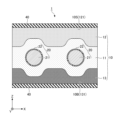
- FIG. 1 is a plan view of an inductor member manufactured by a method for manufacturing an inductor member according to a first embodiment.
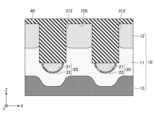
- 2 is a cross-sectional view taken along line AA of FIG. 1. This is a cross-sectional view taken along line B-B of FIG. 3 is a plan view illustrating a first step of the method for manufacturing an inductor component according to the first embodiment.
- FIG. 4 is a cross-sectional view illustrating a first step of a method for manufacturing an inductor component according to the first embodiment.
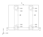
- FIG. 4 is a plan view illustrating a second step of the method for manufacturing the inductor component according to the first embodiment.
- FIG. 4 is a cross-sectional view illustrating a second step of the method for manufacturing the inductor component according to the first embodiment.
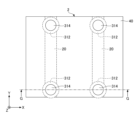
- FIG. 4 is a plan view illustrating a third step of the method for manufacturing an inductor component according to the first embodiment.
- FIG. 4 is a cross-sectional view illustrating a third step of the method for manufacturing an inductor component according to the first embodiment.
- FIG. 11 is a plan view illustrating a fourth step of the method for manufacturing an inductor component according to the first embodiment.
- FIG. 10 is a cross-sectional view illustrating a fourth step of the method for manufacturing an inductor component according to the first embodiment.
- FIG. 10A to 10C are cross-sectional views illustrating another form of the second hole formed in the fourth step of the method for manufacturing the inductor component according to the first embodiment.
- FIG. 11 is a plan view illustrating a fifth step of the method for manufacturing an inductor component according to the first embodiment.
- FIG. 10 is a cross-sectional view illustrating a fifth step of the method for manufacturing an inductor component according to the first embodiment.
- FIG. 11A to 11C are cross-sectional views illustrating another form of the second protrusion formed in the fifth step of the method for manufacturing the inductor component according to the first embodiment.
- 11 is a plan view of an inductor member manufactured by a method for manufacturing an inductor member according to a second embodiment.
- FIG. 13 is a plan view illustrating a second step of the method for manufacturing an inductor component according to the second embodiment.
- FIG. 11 is a cross-sectional view illustrating a second step of the method for manufacturing an inductor component according to the second embodiment.
- FIG. 11 is a cross-sectional view illustrating a second step of the method for manufacturing an inductor component according to the second embodiment.
- FIG. 13 is a plan view illustrating a fourth step of the method for manufacturing an inductor component according to the second embodiment.
- FIG. A cross-sectional view illustrating a fourth step of the method for manufacturing an inductor component according to the second embodiment. 13 is a plan view illustrating another form of the second hole formed in the fourth step of the manufacturing method of the inductor component according to the second embodiment.
- FIG. 1 is a plan view of the inductor member 1.
- Figure 2 is a cross-sectional view taken along the line A-A in Figure 1.
- Figure 3 is a cross-sectional view taken along the line B-B in Figure 1.
- the X direction shown in the figure corresponds to the width direction of the inductor member 1.
- the Y direction corresponds to the depth direction of the inductor member 1.
- the Z direction corresponds to the thickness direction of the inductor member 1.
- the X and Y directions are sometimes referred to as the "in-plane directions" of the inductor member 1.
- the Z direction is sometimes referred to as the "perpendicular to the plane direction" of the inductor member 1.
- the X, Y, and Z directions are mutually perpendicular.
- the magnetic laminate 10 has a rectangular planar shape. Also, as shown in Figs. 2 and 3, the magnetic laminate 10 has a front surface 10S located on one side in the Z direction and a back surface 10B located on the other side in the Z direction. Each of the front surface 10S and back surface 10B of the magnetic laminate 10 of the first embodiment is covered with an insulating film 40.
- the front surface 10S of the magnetic laminate 10 is an example of a "first surface" of the magnetic layer.
- the back surface 10B of the magnetic laminate 10 is an example of a "second surface" of the magnetic layer.
- the magnetic laminate 10 preferably has multiple magnetic layers from the viewpoint of increasing the inductance value and the DC superposition characteristics. More specifically, the magnetic laminate 10 has a first magnetic layer 11, a second magnetic layer 12 arranged on one side of the first magnetic layer 11 in the Z direction, and a third magnetic layer 13 arranged on the other side of the first magnetic layer 11 in the Z direction. The first magnetic layer 11 is arranged between the second magnetic layer 12 and the third magnetic layer 13.
- the second magnetic layer 12 corresponds to the top layer of the magnetic laminate 10. Therefore, the surface 10S of the magnetic laminate 10 corresponds to the surface 121 located on one side of the second magnetic layer 12 in the Z direction. Also, the third magnetic layer 13 corresponds to the bottom layer of the magnetic laminate 10. Therefore, the back surface 10B of the magnetic laminate 10 corresponds to the back surface 131 located on the other side of the third magnetic layer 13 in the Z direction.
- the magnetic laminate 10 is not limited to being composed of multiple magnetic layers. That is, the magnetic laminate 10 may be, for example, a single-layer structure consisting of only the first magnetic layer 11.
- the first magnetic layer 11 has a predetermined thickness in the Z direction and is in the form of a sheet extending in an in-plane direction. As shown in FIG.
- the first magnetic layer 11 includes magnetic particles and a binder that holds the magnetic particles.
- the shape of the magnetic particles is not particularly limited, but examples include an approximately spherical shape, an approximately needle shape, and an approximately flat shape.
- the material of the magnetic particles in the first magnetic layer 11 is not particularly limited, but examples include soft magnetic materials and hard magnetic materials. Among these, soft magnetic materials are preferred from the viewpoint of increasing the inductance value and DC superposition characteristics of the inductor member 1.
- Soft magnetic bodies include, for example, single metal bodies that contain one type of metal element in a pure substance state, and alloy bodies that are eutectic bodies (mixtures) of one or more types of metal elements (first metal elements) and one or more types of metal elements (second metal elements) and/or non-metal elements (carbon, nitrogen, silicon, phosphorus, etc.). These can be used alone or in combination.
- An example of a single metal body is a metal element consisting of only one type of metal element (first metal element).
- the first metal element is appropriately selected from among metal elements that can be contained as the first metal element in a soft magnetic body, such as iron (Fe), cobalt (Co), nickel (Ni), and others.
- examples of the single metal body include a form including a core containing only one type of metal element and a surface layer containing an inorganic and/or organic substance that modifies a part or all of the surface of the core, and a form in which an organometallic compound or an inorganic metal compound containing a first metal element is decomposed (e.g., thermally decomposed).
- examples of the form in which an organometallic compound or an inorganic metal compound containing a first metal element is decomposed include iron powder (sometimes called carbonyl iron powder) obtained by thermally decomposing an organoiron compound (specifically, iron pentacarbonyl) containing iron as the first metal element.
- the position of the layer containing an inorganic and/or organic substance that modifies the part containing only one type of metal element is not limited to the surface as described above.
- the organometallic compound or inorganic metal compound from which a single metal body can be obtained is not particularly limited, and can be appropriately selected from known or commonly used organometallic compounds or inorganic metal compounds from which a single metal body of a soft magnetic material can be obtained.
- the alloy body is a eutectic of one or more metal elements (first metal elements) and one or more metal elements (second metal elements) and/or non-metal elements (carbon, nitrogen, silicon, phosphorus, etc.), and is not particularly limited as long as it can be used as an alloy body of a soft magnetic material.
- the first metal element is an essential element in the alloy body, and examples of such elements include iron (Fe), cobalt (Co), and nickel (Ni). If the first metal element is Fe, the alloy body is an Fe-based alloy; if the first metal element is Co, the alloy body is a Co-based alloy; and if the first metal element is Ni, the alloy body is a Ni-based alloy.
- the second metal element is an element (secondary component) secondarily contained in the alloy body, and is a metal element that is compatible (eutectic) with the first metal element, and examples of such elements include iron (Fe) (when the first metal element is other than Fe), cobalt (Co) (when the first metal element is other than Co), nickel (Ni) (when the first metal element is other than Ni), chromium (Cr), aluminum (Al), silicon (Si), copper (Cu), silver (Ag), manganese (Mn), calcium (Ca), and burr.
- Nonmetallic elements are elements (secondary components) secondarily contained in the alloy body, and are nonmetallic elements that are compatible (eutectic) with the first metallic element, such as boron (B), carbon (C), nitrogen (N), silicon (Si), phosphorus (P), and sulfur (S). These can be used alone or in combination of two or more types.
- alloy bodies such as Fe-based alloys
- alloy bodies include magnetic stainless steel (Fe-Cr-Al-Si alloy) (including electromagnetic stainless steel), Sendust (Fe-Si-Al alloy) (including super Sendust), Permalloy (Fe-Ni alloy), Fe-Ni-Mo alloy, Fe-Ni-Mo-Cu alloy, Fe-Ni-Co alloy, Fe-Cr alloy, Fe-Cr-Al alloy, Fe-Ni-Cr alloy, Fe-Ni-Cr-Si alloy, silicon copper (Fe-Cu-Si alloy), Fe-Si alloy, Fe-Si-B (-Cu-Nb) alloy, Fe-B-Si-Cr alloy, Fe- Examples include Si-Cr-Ni alloys, Fe-Si-Cr alloys, Fe-Si-Al-Ni-Cr alloys, Fe-Ni-Si-Co alloys, Fe-N alloys, Fe-C alloys, Fe-B alloys, Fe-P alloys
- alloy bodies such as Co-based alloys
- Co-based alloys include Co-Ta-Zr and cobalt (Co)-based amorphous alloys.
- alloy bodies, such as Ni-based alloys include Ni-Cr alloys.
- binders include thermoplastic components such as acrylic resins, and thermosetting components such as epoxy resin compositions.
- Acrylic resins include, for example, carboxyl-containing acrylic acid ester copolymers.
- Epoxy resin compositions include, for example, an epoxy resin (such as cresol novolac epoxy resin) as a base, a curing agent for epoxy resins (such as phenolic resins), and a curing accelerator for epoxy resins (such as imidazole compounds).
- thermoplastic component and a thermosetting component can be used alone or in combination, and preferably a thermoplastic component and a thermosetting component are used in combination.
- the thickness of the first magnetic layer 11 is not particularly limited, but is, for example, 100 ⁇ m or more, preferably 200 ⁇ m or more, and is, for example, 2000 ⁇ m or less, preferably 1500 ⁇ m or less, and more preferably 1000 ⁇ m or less.
- the thickness of the first magnetic layer 11 is the distance between the top of the surface of the first magnetic layer 11 on one side in the Z direction (upper side in FIG. 2) and the bottom of the surface on the other side in the Z direction (lower side in FIG. 2).
- the regions directly above and below each wiring 20 in the first magnetic layer 11 are preferably raised in accordance with the outer peripheral shape of the wiring 20. More specifically, the regions directly above the wiring 20 in the first magnetic layer 11 are preferably located higher than the regions between the wirings 20. Also, the regions directly below the wiring 20 in the first magnetic layer 11 are preferably located lower than the regions between the wirings 20.
- the first magnetic layer 11 can be formed to follow the magnetic field generated around each wiring 20, compared to when the first magnetic layer 11 is flat. This makes it possible to increase the inductance value more effectively.
- the shape of the first magnetic layer 11 is not limited to this.
- the second magnetic layer 12 has a predetermined thickness and is in the form of a sheet extending in the in-plane direction.
- An insulating film 40 is disposed on a surface 121 of the second magnetic layer 12.
- the second magnetic layer 12 also includes magnetic particles and a binder.
- the third magnetic layer 13 has a predetermined thickness and is in the form of a sheet extending in the in-plane direction. Like the first magnetic layer 11 and the second magnetic layer 12, the third magnetic layer 13 also has magnetic particles and a binder. Examples of the magnetic particles of the second magnetic layer 12 and the magnetic particles of the third magnetic layer 13 are similar to the magnetic particles exemplified for the first magnetic layer 11. Examples of the binder of the second magnetic layer 12 and the binder of the third magnetic layer 13 are similar to the binder exemplified for the first magnetic layer 11.
- the second magnetic layer 12 preferably has a higher relative magnetic permeability than the first magnetic layer 11 by appropriately changing the type, shape, etc. of the magnetic particles. This makes it possible to increase the inductance value of the inductor member 1.
- the third magnetic layer 13 preferably has a higher relative magnetic permeability than the first magnetic layer 11 by appropriately changing the type, shape, etc. of the magnetic particles. This makes it possible to increase the inductance value of the inductor member 1.
- the magnetic particles in the first magnetic layer 11 have an isotropic shape, such as a substantially spherical shape
- the multiple wirings 20 are arranged inside the magnetic laminate 10 as shown in Figures 1 to 3. As shown in Figure 1, the multiple wirings 20 are arranged at different positions in the X direction at intervals. In the embodiment of Figure 1, "different positions" includes the case where the wirings are arranged at a distance in the X direction. However, the direction in which the multiple wirings 20 are arranged is not limited to the X direction. The direction in which the multiple wirings 20 are arranged may be referred to as the "first direction" hereinafter. In the case of the first embodiment, the X direction corresponds to the first direction.
- the multiple wirings 20 each extend along the Y direction.
- Each of the multiple wirings 20 has, for example, an inductance value according to the length of the wiring 20.
- the spacing between adjacent wirings 20 may be equal or different.
- Each wiring 20 is electrically connected to a terminal pair 30.
- the wiring 20 is electrically connected to both the first terminal portion 31 and the second terminal portion 32 that constitute the terminal pair 30.
- the wiring 20 corresponds to a path of current that is input from one of the first terminal portion 31 or the second terminal portion 32 in the terminal pair 30 and output from the other.
- the wiring 20 has a conductor 21 and an insulating film 22 that covers the circumferential surface of the conductor 21.
- the cross-sectional shape of the conductor 21 is circular, but may be other shapes such as an ellipse or a polygon.
- the material of the conductor 21 may be, for example, a metal conductor such as copper, silver, gold, aluminum, nickel, or an alloy of these. Copper is preferable.
- the conductor 21 may have a single-layer structure, or a multi-layer structure in which the surface of a core conductor (e.g., copper) is plated (e.g., nickel).
- the conductor 21 in the first embodiment is copper, but is not limited to this.
- the radius of the conductor 21 is, for example, 25 ⁇ m or more, preferably 50 ⁇ m or more, and, for example, 2000 ⁇ m or less, preferably 200 ⁇ m or less.
- the insulating film 22 protects the conductor 21 from chemicals and water, and prevents a short circuit between the conductor 21 and the magnetic laminate 10 (first magnetic layer 11).
- the insulating film 22 covers the entire outer surface (circumferential surface) of the conductor 21.
- the insulating film 22 has a generally circular ring shape in cross section that is concentric with the wiring 20.
- Examples of materials for the insulating film 22 include insulating resins such as polyvinyl formal, polyester, polyesterimide, polyamide (including nylon), polyimide, polyamideimide, and polyurethane. These may be used alone or in combination of two or more types. Furthermore, the insulating film 22 may be composed of a single layer or multiple layers.
- the thickness of the insulating film 22 is approximately uniform in the radial direction of the wiring 20 at any position in the circumferential direction, and is, for example, 1 ⁇ m or more, preferably 3 ⁇ m or more, and, for example, 100 ⁇ m or less, preferably 50 ⁇ m or less.
- the ratio of the radius of the conductor 21 to the thickness of the insulating film 22 is, for example, 1 or more, preferably 5 or more, and, for example, 500 or less, preferably 100 or less.
- the inductor member 1 has a plurality of terminal pairs 30. As shown in Fig. 1, each of the plurality of terminal pairs 30 is electrically connected to a different one of the plurality of wirings 20. Although the illustrated terminal pairs 30 are connected one by one to each of the wirings 20, a plurality of terminal pairs 30 may be connected to each of the wirings 20.
- Each of the multiple terminal pairs 30 has a first terminal portion 31 and a second terminal portion 32.
- the first terminal portion 31 of the terminal pair 30 may function as an input terminal for the current supplied to the wiring 20.
- the second terminal portion 32 of the terminal pair 30 may function as an output terminal for the current supplied to the wiring 20.
- the first terminal portion 31 of the terminal pair 30 may function as an output terminal for the current supplied to the wiring 20.
- the second terminal portion 32 of the terminal pair 30 may function as an input terminal for the current supplied to the wiring 20.
- the first terminal portion 31 of the terminal pair 30 located on one side in the X direction (left side in FIG. 1) and the first terminal portion 31 of the terminal pair 30 located on the other side in the X direction (right side in FIG. 1) are disposed at different positions in the X direction and are adjacent to each other.
- the second terminal portion 32 of the terminal pair 30 located on one side in the X direction and the second terminal portion 32 of the terminal pair 30 located on the other side in the X direction are disposed at different positions in the X direction and are adjacent to each other.
- the arrangement of the first terminal portion 31 and the second terminal portion 32 in the multiple terminal pairs 30 is not limited to this.
- first terminal portion 31 (second terminal portion 32) of the terminal pair 30 located on one side in the X direction and the second terminal portion 32 (first terminal portion 31) of the terminal pair 30 located on the other side in the X direction may be adjacent to each other in the X direction.
- the first terminal portion 31 and the second terminal portion 32 of the terminal pair 30 are provided from the surface 10S on one side of the magnetic laminate 10 in the Z direction, or the back surface 10B on the other side of the Z direction, toward the wiring 20 within the magnetic laminate 10. However, this is not limited to this.
- each of the first terminal portion 31 and the second terminal portion 32 has an insulating first protrusion portion 312 and a conductive second protrusion portion 314. Since the second terminal portion 32 has a similar configuration to the first terminal portion 31, a description of the second terminal portion 32 will be omitted below.
- the outermost portion of the first protrusion 312 contacts the first magnetic layer 11 of the magnetic laminate 10.
- the first protrusion 312 is disposed at the outermost portion of the first terminal portion 31.
- the first protrusion 312 in the first embodiment is a cylindrical (columnar) insulating portion that protrudes from the surface 10S of the magnetic laminate 10 toward the wiring 20. As shown in FIG. 1, the planar shape of the first protrusion 312 is substantially circular. However, the shape of the first protrusion 312 is not limited to this.
- the first protrusion 312 may be connected, for example, to the insulating film 40 that covers the surface 10S of the magnetic laminate 10.
- the first protrusion 312 may be made of the same insulating material as the insulating film 40.
- the material of the first protrusion 312 and the insulating film 40 is not particularly limited, but one example is a resin such as epoxy. However, without being limited thereto, the first protrusion 312 may be made of an insulating material different from the insulating film 40.
- the first protrusion 312 is physically connected to the conductor 21 of the wiring 20.
- the bottom surface 312B of the first protrusion 312 reaches the inside of the conductor 21.
- the bottom surface 312B of the first protrusion 312 may be flat, or may have a tapered portion in which the width of the first protrusion 312 narrows as it progresses toward the bottom.
- the maximum width W1 of the first protrusion 312 is greater than the maximum width of the wiring 20, i.e., the diameter W2.
- the second protrusion 314 is a portion for supplying the current input from the circuit to which the inductor member 1 is connected to the wiring 20, or for outputting the current flowing through the wiring 20 to the circuit. More specifically, the second protrusion 314 is disposed inside the first protrusion 312 and is a conductive rod-shaped portion that penetrates the first protrusion 312.
- the material of the second protrusion 314 is not particularly limited, but examples include metal conductors such as copper, silver, gold, aluminum, nickel, tin, indium, bismuth, and alloys thereof.
- the second protrusion 314 preferably extends along the Z direction.
- the method for manufacturing an inductor member according to the first embodiment includes the steps of fabricating a magnetic structure, forming a first hole in the magnetic structure, forming an insulating first protrusion inside the first hole, forming a second hole penetrating the insulating first protrusion, and forming a conductive second protrusion in the second hole. Each step is described in detail below.
- Figure 4A is a plan view of the magnetic structure 2.
- Figure 4B is a cross-sectional view taken along the cutting line C-C in Figure 4A.
- the magnetic structure 2 includes a magnetic laminate 10 (magnetic layer) and wiring 20.
- the process for producing the magnetic structure 2 may be referred to as the "first process.”
- multiple wirings 20 are embedded inside the magnetic laminate 10. More specifically, from the other side in the Z direction to one side in the Z direction, the third magnetic layer 13, the first magnetic layer 11 including multiple wirings 20 aligned in the X direction, and the second magnetic layer 12 are stacked in this order, and then the stacked magnetic layers are pressed using a pressure means such as an isostatic press. Note that the method for producing the magnetic structure 2 is not limited to this.
- Figure 5A is a plan view of the magnetic structure 2 in which the first hole portion 311 is formed.
- Figure 5B is a cross-sectional view taken along the cutting line D-D in Figure 5A.
- the step of forming the first hole portion 311 may be referred to as the "second step.”
- the second step is performed following the first step.
- a first hole 311 is formed that is recessed from the surface of the magnetic structure 2, i.e., the surface 10S of the magnetic laminate 10, toward the wiring 20.
- the bottom surface 311B of the first hole 311 reaches the conductor 21 of the wiring 20 embedded in the magnetic laminate 10.
- the bottom surface 311B of the first hole 311 intersects with the center (core) of the conductor 21 or reaches a position deeper than the center (core) of the conductor 21.
- the width 311W of the first hole 311 is greater than the maximum width of the wiring 20, i.e., the diameter W2. This allows the entire width of the wiring 20 to be exposed.
- first holes 311 are formed for each wiring 20.
- two first holes 311 are formed for each of the two wirings 20. Therefore, the number of first holes 311 shown in FIG. 5A is four. However, the number of first holes 311 is not limited to this.
- the two first holes 311 formed for each wiring 20 one is formed for the first terminal portion 31, and the other is formed for the second terminal portion 32. Furthermore, of the first holes 311 formed in different wirings 20, the two first holes 311 located on the upper side of FIG. 5A are adjacent to each other in the X direction. Similarly, of the first holes 311 formed in different wirings 20, the two first holes 311 located on the lower side of FIG. 5A are also adjacent to each other in the X direction. However, the positional relationship of each of the first holes 311 is not limited to this.
- All four first holes 311 are formed from the surface 10S side of the magnetic laminate 10, but are not limited to this.
- the method for forming the first hole portion 311 is preferably a method using a cutting tool such as a router end mill or a drill.
- a method using a router end mill may be referred to as the "router processing method.”
- a method using a drill may be referred to as the "drill processing method.”
- a "router end mill” is a cutting tool that is attached to a machine tool such as a router machine that performs cutting processing of printed wiring boards, film materials, etc.
- a router end mill has a long rod-shaped cutting part along the rotation axis, and is equipped with a blade formed on the side of the cutting part.
- the router processing method and drill processing method use a cutting tool with a rod-shaped (approximately cylindrical) cutting portion, such as a router end mill or a drill.
- a cutting tool with a rod-shaped (approximately cylindrical) cutting portion, such as a router end mill or a drill.
- the router end mill or drill is lowered in the Z direction from the surface 10S of the magnetic laminate 10 to form a first hole portion 311 in the magnetic laminate 10 that extends approximately perpendicular to the surface 10S.
- the first hole 311 has a columnar shape with the side surface 311S of the first hole 311 aligned along the Z direction. Therefore, the first hole 311 has a substantially constant width regardless of the position in the Z direction (depth direction). That is, in a cross-sectional view, the opposing side surfaces of the first hole 311 can be made parallel to each other.
- the router processing method or drill processing method it is possible to form a deep hole with a high aspect ratio (hole depth/maximum width of the hole) in a compact manner, compared to hole processing methods in which the width on one side in the Z direction is larger than the width on the other side in the Z direction, such as the blast processing method in which holes are formed by colliding abrasive particles or the laser processing method in which holes are formed by irradiating laser light.
- the first hole 311 is formed from the back surface 10B of the magnetic laminate 10 using a router end mill or drill.
- the bottom surface 311B of the first hole 311 has a flat shape.
- the bottom surface 311B of the first hole 311 has a tapered portion in which the width of the first hole 311 narrows as it progresses toward the bottom.
- Figure 6A is a plan view of the magnetic structure 2 on which the first protrusions 312 are formed.
- Figure 6B is a cross-sectional view taken along the line E-E in Figure 6A.
- the process of forming the first protrusions 312 may be referred to as the "third process.”
- the third step is performed following the second step.
- an insulating film is filled inside each of the first holes 311 to form the first protrusions 312.
- an insulating film including the area of the first protrusion 312 is laminated onto the surface 10S of the magnetic laminate 10.
- the laminated insulating film may also include an area of the insulating film 40 that is continuous with the first protrusion 312.
- the method of forming the first protrusion 312 is not limited to this. The first hole 311 is blocked by forming the insulating first protrusion 312.
- the opposing side surfaces of the first protrusion 312 can be made parallel to each other. Since the first hole 311 is a deep hole with a high aspect ratio, the first protrusion 312 can also be formed as a compact protrusion with a high aspect ratio.
- Figure 7A is a plan view of the magnetic structure 2 in which the second hole portion 313 is formed.
- Figure 7B is a cross-sectional view taken along the line F-F in Figure 7A.
- the step of forming the second hole portion 313 may be referred to as the "fourth step.”
- the fourth step is performed following the third step.
- the second hole portion 313 is formed from the surface 3121 located on one side in the Z direction of each first protrusion 312 toward the other side in the Z direction.
- Examples of methods for forming the second hole 313 include a router process, a drill process, a blast process, and a laser process. Among these, it is preferable to use the router process and the drill process.
- a rod-shaped (approximately cylindrical) cutting tool such as a router end mill or a drill can be lowered along the Z direction from the surface 10S of the magnetic laminate 10, for example, to form a deep hole with a high aspect ratio in the first protrusion 312.
- the opposing side surfaces of the second hole portion 313 can be made parallel to each other in a cross-sectional view.
- the side surface 313S of the second hole portion 313 can be formed approximately parallel to the side surface 312S of the first protrusion 312. This prevents the second hole portion 313 from breaking through the side surface 312S of the first protrusion 312 and being formed outside the first protrusion 312.
- a tapered portion 313T having a shape similar to the tip of a drill can be formed on the bottom surface 313B of the second hole 313.
- a conductive second protrusion 314 is formed in the second hole 313, and a tapered portion 314T is formed on the bottom surface 314B of the second protrusion 314 following the tapered portion 313T of the second hole 313 (see FIG. 9B).
- This increases the contact area between the second protrusion 314 and the conductor 21 of the wiring 20, reducing the resistance at the interface between them.
- the bottom surface 313B is, for example, flat (see FIG. 8).
- the drilling method or the router method it is possible to form a compact deep hole with a high aspect ratio (hole depth/maximum hole width) compared to hole processing methods in which the width on one side in the Z direction is larger than the width on the other side in the Z direction, such as the blasting method, which forms holes by colliding abrasive particles, or the laser processing method, which forms holes by irradiating laser light.
- the second hole 313 penetrates the first protrusion 312 in the thickness direction. That is, the bottom surface 313B of the second hole 313 reaches the conductor 21 of the wiring 20 and is deeper than the bottom surface 312B of the first protrusion 312. The second hole 313 is physically connected to the conductor 21 of the wiring 20.
- the width 311W of the first hole 311 is larger than the maximum width W2 of the wiring 20 (see FIG. 5B). Accordingly, the width 312W of the first protrusion 312 is larger than the maximum width W2 of the wiring 20. Therefore, by forming the second hole 313 substantially vertically using the position of the first protrusion 312 as a marker, the bottom surface 313B of the second hole 313 can be reliably connected to the conductor 21 of the wiring 20.
- Figure 9A is a plan view of the magnetic structure 2 on which the second protrusions 314 are formed.
- Figure 9B is a cross-sectional view taken along the line G-G in Figure 9A.
- the step of forming the second protrusions 314 may be referred to as the "fifth step.”
- the fifth step is performed following the fourth step.
- a conductor is filled into the second hole 313.
- the method for filling the second protrusion 314 with the conductor is not particularly limited, but examples include electrolytic plating, electroless plating, and a method of applying a sintered or thermosetting conductive paste.
- a sintered conductive paste is preferable from the viewpoint of reducing electrical resistance.
- the bottom surface 314B of the second protrusion 314 reaches the inside of the conductor 21 of the wiring 20. That is, the second protrusion 314 is electrically connected to the wiring 20.
- the bottom surface 314B of the second protrusion 314 is deeper than the bottom surface 312B of the first protrusion 312.
- the bottom surface 314B of the second protrusion 314 has a tapered portion 314T in which the width of the second protrusion 314 narrows as it advances toward the bottom. This increases the contact area between the second protrusion 314 and the conductor 21 of the wiring 20. As a result, the resistance generated at the interface between the second protrusion 314 and the conductor 21 can be reduced.
- the opposing side surfaces of the second protrusion 314 can be made parallel to each other in a cross-sectional view. Since the second hole 313 is a deep hole with a high aspect ratio, the second protrusion 314 also becomes a protrusion with a high aspect ratio.
- the side walls of the second hole 313 are parallel to each other, so the degree of shrinkage due to thermal shrinkage is uniform, and the occurrence of cracks in the conductor that constitutes the second protrusion 314 can be suppressed.
- the bottom surface 314B of the second protrusion 314 is formed flat, as shown in Figures 8 and 10.
- the first terminal portion 31 and the second terminal portion 32 are produced by forming the second protrusion portion 314 in the second hole portion 313. Furthermore, the inductor member 1 can be manufactured through the first to fifth steps.
- the first hole 311 After forming the first hole 311 by the router processing method or the drill processing method, the first hole 311 is filled with an insulating film, so that, for example, the first protrusion 312 that extends substantially perpendicularly from the surface 10S of the magnetic laminate 10 and has a high aspect ratio can be formed.
- the second hole 313 that penetrates in the Z direction (thickness direction) is formed inside the first protrusion 312, and the second hole 313 is filled with a conductive film, so that the second protrusion 314 that is conductive and has a high aspect ratio like the first protrusion 312 can be formed.
- the second protrusion 314 can be appropriately connected to each of these wirings 20.
- the processing accuracy can be improved so that each of the multiple wirings 20 and each terminal portion (first terminal portion 31, second terminal portion 32) can be electrically and physically connected.
- the second protrusions 314 can be insulated from each other even if the distance between the second protrusions 314 connected to each of the multiple wirings 20 becomes close. As a result, it is possible to prevent situations such as a short circuit occurring between adjacent second protrusions 314, and to suppress a decrease in the yield of the inductor member 1.
- the second hole 313 penetrating the inside of the first protrusion 312 and the second protrusion 314 are formed. Therefore, the bottom surface 314B of the second protrusion 314 can be reliably connected to the conductor 21 of the wiring 20. This allows for proper electrical continuity between the conductor 21 and the second protrusion 314.
- Fig. 11 is a plan view of the inductor member 1A.
- the inductor member 1A has a magnetic laminate 10, a plurality of wirings 20, a terminal pair 30A having a first terminal portion 31A and a second terminal portion 32A, and an insulating film 40.
- the structures of the first terminal portion 31A and the second terminal portion 32A are different from the first terminal portion 31 and the second terminal portion 32 of the inductor member 1 manufactured by the manufacturing method of the inductor member according to the first embodiment. Note that the structure of the second terminal portion 32A is similar to the structure of the first terminal portion 31A, and therefore a description of the second terminal portion 32A is omitted.
- the first terminal portion 31A has an insulating first protrusion 312A and a conductive second protrusion 314A. As shown in FIG. 11, the first protrusion 312A has a planar shape that is elongated in the Y direction. In other words, the longitudinal direction of the first protrusion 312A is aligned with the longitudinal direction of the wiring 20.
- a number of second protrusions 314A are formed inside the first protrusion 312A. All of the second protrusions 314A are connected to the conductors 21 of the wiring 20. Note that the number of second protrusions 314A shown in FIG. 11 is five, but is not limited to this.
- the method for manufacturing an inductor member according to the second embodiment includes a step of producing a magnetic structure (first step), a step of forming a first hole in the magnetic structure (second step), a step of forming an insulating first protrusion inside the first hole (third step), a step of forming a second hole penetrating the insulating first protrusion (fourth step), and a step of forming a conductive second protrusion in the second hole (fifth step).
- Steps 1, 3, and 5 are the same as those in the first embodiment. In contrast, steps 2 and 4 are different from those in the first embodiment.
- Figure 12A is a plan view of the magnetic structure 2 in which the first hole portion 311A is formed.
- Figure 12B is a cross-sectional view taken along the H-H cutting line in Figure 12A.
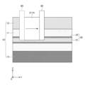
- Figure 13 is a cross-sectional view taken along the I-I cutting line in Figure 12A, and is a diagram for explaining a method of forming the first hole portion 311A.
- a first hole 311A having a predetermined depth in the Z direction is formed in the surface 10S of the magnetic laminate 10 using a router processing method.
- the width W3 of the first hole 311A is larger than the diameter W2 of the wiring 20.
- the first hole 311A extends in the Y direction as shown in Figure 12A.
- the router end mill 60 is lowered from the surface 10S of the magnetic laminate 10 to the other side in the Z direction (the bottom side of the figure). This forms a hole extending in the Z direction in the magnetic laminate 10, which corresponds to one end of the first hole portion 311A. Furthermore, while still inserted in this hole, the router end mill 60 is moved to one side in the Y direction (the right side of the figure). This forms the first hole portion 311A extending in the Y direction in the magnetic laminate 10.
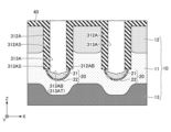
- Figure 14A is a plan view of the magnetic structure 2 in which the second hole portion 313A is formed.
- Figure 14B is a cross-sectional view taken along the cutting line J-J in Figure 14A.
- an insulating film is filled into the first hole 311A. This forms an insulating first protrusion 312A (see FIG. 11) in the first hole 311A. Then, in the fourth step, a plurality of second holes 313A are formed, as shown in FIG. 14A and FIG. 14B.
- each of the multiple second hole portions 313A is not particularly limited, but a drilling method that can form a deep hole with a high aspect ratio along the Z direction inside the first protrusion 312A and form a tapered portion 313AT at the tip is preferable.
- the second hole portion 313A may be formed by a router processing method.
- the planar shape of the second hole portion 313A may be a shape extending in the Y direction as shown in FIG. 15.
- the side surface 313AS of the second hole portion 313A is parallel to the side surface 312AS of the first protrusion portion 312A. It is also preferable that both side surfaces 313AS of the second hole portion 313A are parallel.
- the bottom surface 313AB of the second hole portion 313A is deeper than the bottom surface 312AB of the first protrusion portion 312A.
- each of the second holes 313A is filled with a conductive film.
- the method for manufacturing an inductor component includes the steps of:
- ⁇ 2> The method for manufacturing the inductor component described in ⁇ 1>, in which the second hole portion is formed using a drilling method.
- ⁇ 3> The method for manufacturing an inductor component described in ⁇ 1> or ⁇ 2>, wherein in the fourth step, the second hole is formed so that the bottom surface of the second hole is deeper than the bottom surface of the first hole.
- At least two wirings each having a conductor and an insulating film covering a peripheral surface of the conductor, the wirings being arranged at different positions in a first direction; a magnetic layer in which the at least two wirings are embedded and which has a first surface on one side in a thickness direction and a second surface on the other side in the thickness direction; At least two terminal portions each connected to a different one of the at least two wirings; having The terminal portion is an insulating first protrusion protruding from one of the first surface and the second surface of the magnetic layer toward the wiring; a conductive second protrusion penetrating the first protrusion and connected to the conductor of the wiring; An inductor member having
- ⁇ 6> An inductor member according to ⁇ 4> or ⁇ 5>, in which a plurality of the second protrusions are formed inside the first protrusion.
- ⁇ 8> An inductor component according to any one of ⁇ 4> to ⁇ 7>, in which the opposing side surfaces of the first protrusion are parallel to each other in a cross-sectional view.
- ⁇ 12> An inductor component according to any one of ⁇ 4> to ⁇ 10>, wherein the bottom surface of the first protrusion has a tapered portion in which the width of the first protrusion narrows as it moves toward the bottom.
- Reference Signs List 1 1A Inductor member 2 Magnetic structure 10 Magnetic laminate 10S Surface 10B of magnetic laminate Back surface 11 of magnetic laminate First magnetic layer 12 Second magnetic layer 13 Third magnetic layer 20 Wiring 21 Conductor wire 22 of wiring Insulating film 30, 30A covering the conductor wire Terminal pair 31, 31A First terminal portion 32, 32A Second terminal portion 311, 311A First hole portion 312, 312A First insulating protrusion portion 313, 313A Second hole portion 314, 314A Second conductive protrusion portion 40 Insulating film
Landscapes
- Engineering & Computer Science (AREA)
- Power Engineering (AREA)
- Manufacturing & Machinery (AREA)
- Microelectronics & Electronic Packaging (AREA)
- Coils Or Transformers For Communication (AREA)
- Manufacturing Cores, Coils, And Magnets (AREA)
Priority Applications (3)
| Application Number | Priority Date | Filing Date | Title |
|---|---|---|---|
| CN202480019575.XA CN120814012A (zh) | 2023-03-22 | 2024-03-12 | 电感部件的制造方法和电感部件 |
| EP24774777.7A EP4685830A1 (en) | 2023-03-22 | 2024-03-12 | Method for manufacturing inductor member and inductor member |
| JP2025508345A JPWO2024195638A1 (https=) | 2023-03-22 | 2024-03-12 |
Applications Claiming Priority (2)
| Application Number | Priority Date | Filing Date | Title |
|---|---|---|---|
| JP2023-045792 | 2023-03-22 | ||
| JP2023045792 | 2023-03-22 |
Publications (1)
| Publication Number | Publication Date |
|---|---|
| WO2024195638A1 true WO2024195638A1 (ja) | 2024-09-26 |
Family
ID=92841395
Family Applications (1)
| Application Number | Title | Priority Date | Filing Date |
|---|---|---|---|
| PCT/JP2024/009632 Ceased WO2024195638A1 (ja) | 2023-03-22 | 2024-03-12 | インダクタ部材の製造方法及びインダクタ部材 |
Country Status (5)
| Country | Link |
|---|---|
| EP (1) | EP4685830A1 (https=) |
| JP (1) | JPWO2024195638A1 (https=) |
| CN (1) | CN120814012A (https=) |
| TW (1) | TW202443608A (https=) |
| WO (1) | WO2024195638A1 (https=) |
Citations (4)
| Publication number | Priority date | Publication date | Assignee | Title |
|---|---|---|---|---|
| JP2021028928A (ja) * | 2019-08-09 | 2021-02-25 | 日東電工株式会社 | インダクタ |
| JP2021044294A (ja) * | 2019-09-06 | 2021-03-18 | 株式会社村田製作所 | インダクタ部品 |
| JP2022023412A (ja) | 2020-07-27 | 2022-02-08 | 日東電工株式会社 | インダクタの製造方法 |
| JP2023045792A (ja) | 2021-09-22 | 2023-04-03 | 大日本印刷株式会社 | 加飾シート及び加飾成形品の製造方法 |
-
2024
- 2024-03-12 JP JP2025508345A patent/JPWO2024195638A1/ja active Pending
- 2024-03-12 CN CN202480019575.XA patent/CN120814012A/zh active Pending
- 2024-03-12 EP EP24774777.7A patent/EP4685830A1/en active Pending
- 2024-03-12 WO PCT/JP2024/009632 patent/WO2024195638A1/ja not_active Ceased
- 2024-03-20 TW TW113110349A patent/TW202443608A/zh unknown
Patent Citations (4)
| Publication number | Priority date | Publication date | Assignee | Title |
|---|---|---|---|---|
| JP2021028928A (ja) * | 2019-08-09 | 2021-02-25 | 日東電工株式会社 | インダクタ |
| JP2021044294A (ja) * | 2019-09-06 | 2021-03-18 | 株式会社村田製作所 | インダクタ部品 |
| JP2022023412A (ja) | 2020-07-27 | 2022-02-08 | 日東電工株式会社 | インダクタの製造方法 |
| JP2023045792A (ja) | 2021-09-22 | 2023-04-03 | 大日本印刷株式会社 | 加飾シート及び加飾成形品の製造方法 |
Non-Patent Citations (1)
| Title |
|---|
| See also references of EP4685830A1 |
Also Published As
| Publication number | Publication date |
|---|---|
| CN120814012A (zh) | 2025-10-17 |
| TW202443608A (zh) | 2024-11-01 |
| JPWO2024195638A1 (https=) | 2024-09-26 |
| EP4685830A1 (en) | 2026-01-28 |
Similar Documents
| Publication | Publication Date | Title |
|---|---|---|
| CN110047639B (zh) | 线圈部件 | |
| KR102786140B1 (ko) | 인덕터 | |
| KR20160136127A (ko) | 코일 전자부품 및 그 제조방법 | |
| KR102763843B1 (ko) | 인덕터 | |
| KR20070033253A (ko) | 칩 인덕터 | |
| US20220165483A1 (en) | Inductor | |
| KR20160117989A (ko) | 코일 전자부품 및 그 제조방법 | |
| WO2024195638A1 (ja) | インダクタ部材の製造方法及びインダクタ部材 | |
| CN113474856B (zh) | 电感器 | |
| KR102726093B1 (ko) | 인덕터 | |
| KR102870719B1 (ko) | 인덕터 | |
| WO2024195639A1 (ja) | インダクタ部材 | |
| KR102726084B1 (ko) | 인덕터 | |
| WO2025197832A1 (ja) | インダクタ部材及びインダクタ部材の製造方法 | |
| KR102906502B1 (ko) | 코일 부품 | |
| CN114223043B (zh) | 电感器 | |
| TWI826648B (zh) | 電感器 | |
| TWI877137B (zh) | 電感器及其製造方法 | |
| WO2025192160A1 (ja) | インダクタ | |
| KR20150001385A (ko) | 복합재 및 이를 이용하여 제조된 인덕터 |
Legal Events
| Date | Code | Title | Description |
|---|---|---|---|
| 121 | Ep: the epo has been informed by wipo that ep was designated in this application |
Ref document number: 24774777 Country of ref document: EP Kind code of ref document: A1 |
|
| ENP | Entry into the national phase |
Ref document number: 2025508345 Country of ref document: JP Kind code of ref document: A |
|
| WWE | Wipo information: entry into national phase |
Ref document number: 2025508345 Country of ref document: JP |
|
| WWE | Wipo information: entry into national phase |
Ref document number: 202480019575.X Country of ref document: CN |
|
| WWP | Wipo information: published in national office |
Ref document number: 202480019575.X Country of ref document: CN |
|
| WWE | Wipo information: entry into national phase |
Ref document number: 2024774777 Country of ref document: EP |
|
| NENP | Non-entry into the national phase |
Ref country code: DE |
|
| ENP | Entry into the national phase |
Ref document number: 2024774777 Country of ref document: EP Effective date: 20251022 |
|
| ENP | Entry into the national phase |
Ref document number: 2024774777 Country of ref document: EP Effective date: 20251022 |
|
| ENP | Entry into the national phase |
Ref document number: 2024774777 Country of ref document: EP Effective date: 20251022 |
|
| ENP | Entry into the national phase |
Ref document number: 2024774777 Country of ref document: EP Effective date: 20251022 |
|
| ENP | Entry into the national phase |
Ref document number: 2024774777 Country of ref document: EP Effective date: 20251022 |
|
| ENP | Entry into the national phase |
Ref document number: 2024774777 Country of ref document: EP Effective date: 20251022 |
|
| WWP | Wipo information: published in national office |
Ref document number: 2024774777 Country of ref document: EP |