WO2024190309A1 - 感光性組成物、硬化物、表示装置、及び硬化物の製造方法 - Google Patents
感光性組成物、硬化物、表示装置、及び硬化物の製造方法 Download PDFInfo
- Publication number
- WO2024190309A1 WO2024190309A1 PCT/JP2024/005920 JP2024005920W WO2024190309A1 WO 2024190309 A1 WO2024190309 A1 WO 2024190309A1 JP 2024005920 W JP2024005920 W JP 2024005920W WO 2024190309 A1 WO2024190309 A1 WO 2024190309A1
- Authority
- WO
- WIPO (PCT)
- Prior art keywords
- photosensitive composition
- mass
- group
- resin
- ppm
- Prior art date
- Legal status (The legal status is an assumption and is not a legal conclusion. Google has not performed a legal analysis and makes no representation as to the accuracy of the status listed.)
- Ceased
Links
Images


Classifications
-
- G—PHYSICS
- G03—PHOTOGRAPHY; CINEMATOGRAPHY; ANALOGOUS TECHNIQUES USING WAVES OTHER THAN OPTICAL WAVES; ELECTROGRAPHY; HOLOGRAPHY
- G03F—PHOTOMECHANICAL PRODUCTION OF TEXTURED OR PATTERNED SURFACES, e.g. FOR PRINTING, FOR PROCESSING OF SEMICONDUCTOR DEVICES; MATERIALS THEREFOR; ORIGINALS THEREFOR; APPARATUS SPECIALLY ADAPTED THEREFOR
- G03F7/00—Photomechanical, e.g. photolithographic, production of textured or patterned surfaces, e.g. printing surfaces; Materials therefor, e.g. comprising photoresists; Apparatus specially adapted therefor
- G03F7/004—Photosensitive materials
- G03F7/022—Quinonediazides
- G03F7/023—Macromolecular quinonediazides; Macromolecular additives, e.g. binders
-
- C—CHEMISTRY; METALLURGY
- C08—ORGANIC MACROMOLECULAR COMPOUNDS; THEIR PREPARATION OR CHEMICAL WORKING-UP; COMPOSITIONS BASED THEREON
- C08L—COMPOSITIONS OF MACROMOLECULAR COMPOUNDS
- C08L101/00—Compositions of unspecified macromolecular compounds
-
- G—PHYSICS
- G03—PHOTOGRAPHY; CINEMATOGRAPHY; ANALOGOUS TECHNIQUES USING WAVES OTHER THAN OPTICAL WAVES; ELECTROGRAPHY; HOLOGRAPHY
- G03F—PHOTOMECHANICAL PRODUCTION OF TEXTURED OR PATTERNED SURFACES, e.g. FOR PRINTING, FOR PROCESSING OF SEMICONDUCTOR DEVICES; MATERIALS THEREFOR; ORIGINALS THEREFOR; APPARATUS SPECIALLY ADAPTED THEREFOR
- G03F7/00—Photomechanical, e.g. photolithographic, production of textured or patterned surfaces, e.g. printing surfaces; Materials therefor, e.g. comprising photoresists; Apparatus specially adapted therefor
- G03F7/004—Photosensitive materials
-
- G—PHYSICS
- G03—PHOTOGRAPHY; CINEMATOGRAPHY; ANALOGOUS TECHNIQUES USING WAVES OTHER THAN OPTICAL WAVES; ELECTROGRAPHY; HOLOGRAPHY
- G03F—PHOTOMECHANICAL PRODUCTION OF TEXTURED OR PATTERNED SURFACES, e.g. FOR PRINTING, FOR PROCESSING OF SEMICONDUCTOR DEVICES; MATERIALS THEREFOR; ORIGINALS THEREFOR; APPARATUS SPECIALLY ADAPTED THEREFOR
- G03F7/00—Photomechanical, e.g. photolithographic, production of textured or patterned surfaces, e.g. printing surfaces; Materials therefor, e.g. comprising photoresists; Apparatus specially adapted therefor
- G03F7/004—Photosensitive materials
- G03F7/022—Quinonediazides
- G03F7/0226—Quinonediazides characterised by the non-macromolecular additives
-
- G—PHYSICS
- G03—PHOTOGRAPHY; CINEMATOGRAPHY; ANALOGOUS TECHNIQUES USING WAVES OTHER THAN OPTICAL WAVES; ELECTROGRAPHY; HOLOGRAPHY
- G03F—PHOTOMECHANICAL PRODUCTION OF TEXTURED OR PATTERNED SURFACES, e.g. FOR PRINTING, FOR PROCESSING OF SEMICONDUCTOR DEVICES; MATERIALS THEREFOR; ORIGINALS THEREFOR; APPARATUS SPECIALLY ADAPTED THEREFOR
- G03F7/00—Photomechanical, e.g. photolithographic, production of textured or patterned surfaces, e.g. printing surfaces; Materials therefor, e.g. comprising photoresists; Apparatus specially adapted therefor
- G03F7/004—Photosensitive materials
- G03F7/022—Quinonediazides
- G03F7/023—Macromolecular quinonediazides; Macromolecular additives, e.g. binders
- G03F7/0233—Macromolecular quinonediazides; Macromolecular additives, e.g. binders characterised by the polymeric binders or the macromolecular additives other than the macromolecular quinonediazides
-
- G—PHYSICS
- G03—PHOTOGRAPHY; CINEMATOGRAPHY; ANALOGOUS TECHNIQUES USING WAVES OTHER THAN OPTICAL WAVES; ELECTROGRAPHY; HOLOGRAPHY
- G03F—PHOTOMECHANICAL PRODUCTION OF TEXTURED OR PATTERNED SURFACES, e.g. FOR PRINTING, FOR PROCESSING OF SEMICONDUCTOR DEVICES; MATERIALS THEREFOR; ORIGINALS THEREFOR; APPARATUS SPECIALLY ADAPTED THEREFOR
- G03F7/00—Photomechanical, e.g. photolithographic, production of textured or patterned surfaces, e.g. printing surfaces; Materials therefor, e.g. comprising photoresists; Apparatus specially adapted therefor
- G03F7/004—Photosensitive materials
- G03F7/075—Silicon-containing compounds
- G03F7/0757—Macromolecular compounds containing Si-O, Si-C or Si-N bonds
-
- G—PHYSICS
- G03—PHOTOGRAPHY; CINEMATOGRAPHY; ANALOGOUS TECHNIQUES USING WAVES OTHER THAN OPTICAL WAVES; ELECTROGRAPHY; HOLOGRAPHY
- G03F—PHOTOMECHANICAL PRODUCTION OF TEXTURED OR PATTERNED SURFACES, e.g. FOR PRINTING, FOR PROCESSING OF SEMICONDUCTOR DEVICES; MATERIALS THEREFOR; ORIGINALS THEREFOR; APPARATUS SPECIALLY ADAPTED THEREFOR
- G03F7/00—Photomechanical, e.g. photolithographic, production of textured or patterned surfaces, e.g. printing surfaces; Materials therefor, e.g. comprising photoresists; Apparatus specially adapted therefor
- G03F7/20—Exposure; Apparatus therefor
-
- G—PHYSICS
- G03—PHOTOGRAPHY; CINEMATOGRAPHY; ANALOGOUS TECHNIQUES USING WAVES OTHER THAN OPTICAL WAVES; ELECTROGRAPHY; HOLOGRAPHY
- G03F—PHOTOMECHANICAL PRODUCTION OF TEXTURED OR PATTERNED SURFACES, e.g. FOR PRINTING, FOR PROCESSING OF SEMICONDUCTOR DEVICES; MATERIALS THEREFOR; ORIGINALS THEREFOR; APPARATUS SPECIALLY ADAPTED THEREFOR
- G03F7/00—Photomechanical, e.g. photolithographic, production of textured or patterned surfaces, e.g. printing surfaces; Materials therefor, e.g. comprising photoresists; Apparatus specially adapted therefor
- G03F7/26—Processing photosensitive materials; Apparatus therefor
- G03F7/40—Treatment after imagewise removal, e.g. baking
-
- G—PHYSICS
- G09—EDUCATION; CRYPTOGRAPHY; DISPLAY; ADVERTISING; SEALS
- G09F—DISPLAYING; ADVERTISING; SIGNS; LABELS OR NAME-PLATES; SEALS
- G09F9/00—Indicating arrangements for variable information in which the information is built-up on a support by selection or combination of individual elements
- G09F9/30—Indicating arrangements for variable information in which the information is built-up on a support by selection or combination of individual elements in which the desired character or characters are formed by combining individual elements
-
- H—ELECTRICITY
- H05—ELECTRIC TECHNIQUES NOT OTHERWISE PROVIDED FOR
- H05B—ELECTRIC HEATING; ELECTRIC LIGHT SOURCES NOT OTHERWISE PROVIDED FOR; CIRCUIT ARRANGEMENTS FOR ELECTRIC LIGHT SOURCES, IN GENERAL
- H05B33/00—Electroluminescent light sources
- H05B33/12—Light sources with substantially two-dimensional [2D] radiating surfaces
-
- H—ELECTRICITY
- H05—ELECTRIC TECHNIQUES NOT OTHERWISE PROVIDED FOR
- H05B—ELECTRIC HEATING; ELECTRIC LIGHT SOURCES NOT OTHERWISE PROVIDED FOR; CIRCUIT ARRANGEMENTS FOR ELECTRIC LIGHT SOURCES, IN GENERAL
- H05B33/00—Electroluminescent light sources
- H05B33/12—Light sources with substantially two-dimensional [2D] radiating surfaces
- H05B33/14—Light sources with substantially two-dimensional [2D] radiating surfaces characterised by the chemical or physical composition or the arrangement of the electroluminescent material, or by the simultaneous addition of the electroluminescent material in or onto the light source
-
- H—ELECTRICITY
- H05—ELECTRIC TECHNIQUES NOT OTHERWISE PROVIDED FOR
- H05B—ELECTRIC HEATING; ELECTRIC LIGHT SOURCES NOT OTHERWISE PROVIDED FOR; CIRCUIT ARRANGEMENTS FOR ELECTRIC LIGHT SOURCES, IN GENERAL
- H05B33/00—Electroluminescent light sources
- H05B33/12—Light sources with substantially two-dimensional [2D] radiating surfaces
- H05B33/22—Light sources with substantially two-dimensional [2D] radiating surfaces characterised by the chemical or physical composition or the arrangement of auxiliary dielectric or reflective layers
-
- H—ELECTRICITY
- H10—SEMICONDUCTOR DEVICES; ELECTRIC SOLID-STATE DEVICES NOT OTHERWISE PROVIDED FOR
- H10H—INORGANIC LIGHT-EMITTING SEMICONDUCTOR DEVICES HAVING POTENTIAL BARRIERS
- H10H20/00—Individual inorganic light-emitting semiconductor devices having potential barriers, e.g. light-emitting diodes [LED]
- H10H20/80—Constructional details
-
- H—ELECTRICITY
- H10—SEMICONDUCTOR DEVICES; ELECTRIC SOLID-STATE DEVICES NOT OTHERWISE PROVIDED FOR
- H10H—INORGANIC LIGHT-EMITTING SEMICONDUCTOR DEVICES HAVING POTENTIAL BARRIERS
- H10H20/00—Individual inorganic light-emitting semiconductor devices having potential barriers, e.g. light-emitting diodes [LED]
- H10H20/80—Constructional details
- H10H20/85—Packages
- H10H20/852—Encapsulations
- H10H20/854—Encapsulations characterised by their material, e.g. epoxy or silicone resins
-
- H—ELECTRICITY
- H10—SEMICONDUCTOR DEVICES; ELECTRIC SOLID-STATE DEVICES NOT OTHERWISE PROVIDED FOR
- H10K—ORGANIC ELECTRIC SOLID-STATE DEVICES
- H10K50/00—Organic light-emitting devices
- H10K50/10—OLEDs or polymer light-emitting diodes [PLED]
- H10K50/11—OLEDs or polymer light-emitting diodes [PLED] characterised by the electroluminescent [EL] layers
- H10K50/115—OLEDs or polymer light-emitting diodes [PLED] characterised by the electroluminescent [EL] layers comprising active inorganic nanostructures, e.g. luminescent quantum dots
-
- H—ELECTRICITY
- H10—SEMICONDUCTOR DEVICES; ELECTRIC SOLID-STATE DEVICES NOT OTHERWISE PROVIDED FOR
- H10K—ORGANIC ELECTRIC SOLID-STATE DEVICES
- H10K50/00—Organic light-emitting devices
- H10K50/80—Constructional details
- H10K50/84—Passivation; Containers; Encapsulations
-
- H—ELECTRICITY
- H10—SEMICONDUCTOR DEVICES; ELECTRIC SOLID-STATE DEVICES NOT OTHERWISE PROVIDED FOR
- H10K—ORGANIC ELECTRIC SOLID-STATE DEVICES
- H10K59/00—Integrated devices, or assemblies of multiple devices, comprising at least one organic light-emitting element covered by group H10K50/00
- H10K59/10—OLED displays
- H10K59/12—Active-matrix OLED [AMOLED] displays
- H10K59/122—Pixel-defining structures or layers, e.g. banks
-
- H—ELECTRICITY
- H10—SEMICONDUCTOR DEVICES; ELECTRIC SOLID-STATE DEVICES NOT OTHERWISE PROVIDED FOR
- H10K—ORGANIC ELECTRIC SOLID-STATE DEVICES
- H10K59/00—Integrated devices, or assemblies of multiple devices, comprising at least one organic light-emitting element covered by group H10K50/00
- H10K59/10—OLED displays
- H10K59/17—Passive-matrix OLED displays
- H10K59/173—Passive-matrix OLED displays comprising banks or shadow masks
-
- H—ELECTRICITY
- H10—SEMICONDUCTOR DEVICES; ELECTRIC SOLID-STATE DEVICES NOT OTHERWISE PROVIDED FOR
- H10K—ORGANIC ELECTRIC SOLID-STATE DEVICES
- H10K85/00—Organic materials used in the body or electrodes of devices covered by this subclass
- H10K85/10—Organic polymers or oligomers
-
- H—ELECTRICITY
- H10—SEMICONDUCTOR DEVICES; ELECTRIC SOLID-STATE DEVICES NOT OTHERWISE PROVIDED FOR
- H10K—ORGANIC ELECTRIC SOLID-STATE DEVICES
- H10K85/00—Organic materials used in the body or electrodes of devices covered by this subclass
- H10K85/40—Organosilicon compounds, e.g. TIPS pentacene
Definitions
- the present invention relates to a photosensitive composition, a cured product, a display device, and a method for producing the cured product.
- OLED organic electroluminescence
- LED micro light-emitting diode
- the pixel division layer of an OLED display is formed by photolithography.
- the materials used are required to have high sensitivity during exposure.
- foreign matter may be generated after storage of a photosensitive composition at room temperature, and the foreign matter may remain in the opening of the pixel division layer. Such foreign matter may lead to the generation of dark spots in the pixel area and a shortened lifespan of the light-emitting element. Therefore, the materials used are also required to have excellent storage stability that does not generate foreign matter, etc.
- micro LED displays are expected to be used in new applications such as signage, AR (Augmented Reality), VR (Virtual Reality), and transparent displays.
- AR Augmented Reality
- VR Virtual Reality
- transparent displays In micro LED displays, light is emitted from the LED light source in all directions, so if light is absorbed by the insulating layer, protective layer, or partitions of the surrounding components, the light extraction efficiency will decrease. For this reason, there is a demand for improving brightness through the configuration of the insulating layer, protective layer, or partitions, as well as the physical properties of the materials used.
- photosensitive compositions include positive-type photosensitive compositions that contain polyimide as a resin (see, for example, Patent Document 1) and positive-type photosensitive compositions that contain polysiloxane as a resin (see Patent Document 2).
- compositions described in Patent Document 1 and Patent Document 2 have problems in combining sensitivity during exposure, suppression of residue after development, storage stability, and luminescence brightness. Therefore, further improvements in the properties of photosensitive compositions are desired.
- the object of the present invention is to provide a photosensitive composition that combines excellent sensitivity during exposure, suppression of residues after development, and excellent storage stability, a cured product obtained by curing the photosensitive composition, a method for producing the cured product, and a display device that includes the cured product and has excellent luminous brightness.
- a photosensitive composition comprising (A) a binder resin and (C) a photosensitizer, the (C) photosensitizer contains (C1) a naphthoquinone diazide compound, Further, it contains methanol and/or ethanol,
- the photosensitive composition satisfies the following condition (7): (7)
- the total content of methanol and ethanol in the photosensitive composition is 0.0010 to 30,000 ppm by mass.
- the composition contains one or more selected from the group consisting of 1-methoxy-2-propanol, 1-ethoxy-2-propanol, methyl acetate, ethyl acetate, allyl methyl ether, allyl ethyl ether, isoallyl methyl ether, and isoallyl ethyl ether;
- the total content of 1-methoxy-2-propanol, 1-ethoxy-2-propanol, methyl acetate, ethyl acetate, allyl methyl ether, allyl ethyl ether, isoallyl methyl ether, and isoallyl ethyl ether in the photosensitive composition is 0.0010 to 30,000 ppm by mass.
- the composition contains one or more selected from the group consisting of 2-methoxy-1-propanol, 2-ethoxy-1-propanol, 2-methoxy-1-propyl acetate, 2-ethoxy-1-propyl acetate, methallyl methyl ether, and methallyl ethyl ether;
- the total content of 2-methoxy-1-propanol, 2-ethoxy-1-propanol, 2-methoxy-1-propyl acetate, 2-ethoxy-1-propyl acetate, methallyl methyl ether, and methallyl ethyl ether in the photosensitive composition is 0.0010 to 1,000 ppm by mass.
- the content of water in the photosensitive composition is 0.010 to 3.0% by mass.
- the electrolyte solution contains one or more ions selected from the group consisting of sulfate ions, sulfite ions, nitrate ions, nitrite ions, phosphate ions, phosphite ions, hypophosphite ions, formate ions, acetate ions, and oxalate ions, and satisfies the following condition (4): and/or
- the total content of phosphoric acid esters, phosphonic acid esters, phosphonic acid esters, phosphorous acid esters, phosphinic acid, and hypophosphite esters in the total solid content of the photosensitive composition is 0.0010 to 30,000 ppm by mass.
- the total content of a tertiary amine compound and a quaternary ammonium ion in the total solid content of the photosensitive composition is 0.0010 to 50,000 ppm by mass.
- R 61 represents a hydrogen atom or a monovalent organic group. * 1 to * 3 each independently represent a bonding point in the resin.
- C3 photoacid generator
- C4 photobase generator
- a display device comprising the cured product according to [14] above.
- a method for producing a cured product comprising: (1) a step of forming a coating film of the photosensitive composition according to any one of the above [1] to [13] on a substrate; (2) a step of irradiating the coating film of the photosensitive composition with actinic rays through a photomask; (3) a step of developing the coating film with a developer to form a pattern of the photosensitive composition; and (4) a step of heating the pattern to obtain a cured pattern of the photosensitive composition.
- a display device having a substrate, a redistribution layer, an interlayer insulating layer for the redistribution layer, and a semiconductor chip, and further having a partition layer and/or a planarization layer, the semiconductor chip is a light emitting element, In a plan view, the area of the redistribution layer is larger than the area of the semiconductor chip; the barrier layer is formed between adjacent semiconductor chips, the planarization layer is formed to cover at least a portion of the semiconductor chip;
- the display device wherein the partition layer and/or the planarizing layer contains methanol and/or ethanol and satisfies the following condition (X1a) and/or (X1b):
- (X1a) The total content of methanol and ethanol in the partition layer is 0.0010 to 30,000 ppm by mass.
- (X1b) The total content of methanol and ethanol in the planarizing layer is 0.0010 to 30,000 ppm by mass.
- the photosensitive composition of the present invention can provide excellent sensitivity during exposure, reduced residue after development, and excellent storage stability. In addition, it is possible to provide a cured product that can be used in a display device with excellent luminance. Furthermore, the display device of the present invention can provide a display device with excellent luminance.
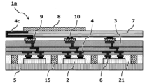
- FIG. 2 is a schematic cross-sectional view of a micro LED display having a barrier layer and a planarization layer.
- FIG. 2 is a schematic cross-sectional view of another form of micro-LED display having a barrier layer and a planarization layer.
- FIG. 1 is a plan view showing a manufacturing process of steps 1 to 4 for a substrate of an organic EL display used in an evaluation of light-emitting characteristics.
- the photosensitive composition of the present invention will be described in detail below along with the embodiments. However, the present invention is not limited to the following embodiments, and various modifications are naturally possible within the scope of the invention, as long as the object of the invention can be achieved and the gist of the invention is not deviated from.
- the main chain of the resin refers to the longest chain among the chains that make up the resin containing structural units.
- the side chain of the resin refers to a chain that is branched from the main chain or bonded to the main chain and has a shorter chain length than the main chain among the chains that make up the resin containing structural units.
- the end of the resin refers to a structure that seals the main chain, such as a structure derived from an end-capping agent.
- the photosensitive composition of the present invention has the above-mentioned configuration [1].
- the photosensitive composition of the present invention can have excellent sensitivity during exposure, suppression of residue after development, and excellent storage stability.
- the photosensitive composition contains a small amount of the above-mentioned methanol and/or ethanol, and the hydrophilicity of the compound promotes dissolution in the developer, which is believed to provide excellent sensitivity during exposure and suppression of residue after development.
- the substrate surface is surface-modified by the compound, it is believed that the effect of suppressing residue after development is achieved by preventing adhesion of residue at the opening.
- the polar groups of the resin in the photosensitive composition are stabilized by the interaction through hydrogen bonds caused by the hydroxyl groups in the compound.
- the photosensitive composition contains polysiloxane, it is suitable for stabilizing the silanol groups in the polysiloxane.
- the hydroxyl groups in the compound control the polarization structure and charge balance in the photosensitive composition. As a result, it is presumed that the effect of excellent storage stability is achieved.
- the above-mentioned compound in the photosensitive composition modifies the surface of the wiring that becomes the opening or the wiring surface that contacts the pattern.
- the hydroxyl groups in the compound contained in the cured product capture trace amounts of metal impurities and ion impurities in the cured product, and these impurities migrate to the wiring surface and act as carriers in the wiring.
- the conductivity of the wiring such as metal is controlled, and low voltage operation is possible, thereby achieving the effect of high luminescence brightness.
- the photosensitive composition of the present invention contains (A) a binder resin.
- the (A) binder resin is a heat-resistant resin that at least a part of which remains in a cured product obtained by curing the composition.
- the (A) binder resin in the composition may remain in a cured product obtained by curing the composition.
- the (A) binder resin is preferably a resin that is cured by forming a crosslinked structure by reaction.
- the reaction is not particularly limited, and may be caused by heating or irradiation with energy rays, and may also be caused by forming a crosslinked structure by a (F) crosslinking agent described later.
- the (A) binder resin is preferably a thermosetting resin.
- the (A) binder resin is preferably an alkali-soluble resin having an acidic group or an organic solvent-soluble resin having an organic solvent-soluble structure.
- the (A) binder resin is preferably a resin that has a solubility capable of forming a positive or negative pattern by imparting positive or negative photosensitivity to the composition by the (C) photosensitizer described below.
- the (A) binder resin preferably has an acidic group in the structural unit of the resin.
- the acidic group is preferably a phenolic hydroxyl group, a hydroxyimide group, a hydroxyamide group, a silanol group, a 1,1-bis(trifluoromethyl)methylol group, a mercapto group, a carboxy group, a carboxylic anhydride group, or a sulfonic acid group, and from the viewpoint of improving sensitivity during exposure and suppressing residues after development, a carboxy group, a carboxylic anhydride group, or a sulfonic acid group is more preferable.
- the binder resin preferably has a radical polymerizable group, and more preferably has a radical polymerizable group in the structural unit of the resin.
- the radical polymerizable group preferably has an ethylenically unsaturated double bond group, and more preferably is a photoreactive group, an alkenyl group having 2 to 5 carbon atoms, or an alkynyl group having 2 to 5 carbon atoms.
- the photoreactive group is preferably a styryl group, a cinnamoyl group, a maleimide group, a nadiimide group, or a (meth)acryloyl group, and from the viewpoint of improving sensitivity during exposure, a (meth)acryloyl group is more preferable.
- the alkenyl group having 2 to 5 carbon atoms or the alkynyl group having 2 to 5 carbon atoms is preferably a vinyl group, an allyl group, a 2-methyl-2-propenyl group, a crotonyl group, a 2-methyl-2-butenyl group, a 3-methyl-2-butenyl group, a 2,3-dimethyl-2-butenyl group, an ethynyl group, or a 2-propargyl group, and from the viewpoint of improving sensitivity during exposure, a vinyl group or an allyl group is more preferable.
- the binder resin (A) preferably contains (A1) a weakly acidic group-containing resin and/or (A2) a resin having no weakly acidic groups.
- the (A) binder resin contains a (A1) weakly acidic group-containing resin
- the (A1) weakly acidic group-containing resin preferably has one or more types of groups selected from the group consisting of a phenolic hydroxyl group, a hydroxyimide group, a hydroxyamide group, a silanol group, a 1,1-bis(trifluoromethyl)methylol group, and a mercapto group as the (WA) weakly acidic group, and more preferably has a (WA) weakly acidic group in the structural unit of the resin.
- these groups may be collectively referred to as the "(WA) weakly acidic group”.
- the (WA) weakly acidic group is preferably a phenolic hydroxyl group, a silanol group, or a 1,1-bis(trifluoromethyl)methylol group (hereinafter, a "specific (WA) weakly acidic group").
- the acidic group possessed by the (A) binder resin is preferably a phenolic hydroxyl group, a hydroxyimide group, a hydroxyamide group, a silanol group, a mercapto group, a carboxy group, a carboxylic anhydride group, or a sulfonic acid group
- the (WA) weak acidic group is preferably one or more groups selected from the group consisting of a phenolic hydroxyl group, a hydroxyimide group, a hydroxyamide group, a silanol group, and a mercapto group.
- the (A1) weak acidic group-containing resin has a remarkable effect of improving sensitivity during exposure, since the solubility of the exposed area is improved due to the moderate acidity of the (WA) weak acidic group and the interaction with the (C) photosensitizer described below.
- a specific (WA) weak acidic group among the (WA) weak acidic groups has a remarkable effect of suppressing residues after development due to its alkaline dissolution promoting effect.
- certain of the (WA) weak acid groups can increase the dissolution contrast between exposed and unexposed areas due to strong interaction with the (C) photosensitizer, and also improve the dissolution promotion effect in the exposed areas, resulting in significant effects of improving sensitivity during exposure and suppressing residues after development.
- the (A) binder resin contains a (A2) resin that does not have a weak acid group.
- the (A2) resin that does not have a weak acid group preferably has an acid group different from the (WA) weak acid group, and more preferably has an acid group different from the (WA) weak acid group in the structural unit of the resin.
- the (WA) acid group different from the weak acid group is more preferably a carboxy group, a carboxylic acid anhydride group, or a sulfonic acid group.
- the (A) binder resin preferably contains the (A1) weakly acidic group-containing resin, and the (A1) weakly acidic group-containing resin preferably has a radically polymerizable group.
- the radically polymerizable group are as described above for the (A) binder resin.
- the (A) binder resin preferably contains (A1) a resin containing a weak acid group and/or (A2) a resin not having a weak acid group, the (A1) resin containing a weak acid group being (A1x) a resin having one or more structures selected from the group consisting of imide structures, amide structures, oxazole structures, and siloxane structures (hereinafter, "imide structures, etc.") in the structural unit of the resin, and/or (A1y) a resin having a phenolic hydroxyl group in the structural unit of the resin, and the (A2) resin not having a weak acid group is preferably (A2x) a resin having a radical polymerizable group and/or (A2y) a resin not having a radical polymerizable group.
- the (A) binder resin contains (A1) a resin containing a weakly acidic group and (A2) a resin that does not have a weakly acidic group.
- the (A1x) resin, (A1y) resin, (A2x) resin, and (A2y) resin each have a structure or group that constitutes a different resin, they shall be classified according to the classification method shown in Table 1-1 below. If a resin can fall into two or more of the (A1x) resin, (A1y) resin, (A2x) resin, and (A2y) resin, the classification method shall determine which resin it falls into.
- the (A) binder resin preferably contains (A1x) resin and/or (A1y) resin, more preferably contains (A1x) resin, and even more preferably contains (A1x) resin and (A1y) resin.
- the (A) binder resin also preferably contains (A1x) resin and/or (A1y) resin and further contains (A2x) resin, and more preferably contains (A1x) resin, (A1y) resin, and (A2x) resin.
- the (A) binder resin also preferably contains (A1x) resin, (A1y) resin, or (A2x) resin and further contains (A2y) resin. From the viewpoint of improving the properties of each resin, the (A) binder resin also preferably contains two or more types selected from the group consisting of (A1x) resin, (A1y) resin, (A2x) resin, and (A2y) resin.
- the binder resin (A) contains a weakly acidic group-containing resin (A1)
- the weakly acidic group-containing resin (A1) preferably contains a resin (A1x) from the viewpoints of improving sensitivity during exposure, improving the reliability of the light-emitting device, and improving the luminance of emitted light.
- the resin (A1x) is selected from the group consisting of (A1x-1) resin: polysiloxane, (A1x-2) resin: polyimide, (A1x-3) resin: polyimide precursor, (A1x-4) resin: polybenzoxazole, (A1x-5) resin: polybenzoxazole precursor, (A1x-6) resin: polyamideimide, (A1x-7) resin: polyamideimide precursor, (A1x-8) resin: polyamide, maleimide resin, maleimide-styrene resin, etc.
- the resin (A1x) contains one or more resins selected from the group consisting of (A1x-1) resin, (A1x-2) resin, (A1x-3) resin, (A1x-4) resin, (A1x-5) resin, (A1x-6) resin, (A1x-7) resin, (A1x-8) resin, and copolymers thereof, and it is more preferable that the resin (A1x-1) contains one or more resins selected from the group consisting of (A1x-1) resin, (A1x-2) resin, (A1x-3) resin, (A1x-4) resin, (A1x-5) resin, (A1x-6) resin, (A1x-7) resin, (A1x-8) resin, and copolymers thereof.
- the resin (A1x) may be either a single resin or a copolymer thereof.
- the (A) binder resin contains the (A1) weakly acidic group-containing resin
- the (A1) weakly acidic group-containing resin contains the (A1x-1) resin, which is a polysiloxane, from the viewpoints of improving sensitivity during exposure, improving the reliability of the light-emitting device, and improving the luminance of light emitted.
- the (A1x) resins described above have imide structures, amide structures, oxazole structures, or siloxane structures in their structural units, and these structures capture metal impurities and ionic impurities that adversely affect electrical insulation, suppressing ion migration and electromigration, and are presumed to improve the reliability of light-emitting devices. These structures also control the conductivity of metal wiring, etc., and are presumed to improve the luminance of light emitted.
- the (A2x) resin and the (A2y) resin contain one or more types selected from the group consisting of polyimide, polyimide precursor, polybenzoxazole, polybenzoxazole precursor, polyamideimide, polyamideimide precursor, polyamide, maleimide resin, maleimide-styrene resin, maleimide-triazine resin, maleimide-oxazine resin, and copolymers thereof.
- the (A1x) resin has a radical polymerizable group.
- examples and preferred descriptions regarding the radical polymerizable group are as described above for the (A) binder resin.
- the radical polymerizable group is preferably obtained by reacting a portion of the phenolic hydroxyl group and/or carboxyl group of the resin with a compound having a radical polymerizable group.
- the (A1x) resin preferably contains an (A1x) resin that does not have a radical polymerizable group and an (A1x) resin that has a radical polymerizable group, from the viewpoints of improving sensitivity during exposure, suppressing residues after development, improving the reliability of the light-emitting element, and improving the luminance of light emitted.
- the (A1x) resin that does not have a radical polymerizable group suppresses residues after development due to the acidic group or organic solvent-soluble structure, and has the ability to capture metal impurities and ion impurities, and controls the conductivity of wiring such as metal, while the (A1x) resin that has a radical polymerizable group is thought to improve sensitivity during exposure and improve the degree of crosslinking of the film by promoting radical polymerization.
- outgassing is suppressed, and the effect of improving the reliability of the light-emitting element is remarkable.
- Such functional separation in the (A1x) resin results in a remarkable effect of improving multiple characteristics.
- the acid equivalent of the (A1x) resin is preferably 200 g/mol or more from the viewpoint of improving sensitivity during exposure.
- the acid equivalent of the (A1x) resin is preferably 600 g/mol or less from the viewpoint of suppressing residues after development.
- the exposure here refers to irradiation with active actinic rays (radiation), and examples of such irradiation include visible light, ultraviolet light, electron beams, and X-rays.
- exposure refers to irradiation with active actinic rays (radiation).
- the double bond equivalent of the (A1x) resin is preferably 200 g/mol or more from the viewpoint of suppressing residues after development.
- the double bond equivalent of the (A1x) resin is preferably 3,000 g/mol or less from the viewpoint of improving sensitivity during exposure.
- (A1x-1) resin Polysiloxane has a silanol group and contains a siloxane structure in the structural unit of the resin, and is therefore classified as an (A1x) resin.
- the (A1x-1) resin include resins obtained by hydrolyzing and dehydrating condensation of one or more selected from the group consisting of trifunctional organosilanes, tetrafunctional organosilanes, difunctional organosilanes, and monofunctional organosilanes.
- the (A1x-1) resin preferably has a trifunctional organosilane unit represented by general formula (9) and a tetrafunctional organosilane unit represented by general formula (10) from the viewpoints of improving sensitivity during exposure, suppressing residues after development, improving the reliability of the light-emitting device, and improving the luminance of the light emitted.
- R 61 represents a hydrogen atom or a monovalent organic group.
- * 1 to * 3 each independently represent a bonding point in the resin.
- R 61 is preferably a hydrogen atom, an alkyl group having 1 to 10 carbon atoms, a cycloalkyl group having 4 to 10 carbon atoms, an aryl group having 6 to 15 carbon atoms, a halogenated alkyl group having 1 to 10 carbon atoms, a halogenated cycloalkyl group having 4 to 10 carbon atoms, or a halogenated aryl group having 6 to 15 carbon atoms.
- the above-mentioned substituents and structures may have a heteroatom, and may be either unsubstituted or substituted.
- the content ratio of the trifunctional organosilane unit represented by general formula (9) in the (A1x-1) resin is preferably 50 to 100 mol %, more preferably 60 to 100 mol %, and even more preferably 70 to 100 mol %, in terms of the Si atom molar ratio, from the viewpoint of improving sensitivity during exposure.
- the content ratio of the tetrafunctional organosilane unit represented by general formula (10) in the (A1x-1) resin is preferably 1 mol% or more in terms of Si atom molar ratio, more preferably 5 mol% or more, and even more preferably 10 mol% or more, from the viewpoint of suppressing residues after development.
- the content ratio of the tetrafunctional organosilane unit represented by general formula (10) is preferably 40 mol% or less in terms of Si atom molar ratio, more preferably 30 mol% or less, and even more preferably 20 mol% or less, from the viewpoint of improving the reliability of the light-emitting device.
- the content ratio of the bifunctional organosilane unit in the (A1x-1) resin is preferably 1 mol% or more in terms of Si atom molar ratio, more preferably 5 mol% or more, and even more preferably 10 mol% or more, from the viewpoint of improving storage stability, reducing taper of the pattern shape, and improving mechanical properties.
- the content ratio of the bifunctional organosilane unit is preferably 40 mol% or less in terms of Si atom molar ratio, more preferably 30 mol% or less, and even more preferably 20 mol% or less, from the viewpoint of improving the reliability of the light-emitting device.
- the content ratio of the monofunctional organosilane unit in the (A1x-1) resin is preferably 1 mol% or more in terms of Si atom molar ratio, more preferably 5 mol% or more, and even more preferably 10 mol% or more, from the viewpoint of improving storage stability.
- the content ratio of the monofunctional organosilane unit is preferably 40 mol% or less in terms of Si atom molar ratio, more preferably 30 mol% or less, and even more preferably 20 mol% or less, from the viewpoint of improving the reliability of the light-emitting device.
- the (A1x-1) resin preferably has an organosilane unit containing an acidic group, and from the viewpoint of improving sensitivity during exposure, it is more preferable that the (A1x-1) resin has an organosilane unit containing a weak acidic group (WA).
- WA weak acidic group
- the (A1x-1) resin preferably has an organosilane unit containing a weak acidic group (WA) and a condensed polycyclic structure, a condensed polycyclic heterocyclic structure, or an aromatic structure, and more preferably has an organosilane unit containing a 1,1-bis(trifluoromethyl)-1-hydroxymethylphenyl group or a phenolic hydroxyl group.
- WA weak acidic group
- the (A1x-1) resin has an organosilane unit containing a carboxy group, a carboxylic anhydride group, or a sulfonic acid group.
- the acidic group and (WA) weakly acidic group are as described above for the binder resin (A).
- the content ratio of the organosilane unit containing an acidic group in the resin (A1x-1) is preferably 1 mol% or more in terms of Si atom molar ratio, more preferably 5 mol% or more, and even more preferably 10 mol% or more.
- the content ratio of the organosilane unit containing an acidic group is preferably 40 mol% or less in terms of Si atom molar ratio, more preferably 30 mol% or less, and even more preferably 20 mol% or less.
- the (A1x-1) resin preferably has an organosilane unit containing a radically polymerizable group, and more preferably has an organosilane unit containing a styryl group, a (meth)acryloyl group, a vinyl group, or an allyl group.
- the radically polymerizable group are as described above for the (A) binder resin.
- the (A1x-1) resin preferably has an organosilane unit containing an epoxy group or an oxetanyl group, and more preferably has an organosilane unit containing a cyclohexylepoxy group, a glycidyl group, or an oxetanyl group.
- the (A1x-1) resin preferably has an organosilane unit containing a condensed polycyclic structure, a condensed polycyclic heterocyclic structure, or an aromatic structure, more preferably has an organosilane unit containing a naphthyl group, an anthracenyl group, a biphenyl group, a phenyl group, a tolyl group, or a methoxyphenyl group, and even more preferably has an organosilane unit containing a naphthyl group or an anthracenyl group.
- the (A1x-1) resin has an organosilane unit to which the (G) inorganic particles are bonded, as described below.
- the (A1x-1) resin having the organosilane unit may be collectively referred to as "polysiloxane containing inorganic particles.”
- the inorganic particle-containing polysiloxane is preferably a resin obtained by hydrolyzing and dehydrating condensation one or more selected from the group consisting of trifunctional organosilanes, tetrafunctional organosilanes, bifunctional organosilanes, and monofunctional organosilanes in the presence of (G) inorganic particles.
- the (G) inorganic particles are preferably silica particles. Examples and preferred descriptions regarding the (G) inorganic particles are as described in the (G) inorganic particles section below.
- polyimide, polyimide precursor, polybenzoxazole, polybenzoxazole precursor, polyamideimide, polyamideimide precursor, polyamide, and copolymers thereof, which are (A1x) resin, (A2x) resin, or (A2y) resin, will be described collectively.
- These resins may be collectively referred to as polyimide-based resins.
- polyimide precursors include polyamic acid, polyamic acid ester, polyamic acid amide, and polyisoimide.
- polyimides include resins obtained by dehydrating and ring-closing polyimide precursors.
- polybenzoxazole precursors include polyhydroxyamides.
- polybenzoxazoles include resins obtained by dehydrating and ring-closing polybenzoxazole precursors.
- polyamideimide precursors include resins obtained by reacting tricarboxylic anhydrides or the like with diamines or the like.
- polyamideimides include resins obtained by dehydrating and ring-closing polyamideimide precursors.
- polyamides include resins obtained by reacting dicarboxylic acid chlorides or the like with diamines or the like.
- the polyimide precursor preferably has an amic acid ester structural unit and/or an amic acid amide structural unit.
- the polyimide precursor may also have an imide ring-closed structural unit in which a part of the amic acid structural unit, the amic acid ester structural unit, or the amic acid amide structural unit is ring-closed into an imide ring.
- the above polyimides, polyimide precursors, polybenzoxazoles, polybenzoxazole precursors, polyamideimides, and polyamideimide precursors may be copolymers with polyamides.
- the polyimide resin has a carboxylic acid residue having a fluorine atom and/or an amine residue having a fluorine atom.
- the total content ratio of the carboxylic acid residue having a fluorine atom and the amine residue having a fluorine atom in the total carboxylic acid residues and the total amine residues of each resin is preferably 10 to 100 mol%, more preferably 30 to 100 mol%, and even more preferably 50 to 100 mol%.
- the preferred ranges for the total content ratio of the amine residues having a fluorine atom in the total amine residues and the total content ratio of the carboxylic acid residues having a fluorine atom in the total carboxylic acid residues are also the same as above.
- the polyimide resin has a structure in which the terminals of the resin are sealed with a monoamine, a dicarboxylic anhydride, or a monocarboxylic acid derivative.
- the polyimide resin has a radical polymerizable group or a crosslinkable group at the terminals of the resin that can react with resins, etc., and it is more preferable that the polyimide resin has a maleimide group or a nadic anhydride.
- acid monomers having these groups include maleic anhydride and nadic anhydride.
- the (A) binder resin satisfies the following condition (P1a). It is more preferable that the (A) binder resin further satisfies the following condition (P2a).
- the (A) binder resin is a polyimide-based resin
- the (A) binder resin further satisfies the following condition (P1a)
- the (A) binder resin further satisfies the following condition (P2a)
- P1a The content of fluorine element in the structure of the binder resin is 10,000 mass ppm or less.
- P2a The content of fluoride ion in the structure of the binder resin is 10,000 mass ppm or less.
- the content of fluorine element in the structure of the binder resin is preferably 0 ppm by mass or more, more preferably 0.010 ppm by mass or more, even more preferably 0.030 ppm by mass or more, even more preferably 0.050 ppm by mass or more, particularly preferably 0.070 ppm by mass or more, and most preferably 0.10 ppm by mass or more.
- the content of fluorine element is preferably 10,000 ppm by mass or less, more preferably 5,000 ppm by mass or less, even more preferably 1,000 ppm by mass or less, even more preferably 500 ppm by mass or less, particularly preferably 300 ppm by mass or less, and most preferably 100 ppm by mass or less. Furthermore, the content of fluorine element is preferably 50 ppm by mass or less, more preferably 30 ppm by mass or less, even more preferably 10 ppm by mass or less, even more preferably 5 ppm by mass or less, particularly preferably 3 ppm by mass or less, and most preferably 1 ppm by mass or less.
- the preferred range of the content of fluoride ions in the structure of the binder resin (A) is the same as the preferred range of the content of fluorine elements in the structure of the binder resin (A) described above.
- the amount of fluorine element in the structure of the binder resin may be 0 ppm by mass.
- the amount of fluoride ion in the structure of the binder resin may also be 0 ppm by mass.
- the content of fluorine element is a specific value or less in the photosensitive composition
- the content of fluorine element, fluoride ion, or anion containing fluorine element derived from these resins is a specific value or less, so that it is presumed that protons in the photosensitive composition are locally activated by interactions such as hydrogen bonds of each component in the photosensitive composition. Therefore, it is considered that the effect of suppressing residue after development becomes remarkable due to the dissolution promotion action in the developer.
- the reliability and luminous brightness of the light-emitting element are improved by suppressing ion migration and electromigration caused by metal impurities and ion impurities that have a negative effect on the light-emitting properties or electrical insulation. It is also presumed that the reliability of the display device is improved by suppressing migration and aggregation of metals in the electrodes or metal wiring.
- Maleimide resin is a resin that has at least two maleimide groups.
- Maleimide-styrene resin is a resin that has a maleimide group and units derived from a styrene derivative.
- Maleimide-triazine resin is a resin that has a maleimide group and units that contain a triazine structure.
- Maleimide-oxazine resin is a resin that has a maleimide group and units that contain an oxazine structure. These are resins that are different from polyimide-based resins.
- the (A1) weakly acidic group-containing resin preferably contains an (A1y) resin.
- the (A1y) resin preferably contains one or more types selected from the group consisting of phenolic resins, polyhydroxystyrene, phenolic group-containing epoxy resins, and phenolic group-containing acrylic resins.
- the (A1y) resin may be either a single resin or a copolymer thereof.
- the phenolic resin is preferably a novolac resin, a resole resin, or a phenol aralkyl resin.
- the phenolic resin preferably has a condensed polycyclic structure, a condensed polycyclic heterocyclic structure, an aromatic structure, or a heterocyclic structure.
- the polyhydroxystyrene preferably has units derived from a (meth)acrylic acid ester derivative containing a condensed polycyclic structure, a condensed polycyclic heterocyclic structure, or an aromatic structure, or units derived from a styrene derivative.
- the phenol group-containing epoxy resin may be, for example, a resin obtained by reacting a polyfunctional epoxy compound with a phenol compound having an epoxy-reactive group, and is preferably a phenol group-containing cardo resin or a phenol group-containing epoxy-modified resin.
- the phenol group-containing epoxy-modified resin is preferably a phenol group-containing epoxy ester resin.
- the phenol group-containing cardo resin preferably has a condensed polycyclic structure or a condensed polycyclic heterocyclic structure.
- the phenol group-containing epoxy resin preferably has a condensed polycyclic structure, a condensed polycyclic heterocyclic structure, or an aromatic structure.
- a phenol group-containing acrylic resin is a resin obtained by reacting an acrylic resin described below with a phenol compound having an addition reactive group.
- Another example is a resin obtained by radical copolymerization of a copolymer component having a phenolic hydroxyl group with another copolymer component such as a (meth)acrylic acid derivative.
- the phenol group-containing acrylic resin is a resin different from polyhydroxystyrene.
- the phenol group-containing acrylic resin preferably has a unit derived from a (meth)acrylic acid ester derivative containing a condensed polycyclic structure, a condensed polycyclic heterocyclic structure, or an aromatic structure, or a unit derived from a styrene derivative.
- the condensed polycyclic structure, condensed polycyclic heterocyclic structure, aromatic structure, or heterocyclic structure in these resins is preferably a fluorene structure, an anthracene structure, a naphthalene structure, a tricyclo[5.2.1.0 2,6 ]decane structure, an adamantane structure, a xanthene structure, an isoindolinone structure, a biphenyl structure, a benzene structure, a bisphenol A structure, a bisphenol F structure, a bisphenol AF structure, an isocyanuric acid structure, or a triazine structure.
- the resin (A2) that does not have a weak acidic group preferably contains an (A2x) resin, and more preferably contains an (A2y) resin.
- the (A2x) resin and/or the (A2y) resin preferably contains one or more resins selected from the group consisting of polycyclic side chain-containing resins, acid-modified epoxy resins, and acrylic resins.
- the (A2x) resin and the (A2y) resin may be either a single resin or a copolymer thereof.
- the polycyclic side chain-containing resin is preferably a cardo-based resin having a condensed polycyclic structure or a condensed polycyclic heterocyclic structure.
- the acid-modified epoxy resin is preferably an epoxy (meth)acrylate resin having a condensed polycyclic structure, a condensed polycyclic heterocyclic structure, or an aromatic structure.
- the acrylic resin preferably has a unit derived from a (meth)acrylic acid ester derivative containing a condensed polycyclic structure, a condensed polycyclic heterocyclic structure, or an aromatic structure, or a unit derived from a styrene derivative. It is also preferable to have a unit derived from a (meth)acrylic acid ester derivative having an epoxy group.
- the condensed polycyclic structure, the condensed polycyclic heterocyclic structure, or the aromatic structure in these resins is preferably a fluorene structure, an anthracene structure, a naphthalene structure, a tricyclo[5.2.1.0 2,6 ]decane structure, an adamantane structure, a xanthene structure, an isoindolinone structure, a biphenyl structure, or a benzene structure.
- the total content ratio of (A1x) resins in the total 100% by mass of (A) binder resins is preferably 10% by mass or more, more preferably 30% by mass or more, even more preferably 50% by mass or more, and particularly preferably 70% by mass or more, from the viewpoint of improving sensitivity during exposure, reducing the taper of the pattern shape, and improving the reliability of the light-emitting element.
- the total content ratio of (A1x) resins is preferably 100% by mass or less, more preferably 90% by mass or less, and even more preferably 80% by mass or less, from the viewpoint of suppressing residue after development.
- the total content ratio of (A1y) resins is preferably 5.0% by mass or more, more preferably 10% by mass or more, even more preferably 20% by mass or more, and particularly preferably 30% by mass or more, from the viewpoint of improving sensitivity during exposure, suppressing residue after development, and reducing the taper of the pattern shape.
- the total content ratio of (A1y) resins is preferably 70% by mass or less, more preferably 60% by mass or less, and even more preferably 50% by mass or less, from the viewpoint of improving the reliability of the light-emitting element.
- the total content of the (A2x) resin and the (A2x) resin is preferably 5.0% by mass or more, more preferably 10% by mass or more, even more preferably 20% by mass or more, and particularly preferably 30% by mass or more, from the viewpoint of improving the sensitivity during exposure, suppressing residues after development, and reducing the taper of the pattern shape.
- the total content of the (A2x) resin and the (A2y) resin is preferably 70% by mass or less, more preferably 60% by mass or less, and even more preferably 50% by mass or less, from the viewpoint of improving the reliability of the light-emitting device.
- the content ratio of the binder resin (A) in the total solid content of the photosensitive composition of the present invention is preferably 10 mass% or more from the viewpoint of improving the characteristics of each resin.
- the content ratio of the binder resin (A) is preferably 75 mass% or less from the viewpoint of improving the characteristics of each resin.
- the total solid content of the composition refers to the total mass of all components in the composition excluding the solvent.
- the solid content concentration can be calculated by heating 1 g of the composition at 150°C for 30 minutes to evaporate and dry, measuring the mass remaining after heating, and calculating the solid content concentration from the mass before and after heating.
- the photosensitive composition of the present invention preferably further contains (B) a radical polymerizable compound (hereinafter, "(B) compound") and/or (F) a crosslinking agent.
- the (B) compound refers to a compound having a radical polymerizable group. Examples and preferred descriptions regarding the radical polymerizable group are as described in the above (A) binder resin.
- the radical polymerizable group is preferably a (meth)acryloyl group from the viewpoints of promoting radical polymerization, improving sensitivity during exposure, and improving the reliability of the light-emitting element.
- the number of radical polymerizable groups possessed by the (B) compound is preferably 2 or more, more preferably 3 or more, and even more preferably 4 or more, from the viewpoints of improving the sensitivity during exposure and improving the reliability of the light-emitting element.
- the number of radical polymerizable groups is preferably 12 or less, more preferably 10 or less, even more preferably 8 or less, and particularly preferably 6 or less, from the viewpoint of improving the reliability of the light-emitting element.
- the content of the binder resin (A) is preferably 25 parts by mass or more, more preferably 35 parts by mass or more, and even more preferably 45 parts by mass or more, when the total of the binder resin (A) and the compound (B) is 100 parts by mass, from the viewpoint of reducing the taper of the pattern shape and improving the reliability of the light-emitting element.
- the content of the binder resin (A) is preferably 85 parts by mass or less, more preferably 80 parts by mass or less, and even more preferably 75 parts by mass or less, from the viewpoint of improving the sensitivity during exposure and suppressing the residue after development.
- the content of the compound (B) is preferably 15 parts by mass or more, when the total of the binder resin (A) and the compound (B) is 100 parts by mass, from the viewpoint of improving the above-mentioned characteristics.
- the content of the compound (B) is preferably 75 parts by mass or less, from the viewpoint of improving the above-mentioned characteristics.
- the photosensitive composition of the present invention contains (C) a photosensitizer.
- the (C) photosensitizer refers to a compound that imparts positive or negative photosensitivity to the composition by generating another compound through bond cleavage, reaction, or structural change upon exposure to light.
- Examples of the (C) photosensitizer include (C1) naphthoquinone diazide compound (hereinafter, "(C1) compound”), (C2) photopolymerization initiator (hereinafter, "(C2) compound”), (C3) photoacid generator (hereinafter, "(C3) compound”), and (C4) photobase generator (hereinafter, "(C4) compound”).
- it is preferable to contain (C1) compound and/or (C3) compound it is also preferable to further contain (C2) compound or (C4) compound.
- the composition contains a (C2) compound and/or a (C3) compound, and it is also preferable that the composition contains a (C1) compound or a (C4) compound.
- the photosensitive composition of the present invention also contains a photosensitizer (C), which contains a naphthoquinone diazide compound (C1). Therefore, the photosensitive resin composition of the present invention is excellent in improving sensitivity during exposure and suppressing residues after development. From the same viewpoint, it is also preferable that the composition contains a naphthoquinone diazide compound (C1) and further contains a photoacid generator (C3) and/or a photobase generator (C4).
- the content of the (C) photosensitizer is preferably 1.0 part by mass or more from the viewpoint of improving sensitivity during exposure, when the total of the (A) binder resin and the (B) compound is taken as 100 parts by mass.
- the content of the (C) photosensitizer is preferably 30 parts by mass or less from the viewpoint of suppressing residues after development.
- the (C1) compound refers to a compound that undergoes a structural change upon exposure to generate an indene carboxylic acid and/or a sulfoindene carboxylic acid.
- the inclusion of the (C1) compound is suitable for forming a positive pattern.
- the exposed portion of the film of the composition is selectively solubilized in an alkaline developer by the acidic compound resulting from the structural change of the (C1) compound, and therefore the effect of improving the resolution after development is remarkable.
- the (C1) compound is preferably a 1,2-naphthoquinone diazide-5-sulfonic acid ester (hereinafter, "5-ester”) or 1,2-naphthoquinone diazide-4-sulfonic acid ester (hereinafter, "4-ester”) of a compound having a phenolic hydroxyl group.
- the (C1) compound preferably contains a 5-ester
- the (C1) compound preferably contains a 4-ester.
- the (C1) compound more preferably contains a 5-ester and a 4-ester.
- the total content ratio of 5-ester groups and 4-ester groups in the total number of moles of phenolic hydroxyl groups, 1,2-naphthoquinone diazide-5-sulfonic acid ester groups (hereinafter, "5-ester groups”), and 1,2-naphthoquinone diazide-4-sulfonic acid ester groups (hereinafter, "4-ester groups") in the (C1) compound (hereinafter, "esterification rate”) is preferably 50 mol% or more, more preferably 55 mol% or more, and even more preferably 60 mol% or more, from the viewpoint of improving the resolution after development.
- the esterification rate is preferably 100 mol% or less, more preferably 90 mol% or less, even more preferably 80 mol% or less, and particularly preferably 70 mol% or less, from the viewpoint of improving the sensitivity during exposure. It is also preferable to mix two or more (C1) compounds having different esterification rates to achieve the above esterification rate.
- the total content ratio of the compound having one 5-ester group or one 4-ester group in the molecule and the compound having two 5-ester groups or two 4-ester groups in the molecule (hereinafter referred to as the "low ester substitution ratio") in a total of 100 mol% of the (C1) compounds is preferably 60 mol% or more, more preferably 70 mol% or more, and even more preferably 80 mol% or more, from the viewpoint of improving the sensitivity during exposure.
- the low ester substitution ratio is preferably 100 mol% or less, more preferably 95 mol% or less, and even more preferably 90 mol% or less, from the viewpoint of improving the resolution after development.
- the low ester substitution ratio in a total of 100 mol% of the (C1) compound is preferably 0 mol% or more, more preferably 10 mol% or more, even more preferably 20 mol% or more, and particularly preferably 30 mol% or more, from the viewpoint of improving sensitivity during exposure.
- the low ester substitution ratio is preferably less than 60 mol%, more preferably 50 mol% or less, and even more preferably 40 mol% or less, from the viewpoint of suppressing residues after development.
- Examples of methods for producing compound (C1) include a method of esterifying a compound having a phenolic hydroxyl group with naphthoquinone diazide sulfonic acid, and a method of esterifying a compound having a phenolic hydroxyl group with naphthoquinone diazide sulfonic acid chloride.
- the naphthoquinone diazide sulfonic acid chloride is preferably 1,2-naphthoquinone diazide-5-sulfonic acid chloride or 1,2-naphthoquinone diazide-4-sulfonic acid chloride.
- the (C2) compound refers to a compound that generates radicals by bond cleavage and/or reaction upon exposure.
- the inclusion of the (C2) compound is suitable for forming a negative pattern. Even if the amount of radicals generated from the (C2) compound during exposure is small, the radical polymerization of the above-mentioned (B) compound etc. proceeds in a chain reaction, so that the effect of improving the sensitivity during exposure is remarkable.
- the (C2) compound is preferably a benzyl ketal compound, an ⁇ -hydroxyketone compound, an ⁇ -aminoketone compound, a biimidazole compound, a phosphine oxide compound, an oxime ester compound, an acridine compound, a titanocene compound, a benzophenone compound, an acetophenone compound, an aromatic ketoester compound, or a benzoic acid ester compound, and from the viewpoint of improving the sensitivity during exposure and improving the reliability of the light-emitting element, an ⁇ -hydroxyketone compound, an ⁇ -aminoketone compound, a biimidazole compound, a phosphine oxide compound, or an oxime ester compound is more preferable, and an oxime ester compound is even more preferable.
- ⁇ -hydroxyketone compounds, ⁇ -aminoketone compounds, biimidazole compounds, phosphine oxide compounds, and oxime ester compounds have the effect of improving the degree of crosslinking of the cured product and promoting the ring-closing reaction of the resin due to the generation of radicals when heated and the interaction of the hydroxyl group, amino group, imidazole structure, phosphine oxide structure, or oxime ester structure, resulting in a significant effect in improving the reliability of light-emitting devices.
- the (C3) compound refers to a compound that generates an acid by bond cleavage and/or reaction upon exposure.
- the inclusion of the (C3) compound is suitable for negative pattern formation from the viewpoint of promoting cationic polymerization, etc.
- the resin or the like has an acidic group protected by an acid-dissociable group, it is suitable for positive pattern formation from the viewpoint of liberating the acidic group upon exposure, and the effect of improving the sensitivity upon exposure is remarkable.
- Examples of the (C3) compound include ionic compounds and non-ionic compounds.
- the ionic compound is preferably a triorganosulfonium salt compound.
- the non-ionic compound is preferably a halogen-containing compound, a diazomethane compound, a sulfone compound, a sulfonate compound, a carboxylate compound, a sulfonimide compound, a phosphate compound, or a sulfonebenzotriazole compound.
- the (C4) compound refers to a compound that generates a base by bond cleavage and/or reaction upon exposure.
- the inclusion of the (C4) compound is suitable for negative pattern formation from the viewpoint of promoting anionic polymerization.
- a resin or the like has an acidic group protected by a base dissociable group, it is suitable for positive pattern formation from the viewpoint of liberating the acidic group upon exposure, and the effect of improving the sensitivity upon exposure is remarkable.
- Compounds include, for example, ionic compounds and non-ionic compounds.
- Ionic compounds are preferably diazabicycloalkene salt compounds, triazabicycloalkene salt compounds, ⁇ -keto quaternary ammonium salt compounds, benzyl quaternary ammonium salt compounds, guanidine salt compounds, or biguanide salt compounds.
- Ionic compounds preferably have a ketoprofen structure, an oxoxanthene structure, a benzofuran structure, or a naphthalene structure.
- Non-ionic compounds are preferably nitrobenzyl carbamate compounds, anthracenyl carbamate compounds, benzoin carbamate compounds, anthraquinone carbamate compounds, hydroxycinnamamide compounds, or coumarinamide compounds.
- the photosensitive composition of the present invention preferably further contains a colorant (D).
- the colorant (D) refers to a compound that causes coloring by absorbing light of a visible light wavelength (380 to 780 nm).
- the colorant (D) is preferably a pigment or a dye.
- the colorant (D) preferably contains a black agent or a mixture of two or more colorants.
- the black agent preferably contains an organic black pigment and/or an inorganic black pigment.
- the black color in the colorant (D) is as described in paragraphs [0284] to [0285] of WO 2019/087985.
- the content ratio of the colorant (D) in the total solid content of the photosensitive composition of the present invention is preferably 5.0% by mass or more, more preferably 10% by mass or more, and even more preferably 20% by mass or more, from the viewpoints of suppressing external light reflection and improving the reliability of the element.
- the content ratio of the colorant (D) is preferably 70% by mass or less, more preferably 50% by mass or less, from the viewpoints of improving sensitivity during exposure and suppressing residues after development.
- the organic black pigment preferably contains one or more types selected from the group consisting of benzofuranone-based black pigments, perylene-based black pigments, and azomethine-based black pigments, and from the viewpoint of improving sensitivity during exposure, it is more preferable that the organic black pigment contains a benzofuranone-based black pigment.
- the organic black pigment is also preferably anthraquinone-based black pigments, aniline-based black pigments, azo-based black pigments, or carbon black.
- Carbon black is preferably resin-coated, dye-coated, oxidized, surface-modified with an organic group having an ionic group, or surface-treated with a sulfonic acid group.
- the mixture of two or more colors of coloring agents contains a mixture of two or more colors of color pigments and/or a mixture of two or more colors of color dyes, and it is more preferable that the two or more colors include blue and/or purple, and also red and orange, that the color pigments are anthraquinone-based pigments, diketopyrrolopyrrole-based pigments, perylene-based pigments, isoindoline-based pigments, isoindolinone-based pigments, imidazolone-based pigments, quinacridone-based pigments, pyranthrone-based pigments, phthalocyanine-based pigments, indanthrone-based pigments, or dioxazine-based pigments, and that the color dyes are squarylium-based dyes, xanthene-based dyes, triarylmethane-based dyes, or
- the inorganic black pigment contains one or more types selected from the group consisting of nitrides containing metal elements, carbides containing metal elements, and oxynitrides containing metal elements
- the metal element is preferably one or more types selected from the group consisting of zirconium, vanadium, niobium, hafnium, and tantalum, and more preferably contains one or more types selected from the group consisting of nitrides, carbides, and oxynitrides of zirconium, vanadium, niobium, hafnium, or tantalum, and furthermore from the viewpoint of improving sensitivity during exposure, it is even more preferable that the inorganic black pigment contains one or more types selected from the group consisting of zirconium nitrides, zirconium carbides, and zirconium oxynitrides.
- the photosensitive composition of the present invention preferably further contains a dispersant (E).
- the dispersant (E) refers to a compound having a structure that interacts with the pigment surface and a structure that inhibits the approach of pigments to each other. From the viewpoint of improving the dispersion stability of the pigment, the dispersant (E) preferably has a basic group, an acidic group, or a salt structure thereof, and more preferably has a basic group or a salt structure thereof.
- the photosensitive composition of the present invention preferably further contains a (B) compound and/or a (F) crosslinking agent.
- the (F) crosslinking agent refers to a compound having a crosslinkable group, a cationic polymerizable group, or an anionic polymerizable group capable of reacting with a resin or the like.
- the (F) crosslinking agent preferably has one or more groups selected from the group consisting of an alkoxyalkyl group, a hydroxyalkyl group, an epoxy group, an oxetanyl group, and a blocked isocyanate group (hereinafter, "specific crosslinkable group").
- the alkoxyalkyl group is preferably an alkoxymethyl group or an alkoxyethyl group, and more preferably a methoxymethyl group or a methoxyethyl group.
- the hydroxyalkyl group is preferably a methylol group or an ethylol group.
- the number of specific crosslinkable groups possessed by the (F) crosslinking agent is preferably 2 or more, more preferably 3 or more, even more preferably 4 or more, and particularly preferably 6 or more.
- the number of specific crosslinkable groups is preferably 12 or less, more preferably 10 or less, and even more preferably 8 or less.
- the content of the (F) crosslinking agent is preferably 1.0 part by mass or more, when the total of the (A) binder resin and the (B) compound is taken as 100 parts by mass, from the viewpoints of improving the sensitivity during exposure and improving the reliability of the light-emitting element.
- the content of the (F) crosslinking agent is preferably 30 parts by mass or less, from the viewpoints of suppressing residues after development and improving the reliability of the light-emitting element.
- the (F) crosslinking agent contains (F1) compound: a compound having at least two phenolic hydroxyl groups and at least two specific crosslinkable groups, and/or (F2) compound: a compound having a structure including a heterocyclic structure and at least two specific crosslinkable groups.
- the preferred contents of these (F) crosslinking agents are the same as those described above.
- the (F1) compound preferably has at least two structures in which a phenolic hydroxyl group and a specific crosslinkable group are bonded to one aromatic structure, and more preferably has at least two structures in which a phenolic hydroxyl group and at least two specific crosslinkable groups are bonded to one aromatic structure.
- the heterocyclic structure in the (F2) compound is preferably a nitrogen-containing cyclic structure, more preferably a cyclic structure having at least two nitrogen atoms, and even more preferably an isocyanuric acid structure, a triazine structure, a glycoluril structure, an imidazolidone structure, a pyrazole structure, an imidazole structure, a triazole structure, a tetrazole structure, or a purine structure.
- the number of nitrogen atoms in the heterocyclic structure in the (F2) compound is preferably 1 or more, more preferably 2 or more, and even more preferably 3 or more. On the other hand, the number of nitrogen atoms is preferably 6 or less, and more preferably 4 or less.
- the photosensitive composition of the present invention preferably further contains (G) inorganic particles.
- the photosensitive composition of the present invention may contain (G) inorganic particles in the above-mentioned inorganic particle-containing polysiloxane or may contain (G) inorganic particles added to the photosensitive composition.
- the photosensitive composition of the present invention preferably contains the above-mentioned inorganic particle-containing polysiloxane and further contains (G) inorganic particles, and it is also preferable that the photosensitive composition does not contain the above-mentioned inorganic particle-containing polysiloxane and further contains (G) inorganic particles.
- the (G) inorganic particles refer to particles containing an element selected from the group consisting of a metal element, a semimetal element, and a semiconductor element as the main component.
- the main component refers to the component that is contained most in the constituent components on a mass basis. From the viewpoint of improving the reliability of the light-emitting device, the (G) inorganic particles preferably have a hydroxyl group and/or a silanol group on the particle surface.
- the inorganic particles contain one or more particles selected from the group consisting of silica particles, alumina particles, titania particles, vanadium oxide particles, chromium oxide particles, iron oxide particles, cobalt oxide particles, copper oxide particles, zinc oxide particles, zirconium oxide particles, niobium oxide particles, tin oxide particles, and cerium oxide particles, and further from the viewpoint of suppressing reflection of external light, it is more preferable that the inorganic particles contain silica particles.
- silica particles are believed to capture metal impurities and ionic impurities that adversely affect electrical insulation due to the acidity and negative charge of the hydroxyl groups and/or silanol groups on the particle surface.
- the robust structure of the particles allows them to continue to hold onto the captured impurities even after heat treatment or voltage application, which is presumably improving the reliability of light-emitting devices.
- the silica particles unevenly distributed on the surface of the cured product are believed to reduce the reflection and scattering of incident external light. As a result, the effects of optical interference with incident external light are suppressed, resulting in a significant effect in improving luminance.
- the content ratio of the (G) inorganic particles in the total solid content of the photosensitive composition of the present invention is preferably 5.0% by mass or more, more preferably 10% by mass or more, even more preferably 20% by mass or more, and particularly preferably 30% by mass or more, from the viewpoint of improving the reliability and luminance of the light-emitting element.
- the content ratio of the (G) inorganic particles is preferably 90% by mass or less, more preferably 70% by mass or less, even more preferably 60% by mass or less, and particularly preferably 50% by mass or less, from the viewpoint of suppressing residues after development.
- the content ratio of the (G) inorganic particles refers to the sum of the (G) inorganic particles in the inorganic particle-containing polysiloxane and the (G) inorganic particles added to the photosensitive composition.
- the photosensitive composition of the present invention preferably further contains a thermal color former, an oxidative color former, a dissolution promoter, an ink repellent, a sensitizer, a chain transfer agent, a polymerization inhibitor, a silane coupling agent, or a surfactant. These additives may be known.
- the photosensitive composition of the present invention preferably further contains a solvent.
- the solvent is preferably a compound having an acetate bond, a propionate bond, or a butyrate bond from the viewpoint of improving the dispersion stability of the pigment.
- the photosensitive composition of the present invention further contains one or more components selected from the group consisting of a component containing a chlorine element, a component containing a bromine element, a component containing a chloride ion, and a component containing a bromide ion (hereinafter referred to as "specific halogen components”) and satisfies the following condition (1): (1)
- the total content of chlorine element and bromine element in the total solid content of the photosensitive composition is 0.0010 to 1,000 ppm by mass, and/or the total content of chloride ion and bromide ion in the total solid content of the photosensitive composition is 0.0010 to 1,000 ppm by mass.
- the chlorine-containing component and the bromine-containing component are preferably alkyl chloride compounds, cycloalkyl chloride compounds, aryl chloride compounds, alkyl bromide compounds, cycloalkyl bromide compounds, or aryl bromide compounds.
- the chloride ion-containing component and the bromide ion-containing component preferably contain, as the cationic species, ammonium ions, primary ammonium ions, secondary ammonium ions, tertiary ammonium ions, or quaternary ammonium ions.
- the quaternary ammonium ions are preferably specific quaternary ammonium ions described below, and more preferably satisfy the condition (6) described below.
- the total content of chlorine and bromine elements in the total solid content of the photosensitive composition, and the total content of chloride ions and bromide ions in the total solid content of the photosensitive composition are preferably 0.010 mass ppm or more, more preferably 0.030 mass ppm or more, even more preferably 0.050 mass ppm or more, even more preferably 0.070 mass ppm or more, and particularly preferably 0.10 mass ppm or more, from the viewpoints of improving sensitivity during exposure, suppressing residue after development, improving storage stability, improving reliability of the light-emitting element, and improving luminance.
- the total content of chlorine and bromine elements, and the total content of chloride ions and bromide ions are preferably 500 mass ppm or less, more preferably 300 mass ppm or less, and even more preferably 100 mass ppm or less, from the viewpoints of improving sensitivity during exposure, suppressing residue after development, improving storage stability, improving reliability of the light-emitting element, and improving luminance.
- 50 ppm by mass or less is preferable, 30 ppm by mass or less is more preferable, 10 ppm by mass or less is even more preferable, 5 ppm by mass or less is even more preferable, 3 ppm by mass or less is particularly preferable, and 1 ppm by mass or less is most preferable.
- the photosensitive composition of the present invention further satisfies the following condition (2).
- the total content of chlorine and bromine elements in the total solid content of the photosensitive composition is 0.0010 to 1,000 ppm by mass, and the total content of chloride ions and bromide ions in the total solid content of the photosensitive composition is 0.0010 to 1,000 ppm by mass.
- the photosensitive composition of the present invention preferably contains a component containing a chlorine element and/or a component containing a bromine element, and further contains a component containing a chloride ion and/or a component containing a bromide ion.
- protons are activated by these anions or anions derived from these components, and the effect of improving sensitivity during exposure and suppressing residue after development is remarkable due to the dissolution promotion action in the developer and the prevention of residue adhesion at the opening. Furthermore, it is presumed that the reliability of the light-emitting element is improved by suppressing metal migration and aggregation by controlling the polarization structure and charge balance in the cured product. In addition, it is presumed that the luminance of light is improved by controlling the conductivity by surface modification of the wiring surface. In addition, it is considered that the polar group of the resin in the photosensitive composition is stabilized by interaction with the specific halogen components.
- polysiloxane when included in the photosensitive composition, it is suitable for stabilizing the silanol group in the polysiloxane.
- the polarization structure and charge balance in the photosensitive composition are controlled by interaction with the resin in the photosensitive composition via the unshared electron pair and the 3d orbital, which is an empty atomic orbital. As a result, the effect of improving storage stability is remarkable.
- the photosensitive composition of the present invention preferably satisfies the following condition (1a). It is more preferable that the photosensitive composition of the present invention further satisfies the following condition (2a).
- (1a) The content of elemental fluorine in the total solid content of the photosensitive composition is 1,000 ppm by mass or less.
- (2a) The content of fluoride ions in the total solid content of the photosensitive composition is 1,000 ppm by mass or less.
- the content of fluorine element in the total solid content of the photosensitive composition is preferably 0 ppm by mass or more, more preferably 0.010 ppm by mass or more, even more preferably 0.030 ppm by mass or more, even more preferably 0.050 ppm by mass or more, particularly preferably 0.070 ppm by mass or more, and most preferably 0.10 ppm by mass or more.
- the content of fluorine element is preferably 1,000 ppm by mass or less, more preferably 500 ppm by mass or less, even more preferably 300 ppm by mass or less, and particularly preferably 100 ppm by mass or less.
- the content of fluorine element is preferably 50 ppm by mass or less, more preferably 30 ppm by mass or less, even more preferably 10 ppm by mass or less, even more preferably 5 ppm by mass or less, particularly preferably 3 ppm by mass or less, and most preferably 1 ppm by mass or less.
- the preferred ranges of the content of fluoride ions in the total solid content of the photosensitive composition are the same as the preferred ranges of the content of elemental fluorine in the total solid content of the photosensitive composition described above.
- the content of elemental fluorine in the total solid content of the photosensitive composition may be 0 ppm by mass.
- the content of fluoride ions in the total solid content of the photosensitive composition may also be 0 ppm by mass.
- the photosensitive composition of the present invention preferably contains a component containing elemental fluorine and/or a component containing fluoride ions in the structure of (A) binder resin, (C) photosensitizer, (B) compound, or (F) crosslinking agent.
- the component containing elemental fluorine is preferably a phenol compound, an alkyl fluoride compound, a cycloalkyl fluoride compound, or an aryl fluoride compound having a substituent containing an alkyl fluoride group.
- the component containing fluoride ions preferably contains an ammonium ion, a primary ammonium ion, a secondary ammonium ion, a tertiary ammonium ion, or a quaternary ammonium ion as a cationic species.
- the quaternary ammonium ion preferably has a linear or branched hydrocarbon group.
- the hydrocarbon group is preferably an alkyl group having 1 to 15 carbon atoms, a cycloalkyl group having 4 to 10 carbon atoms, an aryl group having 6 to 15 carbon atoms, an alkenyl group having 2 to 6 carbon atoms, or a hydroxyalkyl group having 1 to 6 carbon atoms, more preferably an alkyl group having 1 to 10 carbon atoms, and even more preferably an alkyl group having 1 to 6 carbon atoms.
- the content of compounds containing fluorine atoms in the structure or components containing fluorine elements in the photosensitive composition is set to a specific value or less, and it is presumed that protons in the photosensitive composition are locally activated by interactions such as hydrogen bonds between the components in the photosensitive composition. Therefore, it is considered that the effect of suppressing residues after development becomes significant due to the dissolution promotion action in the developer.
- the polarization structure and charge balance in the cured product are controlled by intentionally setting the content of the above components to a specific value or less.
- the reliability and luminous brightness of the light-emitting element are improved by suppressing ion migration and electromigration caused by metal impurities and ion impurities that have a negative effect on the light-emitting properties or electrical insulation. It is also presumed that the reliability of the display device is improved by suppressing migration and aggregation of metals in the electrodes or metal wiring.
- the photosensitive composition of the present invention further contains water and satisfies the following condition (3): (3) The content of water in the photosensitive composition is 0.010 to 3.0% by mass.
- the content of water in the photosensitive composition is preferably 0.030% by mass or more, more preferably 0.050% by mass or more, even more preferably 0.070% by mass or more, and particularly preferably 0.10% by mass or more, from the viewpoints of improving sensitivity during exposure, suppressing residue after development, improving storage stability, and improving the reliability of the light-emitting element.
- the content of water is preferably 2.5% by mass or less, more preferably 2.2% by mass or less, and even more preferably 2.0% by mass or less, from the viewpoints of improving sensitivity during exposure, suppressing residue after development, improving storage stability, and improving the reliability of the light-emitting element.
- the hydrogen bonds of the water molecules improve the stability of the anions in the photosensitive composition, activating the protons, and the effect of improving sensitivity during exposure and suppressing residues after development is remarkable due to the dissolution promotion action in the developer and the prevention of residue adhesion at the openings.
- the polar groups of the resin in the photosensitive composition are stabilized by interactions such as the dipole moment and hydrogen bonds of the water molecules.
- the photosensitive composition contains polysiloxane, it is suitable for stabilizing the silanol groups in the polysiloxane. As a result, the effect of improving storage stability is remarkable.
- the above water captures metal impurities and ionic impurities that have a negative effect on electrical insulation due to interactions such as the dipole moment and hydrogen bonds of the water molecules, so it is presumed that ion migration and electromigration are suppressed and the reliability of the light-emitting element is improved.
- the photosensitive composition of the present invention contains one or more anions selected from the group consisting of sulfate ions, sulfite ions, nitrate ions, nitrite ions, phosphate ions, phosphite ions, hypophosphite ions, formate ions, acetate ions, and oxalate ions (hereinafter referred to as "specific anions”) and satisfies the following condition (4); and/or contains one or more anions selected from the group consisting of phosphoric acid esters, phosphonic acid, phosphonic acid esters, phosphorous acid esters, phosphinic acid, and hypophosphite esters (hereinafter referred to as "specific phosphorus compounds”) and satisfies
- the total content of sulfate ions, sulfite ions, nitrate ions, nitrite ions, phosphate ions, phosphite ions, hypophosphite ions, formate ions, acetate ions, and oxalate ions in the total solid content of the photosensitive composition is 0.0010 to 30,000 ppm by mass.
- the total content of phosphoric acid esters, phosphonic acid, phosphonic acid esters, phosphorous acid esters, phosphinic acid, and hypophosphite esters in the total solid content of the photosensitive composition is 0.0010 to 30,000 ppm by mass.
- the photosensitive composition of the present invention preferably contains a component containing a specific anion.
- the component containing a specific anion preferably contains an ammonium ion, a primary ammonium ion, a secondary ammonium ion, a tertiary ammonium ion, or a quaternary ammonium ion as a cationic species.
- the quaternary ammonium ion is preferably a specific quaternary ammonium ion described below, and more preferably satisfies the condition (6) described below.
- the specific phosphorus compound is preferably a compound having a substituent containing a carbon element and an acidic group containing a phosphorus element.
- the substituent containing a carbon element is preferably a mono- to di-valent aliphatic group having 1 to 18 carbon atoms, a mono- to di-valent alicyclic group having 4 to 18 carbon atoms, a mono- to di-valent aromatic group having 6 to 15 carbon atoms, a mono- to di-valent fluorine-containing aliphatic group having 1 to 18 carbon atoms, a mono- to di-valent fluorine-containing alicyclic group having 4 to 18 carbon atoms, or a mono- to di-valent fluorine-containing aromatic group having 6 to 15 carbon atoms.
- the specific phosphorus compound is preferably a phosphoric acid monoester, a phosphoric acid diester, a phosphonic acid, a phosphonic acid monoester, a phosphorous acid monoester, a phosphorous acid diester, a phosphinic acid, or a hypophosphite monoester.
- the total content of specific anions in the total solid content of the photosensitive composition and the total content of specific phosphorus compounds in the total solid content of the photosensitive composition are preferably 0.010 mass ppm or more, more preferably 0.030 mass ppm or more, even more preferably 0.050 mass ppm or more, even more preferably 0.070 mass ppm or more, and particularly preferably 0.10 mass ppm or more, from the viewpoints of improving sensitivity during exposure, suppressing residue after development, improving storage stability, improving reliability of the light-emitting element, and improving luminance.
- the total content of specific anions and the total content of specific phosphorus compounds are preferably 25,000 mass ppm or less, more preferably 20,000 mass ppm or less, and even more preferably 15,000 mass ppm or less, from the viewpoints of improving sensitivity during exposure, suppressing residue after development, improving storage stability, improving reliability of the light-emitting element, and improving luminance. Further, 12,000 mass ppm or less is preferable, 10,000 mass ppm or less is more preferable, 7,000 mass ppm or less is even more preferable, 5,000 mass ppm or less is even more preferable, 3,000 mass ppm or less is particularly preferable, and 1,000 mass ppm or less is most preferable.
- 500 mass ppm or less is preferable, 300 mass ppm or less is more preferable, and 100 mass ppm or less is even more preferable. Further, 50 mass ppm or less is preferable, 30 mass ppm or less is more preferable, 10 mass ppm or less is even more preferable, 5 mass ppm or less is even more preferable, 3 mass ppm or less is particularly preferable, and 1 mass ppm or less is most preferable.
- the effect of improving sensitivity during exposure and suppressing residue after development is similarly significant due to the dissolution-promoting effect in the developer and the prevention of residue adhesion at the openings.
- the effect of improving storage stability is significant due to the stabilization of the polar groups of the resin in the photosensitive composition and the control of the polarization structure and charge balance in the photosensitive composition.
- the reliability of the light-emitting element is improved by suppressing metal migration and aggregation through the control of the polarization structure and charge balance in the cured product.
- the luminescence brightness is improved by controlling the conductivity by surface modification of the wiring surface.
- the photosensitive composition of the present invention further contains a tertiary amine compound and/or a quaternary ammonium ion and satisfies the following condition (6): (6)
- the total content of a tertiary amine compound and a quaternary ammonium ion in the total solid content of the photosensitive composition is 0.0010 to 50,000 ppm by mass.
- the photosensitive composition of the present invention When the photosensitive composition of the present invention satisfies the above condition (6) and contains a quaternary ammonium ion, it is preferable that the photosensitive composition of the present invention contains a component containing a quaternary ammonium ion.
- the component containing a quaternary ammonium ion preferably contains an anion species.
- the anion species is preferably the above chloride ion, the above bromide ion, or the above specific anion, and more preferably satisfies the above condition (1), condition (2), or condition (4).
- the tertiary amine compound preferably contains a compound represented by general formula (18) (hereinafter, “specific tertiary amine compound”).
- the quaternary ammonium ion preferably contains a compound represented by general formula (19) (hereinafter, “specific quaternary ammonium ion”).
- R 31 to R 37 each independently represent an alkyl group having 1 to 15 carbon atoms, a cycloalkyl group having 4 to 10 carbon atoms, an aryl group having 6 to 15 carbon atoms, an alkenyl group having 2 to 6 carbon atoms, or a hydroxyalkyl group having 1 to 6 carbon atoms.
- R 31 to R 37 each independently represent an alkyl group having 1 to 10 carbon atoms, a cycloalkyl group having 4 to 7 carbon atoms, or an aryl group having 6 to 10 carbon atoms.
- the above-mentioned substituents and structures may have a heteroatom, and may be either unsubstituted or substituted.
- the total content of the tertiary amine compound and the quaternary ammonium ion in the total solid content of the photosensitive composition is preferably 0.010 mass ppm or more, more preferably 0.030 mass ppm or more, even more preferably 0.050 mass ppm or more, even more preferably 0.070 mass ppm or more, and particularly preferably 0.10 mass ppm or more, from the viewpoints of improving sensitivity during exposure, suppressing residue after development, improving storage stability, improving reliability of the light-emitting element, and improving luminance.
- the total content of the tertiary amine compound and the quaternary ammonium ion is preferably 30,000 mass ppm or less, more preferably 25,000 mass ppm or less, even more preferably 20,000 mass ppm or less, and particularly preferably 15,000 mass ppm or less, from the viewpoints of improving sensitivity during exposure, suppressing residue after development, improving storage stability, improving reliability of the light-emitting element, and improving luminance.
- 12,000 mass ppm or less is preferable, 10,000 mass ppm or less is more preferable, 7,000 mass ppm or less is even more preferable, 5,000 mass ppm or less is even more preferable, 3,000 mass ppm or less is particularly preferable, and 1,000 mass ppm or less is most preferable. Furthermore, from the viewpoint of improving the above-mentioned characteristics, 500 mass ppm or less is preferable, 300 mass ppm or less is more preferable, and 100 mass ppm or less is even more preferable.
- mass ppm or less is preferable, 30 mass ppm or less is more preferable, 10 mass ppm or less is even more preferable, 5 mass ppm or less is even more preferable, 3 mass ppm or less is particularly preferable, and 1 mass ppm or less is most preferable.
- the effect of improving sensitivity during exposure and suppressing residue after development is similarly remarkable due to the dissolution promoting effect in the developer and the prevention of residue adhesion at the openings.
- the effect of improving storage stability is remarkable due to the stabilization of the polar groups of the resin in the photosensitive composition and the control of the polarization structure and charge balance in the photosensitive composition.
- the reliability of the light-emitting element is improved by suppressing metal migration and aggregation through the control of the polarization structure and charge balance in the cured product.
- the luminescence brightness is improved by controlling the conductivity by surface modification of the wiring surface.
- the photosensitive composition of the present invention further contains methanol and/or ethanol and satisfies the following condition (7).
- the total content of methanol and ethanol in the photosensitive composition is 0.0010 to 30,000 ppm by mass.
- the total content of methanol and ethanol in the photosensitive composition is preferably 0.010 ppm by mass or more, more preferably 0.030 ppm by mass or more, even more preferably 0.050 ppm by mass or more, even more preferably 0.070 ppm by mass or more, and particularly preferably 0.10 ppm by mass or more.
- the total content of methanol and ethanol is preferably 25,000 ppm by mass or less, more preferably 20,000 ppm by mass or less, and even more preferably 15,000 ppm by mass or less. Further, 12,000 ppm by mass or less is preferable, 10,000 ppm by mass or less is more preferable, 7,000 ppm by mass or less is even more preferable, 5,000 ppm by mass or less is even more preferable, 3,000 ppm by mass or less is particularly preferable, and 1,000 ppm by mass or less is most preferable.
- 500 ppm by mass or less is preferable, 300 ppm by mass or less is more preferable, and 100 ppm by mass or less is even more preferable. Further, 50 ppm by mass or less is preferable, 30 ppm by mass or less is more preferable, 10 ppm by mass or less is even more preferable, 5 ppm by mass or less is even more preferable, 3 ppm by mass or less is particularly preferable, and 1 ppm by mass or less is most preferable.
- the hydrophilicity of the compound promotes dissolution in the developer, resulting in a significant effect of improving sensitivity during exposure and suppressing residues after development.
- the compound modifies the surface of the substrate, preventing the adhesion of residues in the openings, resulting in a significant effect of suppressing residues after development.
- the photosensitive composition contains polysiloxane, it is suitable for stabilizing the silanol group in the polysiloxane.
- the hydroxyl group in the compound controls the polarization structure and charge balance in the photosensitive composition. As a result, the effect of improving storage stability is remarkable.
- the above compound in the photosensitive composition modifies the surface of the wiring that becomes the opening or the wiring surface that contacts the pattern.
- the hydroxyl group in the compound contained in the cured product captures a small amount of metal impurities and ion impurities in the cured product, and these impurities migrate to the wiring surface and act as carriers in the wiring.
- the conductivity of the wiring such as metal is controlled, and low voltage operation is possible, thereby improving the luminance of light.
- the photosensitive composition of the present invention further contains one or more compounds selected from the group consisting of 1-methoxy-2-propanol, 1-ethoxy-2-propanol, methyl acetate, ethyl acetate, allyl methyl ether, allyl ethyl ether, isoallyl methyl ether, and isoallyl ethyl ether (hereinafter referred to as "first specific compound") and satisfies the following condition (8): (8) The total content of 1-methoxy-2-propanol, 1-ethoxy-2-propanol, methyl acetate, ethyl acetate, allyl methyl ether, allyl ethyl ether, isoallyl methyl ether, and
- the total content of the first specific compounds in the photosensitive composition is preferably 0.010 ppm by mass or more, more preferably 0.030 ppm by mass or more, even more preferably 0.050 ppm by mass or more, even more preferably 0.070 ppm by mass or more, and particularly preferably 0.10 ppm by mass or more, from the viewpoints of improving sensitivity during exposure, suppressing residue after development, improving storage stability, and improving luminance.
- the total content of the first specific compounds is preferably 25,000 ppm by mass or less, more preferably 20,000 ppm by mass or less, and even more preferably 15,000 ppm by mass or less, from the viewpoints of improving sensitivity during exposure, suppressing residue after development, improving storage stability, and improving luminance.
- 12,000 mass ppm or less is preferable, 10,000 mass ppm or less is more preferable, 7,000 mass ppm or less is even more preferable, 5,000 mass ppm or less is even more preferable, 3,000 mass ppm or less is particularly preferable, and 1,000 mass ppm or less is most preferable. Furthermore, from the viewpoint of improving the above-mentioned characteristics, 500 mass ppm or less is preferable, 300 mass ppm or less is more preferable, and 100 mass ppm or less is even more preferable.
- mass ppm or less is preferable, 30 mass ppm or less is more preferable, 10 mass ppm or less is even more preferable, 5 mass ppm or less is even more preferable, 3 mass ppm or less is particularly preferable, and 1 mass ppm or less is most preferable.
- the effect of promoting dissolution in the developer and preventing the adhesion of residues at the openings is also significant, resulting in improved sensitivity during exposure and reduced residues after development.
- the effect of improving storage stability is significant due to stabilization of the polar groups of the resin in the photosensitive composition and control of the polarization structure and charge balance in the photosensitive composition.
- the luminescence brightness is improved by surface modification of the wiring surface and control of conductivity by the migration of metal impurities and ionic impurities to the wiring surface.
- the photosensitive composition of the present invention further contains one or more compounds selected from the group consisting of 2-methoxy-1-propanol, 2-ethoxy-1-propanol, 2-methoxy-1-propyl acetate, 2-ethoxy-1-propyl acetate, methallyl methyl ether, and methallyl ethyl ether (hereinafter referred to as the "second specific compound") and satisfies the following condition (9): (9)
- the total content of 2-methoxy-1-propanol, 2-ethoxy-1-propanol, 2-methoxy-1-propyl acetate, 2-ethoxy-1-propyl acetate, methallyl methyl ether, and methallyl ethyl ether in the photosensitive composition is 0.0010
- the total content of the second specific compounds in the photosensitive composition is preferably 0.010 mass ppm or more, more preferably 0.030 mass ppm or more, even more preferably 0.050 mass ppm or more, even more preferably 0.070 mass ppm or more, and particularly preferably 0.10 mass ppm or more, from the viewpoints of improving sensitivity during exposure, suppressing residue after development, improving storage stability, and improving luminance.
- the total content of the second specific compounds is preferably 500 mass ppm or less, more preferably 300 mass ppm or less, and even more preferably 100 mass ppm or less, from the viewpoints of improving sensitivity during exposure, suppressing residue after development, improving storage stability, and improving luminance.
- it is preferably 50 mass ppm or less, more preferably 30 mass ppm or less, even more preferably 10 mass ppm or less, even more preferably 5 mass ppm or less, particularly preferably 3 mass ppm or less, and most preferably 1 mass ppm or less.
- the effects of improving sensitivity during exposure, suppressing residues after development, improving storage stability, and improving luminance are significant, similar to those of the first specific compound.
- the photosensitive composition of the present invention further contains 4-methyl-3-penten-2-one and/or 4-methyl-4-penten-2-one (hereinafter referred to as "specific ketone compounds”) and satisfies the following condition (10): (10) The total content of 4-methyl-3-penten-2-one and 4-methyl-4-penten-2-one in the photosensitive composition is 0.010 to 10.0% by mass.
- the total content of the specific ketone compounds in the photosensitive composition is preferably 0.030% by mass or more, more preferably 0.050% by mass or more, even more preferably 0.070% by mass or more, and particularly preferably 0.10% by mass or more, from the viewpoints of improving sensitivity during exposure, suppressing residue after development, improving storage stability, and improving luminance.
- the total content of the specific ketone compounds is preferably 7.0% by mass or less, more preferably 5.0% by mass or less, even more preferably 3.0% by mass or less, even more preferably 2.5% by mass or less, particularly preferably 2.2% by mass or less, and most preferably 2.0% by mass or less, from the viewpoints of improving sensitivity during exposure, suppressing residue after development, improving storage stability, and improving luminance.
- it is preferably 1.7% by mass or less, more preferably 1.5% by mass or less, even more preferably 1.2% by mass or less, even more preferably 1.0% by mass or less, particularly preferably 0.70% by mass or less, and most preferably 0.50% by mass or less.
- the effects of improving sensitivity during exposure, suppressing residues after development, improving storage stability, and improving luminance are significant, similar to those of the first specific compound.
- the photosensitive composition of the present invention further contains one or more compounds selected from the group consisting of N-methylpyrrolidone, N-ethylpyrrolidone, 1,4-dioxane, and tetrahydrofuran (hereinafter, "specific heterocyclic compounds") and satisfies the following condition (11).
- specific heterocyclic compounds N-methylpyrrolidone, N-ethylpyrrolidone, 1,4-dioxane, and tetrahydrofuran
- the total content of the specific heterocyclic compounds in the photosensitive composition is preferably 0.010 mass ppm or more, more preferably 0.030 mass ppm or more, even more preferably 0.050 mass ppm or more, even more preferably 0.070 mass ppm or more, and particularly preferably 0.10 mass ppm or more, from the viewpoints of improving sensitivity during exposure, suppressing residue after development, improving storage stability, and improving luminance.
- the total content of the second specific compounds is preferably 500 mass ppm or less, more preferably 300 mass ppm or less, and even more preferably 100 mass ppm or less, from the viewpoints of improving sensitivity during exposure, suppressing residue after development, improving storage stability, and improving luminance.
- it is preferably 50 mass ppm or less, more preferably 30 mass ppm or less, even more preferably 10 mass ppm or less, even more preferably 5 mass ppm or less, particularly preferably 3 mass ppm or less, and most preferably 1 mass ppm or less.
- the effects of improving sensitivity during exposure, suppressing residues after development, improving storage stability, and improving luminance are significant, similar to those of the first specific compound.
- the hydrogen ion exponent of the diluted solution is preferably 5.5 or more, more preferably 5.7 or more, even more preferably 6.0 or more, even more preferably 6.2 or more, and particularly preferably 6.5 or more, from the viewpoints of improving the sensitivity during exposure, suppressing the residue after development, and improving the storage stability.
- the hydrogen ion exponent of the diluted solution is preferably 7.0 or less, more preferably 6.9 or less, and even more preferably 6.8 or less, from the viewpoints of improving the sensitivity during exposure, suppressing the residue after development, and improving the storage stability.
- the photosensitive composition of the present invention contains the (A1x-1) resin
- the photosensitive composition is diluted with water to prepare a diluted solution
- the solids concentration of the diluted solution is 1/100 times that of the photosensitive composition
- the hydrogen ion exponent of the diluted solution is preferably 5.5 or more, more preferably 5.7 or more, even more preferably 6.0 or more, even more preferably 6.2 or more, and particularly preferably 6.5 or more, from the viewpoint of the effects of the invention described above.
- the hydrogen ion exponent of the diluted solution is preferably 7.0 or less, more preferably 6.9 or less, and even more preferably 6.8 or less, from the viewpoint of the effects of the invention described above.
- the hydrogen ion exponent of a diluted solution of the photosensitive composition can be measured using a commercially available pH meter.
- the photosensitive composition is diluted with water to prepare a diluted solution so that the solids concentration of the diluted solution is 1/100 times that of the solids concentration of the photosensitive composition.
- the prepared diluted solution is stirred for 10 minutes or more so that the components in the photosensitive composition reach distribution equilibrium.
- the hydrogen ion exponent of the diluted solution is measured using a pH meter. Note that if the diluted solution is separated into an organic layer and an aqueous layer after stirring, the hydrogen ion exponent of the aqueous layer is measured.
- the photosensitive film of the present invention is a semi-cured state (B stage) obtained by forming a film from the photosensitive composition of the present invention.
- the semi-cured state refers to a state in which the film has fluidity even though no crosslinked structure is formed or a crosslinked structure is formed by partial reaction.
- the coating film is dried under reduced pressure to remove the solvent, or the coating film is heated to 40 to 150°C and dried, and refers to a state in which the film is soluble in an alkaline solution or an organic solvent.
- the photosensitive film refers to a film that has positive or negative photosensitivity and can form a free-standing film as a single film.
- free-standing film as a single film refers to a film that can be formed with a width of 1.5 cm or more, a length of 5.0 cm or more, and a thickness of 5.0 ⁇ m or more without a support.
- the photosensitive film is preferably a laminate disposed on a support.
- the support is preferably a flexible substrate, but may be a rigid substrate.
- the cured product of the present invention is obtained by curing the photosensitive composition of the present invention.
- Curing refers to the formation of a crosslinked structure by a reaction and the loss of fluidity of the film, or the state in which it is formed.
- the reaction may be by heating, by irradiation with energy rays, or the like, but is not particularly limited. Heating is preferred.
- the state in which a crosslinked structure is formed by heating and the film loses fluidity is called thermal curing. Heating conditions include, for example, heating at 150 to 500°C for 5 to 300 minutes.
- the cured product of the present invention may be obtained by curing the photosensitive film of the present invention.
- the optical density at the wavelength of visible light per 1 ⁇ m of film thickness of the cured product of the present invention is preferably 0.20 or more, more preferably 0.50 or more, and even more preferably 1.0 or more, from the viewpoint of suppressing external light reflection and improving the reliability of the element.
- the above optical density is preferably 3.0 or less, more preferably 2.0 or less, and even more preferably 1.5 or less.
- the optical density is preferably the optical density of the cured product cured by heating the composition.
- the element of the present invention comprises the cured product of the present invention.
- the article of the present invention comprises the cured product of the present invention.
- Examples of the article include electronic components, electronic devices, mobile objects, buildings, or windows.
- Examples of the electronic components include semiconductor devices, antennas, display devices, metal-clad laminates, wiring boards, semiconductor packages, active components including semiconductor devices, or passive components.
- the photosensitive composition of the present invention is preferably used for forming electronic components.
- the semiconductor devices include semiconductor devices having a fan-out wafer-level package structure, a fan-out panel-level package structure, or an antenna-in-package structure.
- Examples of the antenna include a microstrip line antenna or a strip line antenna.
- Examples of the display devices include an organic EL display, a quantum dot display, a micro LED display, a mini LED display, or a liquid crystal display.
- Examples of the metal-clad laminate include a printed circuit board.
- the electronic component of the present invention comprises the cured product of the present invention.
- the display device of the present invention comprises the cured product of the present invention.
- the display device comprising the cured product of the present invention has high luminance. Therefore, the photosensitive composition of the present invention is preferably used to form a pixel dividing layer, a TFT planarization layer, a TFT protection layer, a TFT interlayer insulating layer, or a gate insulating layer in an organic EL display, a quantum dot display, or a micro LED display.
- the photosensitive composition of the present invention is also preferably used to form a partition layer or a planarization layer in a micro LED display or a mini LED display.
- the partition layer is preferably formed between adjacent light emitting elements, and the planarization layer is preferably formed so as to cover at least a part of the light emitting element.
- the light emitting element is preferably a semiconductor chip. That is, the photosensitive composition of the present invention is particularly preferably used to form a partition layer formed between adjacent light emitting elements or a planarization layer formed so as to cover at least a part of the light emitting element.
- the hollow structure of the present invention comprises the cured product of the present invention.
- the electronic component of the present invention preferably has the hollow structure of the present invention.
- the hollow structure of the present invention has a hollow structure support material and a hollow structure roof material.
- the photosensitive film of the present invention is suitable for forming a hollow structure. Examples of electronic components having a hollow structure include MEMS (Micro Electro Mechanical Systems).
- ⁇ Display Device> The display device of the present invention will be described below. However, the present invention is not limited to the following embodiments, and various modifications can be made within the scope of the invention as long as the object of the invention can be achieved and the gist of the invention is not deviated from.
- the display device of the present invention has the configuration of [15] above. With the above configuration, the display device of the present invention can provide a display device with excellent luminance. This is presumably because, by intentionally including a trace amount of the above-mentioned methanol or ethanol in the partition layer and/or the planarizing layer, the hydroxyl groups in the compound contained in the cured product capture trace amounts of metal impurities and ion impurities in the cured product. It is believed that these impurities migrate to the wiring surface and act as carriers in the wiring. As a result, the conductivity of the metal wiring or the like is controlled, making it possible to drive at a low voltage, which is believed to have the effect of high luminance.
- the display device of the present invention includes a partition layer and/or a planarizing layer.
- the partition layer and planarizing layer in the display device of the present invention are preferably a cured product of a photosensitive composition, and more preferably contain a resin.
- the resin in the partition layer and planarizing layer preferably contains a weakly acidic group-containing resin (XA1) and/or a resin not having a weakly acidic group (XA2).
- the weakly acidic group-containing resin (XA1) in the partition layer and planarizing layer is preferably the above-mentioned (A1) weakly acidic group-containing resin or a resin having a structure derived from the resin.
- the resin not having a weakly acidic group (XA2) is preferably the above-mentioned (A2) resin not having a weakly acidic group or a resin having a structure derived from the resin.
- A2 the above-mentioned resin not having a weakly acidic group or a resin having a structure derived from the resin.
- Examples and preferred descriptions of the resin in the partition layer and planarizing layer are the same as the examples and preferred descriptions of the binder resin (A) above.
- the resin in the partition layer and planarizing layer may be either the binder resin (A) in the composition or a resin having a structure derived from the resin.
- the partition layer and/or the planarizing layer contain methanol and/or ethanol. From the viewpoint of improving the luminance of emitted light, the display device of the present invention preferably further satisfies the following condition (X1a) and/or (X1b).
- X1a The total content of methanol and ethanol in the partition layer is 0.0010 to 30,000 ppm by mass.
- X1b The total content of methanol and ethanol in the flattening layer is 0.0010 to 30,000 ppm by mass.
- the display device of the present invention is preferably a micro LED display or a mini LED display. Since the area of the redistribution layer is larger than the area of the light-emitting element, which is a semiconductor chip, in a plan view, the display device of the present invention has a fan-out wafer-level package structure or a fan-out panel-level package structure.
- the substrate, the redistribution layer, the interlayer insulating layer of the redistribution layer, the light-emitting element, the semiconductor chip, the partition layer, and the planarization layer may be made of known materials.
- FIG. 1 is a schematic cross-sectional view of a micro LED display having a partition layer and a planarization layer.
- the display device 1a has a plurality of light emitting elements 2 and a plurality of partition layers 15 on an opposing substrate 5, a planarization layer 21 is provided on the light emitting elements 2, and an interlayer insulating layer 3 is provided on the planarization layer 21.
- the light emitting elements 2 are preferably semiconductor chips. On the light emitting elements 2 may be on the surface of the light emitting elements 2, or on the upper side of the support substrate or the light emitting elements 2. In the embodiment shown in FIG.
- the partition layer 15 is provided between adjacent light emitting elements 2
- the planarization layer 21 is formed so as to cover the light emitting elements 2 and a configuration in which a plurality of interlayer insulating layers 3 are stacked on the planarization layer 21 is illustrated, but the interlayer insulating layer 3 may be a single layer.
- the light-emitting element 2 has a pair of electrode terminals 6 on the surface opposite to the surface in contact with the opposing substrate 5, and each electrode terminal 6 is electrically connected to the metal wiring 4 extending in the planarization layer 21 and the interlayer insulating layer 3. If the multiple metal wirings 4 are covered by the planarization layer 21 or the interlayer insulating layer 3, these layers function as insulating films, so that the configuration maintains electrical insulation.
- the metal wiring is configured to maintain electrical insulation when the part of the metal wiring that requires electrical insulation is covered by a cured product obtained by curing a composition containing a resin.
- the light-emitting element 2 is electrically connected to the driving element 8 provided on the light-emitting element driving substrate 7 provided at a position opposite to the opposing substrate 5 through the metal wiring 4 and metal wiring 4c, so that the light emission of the light-emitting element 2 can be controlled.
- the light-emitting element driving substrate 7 is also electrically connected to the metal wiring 4 through the solder bump 10. Furthermore, in order to prevent the diffusion of metals such as the metal wiring 4, a barrier metal 9 is provided.
- the metal wiring 4c may be electrically connected to the driving element 8 by penetrating the light-emitting element driving substrate 7.
- the side of the light-emitting element 2 in the display device 1a that contacts the opposing substrate 5 (the lower side in Figure 1) is the light extraction side.
- the micro LED display in Figure 1 is preferably manufactured in a chip-first (RDL (redistribution layer)-last) structure in which the light-emitting element 2, which is a semiconductor chip, is placed on a support substrate or the like, and then the metal wiring 4 and interlayer insulating layer 3 are formed. Thereafter, the light-emitting element drive substrate is preferably bonded, and then the supporting substrate and the like are peeled off, and the opposing substrate 5 is attached.
- RDL distributed layer
- FIG. 2 is a schematic cross-sectional view of another type of micro LED display having a partition layer and a planarizing layer.
- the side of the light emitting element 2 in the display device 1b that contacts the opposing substrate 5 (the upper side in Figure 2) is the light extraction side.
- the micro LED display in Figure 2 is preferably manufactured in an RDL-first (chip-last) structure in which metal wiring 4 and an interlayer insulating layer 3 are formed on a support substrate, and then the light emitting element 2, which is a semiconductor chip, is arranged. After that, the support substrate, etc. are peeled off, and then the opposing substrate 5 is attached, and then the light emitting element drive substrate 7 is preferably joined.
- the light-emitting element 2 is preferably a PN junction diode in which a P-type semiconductor and an N-type semiconductor are joined.
- the light-emitting element 2 preferably has a side length of 5 to 700 ⁇ m, and more preferably has a side length of 5 to 100 ⁇ m.
- the interlayer insulating layer 3, the partition layer 15, and the planarizing layer 21 are preferably a cured product of a patterned photosensitive composition. A configuration in which the thickness of the planarizing layer 21 is greater than the thickness of the partition layer 15 is also preferable.
- the interlayer insulating layer 3 contains the above-mentioned polyimide-based resin. By containing the above-mentioned polyimide-based resin, warping of the wafer or substrate is suppressed, and the effect of improving the accuracy and yield of the exposure process and the wafer or substrate transport process is remarkable.
- the partition layer 15 and the planarization layer 21 are preferably the cured product of the present invention.
- the partition layer 15 preferably contains the above-mentioned (G) inorganic particles.
- the partition layer 15 preferably contains the above-mentioned (D) colorant.
- the meanings of the remaining symbols in FIG. 2 are as in FIG. 1.
- the method for producing the cured product of the present invention includes (1) a step of forming a coating film of the photosensitive composition of the present invention on a substrate, (2) a step of irradiating the coating film of the photosensitive composition with active actinic rays through a photomask, (3) a step of developing using a developer to form a pattern of the photosensitive composition, and (4) a step of heating the pattern to obtain a cured pattern of the photosensitive composition.
- each method described in paragraphs [0453] to [0481] of International Publication No. 2019/087985 may be applied.
- the step of forming a coating film is preferably performed by applying and then pre-baking to form a film.
- the step of obtaining a cured pattern is preferably performed by heating the pattern to thermally cure it.
- the hydroxyl-containing diamine (HA) of the following structure used in Synthesis Example 16 was synthesized by a known method based on the synthesis method described in Synthesis Example 1 in paragraphs [0374] to [0376] of WO 2016/056451.
- the resin obtained in Synthesis Example 16 using the hydroxyl-containing diamine (HA) of the following structure is a polyimide precursor having an amic acid ester structural unit, an amic acid structural unit, and an imide ring-closed structure.
- the structural units and structures of the resins obtained in each synthesis example and the resins used in each working example, reference example, and comparative example are summarized in Table 2-1.
- the fluorine element content in the resin structure of polysiloxane (PS-5), polyimide (PI-1), polyimide precursor (PIP-1), polybenzoxazole (PB-1), polybenzoxazole precursor (PBP-1), and polyamideimide (PAI-1) exceeded 10,000 ppm by mass.
- the fluorine element content in the resin structure of polysiloxanes (PS-1) to (PS-4), (PS-6) to (PS-11), polyimides (PI-2) to (PI-4), polyimide precursor (PIP-2), and other synthesis examples was 0 ppm by mass.
- pigment dispersions (Bk-1) to (Bk-3) with a solid content concentration of 15% by mass and colorant/dispersant 100/35 (mass ratio).
- the average primary particle diameter of the pigment in the obtained pigment dispersion is shown in Table 2-2.
- the average primary particle diameter of the pigment in the cured film, the crystallite size of the pigment in the pigment dispersion, and the crystallite size of the pigment in the cured film are also shown in Table 2-2.
- Synthesis Example 28 Synthesis of silica particle (SP-1) dispersion Based on the method described in paragraphs [0132] to [0134] and Synthesis Example 3 of International Publication No. 2022/196261, MEK-ST-40 was used as the silica particle dispersion, KBM-503 was used as the surface modifier, and MOP was used as the polymerization inhibitor to obtain a dispersion of silica particles (SP-1).
- the inorganic particles, silica particles (SP-1), have a functional group on the particle surface as a methacryloyl group, a distribution range of primary particle diameters of 10 to 16 nm, an average primary particle diameter of 12 nm, an aspect ratio range of 1.0 to 1.1, an average aspect ratio of 1.1, and a sodium element content of 100 ppm by mass.
- the substrate was subjected to a UV-O3 cleaning treatment for 100 seconds using a tabletop optical surface treatment device (PL16-110; manufactured by Sen Special Light Sources Co., Ltd.).
- Tempax glass substrates manufactured by AGC Technoglass Co., Ltd.
- other substrates were used without pretreatment.
- the film thickness was measured using a surface roughness and contour shape measuring instrument (SURFCOM1400D; manufactured by Tokyo Seimitsu Co., Ltd.) at a measurement magnification of 10,000 times, a measurement length of 1.0 mm, and a measurement speed of 0.30 mm/s.
- SURFCOM1400D surface roughness and contour shape measuring instrument
- a GPC analyzer (HLC-8220; manufactured by Tosoh Corporation) was used, and tetrahydrofuran or N-methyl-2-pyrrolidone was used as the fluidized bed.
- the weight average molecular weight in terms of polystyrene was measured at around room temperature based on "JIS K7252-3 (2008)”.
- the resin, composition, or cured film was burned and decomposed in the combustion tube of the analysis device, the generated gas was absorbed in the absorption liquid, and a part of the absorption liquid was analyzed by ion chromatography. The absence of an element content indicates that the element was not detected.
- ICS1600 manufactured by DIONEX
- Mobile phase 2.7 mmol/L Na 2 CO 3 , 0.3 mmol/L NaHCO 3
- Flow rate 1.50mL/min
- Detector electrical conductivity detector
- Injection volume 100 ⁇ L.
- the water content in the composition was measured by volumetric titration based on “JIS K0113 (2005)” using a Karl Fischer moisture meter (MKS-520; manufactured by Kyoto Electronics Manufacturing Co., Ltd.) and a Karl Fischer reagent as a titration reagent.
- the exposure dose value of an i-line illuminometer
- the exposure dose at which a space pattern corresponding to an opening can be formed with a dimensional width of 18 ⁇ m in a 20 ⁇ m line-and-space pattern was determined as an index of sensitivity.
- the sensitivity was judged as follows, and A+, A, B+, B, C+, and C, which have a sensitivity of 90 mJ/cm 2 or less, were considered to be acceptable.
- A+ No residue A: The area where residue is present is 3% or less B+: The area where residue is present is more than 3% and less than 6% B: The area where residue is present is more than 6% and less than 10% C+: The area where residue is present is more than 10% and less than 15% C: The area where residue is present is more than 15% and less than 20% D: The area where residue is present is more than 20% and less than 50% E: The area where residue is present is more than 50% and less than 100%.
- Light-shielding property optical density value (hereinafter, "OD value")
- OD value optical density value
- a cured film of the composition was prepared on a Tempax glass substrate (manufactured by AGC Technoglass Co., Ltd.) by the method described in Example 1 below.
- the incident light intensity (I 0 ) and transmitted light intensity (I) were measured at three points on the surface of the prepared cured film using a transmission densitometer (X-Rite 361T(V); manufactured by X-Rite Co., Ltd.).
- X-Rite 361T(V) transmission densitometer
- the OD value per 1 ⁇ m of film thickness was calculated by the following formula, and the average value of the OD values at the three points on the surface was calculated.
- OD value log 10 (I 0 /I).
- the light-emitting area after the durability test was measured when the light-emitting area before the durability test was set to 100%.
- the evaluation was performed as follows, and A+, A, B+, B, C+, and C, which are light-emitting area areas of 80% or more, were considered to be passed.
- A+ Light-emitting area is 100%
- the micro LED display prepared by the method described in Example 1 below was made to emit light, and the light extraction efficiency was measured as an index of luminescence brightness using an external quantum efficiency measuring device (Hamamatsu Photonics KK; C9920).
- the light extraction efficiency was calculated as a relative value to the light extraction efficiency of the micro LED display described in Example 1, which was set to 1.00.
- the evaluation was performed as follows, and A+, A, B+, B, C+, and C, which have a relative value of 1.00 for the light extraction efficiency, were considered to be acceptable.
- A+ The relative value of the light extraction efficiency is 1.30 or more.
- B+ The relative value of the light extraction efficiency is 1.10 or more and less than 1.20.
- compositions 1 to 120 were prepared according to the compositions shown in Tables 3-1 to 3-10.
- Tables 3-1 to 3-10 the values in parentheses indicate the mass parts of the solid content of each component.
- the content of quaternary ammonium ions is shown as the content of quaternary cations.
- a preparation not containing a pigment dispersion was first prepared, and then the pigment dispersion and the preparation were mixed to prepare the composition.
- the obtained composition solution was used after filtering with a 0.45 ⁇ m ⁇ filter.
- compositions S1 to S7 were prepared according to the compositions shown in Table 2-4 by the same method.
- Example 1 Composition 1 was applied onto an ITO/Ag substrate using a spin coater (MS-A100; manufactured by Mikasa Co., Ltd.), and then prebaked for 120 seconds at 120° C. using a buzzer hot plate (HPD-3000BZN; manufactured by AS ONE Co., Ltd.) to prepare a prebaked film having a thickness of about 1.8 ⁇ m.
- a spin coater MS-A100; manufactured by Mikasa Co., Ltd.
- HPD-3000BZN manufactured by AS ONE Co., Ltd.
- the prepared prebaked film was spray-developed with a 2.38% by mass aqueous TMAH solution or cyclopentanone using a small photolithography developing device (AD-1200; manufactured by Takizawa Sangyo Co., Ltd.), and the time (Breaking Point; hereinafter, “BP”) until the prebaked film (unexposed area) was completely dissolved was measured.
- AD-1200 small photolithography developing device
- BP Breaking Point
- a prebaked film was prepared in the same manner, and the prebaked film was patterned and exposed to the i-line (wavelength 365 nm), h-line (wavelength 405 nm), and g-line (wavelength 436 nm) of an ultra-high pressure mercury lamp using a double-sided alignment single-sided exposure device (Mask Aligner PEM-6M; Union Optical Co., Ltd.) through a grayscale mask for sensitivity measurement (MDRM MODEL 4000-5-FS; Opto-Line International Co., Ltd.).
- the film was developed with a 2.38 mass% TMAH aqueous solution using a small photolithography developing device (AD-1200; Takizawa Sangyo Co., Ltd.) and rinsed with water for 30 seconds to prepare a developed film.
- the development time was 60 seconds, 90 seconds, or 120 seconds.
- TMAH aqueous solution for any of the development times of 60, 90, and 120 seconds
- an exposed film was prepared in the same manner as above, and after exposure, the film was developed in cyclopentanone using a small photolithography developing device (AD-1200; manufactured by Takizawa Sangyo Co., Ltd.) and rinsed with water for 30 seconds to prepare a developed film.
- the development time was 60, 90, or 120 seconds.
- the developed patterns were observed for all films with development times of 60, 90, and 120 seconds, and the optimal exposure amount (i-line illuminometer value) that could form a space pattern equivalent to the opening with a dimensional width of 20 ⁇ m in a 20 ⁇ m line and space pattern was determined from these results.
- the optimal development time 60, 90, or 120 seconds
- the optimal exposure amount for that development time were determined.
- the pattern was thermally cured at 200°C for 60 minutes using a high-temperature inert gas oven (INH-9CD-S; manufactured by Koyo Thermo Systems) to produce a cured film with a thickness of approximately 1.2 ⁇ m.
- the thermal curing conditions were as follows: in a nitrogen atmosphere with an oxygen concentration of 20 mass ppm or less, the temperature was raised to 200°C at a heating rate of 3.5°C/min, heat treatment was performed at 200°C for 60 minutes, and then cooling to 50°C.
- the cured film was analyzed by methods such as nuclear magnetic resonance spectroscopy, infrared spectroscopy, gas chromatography mass spectrometry, liquid chromatography mass spectrometry, and time-of-flight secondary ion mass spectrometry, and the structural units of the resins contained in the cured film and the structures of the compounds contained in the cured film were analyzed.
- the cured film of Composition 1 contains the following resins and compounds, and contains a resin having a structure derived from the resin contained in Composition 1 and a compound having a structure derived from the compound contained in Composition 1.
- (XA1) Resin: a resin having a silanol group and a siloxane structure in the structural unit; a phenolic resin having a phenolic hydroxyl group in the structural unit.
- FIG. 3 A schematic diagram of the substrate used is shown in FIG. 3.
- a 10 nm thick film of amorphous ITO was sputtered onto the upper layer of the APC layer as a transparent conductive oxide film layer, and then etched to form a reflective electrode as a first electrode portion 48.
- An auxiliary electrode portion 49 was also formed at the same time to extract the second electrode (FIG. 3 (1)).
- composition 1 was applied to this substrate by the above method and pre-baked, and after patterning exposure through a photomask having a predetermined pattern, development and rinsing, it was heated and thermally cured.
- the development time was set to 60 seconds, 90 seconds, or 120 seconds, and the optimal development time (60 seconds, 90 seconds, or 120 seconds) and the optimal exposure amount for that development time were determined in advance. After exposure with the optimal exposure amount and development with the optimal development time, the pattern was thermally cured at 200°C for 60 minutes.
- the thermal curing conditions were as follows: in a nitrogen atmosphere with an oxygen concentration of 20 mass ppm or less, the temperature was raised to 200°C at a heating rate of 3.5°C/min, heat treatment was performed at 200°C for 60 minutes, and then cooling to 50°C.
- a pixel division layer 50 was formed in the effective area of the substrate, in which rectangular openings 70 ⁇ m wide and 70 ⁇ m long were arranged at a pitch of 175 ⁇ m in the width direction and at a pitch of 175 ⁇ m in the length direction, and each opening had a shape that exposed the first electrode (Figure 3 (2)). These openings will ultimately become the light-emitting pixels of the organic EL display.
- the effective area of the substrate was 16 mm square, and the pixel division layer 50 was formed to a thickness of approximately 1.5 ⁇ m.
- an organic EL display was produced using the substrate on which the first electrode portion 48, the auxiliary electrode portion 49, and the pixel division layer portion 50 were formed.
- an organic EL layer portion 51 including a light-emitting layer was formed by a vacuum deposition method ((3) in FIG. 3). The degree of vacuum during deposition was 1 ⁇ 10 ⁇ 3 Pa or less, and the substrate was rotated relative to the deposition source during deposition.
- compound (HT-1) was deposited to a thickness of 10 nm as a hole injection layer
- compound (HT-2) was deposited to a thickness of 50 nm as a hole transport layer.
- compound (GH-1) was deposited to a thickness of 40 nm as a host material and compound (GD-1) was deposited to a thickness of 10 volume % in the light-emitting layer. Then, compound (ET-1) and compound (LiQ) were deposited to a thickness of 40 nm as electron transport materials at a volume ratio of 1:1.
- the compounds used in the organic EL layer were the same as those described in paragraphs [0599] to [0600] of WO 2017/057281.
- a cap-shaped glass plate was attached using an epoxy resin adhesive to seal the surface, and four top-emission organic EL displays measuring 5 mm square were fabricated on one substrate. Note that the film thickness referred to here is the value displayed on a quartz crystal oscillator film thickness monitor.
- a non-alkali glass substrate was used as a support substrate, a temporary adhesive material containing polyimide was placed on the support substrate, and an LED, a light-emitting element, was placed on the support substrate.
- the LED had a thickness of 2 ⁇ m, a side length of 10 ⁇ m, and a second side length of 20 ⁇ m.
- the composition S1 was applied and pre-baked on the support substrate and the LED by the above method, and patterned through a photomask having a predetermined pattern, exposed, developed, and rinsed to form a matrix pattern having a plurality of openings that expose the LED and its surroundings.
- the openings were rectangular in shape, with one side length of 15 ⁇ m and the other side length of 25 ⁇ m.
- the pattern dimension between the openings with one side length of 15 ⁇ m and the openings with the other side length of 25 ⁇ m was also 5 ⁇ m.
- the partition layer with a film thickness of about 4 ⁇ m was formed by heating and thermal curing.
- the thermal curing conditions were as follows: in a nitrogen atmosphere with an oxygen concentration of 20 mass ppm or less, the temperature was raised to 200°C at a heating rate of 3.5°C/min, heat treatment was carried out at 200°C for 60 minutes, and then cooling to 50°C.
- composition 1 was applied and pre-baked on the support substrate and the LEDs using the method described above, and then patterned and exposed through a photomask having a specified pattern, developed, and rinsed to form a pattern of multiple openings penetrating in the thickness direction up to the LEDs.
- the opening patterns were circular, and the diameter of the bottom of the smallest pattern was 2 ⁇ m.
- the material was then heated and thermally cured to form a planarizing layer with a thickness of approximately 4 ⁇ m.
- the thermal curing conditions were as follows: in a nitrogen atmosphere with an oxygen concentration of 20 mass ppm or less, the temperature was raised to 200°C at a heating rate of 3.5°C/min, and heat treatment was performed at 200°C for 60 minutes, followed by cooling to 50°C.
- a titanium barrier metal was formed on the planarization layer and the partition layer by sputtering, and a copper seed layer was further formed on the barrier metal by sputtering.
- a photoresist layer was formed, and copper metal wiring electrically connected to the LED was formed in the opening pattern of the planarization layer and on part of the surface of the planarization layer by plating. After that, the photoresist layer, seed layer, and barrier metal were removed from the areas where metal wiring was not to be formed.
- the thickness of the metal wiring formed on the part of the surface of the planarization layer was 5 ⁇ m.
- a positive photosensitive composition containing polyimide and a polybenzoxazole precursor was applied and prebaked on the planarization layer and the partition layer by the above method, patterned and exposed through a photomask having a predetermined pattern, developed and rinsed, and then heated and thermally cured to form an interlayer insulating layer with a thickness of about 10 ⁇ m.
- the thermal curing conditions were a nitrogen atmosphere with an oxygen concentration of 100 mass ppm or less, heat treatment at 110° C. for 30 minutes, and then heat treatment at 230° C. for 60 minutes.
- a titanium barrier metal was formed on the interlayer insulating layer by sputtering, and a copper seed layer was further formed on the barrier metal by sputtering.
- a photoresist layer was formed, and a copper metal wiring electrically connected to the LED was formed on the opening pattern part of the interlayer insulating layer and on the surface of a part of the interlayer insulating layer by plating. Then, the photoresist layer, the seed layer, and the barrier metal were removed from the parts where the metal wiring was not to be formed.
- the thickness of the metal wiring formed on the surface of the part of the interlayer insulating layer was 5 ⁇ m. After that, the formation of the interlayer insulating layer and the formation of the metal wiring were repeated twice to form three interlayer insulating layers. The total thickness of the three interlayer insulating layers was 30 ⁇ m.
- a barrier metal was formed by sputtering on the metal wiring in the opening pattern of the interlayer insulating layer, and solder bumps were formed.
- the solder was reflowed by heating at 260°C for 1 minute, and electrically connected to the light-emitting element drive substrate having the driver IC, which is the drive element, via the solder bump.
- the support substrate was peeled off, and the opposing substrate was attached with an adhesive layer or the like, to produce a micro LED display equipped with multiple light-emitting elements, LEDs.
- Examples 2 to 122 and Comparative Examples 1 to 6 Using each composition shown in Tables 3-1 to 3-10, the same operation and evaluation as in Example 1 were performed.
- each composition was used as a pixel division layer forming composition or a flattening layer forming composition
- composition S1 was used as a partition layer forming composition.
- composition 1 was used as a pixel division layer forming composition or a flattening layer forming composition
- compositions S2 to S7 were used as partition layer forming compositions.
- the content of fluorine element in the total solid content of the pixel division layer forming composition exceeded 1,000 ppm by mass.
- the content of elemental fluorine in the total solid content of the composition for forming a pixel division layer in Examples 1 to 83, 85 to 89, 95 to 101, 104 to 106, 114 to 116, and Comparative Example 1 to Comparative Example 6 was 0 ppm by mass.
- the content of elemental fluorine in the total solid content of the composition for forming a partition layer in Compositions S1 to S7 was 0 ppm by mass.
- the content of elemental fluorine in the total solid content of the composition for forming a pixel division layer in Examples 107 to 113 was as shown in Table 3-7.
- Table 3-6 lists the hydrogen ion exponents of the compositions prepared in Example 1 and Examples 81 to 89.
- the development time was 60 seconds, 90 seconds, or 120 seconds. From these results, the optimal development time (60 seconds, 90 seconds, or 120 seconds) and the optimal exposure dose for that development time were determined.
- the pattern was thermally cured at 200°C for 60 minutes.
- the thermal curing conditions were as follows: in a nitrogen atmosphere with an oxygen concentration of 20 mass ppm or less, the temperature was raised to 200°C at a heating rate of 3.5°C/min, heat treatment was performed at 200°C for 60 minutes, and then cooling to 50°C.
- the developed pattern was thermally cured at 220°C for 60 minutes.
- the thermal curing conditions were as follows: in a nitrogen atmosphere with an oxygen concentration of 20 mass ppm or less, the temperature was raised to 220°C at a heating rate of 3.5°C/min, heat treatment was performed at 220°C for 60 minutes, and then cooling to 50°C.
Landscapes
- Physics & Mathematics (AREA)
- General Physics & Mathematics (AREA)
- Spectroscopy & Molecular Physics (AREA)
- Engineering & Computer Science (AREA)
- Chemical & Material Sciences (AREA)
- Optics & Photonics (AREA)
- Microelectronics & Electronic Packaging (AREA)
- Materials Engineering (AREA)
- Nanotechnology (AREA)
- Inorganic Chemistry (AREA)
- Crystallography & Structural Chemistry (AREA)
- Theoretical Computer Science (AREA)
- Health & Medical Sciences (AREA)
- Chemical Kinetics & Catalysis (AREA)
- Medicinal Chemistry (AREA)
- Polymers & Plastics (AREA)
- Organic Chemistry (AREA)
- Materials For Photolithography (AREA)
- Exposure And Positioning Against Photoresist Photosensitive Materials (AREA)
- Electroluminescent Light Sources (AREA)
Priority Applications (3)
| Application Number | Priority Date | Filing Date | Title |
|---|---|---|---|
| CN202480017433.XA CN120883136A (zh) | 2023-03-13 | 2024-02-20 | 感光性组合物、固化物、显示装置及固化物的制造方法 |
| KR1020257020870A KR20250162490A (ko) | 2023-03-13 | 2024-02-20 | 감광성 조성물, 경화물, 표시 장치, 및 경화물의 제조 방법 |
| JP2024510710A JP7681249B2 (ja) | 2023-03-13 | 2024-02-20 | 感光性組成物、硬化物、表示装置、及び硬化物の製造方法 |
Applications Claiming Priority (2)
| Application Number | Priority Date | Filing Date | Title |
|---|---|---|---|
| JP2023038371 | 2023-03-13 | ||
| JP2023-038371 | 2023-03-13 |
Publications (1)
| Publication Number | Publication Date |
|---|---|
| WO2024190309A1 true WO2024190309A1 (ja) | 2024-09-19 |
Family
ID=92755517
Family Applications (1)
| Application Number | Title | Priority Date | Filing Date |
|---|---|---|---|
| PCT/JP2024/005920 Ceased WO2024190309A1 (ja) | 2023-03-13 | 2024-02-20 | 感光性組成物、硬化物、表示装置、及び硬化物の製造方法 |
Country Status (5)
| Country | Link |
|---|---|
| JP (1) | JP7681249B2 (https=) |
| KR (1) | KR20250162490A (https=) |
| CN (1) | CN120883136A (https=) |
| TW (1) | TW202503409A (https=) |
| WO (1) | WO2024190309A1 (https=) |
Cited By (1)
| Publication number | Priority date | Publication date | Assignee | Title |
|---|---|---|---|---|
| WO2025243704A1 (ja) * | 2024-05-21 | 2025-11-27 | Jsr株式会社 | 感放射線性組成物、パターン形成方法、及び化合物 |
Citations (3)
| Publication number | Priority date | Publication date | Assignee | Title |
|---|---|---|---|---|
| JP2005221726A (ja) * | 2004-02-05 | 2005-08-18 | Fuji Photo Film Co Ltd | 感光性転写材料、液晶配向制御用突起及びその形成方法、並びに、液晶表示装置 |
| JP2023029564A (ja) * | 2020-02-26 | 2023-03-03 | 株式会社レゾナック | 感光性樹脂組成物 |
| JP2023029378A (ja) * | 2019-01-10 | 2023-03-03 | 富士フイルム株式会社 | 構造体、固体撮像素子および画像表示装置 |
Family Cites Families (5)
| Publication number | Priority date | Publication date | Assignee | Title |
|---|---|---|---|---|
| JP4982927B2 (ja) | 2000-06-28 | 2012-07-25 | 東レ株式会社 | 表示装置 |
| JP4784283B2 (ja) | 2004-11-26 | 2011-10-05 | 東レ株式会社 | ポジ型感光性シロキサン組成物、それから形成された硬化膜、および硬化膜を有する素子 |
| JP6022254B2 (ja) * | 2012-08-06 | 2016-11-09 | 東京応化工業株式会社 | スクリーン印刷用インク組成物およびパターン形成方法 |
| JP7071049B2 (ja) * | 2016-03-31 | 2022-05-18 | 株式会社Dnpファインケミカル | インク組成物及びそれを用いたインクジェット記録方法 |
| WO2022039028A1 (ja) * | 2020-08-17 | 2022-02-24 | 東レ株式会社 | 感光性樹脂組成物、硬化物、表示装置、半導体装置及び硬化物の製造方法 |
-
2024
- 2024-02-20 WO PCT/JP2024/005920 patent/WO2024190309A1/ja not_active Ceased
- 2024-02-20 KR KR1020257020870A patent/KR20250162490A/ko active Pending
- 2024-02-20 CN CN202480017433.XA patent/CN120883136A/zh active Pending
- 2024-02-20 JP JP2024510710A patent/JP7681249B2/ja active Active
- 2024-03-05 TW TW113107860A patent/TW202503409A/zh unknown
Patent Citations (3)
| Publication number | Priority date | Publication date | Assignee | Title |
|---|---|---|---|---|
| JP2005221726A (ja) * | 2004-02-05 | 2005-08-18 | Fuji Photo Film Co Ltd | 感光性転写材料、液晶配向制御用突起及びその形成方法、並びに、液晶表示装置 |
| JP2023029378A (ja) * | 2019-01-10 | 2023-03-03 | 富士フイルム株式会社 | 構造体、固体撮像素子および画像表示装置 |
| JP2023029564A (ja) * | 2020-02-26 | 2023-03-03 | 株式会社レゾナック | 感光性樹脂組成物 |
Cited By (1)
| Publication number | Priority date | Publication date | Assignee | Title |
|---|---|---|---|---|
| WO2025243704A1 (ja) * | 2024-05-21 | 2025-11-27 | Jsr株式会社 | 感放射線性組成物、パターン形成方法、及び化合物 |
Also Published As
| Publication number | Publication date |
|---|---|
| CN120883136A (zh) | 2025-10-31 |
| JP7681249B2 (ja) | 2025-05-22 |
| TW202503409A (zh) | 2025-01-16 |
| KR20250162490A (ko) | 2025-11-18 |
| JPWO2024190309A1 (https=) | 2024-09-19 |
Similar Documents
| Publication | Publication Date | Title |
|---|---|---|
| JP7819496B2 (ja) | 感光性樹脂組成物、硬化物、及び表示装置、並びに、硬化物の製造方法 | |
| KR102363566B1 (ko) | 유기 el 표시 장치 | |
| TWI725250B (zh) | 樹脂組成物、樹脂薄片、硬化膜、有機el顯示裝置、半導體電子零件、半導體裝置及有機el顯示裝置之製造方法 | |
| TWI724137B (zh) | 具備硬化膜之有機 el 顯示元件 | |
| JP7771748B2 (ja) | 有機el表示装置および感光性樹脂組成物 | |
| JP7681249B2 (ja) | 感光性組成物、硬化物、表示装置、及び硬化物の製造方法 | |
| WO2024190311A1 (ja) | 感光性組成物、硬化物、表示装置、及び硬化物の製造方法 | |
| WO2024190310A1 (ja) | 感光性組成物、硬化物、表示装置、及び硬化物の製造方法 | |
| EP4411478A1 (en) | Photosensitive composition, cured product, display device, electronic component, and method for producing cured product | |
| KR20240170910A (ko) | 표시 장치 및 감광성 조성물 | |
| KR20260032462A (ko) | 수지, 감광성 조성물, 경화물, 표시 장치, 전자 부품 및 경화물의 제조 방법 | |
| WO2024161862A1 (ja) | 感光性組成物、硬化物、表示装置、及び硬化物の製造方法 | |
| KR20260030059A (ko) | 소자, 표시 장치, 전자 부품, 반도체 장치 및 감광성 조성물 | |
| TW202035525A (zh) | 樹脂組成物、黑色樹脂膜、積層體及顯示裝置 | |
| JP2024116076A (ja) | 感光性組成物、硬化物、電子部品、及び硬化物の製造方法 | |
| JP2024164370A (ja) | 感光性組成物、硬化物、表示装置、及び硬化物の製造方法 | |
| WO2025070233A1 (ja) | 感光性組成物、硬化物、電子部品、及び硬化物の製造方法 | |
| CN118923228A (zh) | 显示装置及感光性组合物 | |
| WO2025182702A1 (ja) | 積層体及び積層体の製造方法 | |
| KR20250068606A (ko) | 유기 el 표시 장치 |
Legal Events
| Date | Code | Title | Description |
|---|---|---|---|
| WWE | Wipo information: entry into national phase |
Ref document number: 2024510710 Country of ref document: JP |
|
| 121 | Ep: the epo has been informed by wipo that ep was designated in this application |
Ref document number: 24770422 Country of ref document: EP Kind code of ref document: A1 |
|
| WWE | Wipo information: entry into national phase |
Ref document number: 202480017433.X Country of ref document: CN |
|
| NENP | Non-entry into the national phase |
Ref country code: DE |
|
| WWP | Wipo information: published in national office |
Ref document number: 202480017433.X Country of ref document: CN |
|
| 122 | Ep: pct application non-entry in european phase |
Ref document number: 24770422 Country of ref document: EP Kind code of ref document: A1 |