WO2024185585A1 - コンデンサ内蔵基板 - Google Patents
コンデンサ内蔵基板 Download PDFInfo
- Publication number
- WO2024185585A1 WO2024185585A1 PCT/JP2024/007030 JP2024007030W WO2024185585A1 WO 2024185585 A1 WO2024185585 A1 WO 2024185585A1 JP 2024007030 W JP2024007030 W JP 2024007030W WO 2024185585 A1 WO2024185585 A1 WO 2024185585A1
- Authority
- WO
- WIPO (PCT)
- Prior art keywords
- capacitor
- layer
- conductor
- sealing
- hole
- Prior art date
- Legal status (The legal status is an assumption and is not a legal conclusion. Google has not performed a legal analysis and makes no representation as to the accuracy of the status listed.)
- Ceased
Links
Images


Classifications
-
- H—ELECTRICITY
- H01—ELECTRIC ELEMENTS
- H01G—CAPACITORS; CAPACITORS, RECTIFIERS, DETECTORS, SWITCHING DEVICES, LIGHT-SENSITIVE OR TEMPERATURE-SENSITIVE DEVICES OF THE ELECTROLYTIC TYPE
- H01G2/00—Details of capacitors not covered by a single one of groups H01G4/00-H01G11/00
- H01G2/02—Mountings
- H01G2/06—Mountings specially adapted for mounting on a printed-circuit support
-
- H—ELECTRICITY
- H01—ELECTRIC ELEMENTS
- H01G—CAPACITORS; CAPACITORS, RECTIFIERS, DETECTORS, SWITCHING DEVICES, LIGHT-SENSITIVE OR TEMPERATURE-SENSITIVE DEVICES OF THE ELECTROLYTIC TYPE
- H01G9/00—Electrolytic capacitors, rectifiers, detectors, switching devices, light-sensitive or temperature-sensitive devices; Processes of their manufacture
- H01G9/004—Details
- H01G9/008—Terminals
-
- H—ELECTRICITY
- H01—ELECTRIC ELEMENTS
- H01G—CAPACITORS; CAPACITORS, RECTIFIERS, DETECTORS, SWITCHING DEVICES, LIGHT-SENSITIVE OR TEMPERATURE-SENSITIVE DEVICES OF THE ELECTROLYTIC TYPE
- H01G9/00—Electrolytic capacitors, rectifiers, detectors, switching devices, light-sensitive or temperature-sensitive devices; Processes of their manufacture
- H01G9/004—Details
- H01G9/08—Housing; Encapsulation
- H01G9/10—Sealing, e.g. of lead-in wires
-
- H—ELECTRICITY
- H05—ELECTRIC TECHNIQUES NOT OTHERWISE PROVIDED FOR
- H05K—PRINTED CIRCUITS; CASINGS OR CONSTRUCTIONAL DETAILS OF ELECTRIC APPARATUS; MANUFACTURE OF ASSEMBLAGES OF ELECTRICAL COMPONENTS
- H05K3/00—Apparatus or processes for manufacturing printed circuits
- H05K3/46—Manufacturing multilayer circuits
Definitions
- the present invention relates to a substrate with a built-in capacitor.
- Patent Document 1 discloses a wiring board comprising a core substrate made of an insulating material, a first insulating layer laminated on a first main surface side of the core substrate and a second main surface side opposite the first main surface, the core substrate has a cavity in which a via conductor structure having a second base material and a first through-hole conductor formed to penetrate the second base material is disposed, a second through-hole conductor penetrating the core substrate and the first insulating layer is formed in an area of the core substrate other than the cavity, and the wiring density of the first through-hole conductor is greater than the wiring density of the second through-hole conductor.
- a via conductor structure having a second substrate and a first through-hole conductor is sealed by an insulating layer while being disposed in a cavity of a core substrate.
- the via conductor structure is placed on a support plate as shown in FIG. 6A of Patent Document 1 as a preliminary step to preparing a state in which the via conductor structure is disposed in a cavity of a core substrate.
- the pressure applied when placing the via conductor structure on the support plate may damage the first through-hole conductor, particularly the conductor portion located at the end of the first through-hole conductor on the support plate side.
- the present invention has been made to solve the above problems, and aims to provide a capacitor-embedded substrate that can suppress both damage to the through conductor and the conductor wiring layer provided on its end, and a decrease in capacitance.
- the capacitor-embedded substrate of the present invention comprises a core substrate having an opening in the thickness direction, a capacitor component provided in the opening of the core substrate, and a sealing material for sealing the core substrate and the capacitor component, the core substrate having a base material having the opening, the capacitor component comprising a capacitor body having an anode layer having a core, a dielectric layer, and a cathode layer facing the anode layer via the dielectric layer in the thickness direction, and a sealing material provided on at least the inner wall surface of a through hole penetrating the capacitor body in the thickness direction.
- the sealing material has a first sealing portion covering one surface of each of the core substrate and the capacitor component, and a second sealing portion covering the other surface of each of the core substrate and the capacitor component in the thickness direction, the one surface of the core substrate and the one surface of the capacitor component are on the same plane, and the diameter of the end of the through hole on the first sealing portion side is larger than the diameter of the end of the through hole on the second sealing portion side.
- the present invention provides a capacitor-embedded substrate that can prevent both damage to the through conductor and the conductor wiring layer provided on its end, and a decrease in capacitance.
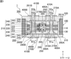
- FIG. 1 is a schematic cross-sectional view showing an example of a capacitor-embedded substrate according to a first embodiment of the present invention.
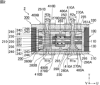
- FIG. 2 is a schematic cross-sectional view showing an example of a capacitor-embedded substrate according to a second embodiment of the present invention.
- FIG. 3 is a schematic cross-sectional view showing an example of a capacitor-embedded substrate according to a modified example of the second embodiment of the present invention.
- FIG. 4 is a schematic cross-sectional view showing an example of a capacitor-embedded substrate according to the third embodiment of the present invention.
- FIG. 5 is a schematic cross-sectional view showing an example of a capacitor-embedded substrate according to a fourth embodiment of the present invention.
- the capacitor-embedded substrate of the present invention will be described below. Note that the present invention is not limited to the configuration below, and may be modified as appropriate without departing from the gist of the present invention. In addition, a combination of multiple individual preferred configurations described below also constitutes the present invention.
- the capacitor-embedded substrate of the present invention comprises a core substrate having an opening in the thickness direction, a capacitor component provided in the opening of the core substrate, and a sealing material for sealing the core substrate and the capacitor component, the core substrate having a base material having the opening, the capacitor component comprising a capacitor body having an anode layer having a core, a dielectric layer, and a cathode layer facing the anode layer via the dielectric layer in the thickness direction, and a sealing material provided on at least the inner wall surface of a through hole penetrating the capacitor body in the thickness direction.
- the sealing material has a first sealing portion covering one surface of each of the core substrate and the capacitor component, and a second sealing portion covering the other surface of each of the core substrate and the capacitor component in the thickness direction, the one surface of the core substrate and the one surface of the capacitor component are on the same plane, and the diameter of the end of the through hole on the first sealing portion side is larger than the diameter of the end of the through hole on the second sealing portion side.
- FIG. 1 is a schematic cross-sectional view showing an example of a capacitor-embedded substrate according to a first embodiment of the present invention.
- the capacitor-embedded substrate 1 shown in FIG. 1 has a core substrate 100, a capacitor component 200, and a sealing material 300.
- the core substrate 100 has a base material 110.
- the core substrate 100 is composed only of the base material 110.
- the base material 110 has an opening (also called a cavity) 130 in the thickness direction T.
- the core substrate 100 has an opening 130.
- the opening 130 penetrates the core substrate 100, specifically, the base material 110, in the thickness direction T.
- the number of openings 130 provided in the core substrate 100 may be one or more.
- the substrate 110 is preferably made of an insulating material.
- the substrate 110 is preferably an insulating substrate.
- the insulating material constituting the substrate 110 may contain insulating resin, prepreg, inorganic material, a mixture of these, etc.
- Examples of insulating resins contained in the insulating material constituting the substrate 110 include epoxy resins, polyester resins, bismaleimide triazine resins, polyimide resins, phenolic resins, and allylated phenylene ether resins.
- Examples of prepregs contained in the insulating material that constitutes the base material 110 include resin-impregnated glass fibers (resin-impregnated glass cloth), etc.
- the diameter of the glass fiber (glass cloth) in the prepreg is 3 ⁇ m or more and 15 ⁇ m or less.
- the resin content in the prepreg is 50% by weight or more and 90% by weight or less.
- Examples of inorganic materials contained in the insulating material that constitutes the substrate 110 include glass.
- the capacitor component 200 is provided within the opening 130 of the core substrate 100.
- the capacitor components 200 may be provided in each of the openings 130, or the capacitor components 200 may be provided in some of the openings 130 while electronic components different from the capacitor components 200 are provided in the remaining openings 130.
- the capacitor component 200 has a capacitor body 210, a through conductor 260A, a through conductor 260B, a conductor wiring layer 270A, and a conductor wiring layer 270B.
- the capacitor body 210 has an anode layer 220, a dielectric layer 230, and a cathode layer 240.
- the capacitor body 210 constitutes an electrolytic capacitor. Note that the capacitor body 210 may also constitute a capacitor other than an electrolytic capacitor.
- the anode layer 220 has a core portion 221 and a porous portion 222.
- the core of the anode layer refers to a portion that is substantially free of pores such as a porous portion, and preferably constitutes the central portion in the thickness direction of the anode layer.
- the core 221 is preferably made of a metal, and more preferably made of a valve metal.
- the anode layer 220 is also called a valve metal substrate.
- valve metals constituting the core 221 include elemental metals such as aluminum, tantalum, niobium, titanium, and zirconium, and alloys containing at least one of these elemental metals. Among these, aluminum or an aluminum alloy is preferred.
- the porous portion 222 is provided on at least one of the two surfaces of the core portion 221 that face each other in the thickness direction T.
- the porous portion 222 may be provided only on one surface of the core portion 221, or on both surfaces of the core portion 221.
- the anode layer 220 has the porous portion 222 on at least one of the two surfaces that face each other in the thickness direction T. This increases the surface area of the anode layer 220, making it easier to improve the capacity of the capacitor body 210.
- the porous portion 222 is preferably an etching layer formed by etching the surface of the anode layer 220 (core portion 221).
- the shape of the anode layer 220 is preferably a flat plate (anode plate), and more preferably a foil (anode foil).
- plate-like shapes include foil-like, sheet-like, film-like, etc., and no distinction is made between these shapes based on the dimensions in the thickness direction.
- the dielectric layer 230 is provided on the surface of the porous portion 222. Specifically, the dielectric layer 230 is provided along the surface (contour) of each pore present in the porous portion 222.
- the dielectric layer 230 is preferably made of an oxide film of the valve metal described above.
- an oxide film that becomes the dielectric layer 230 is formed by anodizing the aluminum foil in an aqueous solution containing ammonium adipate or the like (also called chemical conversion treatment). Since the dielectric layer 230 is formed along the surface of the porous portion 222, the dielectric layer 230 has pores (recesses).
- the cathode layer 240 faces the anode layer 220 in the thickness direction T via the dielectric layer 230.
- the cathode layer 240 is disposed on the surface of the dielectric layer 230.
- the cathode layer 240 preferably has a solid electrolyte layer 241 provided on the surface of the dielectric layer 230, and a conductor layer 242 provided on the surface of the solid electrolyte layer 241.
- the capacitor body 210 constitutes a solid electrolytic capacitor.
- the solid electrolyte layer 241 preferably has an inner layer disposed inside the pores of the dielectric layer 230 and an outer layer covering the inner layer.
- Constituent materials for the solid electrolyte layer 241 include, for example, conductive polymers such as polypyrroles, polythiophenes, and polyanilines. Among these, polythiophenes are preferred, and poly(3,4-ethylenedioxythiophene) (PEDOT) is particularly preferred.
- the conductive polymer may also contain a dopant such as polystyrene sulfonate (PSS).
- the solid electrolyte layer 241 is formed in a predetermined area on the surface of the dielectric layer 230 by, for example, applying a dispersion of a conductive polymer such as poly(3,4-ethylenedioxythiophene) to the surface of the dielectric layer 230 and drying it, or by using a treatment liquid containing a polymerizable monomer such as 3,4-ethylenedioxythiophene to form a polymerized film of poly(3,4-ethylenedioxythiophene) on the surface of the dielectric layer 230.
- a conductive polymer such as poly(3,4-ethylenedioxythiophene)
- the conductive layer 242 preferably has a conductive resin layer 243 provided on the surface of the solid electrolyte layer 241 and a metal layer 244 provided on the surface of the conductive resin layer 243.
- the conductive resin layer 243 may be, for example, a conductive adhesive layer containing at least one conductive filler selected from the group consisting of copper filler, silver filler, nickel filler, and carbon filler.
- the metal layer 244 preferably contains a metal filler.
- the metal filler contained in the metal layer 244 is preferably at least one type selected from the group consisting of copper filler, silver filler, and nickel filler.
- the metal layer 244 may be, for example, a metal plating film, a metal foil, etc. In this case, it is preferable that the metal layer 244 is composed of at least one metal selected from the group consisting of copper, silver, nickel, and an alloy containing at least one of these metals as a main component.
- the main component means the elemental component with the largest weight percentage.
- the conductive layer 242 may have, for example, a carbon layer as the conductive resin layer 243 and a copper layer as the metal layer 244.
- the carbon layer is formed in a predetermined area by, for example, applying a carbon paste containing carbon filler to the surface of the solid electrolyte layer 241 using a sponge transfer method, a screen printing method, a dispenser coating method, an inkjet printing method, or the like.
- the copper layer is formed in a predetermined area by applying a copper paste containing copper filler to the surface of the carbon layer using a sponge transfer method, screen printing method, spray coating method, dispenser coating method, inkjet printing method, etc.
- the conductive layer 242 may have at least one of the conductive resin layer 243 and the metal layer 244. In other words, the conductive layer 242 may have only the conductive resin layer 243, may have only the metal layer 244, or may have both the conductive resin layer 243 and the metal layer 244.
- the capacitor body 210 further has a mask layer 250 provided on the periphery of the porous portion 222 when viewed from the thickness direction T.
- the mask layer 250 is preferably provided on the entire periphery of the porous portion 222 when viewed from the thickness direction T.
- the mask layer 250 may also be provided on only a portion of the periphery of the porous portion 222 when viewed from the thickness direction T.
- the mask layer 250 is preferably provided so as to extend inward from at least one of the two surfaces of the anode layer 220 in the thickness direction T, and more preferably so as to extend inward from both surfaces of the anode layer 220.
- the mask layer 250 may or may not be in contact with the core portion 221 in the thickness direction T.
- the mask layer 250 may be provided outside the porous portion 222 in addition to inside the porous portion 222. In this case, the mask layer 250 may be provided on the surface of the filled porous portion 222 while filling the inside of the porous portion 222. In other words, the thickness of the mask layer 250 may be greater than the thickness of the porous portion 222.
- the mask layer 250 is provided outside the porous portion 222, it is preferable that the mask layer 250 is provided in a region surrounding the cathode layer 240 when viewed from the thickness direction T.
- the mask layer 250 When viewed from the thickness direction T, the mask layer 250 may be partially overlapped with the cathode layer 240, or may not be entirely overlapped with the cathode layer 240.
- the mask layer 250 is preferably made of an insulating material. In this case, sufficient insulation between the anode layer 220 and the cathode layer 240 is ensured, and short circuits between the two are sufficiently prevented.
- Examples of insulating materials constituting the mask layer 250 include polyphenylsulfone (PPS), polyethersulfone (PES), cyanate ester resin, fluororesin (tetrafluoroethylene, tetrafluoroethylene-perfluoroalkylvinylether copolymer, etc.), a composition consisting of soluble polyimide siloxane and epoxy resin, polyimide resin, polyamideimide resin, derivatives or precursors of these, etc.
- PPS polyphenylsulfone
- PES polyethersulfone
- cyanate ester resin fluororesin (tetrafluoroethylene, tetrafluoroethylene-perfluoroalkylvinylether copolymer, etc.)
- fluororesin tetrafluoroethylene, tetrafluoroethylene-perfluoroalkylvinylether copolymer, etc.
- the mask layer 250 is formed on the periphery of the porous portion 222, for example, by applying the insulating material described above to positions on both surfaces of the anode layer 220 that overlap the periphery of the porous portion 222, and allowing the insulating material to penetrate from both surfaces of the anode layer 220 toward the inside.
- the mask layer 250 may be formed on the porous portion 222 either before the dielectric layer 230 or after the dielectric layer 230.
- the planar shape of the capacitor body 210 when viewed from the thickness direction T can be, for example, a rectangle (square or rectangle), a quadrangle other than a rectangle, a polygon such as a triangle, a pentagon, or a hexagon, a circle, an ellipse, etc.
- the number of capacitor bodies 210 in the capacitor component 200 may be one or more.
- the capacitor component 200 has a plurality of capacitor bodies 210
- the plurality of capacitor bodies 210 are arranged in a plane in a surface direction perpendicular to the thickness direction T.
- the surface direction is a direction that includes a first direction U perpendicular to the thickness direction T, and a second direction V perpendicular to the thickness direction T and the first direction U.
- the multiple capacitor bodies 210 When multiple capacitor bodies 210 are arranged in a plane in the planar direction, the multiple capacitor bodies 210 may be arranged in a plane along multiple directions in the planar direction, or may be arranged in a plane along one direction. Furthermore, the multiple capacitor bodies 210 may be arranged in a regular or irregular manner.
- the capacitor component 200 may form a capacitor array in which a plurality of capacitor bodies 210 are arranged in an array in the planar direction.
- the through conductor 260A is provided on at least the inner wall surface of the through hole 261A that penetrates at least the capacitor body 210 in the thickness direction T.
- the through hole 261A penetrates the capacitor body 210 and the sealing layer 290 described below in the thickness direction T.
- the through conductor 260A is provided on the inner wall surface of the through hole 261A.
- the through conductor 260A may be provided only on the inner wall surface of the through hole 261A, or may be provided throughout the entire interior of the through hole 261A.
- the capacitor component 200 may further have a resin filling portion 280A provided in the space surrounded by the through conductor 260A in the through hole 261A.
- the space in the through hole 261A is eliminated by providing the resin filling portion 280A, the occurrence of delamination of the through conductor 260A is suppressed.
- the thermal expansion coefficient of the resin-filled portion 280A is preferably higher than that of the through conductor 260A.
- the thermal expansion coefficient of the constituent material (resin material) of the resin-filled portion 280A is preferably higher than that of the constituent material of the through conductor 260A.
- the resin-filled portion 280A (specifically, the constituent material (resin material) of the resin-filled portion 280A) expands in a high-temperature environment, and the through conductor 260A is pressed against the inner wall surface of the through hole 261A from the inside to the outside of the through hole 261A, so that the occurrence of delamination of the through conductor 260A is sufficiently suppressed.
- the thermal expansion coefficient of the resin-filled portion 280A may be the same as the thermal expansion coefficient of the through conductor 260A, or may be lower than the thermal expansion coefficient of the through conductor 260A.
- the capacitor component 200 does not have to have the resin-filled portion 280A. In this case, it is preferable that the through conductor 260A is provided throughout the entire interior of the through hole 261A.
- the through conductor 260A is electrically connected to the anode layer 220.
- the through conductor 260A is preferably electrically connected to the end face of the anode layer 220 that faces the inner wall surface of the through hole 261A in the planar direction. In the example shown in FIG. 1, the through conductor 260A is directly connected to the end face of the anode layer 220.
- the core portion 221 and the porous portion 222 are exposed on the end face of the anode layer 220 that is electrically connected to the through conductor 260A.
- the porous portion 222 as well as the core portion 221 are electrically connected to the through conductor 260A.
- the through conductor 260A is electrically connected to the anode layer 220 around the entire circumference of the through hole 261A.
- the connection resistance between the anode layer 220 and the through conductor 260A is likely to decrease, and therefore the equivalent series resistance (ESR) of the capacitor component 200 is likely to decrease.
- the through conductor 260A may be electrically connected to the anode layer 220 via an anode connection layer.
- the anode connection layer is preferably provided between the anode layer 220 and the through conductor 260A in the planar direction.
- the anode connection layer functions as a barrier layer for the anode layer 220, specifically, as a barrier layer for the core portion 221 and the porous portion 222.
- the anode connection layer functions as a barrier layer for the anode layer 220, dissolution of the anode layer 220 that occurs during chemical treatment to form the conductor wiring layer 270A, etc. is suppressed, and thus the infiltration of the chemical solution into the capacitor body 210 is suppressed, which makes it easier to improve the reliability of the capacitor component 200.
- Examples of materials that can be used to form the through conductor 260A include metal materials that contain low-resistance metals such as copper, gold, and silver, and composite materials that combine the above metals with resin.
- the planar shape of the through hole 261A when viewed from the thickness direction T can be, for example, a circle, an ellipse, a rectangle (square or oblong), etc.
- the through conductor 260A is formed, for example, as follows. First, a through hole 261A is formed by performing laser processing or the like, which penetrates at least the capacitor body 210 in the thickness direction T. Then, the inner wall surface of the through hole 261A is metallized with a metal material containing a low-resistance metal such as copper, gold, or silver to form the through conductor 260A. When forming the through conductor 260A, for example, the inner wall surface of the through hole 261A may be metallized with an electroless copper plating process, an electrolytic copper plating process, or the like to facilitate processing.
- the method of forming the through conductor 260A may be a method of filling the through hole 261A with a metal material, a composite material of metal and resin, or the like, in addition to a method of metallizing the inner wall surface of the through hole 261A.
- the through conductor 260B is provided at least on the inner wall surface of the through hole 261B that penetrates at least the capacitor body 210 in the thickness direction T, at a position electrically insulated from the through conductor 260A.
- the through hole 261B penetrates the capacitor body 210 and the sealing layer 290 described below in the thickness direction T, at a position separated from the through hole 261A.
- the through conductor 260B is provided on the inner wall surface of the through hole 261B.
- the through conductor 260B may be provided only on the inner wall surface of the through hole 261B, or may be provided throughout the entire interior of the through hole 261B.
- the capacitor component 200 may further have a resin filling portion 280B provided in the space surrounded by the through conductor 260B in the through hole 261B.
- the space in the through hole 261B is eliminated by providing the resin filling portion 280B, the occurrence of delamination of the through conductor 260B is suppressed.
- the thermal expansion coefficient of the resin-filled portion 280B is preferably higher than that of the through conductor 260B.
- the thermal expansion coefficient of the constituent material (resin material) of the resin-filled portion 280B is preferably higher than that of the constituent material of the through conductor 260B.
- the resin-filled portion 280B (specifically, the constituent material (resin material) of the resin-filled portion 280B) expands in a high-temperature environment, and the through conductor 260B is pressed against the inner wall surface of the through hole 261B from the inside to the outside of the through hole 261B, so that the occurrence of delamination of the through conductor 260B is sufficiently suppressed.
- the thermal expansion coefficient of the resin-filled portion 280B may be the same as the thermal expansion coefficient of the through conductor 260B, or may be lower than the thermal expansion coefficient of the through conductor 260B.
- the capacitor component 200 does not have to have the resin-filled portion 280B. In this case, it is preferable that the through conductor 260B is provided throughout the entire interior of the through hole 261B.
- the through conductor 260B is preferably electrically connected to the cathode layer 240.
- the through conductor 260B is electrically connected to the cathode layer 240 via the conductor wiring layer 270B and a via conductor 285 described below.
- an insulating material such as a sealing layer 290 (described later) is filled between the capacitor body 210 and the through conductor 260B in the planar direction, and further between the anode layer 220 and the through conductor 260B in the planar direction.
- a sealing layer 290 (described later) is filled between the capacitor body 210 and the through conductor 260B in the planar direction, and further between the anode layer 220 and the through conductor 260B in the planar direction.
- Examples of materials that can be used to form the through conductor 260B include metal materials that contain low-resistance metals such as copper, gold, and silver, and composite materials that combine the above metals with resin.
- the constituent materials of the through conductor 260A and the through conductor 260B may be the same as each other or different from each other.
- the planar shape of the through hole 261B when viewed from the thickness direction T can be, for example, a circle, an ellipse, a rectangle (square or oblong), etc.
- planar shapes of through hole 261A and through hole 261B may be the same as each other or may be different from each other.
- the through conductor 260B is formed, for example, as follows. First, a through hole penetrating the capacitor body 210 in the thickness direction T is formed by performing laser processing or the like. Next, the capacitor body 210 is sealed using an insulating material or the like to form a sealing layer (for example, sealing layer 290 described later) that fills at least the above-mentioned through hole. Then, the above-mentioned sealing layer is formed by performing laser processing or the like on the above-mentioned sealing layer.
- a sealing layer for example, sealing layer 290 described later
- the diameter of the through hole 261B is made smaller than the diameter of the through hole formed earlier, so that the above-mentioned sealing layer is provided between the inner wall surface of the through hole formed earlier and the inner wall surface of the through hole 261B in the surface direction.
- the inner wall surface of the through hole 261B is metallized with a metal material containing a low-resistance metal such as copper, gold, or silver to form the through conductor 260B.
- the inner wall surface of the through hole 261B can be metallized by electroless copper plating, electrolytic copper plating, or the like to facilitate processing.
- the method of forming the through conductor 260B may be a method of filling the through hole 261B with a metal material, a composite material of metal and resin, or the like, in addition to a method of metallizing the inner wall surface of the through hole 261B.
- the conductor wiring layer 270A is provided on both ends of the through conductor 260A that face each other in the thickness direction T.
- the conductor wiring layer 270A is electrically connected to the through conductor 260A and functions as a connection terminal of the capacitor component 200.
- the conductor wiring layer 270A is electrically connected to the anode layer 220 via the through conductor 260A and functions as a connection terminal for the anode layer 220.
- the conductor wiring layer 270A may be made of a metal material containing a low-resistance metal such as copper, gold, or silver. In this case, the conductor wiring layer 270A is formed by plating both ends of the through conductor 260A, for example.
- a mixed material of at least one conductive filler selected from the group consisting of silver filler, copper filler, nickel filler, and carbon filler and resin may be used as the constituent material of the conductor wiring layer 270A.
- the conductor wiring layer 270B is provided on both ends of the through conductor 260B that face each other in the thickness direction T, in a position electrically insulated from the conductor wiring layer 270A.
- the conductor wiring layer 270B is electrically connected to the through conductor 260B and functions as a connection terminal for the capacitor component 200.
- the conductor wiring layer 270B is electrically connected to the cathode layer 240 through a via conductor 285 described below and functions as a connection terminal for the cathode layer 240.
- the conductor wiring layer 270B may be made of a metal material containing a low-resistance metal such as copper, gold, or silver. In this case, the conductor wiring layer 270B is formed by plating both ends of the through conductor 260B, for example.
- a mixed material of at least one conductive filler selected from the group consisting of silver filler, copper filler, nickel filler, and carbon filler, and resin may be used as the constituent material of the conductor wiring layer 270B.
- the constituent materials of the conductor wiring layer 270A and the conductor wiring layer 270B may be the same as each other or different from each other.
- the capacitor component 200 further includes a sealing layer 290 that seals the capacitor body 210.
- the capacitor body 210 is protected by the sealing layer 290.
- the sealing layer 290 preferably covers at least one of the two surfaces of the capacitor body 210 that face each other in the thickness direction T, and more preferably covers both surfaces of the capacitor body 210. In the example shown in FIG. 1, the sealing layer 290 covers the cathode layer 240 and the mask layer 250 that constitute both surfaces of the capacitor body 210.
- the sealing layer 290 overlaps the entire capacitor body 210 when viewed in the thickness direction T.
- the sealing layer 290 may penetrate the capacitor body 210 in the thickness direction T.
- the sealing layer 290 penetrates the anode layer 220, the dielectric layer 230, and the mask layer 250 in the thickness direction T.
- the sealing layer 290 is preferably provided between the capacitor body 210 and the through conductor 260B in the planar direction, and further between the anode layer 220 and the through conductor 260B in the planar direction.
- the sealing layer 290 is preferably in contact with both the capacitor body 210 and the through conductor 260B in the planar direction, and further with both the anode layer 220 and the through conductor 260B.
- the core portion 221 and the porous portion 222 are exposed on the end face of the anode layer 220 that is in contact with the sealing layer 290. This increases the contact area between the porous portion 222 and the sealing layer 290, improving adhesion between the two, and making it less likely that problems such as peeling between the porous portion 222 and the sealing layer 290 will occur.
- the mask layer 250 in which the constituent material of the mask layer 250 penetrates into the pores of the porous portion 222 and spreads inside the porous portion 222, is provided around the through conductor 260B.
- the insulation between the anode layer 220 and the through conductor 260B, and therefore the insulation between the anode layer 220 and the cathode layer 240, is sufficiently ensured, and short circuits between the two are sufficiently prevented.
- the constituent material of the sealing layer 290 penetrates into the pores of the porous portion 222.
- the mechanical strength of the porous portion 222 is improved, while the occurrence of delamination due to the pores in the porous portion 222 is suppressed.
- the thermal expansion coefficient of the sealing layer 290 is preferably higher than that of the through conductor 260B. Specifically, the thermal expansion coefficient of the constituent material of the sealing layer 290 is preferably higher than that of the constituent material of the through conductor 260B. In this case, the sealing layer 290 (specifically, the constituent material of the sealing layer 290) expands in a high-temperature environment, pressing down on the porous portion 222 and the through conductor 260B, thereby sufficiently suppressing the occurrence of delamination.
- the thermal expansion coefficient of the sealing layer 290 may be the same as that of the through conductor 260B, or may be lower than that of the through conductor 260B.
- the sealing layer 290 may be filled between adjacent capacitor bodies 210 so as to separate the multiple capacitor bodies 210 from each other.
- the sealing layer 290 is arranged to conform to the surface shape of the capacitor body 210.
- the through hole 261A penetrates the sealing layer 290 in the thickness direction T in addition to the capacitor body 210.
- the through hole 261A penetrates the capacitor body 210 and the sealing layer 290 in the thickness direction T.
- the through hole 261B penetrates the sealing layer 290 in the thickness direction T in addition to the capacitor body 210.
- the through hole 261B penetrates the capacitor body 210 and the sealing layer 290 in the thickness direction T.
- the conductor wiring layer 270A is preferably provided on both ends of the through conductor 260A as well as on both surfaces of the sealing layer 290 that face each other in the thickness direction T.
- the conductor wiring layer 270A is provided from both ends of the through conductor 260A to both surfaces of the sealing layer 290.
- the conductor wiring layer 270A is provided from one end of the through conductor 260A (the lower end in FIG. 1) to one surface of the sealing layer 290 (the lower surface in FIG. 1), and is provided from the other end of the through conductor 260A (the upper end in FIG. 1) to the other surface of the sealing layer 290 (the upper surface in FIG. 1).
- the conductor wiring layer 270B is preferably provided on both ends of the through conductor 260B as well as on both surfaces of the sealing layer 290 that face each other in the thickness direction T.
- the conductor wiring layer 270B is provided from both ends of the through conductor 260B to both surfaces of the sealing layer 290.
- the conductor wiring layer 270B is provided from one end of the through conductor 260B (the lower end in FIG. 1) to one surface of the sealing layer 290 (the lower surface in FIG. 1), and is provided from the other end of the through conductor 260B (the upper end in FIG. 1) to the other surface of the sealing layer 290 (the upper surface in FIG. 1).
- the sealing layer 290 is preferably made of an insulating material.
- the insulating material constituting the sealing layer 290 may contain an insulating resin.
- Examples of insulating resins contained in the insulating material that constitutes the sealing layer 290 include epoxy resin, phenolic resin, polyimide resin, etc.
- the insulating material constituting the sealing layer 290 may contain a filler.
- fillers contained in the insulating material that constitutes the sealing layer 290 include inorganic fillers such as silica filler and alumina filler.
- the sealing layer 290 may be composed of only one layer, or may be composed of multiple layers.
- the constituent materials of the multiple layers may be the same as each other, may be different from each other, or may be partially different.
- the sealing layer 290 is formed to seal the capacitor body 210, for example, by a method of thermocompressing an insulating resin sheet, or by applying an insulating resin paste and then thermally curing it.
- the capacitor component 200 preferably further includes a via conductor 285 that penetrates the sealing layer 290 in the thickness direction T and is connected to the cathode layer 240 and the conductor wiring layer 270B.
- Examples of materials that can be used to form the via conductor 285 include metal materials that contain low-resistance metals such as copper, gold, and silver.
- the via conductor 285 is formed, for example, by plating the inner wall surface of a through hole that penetrates the sealing layer 290 in the thickness direction T with the metal material described above, or by filling the through hole with a conductive paste and then performing a heat treatment.
- the sealing material 300 seals the core substrate 100 and the capacitor component 200.
- the sealing material 300 has a first sealing portion 310 and a second sealing portion 320 in the thickness direction T.
- the first sealing portion 310 covers one surface (the lower surface in FIG. 1) of each of the core substrate 100 and the capacitor component 200 in the thickness direction T.
- the second sealing portion 320 covers the other surface (the upper surface in FIG. 1) of each of the core substrate 100 and the capacitor component 200 in the thickness direction T.
- the sealing material 300 is provided between the core substrate 100 and the capacitor component 200 in the planar direction.
- the sealing material 300 may be integrated with the sealing layer 290 so that there is no interface between them, or may not be integrated with the sealing layer 290 so that there is an interface between them.
- the sealing material 300 is preferably made of an insulating material.
- the insulating material constituting the sealing material 300 may contain insulating resin, prepreg, inorganic material, a mixture of these, etc.
- Examples of insulating resins contained in the insulating material that constitutes the sealing material 300 include epoxy resin, phenolic resin, polyimide resin, etc.
- prepregs contained in the insulating material that constitutes the sealing material 300 include resin-impregnated glass fibers (resin-impregnated glass cloth), etc.
- the diameter of the glass fiber (glass cloth) in the prepreg is 3 ⁇ m or more and 15 ⁇ m or less.
- the prepreg contained in the insulating material that constitutes the sealing material 300 preferably has a resin content of 50% by weight or more and 90% by weight or less.
- Examples of inorganic materials contained in the insulating material that constitutes the sealing material 300 include glass.
- the constituent material of the sealing material 300 may be the same as the constituent material of the substrate 110, or it may be different.
- the diameter of the glass fibers (glass cloth) in the prepreg, the density of the glass fibers (glass cloth) in the prepreg, the resin content in the prepreg, etc. may be the same or different between the substrate 110 and the sealing material 300.
- the insulating material that constitutes the sealing material 300 may contain a filler.
- fillers contained in the insulating material that constitutes the sealing material 300 include inorganic fillers such as silica filler and alumina filler.
- the sealing material 300 may be composed of only one layer, or may be composed of multiple layers.
- the constituent materials of the multiple layers may be the same as each other, may be different from each other, or may be partially different.
- the sealing material 300 is formed to seal the core substrate 100 and the capacitor components 200, for example, by a method of thermocompressing an insulating resin sheet, or by applying an insulating resin paste and then thermally curing it.
- the capacitor-embedded substrate 1 is manufactured, for example, as follows. First, a core substrate 100 having an opening 130 in the thickness direction T and a capacitor component 200 are prepared. Next, the core substrate 100 is attached to the support tape from one surface (the lower surface in FIG. 1) to fix the core substrate 100 on the support tape. Next, the capacitor component 200 is inserted into the opening 130 of the core substrate 100 and pressed against the support tape exposed in the opening 130 of the core substrate 100 to fix the capacitor component 200 on the support tape. Then, a sealing material including a second sealing portion 320 is formed so as to seal the core substrate 100 and the capacitor component 200 from their other surfaces (the upper surface in FIG. 1) to the support tape, and the support tape is then removed.
- the core substrate 100 and the capacitor component 200 are sealed from one surface side (the lower surface in FIG. 1) and a sealing material including a first sealing portion 310 is formed so as to contact the previously formed sealing material, thereby obtaining the sealing material 300. In this manner, the capacitor-embedded substrate 1 is obtained.
- the capacitor-embedded substrate 1 When the capacitor-embedded substrate 1 is manufactured, for example, as described above, a characteristic positional relationship appears between the core substrate 100 and the capacitor component 200. That is, in the capacitor-embedded substrate 1, one surface of the core substrate 100 (the lower surface in FIG. 1) and one surface of the capacitor component 200 (the lower surface in FIG. 1) are on the same plane (on the dashed line in FIG. 1). Specifically, the surface of the core substrate 100 on the first sealing portion 310 side and the surface of the capacitor component 200 on the first sealing portion 310 side are on the same plane. In the example shown in FIG. 1, the surface of the core substrate 100 on the first sealing portion 310 side corresponds to the surface of the base material 110 on the first sealing portion 310 side. Also, in the example shown in FIG.
- the surface of the capacitor component 200 on the first sealing portion 310 side corresponds to the surfaces of the conductor wiring layer 270A and the conductor wiring layer 270B on the first sealing portion 310 side.
- the surface of the base material 110 facing the first sealing section 310 and the surfaces of the conductor wiring layer 270A and the conductor wiring layer 270B facing the first sealing section 310 are on the same plane.
- the diameter R1a (hereinafter simply referred to as diameter R1a) of the end of the through hole 261A on the first sealing portion 310 side is larger than the diameter R2a (hereinafter simply referred to as diameter R2a) of the end of the through hole 261A on the second sealing portion 320 side.
- the diameter R1b (hereinafter also simply referred to as diameter R1b) of the end of the through-hole 261B on the first sealing portion 310 side is larger than the diameter R2b (hereinafter also simply referred to as diameter R2b) of the end of the through-hole 261B on the second sealing portion 320 side.
- the pressure applied when the capacitor component 200 is pressed onto the support tape is applied to the conductor wiring layer 270A on the support tape side, i.e., the conductor wiring layer 270A on the first sealing portion 310 side.
- the diameter R1a of the through hole 261A is larger than the diameter R2a, so that the pressure applied to the conductor wiring layer 270A on the first sealing portion 310 side when the capacitor component 200 is pressed is dispersed, and therefore the conductor wiring layer 270A on the first sealing portion 310 side, and ultimately the through conductor 260A on whose end the conductor wiring layer 270A is provided, are less likely to be damaged by cracks, etc. Furthermore, in the capacitor-embedded substrate 1, as described above, the diameter R1a of the through hole 261A is larger than the diameter R2a.
- the diameter of the through hole 261A does not increase overall from the end on the first sealing portion 310 side to the end on the second sealing portion 320 side. This means that the area of the portion of the capacitor component 200 (capacitor body 210) that can exhibit capacitance does not decrease overall, and as a result, the decrease in the capacitance of the capacitor component 200 (capacitor body 210) is suppressed.
- the pressure applied when the capacitor component 200 is pressed onto the support tape is applied to the conductor wiring layer 270B on the support tape side, i.e., the conductor wiring layer 270B on the first sealing portion 310 side.
- the diameter R1b of the through hole 261B is larger than the diameter R2b, and therefore the pressure applied to the conductor wiring layer 270B on the first sealing portion 310 side when the capacitor component 200 is pressed is dispersed, so that the conductor wiring layer 270B on the first sealing portion 310 side, and ultimately the through conductor 260B on whose end the conductor wiring layer 270B is provided, are less likely to be damaged by cracks or the like.
- the diameter R1b of the through hole 261B is larger than the diameter R2b.
- the diameter of the through hole 261B does not increase overall from the end on the first sealing portion 310 side to the end on the second sealing portion 320 side. This means that the area of the portion of the capacitor component 200 (capacitor body 210) that can exhibit capacitance does not decrease overall, and as a result, the decrease in the capacitance of the capacitor component 200 (capacitor body 210) is suppressed.
- the capacitor-embedded substrate 1 can realize a capacitor-embedded substrate that can suppress both damage to the through conductors (in FIG. 1, through conductor 260A and through conductor 260B) and the conductor wiring layers (in FIG. 1, conductor wiring layer 270A and conductor wiring layer 270B) provided on the ends thereof, and a decrease in capacitance.
- the diameter of the end of the through hole on the first sealing portion side is determined by the equivalent circle diameter calculated from the area of that end when viewed from the thickness direction.
- the diameter of the end of the through hole on the second sealing portion side is determined by the equivalent circle diameter calculated from the area of that end when viewed from the thickness direction.
- both relationship A that is, "diameter R1a is larger than diameter R2a”
- relationship B that is, “diameter R1b is larger than diameter R2b”
- only relationship A may hold true
- only relationship B may hold true
- both relationship A and relationship B may hold true.
- the capacitor-embedded substrate of the present invention when there are multiple through holes in which a through conductor and a conductor wiring layer are provided, it is sufficient that the characteristic that "the diameter of the end of the through hole on the first sealing portion side is larger than the diameter of the end of the through hole on the second sealing portion side" is true for at least one of the multiple through holes, and it is particularly preferable that this characteristic is true for all of the through holes.
- the diameters R1a and R1b may be the same as each other or may be different from each other.
- the diameter R2a and the diameter R2b may be the same as each other or may be different from each other.
- the diameter R3a of the portion of through hole 261A that penetrates capacitor body 210 is smaller than the diameter R1a of the end of through hole 261A on the first sealing portion 310 side. In this case, the reduction in the area of the portion of capacitor component 200 (capacitor body 210) that can exhibit capacitance is sufficiently suppressed, and therefore the decrease in capacitance of capacitor component 200 (capacitor body 210) is sufficiently suppressed.
- the diameter R3b of the portion of through hole 261B that penetrates capacitor body 210 is smaller than the diameter R1b of the end of through hole 261B on the first sealing portion 310 side. In this case, the reduction in the area of the portion of capacitor component 200 (capacitor body 210) that can exhibit capacitance is sufficiently suppressed, and therefore the decrease in capacitance of capacitor component 200 (capacitor body 210) is sufficiently suppressed.
- the diameter R3a of the portion of through hole 261A penetrating capacitor body 210 is smaller than the diameter R1a of the end of through hole 261A on the first sealing portion 310 side and the diameter R2a of the end of through hole 261A on the second sealing portion 320 side. In this case, the reduction in the area of the portion of capacitor component 200 (capacitor body 210) that can exhibit capacitance is significantly suppressed, and therefore the decrease in capacitance of capacitor component 200 (capacitor body 210) is significantly suppressed.
- the diameter R3a of the portion of through hole 261A penetrating capacitor body 210 may be smaller than the diameter R1a of the end of through hole 261A on the first sealing portion 310 side, but larger than the diameter R2a of the end of through hole 261A on the second sealing portion 320 side.
- the diameter R3b of the portion of through hole 261B penetrating capacitor body 210 is smaller than the diameter R1b of the end of through hole 261B on the first sealing portion 310 side, but larger than the diameter R2b of the end of through hole 261B on the second sealing portion 320 side.
- the cross-sectional shape along the thickness direction T is not particularly limited.
- the cross-sectional shape of the through hole 261A may be, for example, a constricted shape in which the diameter is extremely small at the portion penetrating the capacitor body 210, or a tapered shape in which the diameter decreases from the end on the first sealing portion 310 side toward the end on the second sealing portion 320 side. In the example shown in FIG.
- the cross-sectional shape of the through hole 261A is the constricted shape described above, which is a preferred aspect from the viewpoint of suppressing a reduction in the area of the portion that can exhibit capacitance in the capacitor component 200 (capacitor body 210).
- the cross-sectional shape along the thickness direction T is not particularly limited.
- the cross-sectional shape of through hole 261B may be, for example, a constricted shape in which the diameter is extremely small at the portion penetrating capacitor body 210, or a tapered shape in which the diameter decreases from the end on the first sealing portion 310 side toward the end on the second sealing portion 320 side.
- the cross-sectional shape of through hole 261B is the tapered shape described above.
- cross-sectional shapes of through-hole 261A and through-hole 261B may be the same or different.
- the thickness of the core substrate 100 is preferably greater than the thickness of the capacitor component 200. In this case, when sealing the core substrate 100 and the capacitor component 200 with the sealing material 300, the pressure applied to the capacitor component 200 by the sealing material 300 is likely to be reduced, making it less likely that the capacitor component 200 will be damaged by the pressure.
- the linear expansion coefficient in the plane direction of the base material 110 is preferably 80% or more and 120% or less of the linear expansion coefficient in the plane direction of the sealing material 300.
- the stress applied to the capacitor component 200 from the core substrate 100 and the sealing material 300 is more likely to be reduced, making the capacitor component 200 less likely to be damaged by the above-mentioned stress.
- the thermal properties of the core substrate 100 and the sealing material 300 are more likely to be balanced, making it less likely that the capacitor-embedded substrate 1 will warp due to differences in thermal properties.
- the linear expansion coefficient of the base material 110 in the planar direction is 80% or more and 120% or less of the linear expansion coefficient of the sealing material 300 in the planar direction
- the linear expansion coefficient of the core portion 221 in the planar direction may be greater than 120% of the linear expansion coefficient of the sealing material 300 in the planar direction.
- the core substrate 100 and the sealing material 300 serve to restrain the capacitor component 200, so that the thermal expansion and thermal contraction of the capacitor component 200 are sufficiently suppressed, and as a result, damage to the through conductors (through conductors 260A and 260B in FIG. 1) and the conductor wiring layers (conductor wiring layers 270A and 270B in FIG. 1) provided on the ends thereof is sufficiently suppressed.
- the linear expansion coefficient in the plane direction of the base material 110 is not 80% or more and 120% or less of the linear expansion coefficient in the plane direction of the sealing material 300
- the linear expansion coefficient in the plane direction of the core 221 may be greater than 120% of the linear expansion coefficient in the plane direction of the sealing material 300.
- the sealing material 300 plays a role in restraining the capacitor component 200 during heat treatment of the capacitor-embedded substrate 1, so that the thermal expansion and thermal contraction of the capacitor component 200 is suppressed, and as a result, damage to the through conductors (through conductors 260A and 260B in FIG. 1) and the conductor wiring layers (conductor wiring layers 270A and 270B in FIG. 1) provided on the ends thereof is suppressed.
- the linear expansion coefficient in the plane direction of the base material 110 is 80% or more and 120% or less of the linear expansion coefficient in the plane direction of the sealing material 300
- the linear expansion coefficient in the plane direction of the core portion 221 may be 80% or more and 120% or less of the linear expansion coefficient in the plane direction of the sealing material 300.
- the stress applied to the capacitor component 200 from the core substrate 100 and the sealing material 300 is more likely to be reduced, making it less likely that the capacitor component 200 will be damaged by the above stress.
- the thermal properties of the core substrate 100, the capacitor component 200, and the sealing material 300 are more likely to be balanced, making it less likely that the capacitor-embedded substrate 1 will warp due to differences in thermal properties.
- the linear expansion coefficient in the plane direction of the base material 110 is not 80% or more and 120% or less of the linear expansion coefficient in the plane direction of the sealing material 300
- the linear expansion coefficient in the plane direction of the core portion 221 may be 80% or more and 120% or less of the linear expansion coefficient in the plane direction of the sealing material 300.
- the stress applied to the capacitor component 200 from the sealing material 300 is likely to be reduced, making the capacitor component 200 less likely to be damaged by the above-mentioned stress.
- the thermal properties of the capacitor component 200 and the sealing material 300 are likely to be balanced, making it less likely that the capacitor-embedded substrate 1 will warp due to differences in thermal properties.
- the linear expansion coefficient of the substrate 110 in the planar direction is the same as that of the sealing material 300 in the planar direction, and it is preferable that the linear expansion coefficient of the substrate 110 in the planar direction and the linear expansion coefficient of the sealing material 300 in the planar direction are smaller than the linear expansion coefficient of the core 221 in the planar direction.
- the core substrate 100 and the sealing material 300 play a role in restraining the capacitor component 200, so that the thermal expansion and thermal contraction of the capacitor component 200 are sufficiently suppressed, and as a result, damage to the through conductors (through conductors 260A and 260B in FIG. 1) and the conductor wiring layers (conductor wiring layers 270A and conductor wiring layers 270B in FIG. 1) provided on the ends thereof is sufficiently suppressed.
- the linear expansion coefficient of the substrate 110 in the planar direction is preferably smaller than that of the sealing material 300 in the planar direction, and the linear expansion coefficient of the sealing material 300 in the planar direction is preferably smaller than that of the core 221 in the planar direction.
- the curing temperature (e.g., heat curing temperature) of the sealing material 300 which has a larger linear expansion coefficient in the planar direction than the substrate 110, tends to be lower than the curing temperature (e.g., heat curing temperature) of the substrate 110.
- the core substrate 100 plays a role in restraining the capacitor component 200, and the capacitor component 200 is less likely to break down or deteriorate in characteristics due to heat when the sealing material 300 is cured (e.g., heat cured).
- the linear expansion coefficient in the planar direction of the target component of the capacitor-embedded board may be the linear expansion coefficient in any direction of the planar direction (e.g., the first direction U or the second direction V in Figure 1), and is determined by thermomechanical analysis (TMA) or dynamic mechanical analysis (DMA). If it is difficult to directly remove (extract) the target component from the capacitor-embedded board, a measuring component made of the same material as the target component may be prepared separately, and the linear expansion coefficient in the planar direction of the measuring component may be measured using the method described above.
- TMA thermomechanical analysis
- DMA dynamic mechanical analysis
- the capacitor-embedded substrate 1 may further include an external electrode layer 400A provided on both surfaces of the sealing material 300 facing each other in the thickness direction T and electrically connected to the conductor wiring layer 270A.
- the external electrode layer 400A functions as a connection terminal of the capacitor-embedded substrate 1.
- the external electrode layer 400A functions as a connection terminal for the conductor wiring layer 270A, and therefore as a connection terminal for the anode layer 220.
- Examples of materials that can be used to form the external electrode layer 400A include metal materials that contain low-resistance metals such as copper, gold, and silver.
- the capacitor-embedded substrate 1 may further include a via conductor 410A that penetrates the sealing material 300 in the thickness direction T and is connected to the conductor wiring layer 270A and the external electrode layer 400A.
- Examples of materials that can be used to form the via conductor 410A include metal materials that contain low-resistance metals such as copper, gold, and silver.
- the via conductor 410A is formed, for example, by plating the inner wall surface of a through hole that penetrates the sealing material 300 in the thickness direction T with the metal material described above, or by filling the hole with a conductive paste and then performing a heat treatment.
- the capacitor-embedded substrate 1 may further include an external electrode layer 400B provided on both surfaces of the sealing material 300 facing each other in the thickness direction T and electrically connected to the conductor wiring layer 270B.
- the external electrode layer 400B functions as a connection terminal of the capacitor-embedded substrate 1.
- the external electrode layer 400B functions as a connection terminal for the conductor wiring layer 270B, and therefore as a connection terminal for the cathode layer 240.
- Examples of materials that can be used to form the external electrode layer 400B include metal materials that contain low-resistance metals such as copper, gold, and silver.
- the constituent materials of the external electrode layer 400A and the external electrode layer 400B may be the same as or different from each other.
- the capacitor-embedded substrate 1 may further include a via conductor 410B that penetrates the sealing material 300 in the thickness direction T and is connected to the conductor wiring layer 270B and the external electrode layer 400B.
- Examples of materials that can be used to form the via conductor 410B include metal materials that contain low-resistance metals such as copper, gold, and silver.
- via conductor 410A and via conductor 410B may be the same as or different from each other.
- the via conductor 410B is formed, for example, by plating the inner wall surface of a through hole that penetrates the sealing material 300 in the thickness direction T with the metal material described above, or by filling the hole with a conductive paste and then performing a heat treatment.
- the capacitor component further includes a protective layer that covers at least a portion of at least one of the surfaces of the conductor wiring layer facing the first sealing portion and the second sealing portion.
- the capacitor-embedded substrate of embodiment 2 of the present invention is similar to the capacitor-embedded substrate of embodiment 1 of the present invention.
- FIG. 2 is a schematic cross-sectional view showing an example of a capacitor-embedded substrate according to embodiment 2 of the present invention.
- the capacitor component 200 further includes a protective layer 295.
- the protective layer 295 covers at least a portion of at least one of the surfaces of the conductor wiring layer 270A facing the first sealing portion 310 and the second sealing portion 320. In the example shown in FIG. 2, the protective layer 295 covers both the surface of the conductor wiring layer 270A facing the first sealing portion 310 and the surface of the conductor wiring layer 270A facing the second sealing portion 320. This protects the conductor wiring layer 270A with the protective layer 295.
- the pressure applied to the conductor wiring layer 270A on the first sealing portion 310 side is sufficiently dispersed, so that the conductor wiring layer 270A on the first sealing portion 310 side, and thus the through conductor 260A on whose end the conductor wiring layer 270A is provided, are less likely to be damaged.
- the protective layer 295 may be provided only on one of the surfaces of the conductor wiring layer 270A facing the first sealing section 310 and the surface facing the second sealing section 320.
- the protective layer 295 covers at least a portion of at least one of the surfaces of the conductor wiring layer 270B facing the first sealing portion 310 and the second sealing portion 320. In the example shown in FIG. 2, the protective layer 295 covers both the surface of the conductor wiring layer 270B facing the first sealing portion 310 and the surface of the conductor wiring layer 270B facing the second sealing portion 320. This protects the conductor wiring layer 270B with the protective layer 295.
- the pressure applied to the conductor wiring layer 270B on the first sealing portion 310 side is sufficiently dispersed, so that the conductor wiring layer 270B on the first sealing portion 310 side, and thus the through conductor 260B on whose end the conductor wiring layer 270B is provided, are less likely to be damaged.
- the protective layer 295 may be provided only on one of the surfaces of the conductor wiring layer 270B facing the first sealing section 310 and the surface facing the second sealing section 320.
- the protective layer 295 is preferably provided from the surface of the conductor wiring layer 270A facing the first sealing portion 310 to the surface of the conductor wiring layer 270B facing the first sealing portion 310.
- the protective layer 295 is preferably provided over the entire surfaces of the conductor wiring layer 270A and the conductor wiring layer 270B facing the first sealing portion 310.
- the protective layer 295 is preferably provided so as to cover the entire surfaces of the conductor wiring layer 270A and the conductor wiring layer 270B facing the first sealing portion 310.
- the protective layer 295 is preferably provided from the surface of the conductor wiring layer 270A facing the second sealing portion 320 to the surface of the conductor wiring layer 270B facing the second sealing portion 320.
- the protective layer 295 is preferably provided over the entire surfaces of the conductor wiring layer 270A and the conductor wiring layer 270B facing the second sealing portion 320.
- the protective layer 295 is preferably provided so as to cover the entire surfaces of the conductor wiring layer 270A and the conductor wiring layer 270B facing the second sealing portion 320.
- the protective layer 295 is particularly preferably provided from the surface of the conductor wiring layer 270A facing the first sealing portion 310 to the surface of the conductor wiring layer 270B facing the first sealing portion 310, and from the surface of the conductor wiring layer 270A facing the second sealing portion 320 to the surface of the conductor wiring layer 270B facing the second sealing portion 320.
- the protective layer 295 is provided over the entire surface of the conductor wiring layer 270A and the conductor wiring layer 270B facing the first sealing portion 310, and the entire surface of the conductor wiring layer 270A and the conductor wiring layer 270B facing the second sealing portion 320.
- the protective layer 295 is provided so as to cover the entire surface of the conductor wiring layer 270A and the conductor wiring layer 270B facing the first sealing portion 310, and the entire surface of the conductor wiring layer 270A and the conductor wiring layer 270B facing the second sealing portion 320.
- the protective layer 295 overlaps the entire capacitor body 210 when viewed in the thickness direction T.
- both ends of the protective layer 295 are located at the same positions as both ends of the capacitor body 210.
- one surface of the core substrate 100 (the lower surface in FIG. 2) and one surface of the capacitor component 200 (the lower surface in FIG. 2) are on the same plane (on the dashed line in FIG. 2).
- one surface of the core substrate 100, specifically, the surface of the core substrate 100 facing the first sealing portion 310 corresponds to the surface of the base material 110 facing the first sealing portion 310.
- one surface of the capacitor component 200, specifically, the surface of the capacitor component 200 facing the first sealing portion 310 corresponds to the surface of the protective layer 295 facing the first sealing portion 310.
- the surface of the base material 110 facing the first sealing portion 310 and the surface of the protective layer 295 facing the first sealing portion 310 are on the same plane.
- the linear expansion coefficient in the planar direction of the protective layer 295 is preferably 80% or more and 120% or less of the linear expansion coefficient in the planar direction of the core portion 221.
- the stress applied from the protective layer 295 to the conductor wiring layer (in FIG. 2, conductor wiring layer 270A and conductor wiring layer 270B), and in turn the stress applied from the protective layer 295 to the through conductor (in FIG. 2, through conductor 260A and through conductor 260B) is likely to be reduced, so that the through conductor (in FIG. 2, through conductor 260A and through conductor 260B) is less likely to be damaged by the above stress.
- the linear expansion coefficient of the protective layer 295 in the planar direction is 80% or more and 120% or less of the linear expansion coefficient of the core 221 in the planar direction
- the linear expansion coefficient of the protective layer 295 in the planar direction is preferably greater than 120% of the linear expansion coefficient of the sealing material 300 in the planar direction.
- the sealing material 300 plays a role in restraining the capacitor component 200 having the protective layer 295, so that the thermal expansion and thermal contraction of the capacitor component 200 having the protective layer 295 is suppressed, and as a result, damage to the through conductors (through conductors 260A and 260B in FIG. 2) and the conductor wiring layers (conductor wiring layers 270A and conductor wiring layers 270B in FIG. 2) provided on the ends thereof is suppressed.
- the linear expansion coefficient of the protective layer 295 in the planar direction is 80% or more and 120% or less of the linear expansion coefficient of the core 221 in the planar direction
- the linear expansion coefficient of the protective layer 295 in the planar direction is preferably greater than 120% of the linear expansion coefficient of the base material 110 in the planar direction.
- the core substrate 100 plays a role in restraining the capacitor component 200 having the protective layer 295, so that the thermal expansion and thermal contraction of the capacitor component 200 having the protective layer 295 is suppressed, and as a result, damage to the through conductors (through conductors 260A and 260B in FIG. 2) and the conductor wiring layers (conductor wiring layers 270A and 270B in FIG. 2) provided on the ends thereof is suppressed.
- the linear expansion coefficient of the protective layer 295 in the planar direction is 80% or more and 120% or less of the linear expansion coefficient of the core 221 in the planar direction, and is particularly preferably greater than 120% of the linear expansion coefficient of the sealing material 300 in the planar direction, and greater than 120% of the linear expansion coefficient of the base material 110 in the planar direction.
- the core substrate 100 and the sealing material 300 play a role in restraining the capacitor component 200 having the protective layer 295, so that the thermal expansion and thermal contraction of the capacitor component 200 having the protective layer 295 is sufficiently suppressed, and as a result, damage to the through conductor (in FIG. 2, the through conductor 260A and the through conductor 260B) and the conductor wiring layer (in FIG. 2, the conductor wiring layer 270A and the conductor wiring layer 270B) provided on the end of the through conductor is sufficiently suppressed.
- the linear expansion coefficient of the substrate 110 in the planar direction is the same as the linear expansion coefficient of the sealing material 300 in the planar direction, and the linear expansion coefficients of the substrate 110 in the planar direction and the sealing material 300 in the planar direction are smaller than the linear expansion coefficients of the core portion 221 in the planar direction, it is preferable that the linear expansion coefficient of the protective layer 295 in the planar direction is the same as the linear expansion coefficient of the substrate 110 in the planar direction and the sealing material 300 in the planar direction.
- the linear expansion coefficient of the substrate 110 in the planar direction, the linear expansion coefficient of the sealing material 300 in the planar direction, and the linear expansion coefficient of the protective layer 295 in the planar direction are the same as each other, and that the linear expansion coefficient of the substrate 110 in the planar direction, the linear expansion coefficient of the sealing material 300 in the planar direction, and the linear expansion coefficient of the protective layer 295 in the planar direction are smaller than the linear expansion coefficient of the core portion 221 in the planar direction.
- the stress applied to the capacitor component 200 from the core substrate 100 and the sealing material 300 is easily reduced, so that the capacitor component 200 is less likely to be damaged by the above stress.
- the stress applied from the protective layer 295 to the conductor wiring layer in FIG.
- the conductor wiring layer 270A and the conductor wiring layer 270B), and in turn, the stress applied from the protective layer 295 to the through conductor (in FIG. 2, the through conductor 260A and the through conductor 260B) is easily reduced, so that the through conductor (in FIG. 2, the through conductor 260A and the through conductor 260B) is less likely to be damaged by the above stress.
- the constituent material of the protective layer 295 is the same as the constituent material of the sealing material 300. In this case, processing and treatment of the sealing material 300 and the protective layer 295 are facilitated.
- the linear expansion coefficient of the substrate 110 in the planar direction is smaller than that of the sealing material 300 in the planar direction, and the linear expansion coefficient of the sealing material 300 in the planar direction is smaller than that of the core portion 221 in the planar direction, it is preferable that the linear expansion coefficient of the protective layer 295 in the planar direction is the same as that of the substrate 110 in the planar direction.
- the linear expansion coefficient of the substrate 110 in the planar direction and the linear expansion coefficient of the protective layer 295 in the planar direction are the same, and that the linear expansion coefficient of the substrate 110 in the planar direction and the linear expansion coefficient of the protective layer 295 in the planar direction are smaller than that of the sealing material 300 in the planar direction, and that the linear expansion coefficient of the sealing material 300 in the planar direction is smaller than that of the core portion 221 in the planar direction.
- the core substrate 100 restrains the capacitor component 200
- the protective layer 295 restrains the capacitor component 200 other than the protective layer 295, so that the thermal expansion and contraction of the capacitor component 200 is sufficiently suppressed.
- the constituent material of the protective layer 295 is the same as that of the sealing material 300. In this case, processing and treatment of the sealing material 300 and the protective layer 295 are facilitated.
- the via conductors 410A and 410B it becomes easier to perform laser processing for forming through holes penetrating the sealing material 300 and the protective layer 295 in the thickness direction T, desmear processing for removing residues generated during the laser processing, plating processing for plating the inner wall surface of the through holes with a metal material, etc.
- the protective layer 295 is preferably made of an insulating material.
- the insulating material constituting the protective layer 295 may contain insulating resin, prepreg, inorganic material, a mixture of these, etc.
- Examples of insulating resins contained in the insulating material that constitutes the protective layer 295 include epoxy resin, phenolic resin, polyimide resin, etc.
- prepregs contained in the insulating material that constitutes the protective layer 295 include resin-impregnated glass fiber (resin-impregnated glass cloth), etc.
- the diameter of the glass fiber (glass cloth) in the prepreg is 3 ⁇ m or more and 15 ⁇ m or less.
- the prepreg contained in the insulating material that constitutes the protective layer 295 preferably has a resin content of 50% by weight or more and 90% by weight or less.
- Examples of inorganic materials contained in the insulating material that constitutes the protective layer 295 include glass.
- the material of the protective layer 295 may be the same as or different from the material of the substrate 110.
- the diameter of the glass fibers (glass cloth) in the prepreg, the density of the glass fibers (glass cloth) in the prepreg, the resin content in the prepreg, etc. may be the same or different between the base material 110 and the protective layer 295.
- the constituent material of the protective layer 295 may be the same as or different from the constituent material of the sealing material 300.
- processing, treatment, etc. of the sealing material 300 and the protective layer 295 are facilitated.
- the diameter of the glass fibers (glass cloth) in the prepreg, the density of the glass fibers (glass cloth) in the prepreg, the resin content in the prepreg, etc. may be the same or different between the sealing material 300 and the protective layer 295.
- the same protective layer 295 may be composed of only one layer, or may be composed of multiple layers.
- the constituent materials of the multiple layers may be the same as each other, may be different from each other, or may be partially different.
- the protective layer 295 is formed so as to cover at least a portion of at least one of the surfaces of the conductor wiring layer 270A facing the first sealing portion 310 and the second sealing portion 320, by, for example, a method of thermocompressing an insulating resin sheet, or a method of applying an insulating resin paste and then thermally curing it.
- the protective layer 295 may have an opening in the thickness direction T, and the opening in the protective layer 295 may be filled with a sealing material 300.
- FIG. 3 is a schematic cross-sectional view showing an example of a capacitor-embedded substrate according to a modified example of embodiment 2 of the present invention.
- the protective layer 295 has an opening 296 in the thickness direction T.
- the opening 296 penetrates the protective layer 295 in the thickness direction T. That is, in the example shown in FIG. 3, the protective layer 295 has an opening 296 in the thickness direction T so that a portion of each of the conductor wiring layer 270A and the conductor wiring layer 270B is exposed.
- the opening 296 of the protective layer 295 is filled with a sealing material 300.
- a sealing material 300 In the example shown in FIG. 3, each part of the conductor wiring layer 270A and the conductor wiring layer 270B exposed in the opening 296 of the protective layer 295 is covered with the sealing material 300 filled in the opening 296 of the protective layer 295. This increases the contact area of the sealing material 300 with the capacitor component 200, improving the adhesion of the sealing material 300 to the capacitor component 200.
- the opening 296 does not have to penetrate the protective layer 295 in the thickness direction T.
- the conductor wiring layer 270A or the conductor wiring layer 270B does not have to be exposed in the opening 296 of the protective layer 295.
- the opening 296 of the protective layer 295 may be hole-shaped (hole-shaped) or slit-shaped (groove-shaped) when viewed from the thickness direction T.
- the number of openings 296 provided in the same protective layer 295 may be one or more.
- the multiple openings 296 may be arranged regularly or irregularly when viewed from the thickness direction T.
- the core substrate further has an electrode provided on at least one of the surface on the first sealing portion side and the surface on the second sealing portion side of the base material.
- the capacitor-embedded substrate of embodiment 3 of the present invention is similar to the capacitor-embedded substrate of embodiment 1 of the present invention.
- FIG. 4 is a schematic cross-sectional view showing an example of a capacitor-embedded substrate according to embodiment 3 of the present invention.
- the core substrate 100 further has an electrode 120.
- the electrode 120 is provided on at least one of the surfaces of the substrate 110 facing the first sealing portion 310 (the lower surface in FIG. 4) and the surface of the substrate 110 facing the second sealing portion 320 (the upper surface in FIG. 4). In the example shown in FIG. 4, the electrode 120 is provided on both the surface of the substrate 110 facing the first sealing portion 310 and the surface of the substrate 110 facing the second sealing portion 320.
- the electrode 120 may be provided on only one of the surfaces of the substrate 110 facing the first sealing portion 310 and the surface facing the second sealing portion 320.
- Examples of materials that can be used to construct the electrode 120 include metal materials that contain low-resistance metals such as copper, gold, and silver.
- one surface of the core substrate 100 (the lower surface in FIG. 4) and one surface of the capacitor component 200 (the lower surface in FIG. 4) are on the same plane (on the dashed line in FIG. 4).
- one surface of the core substrate 100, specifically, the surface of the core substrate 100 facing the first sealing portion 310 corresponds to the surface of the electrode 120 facing the first sealing portion 310.
- one surface of the capacitor component 200, specifically, the surface of the capacitor component 200 facing the first sealing portion 310 corresponds to the surfaces of the conductor wiring layer 270A and the conductor wiring layer 270B facing the first sealing portion 310.
- the surface of the electrode 120 facing the first sealing portion 310 and the surfaces of the conductor wiring layer 270A and the conductor wiring layer 270B facing the first sealing portion 310 are on the same plane.
- the capacitor component further has a protective layer covering at least a portion of at least one of the surfaces of the conductor wiring layer facing the first sealing portion and the second sealing portion
- the core substrate further has an electrode provided on at least one of the surfaces of the base material facing the first sealing portion and the second sealing portion.
- capacitor-embedded substrate of embodiment 4 of the present invention is similar to the capacitor-embedded substrate of embodiment 1 of the present invention.
- FIG. 5 is a schematic cross-sectional view showing an example of a capacitor-embedded substrate according to embodiment 4 of the present invention.
- the capacitor component 200 further includes a protective layer 295.
- the configuration of the protective layer 295 in the capacitor-embedded substrate 4 may be the same as the configuration of the protective layer 295 in the capacitor-embedded substrate 2 (see FIG. 2).
- the protective layer 295 in the capacitor-embedded substrate 4, may have an opening in the thickness direction T, and further, the opening of the protective layer 295 may be filled with a sealant 300.
- the configuration of the opening of such a protective layer 295 may be the same as the configuration of the opening 296 of the protective layer 295 in the capacitor-embedded substrate 2' (see FIG. 3).
- the core substrate 100 further has an electrode 120.
- the configuration of the electrodes 120 in the capacitor-embedded substrate 4 may be the same as the configuration of the electrodes 120 in the capacitor-embedded substrate 3 (see FIG. 4).
- one surface of the core substrate 100 (the lower surface in FIG. 5) and one surface of the capacitor component 200 (the lower surface in FIG. 5) are on the same plane (on the dashed line in FIG. 5).
- one surface of the core substrate 100, specifically, the surface of the core substrate 100 facing the first sealing portion 310 corresponds to the surface of the electrode 120 facing the first sealing portion 310.
- one surface of the capacitor component 200, specifically, the surface of the capacitor component 200 facing the first sealing portion 310 corresponds to the surface of the protective layer 295 facing the first sealing portion 310.
- the surface of the electrode 120 facing the first sealing portion 310 and the surface of the protective layer 295 facing the first sealing portion 310 are on the same plane.
- the capacitor component (capacitor body) is not limited to an electrolytic capacitor including the above-mentioned solid electrolytic capacitor.
- the capacitor component (capacitor body) may be, for example, a ceramic capacitor using barium titanate, a thin-film capacitor using silicon nitride (SiN), silicon dioxide (SiO 2 ), hydrogen fluoride (HF), or the like, or a trench-type capacitor having a metal insulator metal (MIM) structure.
- the capacitor components constitute a capacitor whose base material is a metal such as aluminum, and it is even more preferable that the capacitor components constitute an electrolytic capacitor whose base material is a metal such as aluminum.
- the capacitor-embedded substrate of the present invention may be used, for example, in a composite electronic component.
- a composite electronic component has, for example, the capacitor-embedded substrate of the present invention and an electronic component electrically connected to the capacitor-embedded substrate of the present invention (for example, an external electrode layer).
- the electronic components used in a composite electronic component may be passive elements, active elements, both passive and active elements, or a composite of passive and active elements.
- An example of a passive element is an inductor.
- Active elements include memory, GPU (Graphical Processing Unit), CPU (Central Processing Unit), MPU (Micro Processing Unit), PMIC (Power Management IC), etc.
- the capacitor-embedded board of the present invention is used in a composite electronic component
- the capacitor-embedded board of the present invention is treated, for example, as a board for mounting electronic components.
- the capacitor-embedded board of the present invention by forming the capacitor-embedded board of the present invention as a whole in a sheet shape, and further forming the electronic components to be mounted on the capacitor-embedded board of the present invention in a sheet shape, it becomes possible to electrically connect the capacitor-embedded board of the present invention and the electronic components in the thickness direction via the through conductors that penetrate the electronic components in the thickness direction.
- a switching regulator can be formed by electrically connecting the capacitor element of the present invention between a voltage regulator including a semiconductor active element and a load to which the converted DC voltage is supplied.
- a circuit layer may be formed on the sealing material of the capacitor-embedded substrate of the present invention, and the circuit layer may then be electrically connected to a passive element or active element as an electronic component.
- a core substrate having an opening in a thickness direction; a capacitor component provided in the opening of the core substrate; a sealing material that seals the core substrate and the capacitor component, the core substrate has a base material in which the opening is provided
- the capacitor component includes a capacitor body having an anode layer having a core, a dielectric layer, and a cathode layer facing the anode layer with the dielectric layer interposed therebetween in the thickness direction, a through conductor provided on at least an inner wall surface of a through hole penetrating at least the capacitor body in the thickness direction, and a conductor wiring layer provided on both ends of the through conductor facing each other in the thickness direction
- the sealing material has, in the thickness direction, a first sealing portion covering one surface of each of the core substrate and the capacitor component, and a second sealing portion covering the other surface of each of the core substrate and the capacitor component, the one surface of the core substrate and the one surface of the capacitor component are on the same plane, the diameter of the through hole at the end portion on the first sealing portion
- ⁇ 2> The capacitor-embedded substrate according to ⁇ 1>, wherein a diameter of the through hole at a portion passing through the capacitor body is smaller than a diameter of an end of the through hole on the first sealing portion side.
- ⁇ 3> The capacitor-embedded substrate described in ⁇ 2>, wherein the diameter of the portion of the through hole that penetrates the capacitor body is smaller than the diameter of the end of the through hole on the first sealing portion side and the diameter of the end of the through hole on the second sealing portion side.
- ⁇ 4> The capacitor-embedded substrate according to any one of ⁇ 1> to ⁇ 3>, wherein the thickness of the core substrate is greater than the thickness of the capacitor component.
- ⁇ 5> The capacitor-embedded substrate according to any one of ⁇ 1> to ⁇ 4>, wherein the base has a linear expansion coefficient in a plane direction perpendicular to the thickness direction, which is 80% or more and 120% or less of the linear expansion coefficient in the plane direction of the sealing material.
- ⁇ 6> The capacitor-embedded substrate according to any one of ⁇ 1> to ⁇ 5>, wherein a linear expansion coefficient of the core in a surface direction perpendicular to the thickness direction is greater than 120% of a linear expansion coefficient of the sealing material in the surface direction.
- ⁇ 7> The capacitor-embedded substrate according to any one of ⁇ 1> to ⁇ 5>, wherein a linear expansion coefficient of the core in a surface direction perpendicular to the thickness direction is 80% or more and 120% or less of a linear expansion coefficient of the sealing material in the surface direction.
- ⁇ 8> The capacitor-embedded substrate according to any one of ⁇ 1> to ⁇ 7>, wherein the capacitor component further has a protective layer covering at least a portion of at least one of a surface of the conductor wiring layer facing the first sealing portion and a surface of the conductor wiring layer facing the second sealing portion.
- ⁇ 10> The capacitor-embedded substrate according to ⁇ 9>, wherein a linear expansion coefficient of the protective layer in the plane direction is greater than 120% of a linear expansion coefficient of the sealing material in the plane direction.
- the protective layer has an opening in the thickness direction,
- the capacitor-embedded substrate according to any one of ⁇ 8> to ⁇ 11>, wherein the opening in the protective layer is filled with the sealing material.
- ⁇ 13> The capacitor-embedded substrate according to any one of ⁇ 1> to ⁇ 12>, wherein the core substrate further has an electrode provided on at least one of a surface of the base material facing the first sealing portion and a surface of the base material facing the second sealing portion.
- the anode layer has the core portion and a porous portion provided on at least one of both surfaces of the core portion facing each other in the thickness direction, the dielectric layer is provided on a surface of the porous portion,
- the capacitor-embedded substrate according to any one of ⁇ 1> to ⁇ 13>, wherein the cathode layer is provided on a surface of the dielectric layer.
- Capacitor-embedded substrate 100 Core substrate 110 Base material 120 Electrode 130 Opening (cavity) 200 Capacitor component 210 Capacitor body 220 Anode layer 221 Core 222 Porous portion 230 Dielectric layer 240 Cathode layer 241 Solid electrolyte layer 242 Conductor layer 243 Conductive resin layer 244 Metal layer 250 Mask layer 260A, 260B Through conductor 261A, 261B Through hole 270A, 270B Conductor wiring layer 280A, 280B Resin filling portion 285, 410A, 410B Via conductor 290 Sealing layer 295 Protective layer 296 Opening 300 Sealing material 310 First sealing portion 320 Second sealing portion 400A, 400B External electrode layer R1a, R1b Diameter R2a, R2b of end of through hole on first sealing portion side Diameter R3a, R3b of end of through hole on second sealing portion side Diameter T of the through hole penetrating the capacitor body Thickness direction U First direction V
Landscapes
- Engineering & Computer Science (AREA)
- Power Engineering (AREA)
- Microelectronics & Electronic Packaging (AREA)
- Manufacturing & Machinery (AREA)
- Fixed Capacitors And Capacitor Manufacturing Machines (AREA)
Priority Applications (3)
| Application Number | Priority Date | Filing Date | Title |
|---|---|---|---|
| CN202480003594.3A CN119631583A (zh) | 2023-03-09 | 2024-02-27 | 电容器内置基板 |
| JP2024559680A JP7816563B2 (ja) | 2023-03-09 | 2024-02-27 | コンデンサ内蔵基板 |
| US19/027,718 US20250174397A1 (en) | 2023-03-09 | 2025-01-17 | Capacitor embedded substrate |
Applications Claiming Priority (2)
| Application Number | Priority Date | Filing Date | Title |
|---|---|---|---|
| JP2023-036657 | 2023-03-09 | ||
| JP2023036657 | 2023-03-09 |
Related Child Applications (1)
| Application Number | Title | Priority Date | Filing Date |
|---|---|---|---|
| US19/027,718 Continuation US20250174397A1 (en) | 2023-03-09 | 2025-01-17 | Capacitor embedded substrate |
Publications (1)
| Publication Number | Publication Date |
|---|---|
| WO2024185585A1 true WO2024185585A1 (ja) | 2024-09-12 |
Family
ID=92674836
Family Applications (1)
| Application Number | Title | Priority Date | Filing Date |
|---|---|---|---|
| PCT/JP2024/007030 Ceased WO2024185585A1 (ja) | 2023-03-09 | 2024-02-27 | コンデンサ内蔵基板 |
Country Status (4)
| Country | Link |
|---|---|
| US (1) | US20250174397A1 (https=) |
| JP (1) | JP7816563B2 (https=) |
| CN (1) | CN119631583A (https=) |
| WO (1) | WO2024185585A1 (https=) |
Citations (3)
| Publication number | Priority date | Publication date | Assignee | Title |
|---|---|---|---|---|
| JP2010021369A (ja) * | 2008-07-10 | 2010-01-28 | Ngk Spark Plug Co Ltd | 部品内蔵配線基板及びその製造方法 |
| JP7143966B2 (ja) * | 2020-05-28 | 2022-09-29 | 株式会社村田製作所 | モジュール |
| WO2023021881A1 (ja) * | 2021-08-18 | 2023-02-23 | 株式会社村田製作所 | コンデンサ素子 |
-
2024
- 2024-02-27 WO PCT/JP2024/007030 patent/WO2024185585A1/ja not_active Ceased
- 2024-02-27 JP JP2024559680A patent/JP7816563B2/ja active Active
- 2024-02-27 CN CN202480003594.3A patent/CN119631583A/zh active Pending
-
2025
- 2025-01-17 US US19/027,718 patent/US20250174397A1/en active Pending
Patent Citations (3)
| Publication number | Priority date | Publication date | Assignee | Title |
|---|---|---|---|---|
| JP2010021369A (ja) * | 2008-07-10 | 2010-01-28 | Ngk Spark Plug Co Ltd | 部品内蔵配線基板及びその製造方法 |
| JP7143966B2 (ja) * | 2020-05-28 | 2022-09-29 | 株式会社村田製作所 | モジュール |
| WO2023021881A1 (ja) * | 2021-08-18 | 2023-02-23 | 株式会社村田製作所 | コンデンサ素子 |
Also Published As
| Publication number | Publication date |
|---|---|
| JPWO2024185585A1 (https=) | 2024-09-12 |
| US20250174397A1 (en) | 2025-05-29 |
| CN119631583A (zh) | 2025-03-14 |
| JP7816563B2 (ja) | 2026-02-18 |
Similar Documents
| Publication | Publication Date | Title |
|---|---|---|
| JP7597277B2 (ja) | コンデンサアレイ | |
| JP7732589B2 (ja) | コンデンサ | |
| JP7816633B2 (ja) | コンデンサ内蔵基板 | |
| US20250273405A1 (en) | Capacitor element | |
| US20250166927A1 (en) | Capacitor element | |
| US20250104932A1 (en) | Capacitor element | |
| CN223785015U (zh) | 电容器元件 | |
| JP7816563B2 (ja) | コンデンサ内蔵基板 | |
| TWI858676B (zh) | 電容器陣列 | |
| TWI831226B (zh) | 電容器 | |
| US20250357053A1 (en) | Capacitor element | |
| US20250201486A1 (en) | Capacitor embedded substrate | |
| JP7622919B1 (ja) | コンデンサ素子製造用基板及びコンデンサ素子の製造方法 | |
| US20250087429A1 (en) | Capacitor array | |
| WO2026079126A1 (ja) | 電子部品 | |
| WO2026048934A1 (ja) | コンデンサ素子 | |
| WO2026048931A1 (ja) | コンデンサ素子 | |
| WO2024214424A1 (ja) | コンデンサ素子 | |
| WO2024247589A1 (ja) | コンデンサ素子 | |
| WO2026048925A1 (ja) | コンデンサ素子 | |
| TW202518959A (zh) | 內建電容器之基板 | |
| WO2025243714A1 (ja) | コンデンサ素子 |
Legal Events
| Date | Code | Title | Description |
|---|---|---|---|
| WWE | Wipo information: entry into national phase |
Ref document number: 2024559680 Country of ref document: JP |
|
| 121 | Ep: the epo has been informed by wipo that ep was designated in this application |
Ref document number: 24766956 Country of ref document: EP Kind code of ref document: A1 |
|
| WWE | Wipo information: entry into national phase |
Ref document number: 202480003594.3 Country of ref document: CN |
|
| WWP | Wipo information: published in national office |
Ref document number: 202480003594.3 Country of ref document: CN |
|
| NENP | Non-entry into the national phase |
Ref country code: DE |
|
| 122 | Ep: pct application non-entry in european phase |
Ref document number: 24766956 Country of ref document: EP Kind code of ref document: A1 |