WO2024185478A1 - 検出装置 - Google Patents
検出装置 Download PDFInfo
- Publication number
- WO2024185478A1 WO2024185478A1 PCT/JP2024/005911 JP2024005911W WO2024185478A1 WO 2024185478 A1 WO2024185478 A1 WO 2024185478A1 JP 2024005911 W JP2024005911 W JP 2024005911W WO 2024185478 A1 WO2024185478 A1 WO 2024185478A1
- Authority
- WO
- WIPO (PCT)
- Prior art keywords
- organic
- buffer layer
- light
- electrode
- detection
- Prior art date
- Legal status (The legal status is an assumption and is not a legal conclusion. Google has not performed a legal analysis and makes no representation as to the accuracy of the status listed.)
- Ceased
Links
Images




Classifications
-
- H—ELECTRICITY
- H10—SEMICONDUCTOR DEVICES; ELECTRIC SOLID-STATE DEVICES NOT OTHERWISE PROVIDED FOR
- H10K—ORGANIC ELECTRIC SOLID-STATE DEVICES
- H10K39/00—Integrated devices, or assemblies of multiple devices, comprising at least one organic radiation-sensitive element covered by group H10K30/00
- H10K39/601—Assemblies of multiple devices comprising at least one organic radiation-sensitive element
-
- A—HUMAN NECESSITIES
- A61—MEDICAL OR VETERINARY SCIENCE; HYGIENE
- A61B—DIAGNOSIS; SURGERY; IDENTIFICATION
- A61B5/00—Measuring for diagnostic purposes; Identification of persons
- A61B5/02—Detecting, measuring or recording for evaluating the cardiovascular system, e.g. pulse, heart rate, blood pressure or blood flow
-
- A—HUMAN NECESSITIES
- A61—MEDICAL OR VETERINARY SCIENCE; HYGIENE
- A61B—DIAGNOSIS; SURGERY; IDENTIFICATION
- A61B5/00—Measuring for diagnostic purposes; Identification of persons
- A61B5/103—Measuring devices for testing the shape, pattern, colour, size or movement of the body or parts thereof, for diagnostic purposes
- A61B5/107—Measuring physical dimensions, e.g. size of the entire body or parts thereof
-
- A—HUMAN NECESSITIES
- A61—MEDICAL OR VETERINARY SCIENCE; HYGIENE
- A61B—DIAGNOSIS; SURGERY; IDENTIFICATION
- A61B5/00—Measuring for diagnostic purposes; Identification of persons
- A61B5/145—Measuring characteristics of blood in vivo, e.g. gas concentration or pH-value ; Measuring characteristics of body fluids or tissues, e.g. interstitial fluid or cerebral tissue
- A61B5/1455—Measuring characteristics of blood in vivo, e.g. gas concentration or pH-value ; Measuring characteristics of body fluids or tissues, e.g. interstitial fluid or cerebral tissue using optical sensors, e.g. spectral photometrical oximeters
-
- G—PHYSICS
- G06—COMPUTING OR CALCULATING; COUNTING
- G06F—ELECTRIC DIGITAL DATA PROCESSING
- G06F1/00—Details not covered by groups G06F3/00 - G06F13/00 and G06F21/00
- G06F1/16—Constructional details or arrangements
- G06F1/1613—Constructional details or arrangements for portable computers
- G06F1/163—Wearable computers, e.g. on a belt
-
- G—PHYSICS
- G06—COMPUTING OR CALCULATING; COUNTING
- G06F—ELECTRIC DIGITAL DATA PROCESSING
- G06F1/00—Details not covered by groups G06F3/00 - G06F13/00 and G06F21/00
- G06F1/16—Constructional details or arrangements
- G06F1/1613—Constructional details or arrangements for portable computers
- G06F1/1633—Constructional details or arrangements of portable computers not specific to the type of enclosures covered by groups G06F1/1615 - G06F1/1626
- G06F1/1635—Details related to the integration of battery packs and other power supplies such as fuel cells or integrated AC adapter
-
- H—ELECTRICITY
- H10—SEMICONDUCTOR DEVICES; ELECTRIC SOLID-STATE DEVICES NOT OTHERWISE PROVIDED FOR
- H10F—INORGANIC SEMICONDUCTOR DEVICES SENSITIVE TO INFRARED RADIATION, LIGHT, ELECTROMAGNETIC RADIATION OF SHORTER WAVELENGTH OR CORPUSCULAR RADIATION
- H10F39/00—Integrated devices, or assemblies of multiple devices, comprising at least one element covered by group H10F30/00, e.g. radiation detectors comprising photodiode arrays
- H10F39/10—Integrated devices
- H10F39/12—Image sensors
-
- H—ELECTRICITY
- H10—SEMICONDUCTOR DEVICES; ELECTRIC SOLID-STATE DEVICES NOT OTHERWISE PROVIDED FOR
- H10K—ORGANIC ELECTRIC SOLID-STATE DEVICES
- H10K39/00—Integrated devices, or assemblies of multiple devices, comprising at least one organic radiation-sensitive element covered by group H10K30/00
- H10K39/10—Organic photovoltaic [PV] modules; Arrays of single organic PV cells
-
- H—ELECTRICITY
- H10—SEMICONDUCTOR DEVICES; ELECTRIC SOLID-STATE DEVICES NOT OTHERWISE PROVIDED FOR
- H10K—ORGANIC ELECTRIC SOLID-STATE DEVICES
- H10K39/00—Integrated devices, or assemblies of multiple devices, comprising at least one organic radiation-sensitive element covered by group H10K30/00
- H10K39/30—Devices controlled by radiation
-
- H—ELECTRICITY
- H10—SEMICONDUCTOR DEVICES; ELECTRIC SOLID-STATE DEVICES NOT OTHERWISE PROVIDED FOR
- H10K—ORGANIC ELECTRIC SOLID-STATE DEVICES
- H10K39/00—Integrated devices, or assemblies of multiple devices, comprising at least one organic radiation-sensitive element covered by group H10K30/00
- H10K39/30—Devices controlled by radiation
- H10K39/32—Organic image sensors
-
- H—ELECTRICITY
- H10—SEMICONDUCTOR DEVICES; ELECTRIC SOLID-STATE DEVICES NOT OTHERWISE PROVIDED FOR
- H10K—ORGANIC ELECTRIC SOLID-STATE DEVICES
- H10K39/00—Integrated devices, or assemblies of multiple devices, comprising at least one organic radiation-sensitive element covered by group H10K30/00
- H10K39/30—Devices controlled by radiation
- H10K39/38—Interconnections, e.g. terminals
-
- Y—GENERAL TAGGING OF NEW TECHNOLOGICAL DEVELOPMENTS; GENERAL TAGGING OF CROSS-SECTIONAL TECHNOLOGIES SPANNING OVER SEVERAL SECTIONS OF THE IPC; TECHNICAL SUBJECTS COVERED BY FORMER USPC CROSS-REFERENCE ART COLLECTIONS [XRACs] AND DIGESTS
- Y02—TECHNOLOGIES OR APPLICATIONS FOR MITIGATION OR ADAPTATION AGAINST CLIMATE CHANGE
- Y02E—REDUCTION OF GREENHOUSE GAS [GHG] EMISSIONS, RELATED TO ENERGY GENERATION, TRANSMISSION OR DISTRIBUTION
- Y02E10/00—Energy generation through renewable energy sources
- Y02E10/50—Photovoltaic [PV] energy
- Y02E10/549—Organic PV cells
Definitions
- the present invention relates to a detection device.
- Patent Document 1 describes a biosensor that includes at least three types of sensor elements.
- a sensor element Patent Document 1 lists an optical sensor element that detects visible light and/or fluorescence using a sensing unit.
- Such an optical sensor has multiple photodiodes (OPD: Organic Photodiode) that use an organic semiconductor material as the active layer.
- OPD Organic Photodiode
- the OPD used in the detection device has a structure similar to photovoltaic elements such as solar cells, as an electric current flows when irradiated with light. However, even if part of the OPD of the detection device is used as a photovoltaic element (solar cell), it may not be possible to generate electricity effectively.
- the present invention aims to provide a detection device that includes an organic photosensor and an organic photovoltaic element and is capable of effectively detecting light and generating electricity.
- a detection device includes a substrate, an organic photosensor in which a first lower electrode, a first lower buffer layer, a first active layer, a first upper buffer layer, a first upper electrode, and a common electrode are stacked in this order in a detection region of the substrate, an organic photovoltaic element in which a second lower electrode, a second lower buffer layer, a second active layer, a second upper buffer layer, and the common electrode are stacked in this order in the detection region of the substrate, and a sealing film that covers the organic photosensor and the organic photovoltaic element, and the first lower electrode of the organic photosensor and the common electrode of the organic photovoltaic element are translucent.
- a detection device includes a substrate, an organic photosensor having a first lower electrode, a first lower buffer layer, a first active layer, a first upper buffer layer, a first upper electrode, and a common electrode stacked in this order in a detection region of the substrate, an organic photovoltaic element having a second lower electrode, a second lower buffer layer, a second active layer, a second upper buffer layer, a second upper electrode, and the common electrode stacked in this order in the detection region of the substrate, and a sealing film covering the organic photosensor and the organic photovoltaic element, wherein the first upper electrode of the organic photosensor, the common electrode, and the second lower electrode of the organic photovoltaic element are translucent, and the second upper electrode of the organic photovoltaic element is non-translucent.
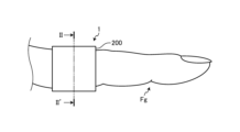
- FIG. 1 is a schematic diagram showing an example of the external appearance of a detection device according to an embodiment when a finger is placed inside the detection device as viewed from the side of a housing.
- FIG. 2 is a cross-sectional view taken along line II-II' of FIG.
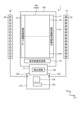
- FIG. 3 is a plan view illustrating the detection device according to the embodiment.
- FIG. 4 is a plan view showing a schematic example of the arrangement of the optical sensors and the solar cells in the detection area.
- FIG. 5 is a block diagram illustrating an example of the configuration of a detection device according to the embodiment.
- FIG. 6 is a circuit diagram showing a detection device according to an embodiment.
- FIG. 7 is a block diagram showing a schematic configuration example of the optical sensor, the solar cell, the battery circuit, and the light source.
- FIG. 1 is a schematic diagram showing an example of the external appearance of a detection device according to an embodiment when a finger is placed inside the detection device as viewed from the side of a housing.
- FIG. 2 is
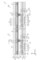
- FIG. 8 is a cross-sectional view taken along line VIII-VIII' of FIG.
- FIG. 9 is an enlarged cross-sectional view of the optical sensor in FIG.
- FIG. 10 is a cross-sectional view taken along line X-X' of FIG.
- FIG. 11 is an enlarged cross-sectional view of the solar cell in FIG.
- FIG. 12 is an explanatory diagram for explaining the relationship between the detection by the optical sensor of the detection device and the operation of the solar cell.
- FIG. 13 is a cross-sectional view of a detection device according to a modified example.
- FIG. 14 is an enlarged cross-sectional view of the solar cell in FIG.
- the term "on top” is used, unless otherwise specified, to include both a case in which another structure is placed directly on top of a structure so as to be in contact with the structure, and a case in which another structure is placed above a structure via yet another structure.
- FIG. 1 is a schematic diagram showing an example of the external appearance of a detection device according to an embodiment when a finger is placed inside the detection device as viewed from the side of a housing.
- Fig. 2 is a cross-sectional view taken along line II-II' of Fig. 1.
- the detection device 1 shown in Figs. 1 and 2 is a ring-shaped device that can be attached and detached to the human body, and is attached to a detectable object Fg of the human body.
- the detectable object Fg is a finger, and may be any of the thumb, index finger, middle finger, ring finger, little finger, etc.
- the detection device 1 can detect biometric information related to the living body from the detectable object Fg attached to it.
- the detection device 1 includes a housing 200, a light sensor PD (organic light sensor), a solar cell SC (organic photovoltaic element), a battery 73, and light sources 53, 54.
- the housing 200 houses the light sensor PD, the solar cell SC, the battery 73, and the light sources 53, 54 inside.
- components other than the housing 200, the light sensor PD, the solar cell SC, the battery 73, and the light sources 53, 54 are omitted.
- the housing 200 is formed in a ring shape (annular shape) that can be attached to the detectable object Fg, and is an attachment member that is attached to a living body.
- the housing 200 is formed of a housing material such as synthetic resin.
- the housing 200 has a first part 201 having an inner peripheral surface 201a that is translucent and an outer peripheral surface 201b that is non-translucent, and a second part 202 having an outer peripheral surface 202b that is translucent and an inner peripheral surface 202a that is non-translucent.
- the first part 201 faces the abdomen of the detectable object Fg
- the second part 202 is disposed on the opposite side of the abdomen of the detectable object Fg.
- the abdomen of the detectable object Fg is the inside of the detectable object Fg when the hand is closed.
- the parts of the housing 200 made of a non-translucent material are shown hatched, and the parts made of a translucent material are shown without hatching.
- the multiple optical sensors PD and the multiple solar cells SC are arranged along the shape of the annular housing 200. More specifically, the multiple optical sensors PD and the multiple solar cells SC are arranged in the first part 201 and the second part 202 of the annular housing 200, respectively.
- the multiple optical sensors PD provided in the first part 201 detect biological information related to a living organism from the detectable object Fg (see FIG. 1). Specifically, light emitted from the light sources 53, 54 and transmitted through or reflected by the detectable object Fg (see FIG. 1) is irradiated onto the multiple optical sensors PD through the translucent inner surface 201a of the first part 201. In addition, the non-translucent outer surface 201b of the first part 201 blocks natural light that enters the multiple optical sensors PD from the outside.
- the multiple solar cells SC provided in the second part 202 generate electricity using natural light irradiated from the outside.
- the natural light from the outside is irradiated to the multiple solar cells SC through the translucent outer surface 202b of the second part 202.
- the non-translucent inner surface 202a of the second part 202 can prevent the natural light from the outside from traveling as stray light toward the object to be detected Fg and the first part 201.
- the non-translucent inner surface 202a of the second part 202 blocks light emitted from the light sources 53, 54 and incident on the solar cells SC of the second part 202.
- the total area of the optical sensors PD is larger than the total area of the solar cells SC, and in the second portion 202, the total area of the optical sensors PD is smaller than the total area of the solar cells SC.
- the multiple optical sensors PD provided in the first portion 201 have higher detection sensitivity than the second portion 202, and can effectively detect the biological information of the subject Fg (see FIG. 1).
- the multiple solar cells SC provided in the second portion 202 have higher power generation efficiency than the first portion 201, and can effectively generate power based on natural light from the outside.
- the optical sensors PD may be disposed in the first portion 201, and the solar cells SC may be disposed in the second portion 202.
- the light sources 53, 54 are provided in positions inside the housing 200 that do not overlap with the multiple optical sensors PD and multiple solar cells SC. Note that the positions of the light sources 53, 54 shown in FIG. 2 are merely examples and can be changed as appropriate. In other words, the light sources 53, 54 may be positioned in any way as long as the light emitted from the light sources 53, 54 and transmitted through or reflected by the object to be detected Fg is appropriately irradiated onto the optical sensor PD.
- the battery 73 is a secondary battery that can be used by repeatedly charging and discharging.
- the battery 73 is, for example, a film-type lithium ion battery.
- the battery 73 is charged with power generated by the multiple solar cells SC.
- the battery 73 also supplies stored power to each part that requires power for detection by the multiple optical sensors PD.
- the battery 73 supplies power to the light sources 53, 54, for example.
- the battery 73 is disposed between the outer peripheral surface 201b of the first part 201 and the multiple optical sensors PD and multiple solar cells SC.
- the battery 73 may be disposed in any position that does not impede detection by the optical sensors PD and power generation by the solar cells SC, specifically, as long as it is disposed in a position that does not block light from the light sources 53, 54 and natural light from the outside.
- FIG. 3 is a plan view that shows a schematic diagram of a detection device according to an embodiment.
- FIG. 4 is a plan view that shows a schematic diagram of an example of the arrangement of the optical sensors and solar cells in the detection area.
- FIGS. 3 and 4 are plan views that show a schematic diagram of the sensor substrate 21 in a flat state before being housed in the housing 200.
- the detection device 1 has a sensor substrate 21 (substrate), a sensor unit 10, a gate line driving circuit 15, a signal line selection circuit 16, a solar cell driving circuit 17, a detection circuit 48, a control circuit 122, a power supply circuit 123, a first light source substrate 51, a second light source substrate 52, and light sources 53 and 54.
- a plurality of light sources 53 are provided on the first light source substrate 51.
- a plurality of light sources 54 are provided on the second light source substrate 52.
- the control board 121 is electrically connected to the sensor board 21 via the wiring board 71.
- the wiring board 71 and the control board 121 are, for example, flexible printed circuit boards.
- the wiring board 71 is provided with a detection circuit 48.
- the control board 121 is provided with a control circuit 122 and a power supply circuit 123.
- the control circuit 122 is, for example, an FPGA (Field Programmable Gate Array).
- the control circuit 122 supplies control signals to the sensor unit 10, the gate line driving circuit 15, the signal line selection circuit 16, and the solar cell driving circuit 17 to control the detection operation of the sensor unit 10.
- the control circuit 122 also supplies control signals to the light sources 53 and 54 to control the lighting or non-lighting of the light sources 53 and 54.
- the power supply circuit 123 supplies voltage signals such as a sensor power supply signal VDDSNS (see FIG. 6) to the sensor unit 10, the gate line driving circuit 15, the signal line selection circuit 16, and the solar cell driving circuit 17. In addition, the power supply circuit 123 supplies the power supply voltage to the light sources 53 and 54.
- VDDSNS sensor power supply signal
- the sensor substrate 21 has a detection area AA and a peripheral area GA.
- the detection area AA is an area in which the multiple optical sensors PD and multiple solar cells SC (see FIG. 4) of the sensor unit 10 are provided.
- the peripheral area GA is an area between the outer periphery of the detection area AA and the outer edge of the sensor substrate 21, and is an area in which the multiple optical sensors PD and multiple solar cells SC are not provided.
- the detection area AA has a first detection area AA1 and a second detection area AA2.
- the first detection area AA1 and the second detection area AA2 are arranged adjacent to each other in the second direction Dy.
- the first detection area AA1 is disposed in the first part 201 of the housing 200
- the second detection area AA2 is disposed in the second part 202 of the housing 200.
- the second direction Dy of the sensor board 21 is disposed along the circumferential direction of the housing 200.
- the first direction Dx is a direction in a plane parallel to the sensor substrate 21.
- the second direction Dy is a direction in a plane parallel to the sensor substrate 21, and is a direction perpendicular to the first direction Dx.
- the second direction Dy may intersect the first direction Dx without being perpendicular to it.
- the third direction Dz is a direction perpendicular to the first direction Dx and the second direction Dy, and is a normal direction to the main surface of the sensor substrate 21.
- plane view refers to the positional relationship when the sensor substrate 21 is unfolded in a planar shape and viewed from a direction perpendicular to the sensor substrate 21.
- the multiple sensor pixels PX and the multiple solar cell pixels PXA are arranged in a matrix in the detection area AA.
- the multiple sensor pixels PX include a photosensor PD.
- the multiple solar cell pixels PXA include a solar cell SC.
- the arrangement density (area) of the multiple sensor pixels PX and the arrangement density (area) of the multiple solar cell pixels PXA in the first detection area AA1 are different from the arrangement density (area) of the multiple sensor pixels PX and the arrangement density (area) of the multiple solar cell pixels PXA in the second detection area AA2.
- one reference unit in the first detection area AA1, one reference unit includes three sensor pixels PX (photo sensor PD) and one solar cell pixel PXA (solar cell SC). In the second detection area AA2, one reference unit includes one sensor pixel PX (photo sensor PD) and three solar cell pixels PXA (solar cell SC).
- the sensor board 21 when the sensor board 21 is housed in the housing 200, as described above, the total area of the photosensors PD in the first portion 201 is larger than the total area of the solar cells SC, and the total area of the photosensors PD in the second portion 202 is smaller than the total area of the solar cells SC.
- the gate line driving circuit 15, the signal line selection circuit 16, and the solar cell driving circuit 17 are provided in the peripheral area GA. Specifically, the gate line driving circuit 15 and the solar cell driving circuit 17 are provided in an area of the peripheral area GA that extends along the second direction Dy.
- the signal line selection circuit 16 is provided in an area of the peripheral area GA that extends along the first direction Dx, and is provided between the sensor unit 10 and the detection circuit 48.
- the multiple light sources 53 are provided on the first light source substrate 51 and are arranged along the second direction Dy.
- the multiple light sources 54 are provided on the second light source substrate 52 and are arranged along the second direction Dy.
- the first light source substrate 51 and the second light source substrate 52 are electrically connected to the control circuit 122 and the power supply circuit 123 via terminal portions 124 and 125, respectively, provided on the control board 121.
- the multiple light sources 53 and the multiple light sources 54 may be, for example, inorganic light-emitting diodes (LEDs) or organic light-emitting diodes (OLEDs).
- the multiple light sources 53 and the multiple light sources 54 each emit light of a different wavelength.
- the first light emitted from the light source 53 is mainly reflected by the surface of the object to be detected, such as a finger, and enters the sensor unit 10. This allows the sensor unit 10 to detect a fingerprint by detecting the uneven shape of the surface of the finger.
- the second light emitted from the light source 54 is mainly reflected inside the finger or passes through the finger and enters the sensor unit 10. This allows the sensor unit 10 to detect information about a living body inside the finger.
- Information about a living body includes, for example, the pulse waves, pulse, and blood vessel images of the finger or palm.
- the detection device 1 may be configured as a fingerprint detection device that detects fingerprints, or a vein detection device that detects blood vessel patterns such as veins.
- the detection device 1 is provided with multiple types of light sources 53, 54 as light sources. However, this is not limited to this, and there may be only one type of light source. For example, multiple light sources 53 and multiple light sources 54 may be arranged on each of the first light source substrate 51 and the second light source substrate 52. Furthermore, there may be one light source substrate on which the light sources 53 and the light sources 54 are arranged, or there may be three or more light source substrates. Alternatively, it is sufficient that at least one light source is arranged.
- FIG. 5 is a block diagram showing an example of the configuration of a detection device according to an embodiment.
- the detection device 1 further includes a detection control circuit 11 and a detection unit 40. Some or all of the functions of the detection control circuit 11 are included in the control circuit 122. In addition, some or all of the functions of the detection unit 40 other than the detection circuit 48 are included in the control circuit 122.
- the sensor unit 10 has multiple optical sensors PD.
- the optical sensors PD of the sensor unit 10 output an electrical signal corresponding to the irradiated light as a detection signal Vdet to the signal line selection circuit 16.
- the sensor unit 10 also performs detection according to the gate drive signal VGL supplied from the gate line drive circuit 15.
- the detection control circuit 11 is a circuit that supplies control signals to the gate line drive circuit 15, the signal line selection circuit 16, and the detection unit 40, respectively, and controls their operation.
- the detection control circuit 11 supplies various control signals, such as a start signal STV and a clock signal CK, to the gate line drive circuit 15.
- the detection control circuit 11 also supplies various control signals, such as a selection signal ASW, to the signal line selection circuit 16.
- the detection control circuit 11 also supplies various control signals to the light sources 53 and 54, controlling their lighting and non-lighting.
- the gate line driving circuit 15 is a circuit that drives multiple gate lines GL (see FIG. 6) based on various control signals.
- the gate line driving circuit 15 selects multiple gate lines GL sequentially or simultaneously, and supplies a gate driving signal VGL to the selected gate lines GL. In this way, the gate line driving circuit 15 selects multiple photosensors PD connected to the gate lines GL.
- the signal line selection circuit 16 is a switch circuit that sequentially or simultaneously selects multiple signal lines SL (see FIG. 6).
- the signal line selection circuit 16 is, for example, a multiplexer.
- the signal line selection circuit 16 connects the selected signal line SL to the detection circuit 48 based on the selection signal ASW supplied from the detection control circuit 11. As a result, the signal line selection circuit 16 outputs the detection signal Vdet of the optical sensor PD to the detection unit 40.
- the detection unit 40 includes a detection circuit 48, a signal processing circuit 44, a coordinate extraction circuit 45, a memory circuit 46, and a detection timing control circuit 47.
- the detection timing control circuit 47 controls the detection circuit 48, the signal processing circuit 44, and the coordinate extraction circuit 45 to operate in synchronization based on a control signal supplied from the detection control circuit 11.
- the detection circuit 48 is, for example, an analog front-end circuit (AFE).
- the detection circuit 48 is a signal processing circuit having at least the functions of a detection signal amplifier circuit 42 and an A/D conversion circuit 43.
- the detection signal amplifier circuit 42 amplifies the detection signal Vdet.
- the A/D conversion circuit 43 converts the analog signal output from the detection signal amplifier circuit 42 into a digital signal.
- the signal processing circuit 44 is a logic circuit that detects a predetermined physical quantity input to the sensor unit 10 based on the output signal of the detection circuit 48. When a finger touches or approaches the detection surface, the signal processing circuit 44 can detect unevenness on the surface of the finger or palm based on the signal from the detection circuit 48. The signal processing circuit 44 can also detect information about the living body based on the signal from the detection circuit 48. Information about the living body includes, for example, blood vessel images of the finger or palm, pulse waves, pulse rate, blood oxygen concentration, etc.
- the memory circuit 46 temporarily stores the signal calculated by the signal processing circuit 44.
- the memory circuit 46 may be, for example, a RAM (Random Access Memory), a register circuit, etc.
- the coordinate extraction circuit 45 is a logic circuit that determines the detection coordinates of the unevenness of the surface of a finger, etc., when the signal processing circuit 44 detects contact or proximity of a finger.
- the coordinate extraction circuit 45 is also a logic circuit that determines the detection coordinates of the blood vessels of the finger or palm.
- the coordinate extraction circuit 45 combines the detection signals Vdet output from each optical sensor PD of the sensor unit 10 to generate two-dimensional information indicating the shape of the unevenness of the surface of the finger, etc., and two-dimensional information indicating the shape of the blood vessels of the finger or palm.
- the coordinate extraction circuit 45 may output the detection signal Vdet as the sensor output voltage Vo without calculating the detection coordinates.
- FIG. 6 is a circuit diagram showing a detection device according to an embodiment. Note that FIG. 6 also shows the circuit configuration of detection circuit 48. Furthermore, FIG. 6 omits the solar cell SC and shows only the sensor pixel PX and detection circuit 48. As shown in FIG. 7, the solar cell SC is charged to a battery 73 via a charge control circuit 72 through a separate route. As shown in FIG. 6, the sensor pixel PX includes a photosensor PD, a capacitance element Ca, and a drive transistor Tr.
- the capacitance element Ca is a capacitance (sensor capacitance) formed in the photosensor PD, and is equivalently connected in parallel with the photosensor PD.
- FIG. 6 of the multiple gate lines GL two gate lines GL(m) and GL(m+1) aligned in the second direction Dy are shown. Also, of the multiple signal lines SL, two signal lines SL(n) and SL(n+1) aligned in the first direction Dx are shown.
- the sensor pixel PX is the area surrounded by the gate line GL and the signal line SL.
- the multiple gate lines GL each extend in a first direction Dx and are arranged at intervals in the second direction Dy.
- the multiple signal lines SL each extend in the second direction Dy and are arranged at intervals in the first direction Dx.
- the multiple sensor pixels PX (multiple photosensors PD) are provided in an area surrounded by two gate lines GL and two signal lines SL.
- the drive transistor Tr is provided corresponding to each of the multiple photosensors PD.
- the drive transistor Tr is composed of a thin film transistor, and in this example, is composed of an n-channel MOS (Metal Oxide Semiconductor) type TFT (Thin Film Transistor).
- Each of the multiple gate lines GL is connected to the gates of multiple drive transistors Tr arranged in a first direction Dx.
- Each of the multiple signal lines SL is connected to one of the sources and drains of multiple drive transistors Tr arranged in a second direction Dy.
- the other of the sources and drains of the multiple drive transistors Tr is connected to the anode of the photosensor PD and the capacitive element Ca.
- the cathode of the optical sensor PD is supplied with a sensor power supply signal VDDSNS from the power supply circuit 123 (see FIG. 1).
- the signal line SL and the capacitance element Ca are supplied with a sensor reference voltage COM, which is the initial potential of the signal line SL and the capacitance element Ca, from the power supply circuit 123 via the reset transistor TrR.
- the switch SSW of the detection circuit 48 is turned on and connected to the signal line SL.
- the detection signal amplifier circuit 42 of the detection circuit 48 converts the fluctuation in the current supplied from the signal line SL into a fluctuation in voltage and amplifies it.
- a reference potential (Vref) having a fixed potential is input to the non-inverting input section (+) of the detection signal amplifier circuit 42, and the signal line SL is connected to the inverting input section (-).
- a signal equal to the sensor reference voltage COM is input as the reference potential (Vref) voltage.
- the control circuit 122 see FIG.
- the detection signal amplifier circuit 42 also has a capacitance element Cb and a reset switch RSW. During the reset period, the reset switch RSW is turned on and the charge of the capacitance element Cb is reset.
- the driving transistor Tr is not limited to an n-type TFT, and may be a p-type TFT.
- the pixel circuit of the sensor pixel PX shown in FIG. 6 is merely an example, and the sensor pixel PX may be provided with multiple transistors corresponding to one photosensor PD.
- FIG. 7 is a block diagram showing a schematic example of the configuration of the light sensor, solar cell, battery circuit, and light source.
- the detection device 1 has a detection circuit 48 connected to the light sensor PD, and a battery circuit 74 connected to the solar cell SC.
- the detection circuit 48 has been explained in FIGS. 5 and 6, so a repeated explanation will be omitted.
- the battery circuit 74 includes a charge control circuit 72 and a battery 73.
- the charge control circuit 72 is a circuit that adjusts the power supplied from the solar cell SC to control the charging of the battery 73.
- the charge control circuit 72 is connected between the connection transistor TrA (see FIG. 8) and the solar cell SC to adjust the power charged to the battery 73.
- the charge control circuit 72 controls the operation of the solar cell drive circuit 17 (see FIG. 3) to control the operation of the connection transistor TrA and adjusts the power supplied from the solar cell SC to the battery 73.
- the connection transistor TrA and the battery 73 may be directly connected.
- the charge control circuit 72 appropriately adjusts the voltage value and current value output to the battery 73 according to the state (capacity, temperature, etc.) of the battery 73. Also, when the light sensor PD and the detection circuit 48 are performing a detection operation, the connection transistor TrA may be turned off to stop charging the battery 73, and when the detection operation is not performed, the connection transistor TrA may be turned on to charge the battery 73.
- the battery 73 supplies a drive voltage VLED to the light sources 53 and 54.
- the light sources 53 and 54 emit light L1 using the drive voltage VLED.
- the optical sensor PD outputs an electrical signal corresponding to the irradiated light L1 as a detection signal Vdet.
- the detection circuit 48 processes the detection signal Vdet from the optical sensor PD as described above.
- the battery 73 supplies the driving voltage VLED to the light sources 53 and 54, but it may also be used to power other components and circuits of the detection device 1 as needed.
- Figure 8 is a cross-sectional view taken along line VIII-VIII' in Figure 4.
- the direction perpendicular to the surface of the sensor substrate 21, from the sensor substrate 21 toward the sealing film 90 is referred to as the "upper side” or simply “top”.
- the direction from the sealing film 90 toward the sensor substrate 21 is referred to as the “lower side” or simply “bottom”.
- the detection device 1 is formed by stacking a TFT layer, an organic insulating film 27, an inorganic insulating film 28, a photosensor PD and a solar cell SC, and a sealing film 90 on a sensor substrate 21 in this order.
- the TFT layer is a circuit formation layer in which the drive transistor Tr, the connection transistor TrA, and various wiring such as the gate line GL and the signal line SL are provided.
- the sensor substrate 21 is an insulating substrate formed from a film-like resin.
- the drive transistor Tr provided in the TFT layer is provided in a region that overlaps with the first lower electrode 23 of the photosensor PD.
- the drive transistor Tr has a semiconductor layer 61, a source electrode 62, a drain electrode 63, and a gate electrode 64.
- connection transistor TrA is provided in a region that overlaps with the second lower electrode 25 of the solar cell SC.
- the connection transistor TrA has a semiconductor layer 61A, a source electrode 62A, a drain electrode 63A, and a gate electrode 64A.
- the TFT layer has insulating films, which are an undercoat film 91, a gate insulating film 92, an interlayer insulating film 93, and an overlapping insulating film 94.
- the light-shielding film 65 is provided on the sensor substrate 21.
- the light-shielding film 65 is provided between the semiconductor layer 61 and the sensor substrate 21.
- the light-shielding film 65 can prevent light from entering the channel region of the semiconductor layer 61 from the sensor substrate 21 side.
- the undercoat film 91 is provided on the sensor substrate 21, covering the light-shielding film 65.
- the undercoat film 91 is formed of an inorganic insulating film, such as a silicon nitride film or a silicon oxide film.
- the configuration of the undercoat film 91 is not limited to that shown in FIG. 8.
- the undercoat film 91 may be a laminated film having two or more layers stacked on top of each other.
- the drive transistor Tr is provided on the sensor substrate 21.
- the semiconductor layer 61 is provided on the undercoat film 91.
- the gate insulating film 92 is provided on the undercoat film 91, covering the semiconductor layer 61.
- the gate insulating film 92 is an inorganic insulating film, such as a silicon oxide film.
- the gate electrode 64 is provided on the gate insulating film 92.
- the driving transistor Tr has a top gate structure. However, this is not limited to this, and the driving transistor Tr may have a bottom gate structure, or a dual gate structure in which a gate electrode 64 is provided on both the upper and lower sides of the semiconductor layer 61.
- connection wiring 64a is provided in the same layer as the gate electrode 64.
- the connection wiring 64a is electrically connected to the gate electrode 64.
- a connection wiring 65a is provided in the same layer as the light-shielding film 65.
- the connection wiring 65a is electrically connected to the light-shielding film 65.
- the connection wiring 64a and the connection wiring 65a are connected via a contact hole CH4 that penetrates the undercoat film 91 and the gate insulating film 92.
- the light-shielding film 65 is electrically connected to the gate electrode 64 via the connection wirings 64a and 65a, and is supplied with the same potential as the gate electrode 64.
- connection transistor TrA the configurations of the light-shielding film 65A and the connection wirings 64Aa and 65Aa provided in the connection transistor TrA are similar to those of the light-shielding film 65 and the connection wirings 64a and 65a provided in the drive transistor Tr.
- the interlayer insulating film 93 is provided on the gate insulating film 92, covering the gate electrode 64.
- the interlayer insulating film 93 has, for example, a laminated structure of a silicon nitride film and a silicon oxide film.
- the source electrode 62 and the drain electrode 63 are provided on the interlayer insulating film 93.
- the source electrode 62 is connected to the source region of the semiconductor layer 61 through a contact hole CH2 provided in the gate insulating film 92 and the interlayer insulating film 93.
- the drain electrode 63 is connected to the drain region of the semiconductor layer 61 through a contact hole CH3 provided in the gate insulating film 92 and the interlayer insulating film 93.
- the overlapping insulating film 94 is provided on the interlayer insulating film 93, covering the source electrode 62 and the drain electrode 63.
- the organic insulating film 27 is provided on the overlapping insulating film 94, covering the source electrode 62 and drain electrode 63 of the drive transistor Tr.
- the organic insulating film 27 is a planarizing film formed of an organic insulating material.
- the contact hole CH1 in the organic insulating film 27 is provided in a region overlapping with the source electrode 62.
- the first lower electrode 23 of the photosensor PD is electrically connected to the source electrode 62 at the bottom of the contact hole CH1.
- the inorganic insulating film 28 is provided on the organic insulating film 27.
- the inorganic insulating film 28 is a barrier film formed from an inorganic insulating material such as silicon nitride (SiN).
- FIG. 9 is an enlarged cross-sectional view of the photosensor in Figure 8. Note that in Figure 8, the first lower buffer layer 32 and the first upper buffer layer 33 of the photosensor PD are omitted.
- the photosensor PD has a first lower electrode 23, a first lower buffer layer 32, a first active layer 31, a first upper buffer layer 33, a first upper electrode 24, and a common electrode 29.
- the photosensor PD is stacked in the order of the first lower electrode 23, the first lower buffer layer 32 (hole transport layer), the first active layer 31, the first upper buffer layer 33 (electron transport layer), the first upper electrode 24, and the common electrode 29 in a direction perpendicular to the sensor substrate 21.
- the photosensor PD of this embodiment is a photodiode (OPD: Organic Photodiode) in which an organic semiconductor is used as the first active layer 31.
- OPD Organic Photodiode
- the first lower electrode 23 is an anode electrode of the photosensor PD, and is formed of a conductive material having translucency, such as ITO (Indium Tin Oxide).
- the first lower electrode 23 is provided separately for each photosensor PD.
- the first lower buffer layer 32, the first active layer 31, the first upper buffer layer 33, and the first upper electrode 24 are provided continuously across multiple photosensors PD. Specifically, the first lower buffer layer 32, the first active layer 31, the first upper buffer layer 33, and the first upper electrode 24 are provided overlapping multiple first lower electrodes 23 of adjacent photosensors PD, and also overlapping the insulating film 35 between adjacent photosensors PD.
- the insulating film 35 is provided to cover the periphery of the first lower electrode 23. Although not shown, the insulating film 35 is provided on the inorganic insulating film 28 between the first lower electrodes 23 of the adjacent photosensors PD. The insulating film 35 insulates the first lower electrodes 23 of the adjacent photosensors PD. The insulating film 35 is also provided to cover the contact hole CH1, and covers the first lower electrode 23 in the area overlapping with the contact hole CH1. As a result, even if a step occurs in the first lower buffer layer 32 (hole transport layer) inside the contact hole CH1, the insulating film 35 can suppress the occurrence of a short circuit between the first active layer 31 and the first lower electrode 23. In this embodiment, the insulating film 35 is formed of an inorganic insulating material such as a silicon nitride film (SiN) or a silicon oxide film (SiO 2 ).
- SiN silicon nitride film
- SiO 2 silicon oxide film
- the contact hole CH1 is provided at the center of the first lower electrode 23, penetrating the organic insulating film 27 in the thickness direction (third direction Dz).
- the first lower electrode 23 is connected to the source electrode 62 at the bottom of the contact hole CH1.
- the position of the contact hole CH1, i.e., the connection point between the photosensor PD and the drive transistor Tr, is not limited to the center of the first lower electrode 23, and can be changed as appropriate.
- the characteristics (for example, voltage-current characteristics and resistance value) of the first active layer 31 change depending on the light irradiated.
- An organic material is used as the material of the first active layer 31.
- the first active layer 31 is a bulk heterostructure in which a p-type organic semiconductor and an n-type fullerene derivative (PCBM), which is an n-type organic semiconductor, are mixed.
- PCBM n-type fullerene derivative
- low molecular weight organic materials such as C60 (fullerene), PCBM (phenyl C61-butyric acid methyl ester), CuPc (copper phthalocyanine), F16CuPc (fluorinated copper phthalocyanine), rubrene (5,6,11,12-tetraphenyltetracene), and PDI (perylene derivative) can be used as the first active layer 31.
- C60 fulllerene
- PCBM phenyl C61-butyric acid methyl ester
- CuPc copper phthalocyanine
- F16CuPc fluorinated copper phthalocyanine
- rubrene 5,6,11,12-tetraphenyltetracene
- PDI perylene derivative
- the first active layer 31 can be formed by a deposition type (dry process) using these low molecular weight organic materials.
- the first active layer 31 may be, for example, a laminated film of CuPc and F16CuPc, or a laminated film of rubrene and C60.
- the first active layer 31 can also be formed by a coating type (wet process).
- the first active layer 31 is made of a material that combines the above-mentioned low molecular weight organic material and a polymer organic material.
- the polymer organic material for example, P3HT (poly(3-hexylthiophene)), F8BT (F8-alt-benzothiadiazole), etc. can be used.
- the first active layer 31 can be a film in a state where P3HT and PCBM are mixed, or a film in a state where F8BT and PDI are mixed.
- the first lower buffer layer 32 is a hole transport layer
- the first upper buffer layer 33 is an electron transport layer.
- the first lower buffer layer 32 and the first upper buffer layer 33 are provided to facilitate the holes and electrons generated in the first active layer 31 to reach the first lower electrode 23 or the first upper electrode 24.
- the first lower buffer layer 32 (hole transport layer) is in direct contact with the top of the first lower electrode 23, and is also provided on the insulating film 35 between the adjacent first lower electrodes 23.
- the first active layer 31 is in direct contact with the top of the first lower buffer layer 32.
- the material of the hole transport layer is a metal oxide layer. Tungsten oxide (WO 3 ), molybdenum oxide, or the like is used as the metal oxide layer.
- the first upper buffer layer 33 (electron transport layer) is in direct contact with the first active layer 31, and the first upper electrode 24 is in direct contact with the first upper buffer layer 33.
- the material used for the electron transport layer is ethoxylated polyethyleneimine (PEIE).
- the materials and manufacturing methods of the first lower buffer layer 32, the first active layer 31, and the first upper buffer layer 33 are merely examples, and other materials and manufacturing methods may be used.
- the first lower buffer layer 32 and the first upper buffer layer 33 are not limited to single-layer films, and may be formed as a laminated film including an electron blocking layer and a hole blocking layer.
- the first upper electrode 24 is provided on the first upper buffer layer 33.
- the first upper electrode 24 is a cathode electrode of the optical sensor PD, and is formed continuously over the entire detection area AA. In other words, the first upper electrode 24 is provided continuously over the multiple optical sensors PD.
- the first upper electrode 24 faces the multiple first lower electrodes 23, sandwiching the first lower buffer layer 32, the first active layer 31, and the first upper buffer layer 33 therebetween.
- the first upper electrode 24 is formed of a non-transparent conductive material, such as silver (Ag).
- the common electrode 29 is provided on the first upper electrode 24.
- the common electrode 29 is provided continuously across the multiple photosensors PD and the multiple solar cells SC.
- the common electrode 29 is formed of a translucent conductive material such as ITO.
- a common reference potential is supplied to the multiple photosensors PD and the multiple solar cells SC via the common electrode 29.
- FIG. 10 is a cross-sectional view taken along the line X-X' in FIG. 4.
- a common electrode connection terminal 81 is provided in the peripheral area GA of the sensor substrate 21.
- the common electrode 29 is provided continuously from the detection area AA to the peripheral area GA, and is connected to the common electrode connection terminal 81 in the peripheral area GA.
- the common electrode connection terminal 81 is provided on the overlapping insulating film 94 in the peripheral area GA. Furthermore, reference potential supply wiring 82, 83 is provided between the common electrode connection terminal 81 and the sensor substrate 21. The common electrode connection terminal 81 is connected to the reference potential supply wiring 82, and a reference potential is supplied to the common electrode connection terminal 81.
- the organic insulating film 27 and inorganic insulating film 28 are removed, and the insulating film 35, first active layer 31, common electrode 29, and sealing film 90 are stacked in this order on the superimposed insulating film 94.
- the insulating film 35 and first active layer 31 are not provided, and the common electrode 29 and sealing film 90 are stacked in this order on the common electrode connection terminal 81.
- the sealing film 90 is provided on the common electrode 29 and is provided continuously to cover the multiple photosensors PD and multiple solar cells SC.
- the sealing film 90 is made of an inorganic film such as a silicon nitride film or an aluminum oxide film, or a resin film such as acrylic.
- the sealing film 90 is not limited to a single layer, but may be a laminated film of two or more layers combining the above-mentioned inorganic films and resin films.
- the sealing film 90 provides a good seal for the multiple photosensors PD and multiple solar cells SC, and can prevent moisture from entering from the upper surface side.
- FIG. 11 is an enlarged cross-sectional view of the solar cell in Figure 8. Note that in Figure 8, the second lower buffer layer 37 and the second upper buffer layer 38 of the solar cell SC are omitted.
- the solar cell SC has a structure similar to that of the photosensor PD and is a photodiode (OPD) in which an organic semiconductor is used as the second active layer 36.
- the solar cell SC has a second lower electrode 25, a second lower buffer layer 37, a second active layer 36, a second upper buffer layer 38, and a common electrode 29.
- the solar cell SC is stacked in the order of the second lower electrode 25, the second lower buffer layer 37 (hole transport layer), the second active layer 36, the second upper buffer layer 38 (electron transport layer), and the common electrode 29 in the direction perpendicular to the sensor substrate 21.
- the second lower electrode 25, second lower buffer layer 37 (hole transport layer), second active layer 36, and second upper buffer layer 38 of the solar cell SC are provided in the same layer as the first lower electrode 23, first lower buffer layer 32, first active layer 31, and first upper buffer layer 33 of the photosensor PD, respectively.
- first lower electrode 23, first lower buffer layer 32, first active layer 31, first upper buffer layer 33, and first upper electrode 24 of the photosensor PD are provided at a distance from the second lower electrode 25, second lower buffer layer 37, second active layer 36, and second upper buffer layer 38 of the solar cell SC.
- a common electrode 29 and a sealing film 90 are provided between adjacent photosensors PD and solar cells SC.
- the common electrode 29 is provided to cover the side surface of the first active layer 31 of the photosensor PD, the side surface of the first upper electrode 24, and the side surface of the second active layer 36 of the solar cell SC.
- the sealing film 90 is provided to cover the common electrode 29 formed in a concave shape between the adjacent photosensors PD and solar cells SC.
- the second lower electrode 25 of the solar cell SC is formed of a non-translucent conductive material such as silver (Ag).
- the second lower electrode 25 is provided separately for each solar cell SC.
- the insulating film 35 is provided to cover the peripheral portion of the second lower electrode 25.
- the insulating film 35 is provided on the inorganic insulating film 28 between the adjacent first lower electrode 23 and second lower electrode 25.
- the insulating film 35 insulates the first lower electrode 23 of the adjacent photosensor PD from the second lower electrode 25 of the solar cell SC.
- the insulating film 35 is also provided to cover the contact hole CH5, and covers the second lower electrode 25 in the area overlapping with the contact hole CH5.
- the second lower buffer layer 37, the second active layer 36, and the second upper buffer layer 38 of the solar cell SC are formed from the same materials as the first lower buffer layer 32, the first active layer 31, and the first upper buffer layer 33 of the photosensor PD, respectively.
- the common electrode 29 is provided on the second upper buffer layer 38. In other words, the common electrode 29 also serves as the upper electrode of the solar cell SC.
- the first lower electrode 23 of the optical sensor PD is translucent, and the first upper electrode 24 is non-translucent.
- the optical sensor PD is configured as a bottom-receiving type.
- Light L1 emitted from the light sources 53, 54 and transmitted through or reflected by the object to be detected Fg is irradiated onto the first lower electrode 23 side of the optical sensor PD.
- the light L1 passes through the sensor substrate 21 and the first lower electrode 23 of the optical sensor PD, and is irradiated onto the first active layer 31.
- the second lower electrode 25 of the solar cell SC is non-transparent, and the common electrode 29 is translucent.
- the solar cell SC is configured as a top-side light-receiving type. Natural light L2 from the outside is irradiated onto the common electrode 29 side of the solar cell SC. Specifically, the natural light L2 passes through the sealing film 90 and the common electrode 29 of the solar cell SC and is irradiated onto the second active layer 36.
- the light sensor PD is irradiated with light L1 that has passed through or been reflected by the object to be detected Fg, and natural light L2 is blocked by the first upper electrode 24.
- the solar cell SC is irradiated with natural light L2, and light L1 that has passed through or been reflected by the object to be detected Fg is blocked by the second lower electrode 25. Therefore, the detection device 1 can effectively detect light and generate electricity by the light sensor PD and solar cell SC that are provided on the same sensor substrate 21.
- the optical sensor PD and solar cell SC shown in FIG. 8 are housed in the housing 200 shown in FIG. 2 to form the detection device 1.
- the lower surface of the sensor substrate 21 faces the inner surfaces 201a and 202a of the housing 200
- the common electrode 29 and sealing film 90 face the outer surfaces 201b and 202b of the housing 200.
- the optical sensor PD and solar cell SC mounted on the same sensor board 21 are housed in the annular housing 200, the optical sensor PD is irradiated with light L1 transmitted through or reflected by the object to be detected Fg from the inner circumferential surfaces 201a, 202a, and the solar cell SC is irradiated with natural light L2 from the outer circumferential surfaces 201b, 202b. Therefore, even when the optical sensor PD and solar cell SC are housed in the annular housing 200, the detection device 1 can detect light and generate electricity well.
- the outer peripheral surface 201b and inner peripheral surface 202a of the housing 200 are non-translucent. Therefore, in the optical sensor PD arranged in the first portion 201, natural light L2 is blocked by the first upper electrode 24 and the outer peripheral surface 201b of the housing 200. Furthermore, in the solar cell SC arranged in the second portion 202, light L1 is blocked by the second lower electrode 25 and the inner peripheral surface 202a of the housing 200. This improves the detection sensitivity of the optical sensor PD.
- the first lower electrode 23 needs to be translucent, and in the solar cell SC, at least the common electrode 29 needs to be translucent. That is, the first upper electrode 24 of the light sensor PD and the second lower electrode 25 of the solar cell SC may also be formed of a translucent conductive material such as ITO. Even in this case, the light sensor PD and the solar cell SC are housed in the housing 200 as described above, thereby ensuring the detection sensitivity of the light sensor PD and the power generation efficiency of the solar cell SC.
- FIG. 12 is an explanatory diagram for explaining the relationship between the detection of the optical sensor of the detection device and the operation of the solar cell.
- the detection device 1 performs a detection period T in which the optical sensor PD performs detection, and a charging period TA in which the solar cell SC charges the battery 73, in a time-division manner.
- the detection period T and the charging period TA are arranged alternately, such as detection period T, charging period TA, detection period T, charging period TA.
- the detection device 1 executes a reset period Prst, an effective exposure period Pex, and a readout period Pdet.
- the gate line driving circuit 15 sequentially scans the gate lines GL(1) to GL(M). That is, during the detection period T, the photosensors PD in the entire detection area AA are scanned.
- the light sources 53 and 54 are turned on and emit light L1. Also, during the detection period T, the operation of the battery circuit 74 is stopped and charging of the battery 73 is stopped.
- the solar cell drive circuit 17 turns on the connection transistor TrA (conducting state), and the current generated in the solar cell SC in response to the irradiated natural light L2 is supplied to the battery circuit 74.
- the charge control circuit 72 charges the battery 73.
- the gate line driving circuit 15 stops and the light sources 53 and 54 are not lit. In other words, during the charging period TA, no detection is performed by the light sensor PD.
- the detection device 1 can improve the detection sensitivity of the optical sensor PD by performing the detection period T and the charging period TA in a time-division manner, and can efficiently charge the battery 73 using the solar cell SC.
- the operation example shown in FIG. 12 is merely one example, and the detection by the optical sensor PD and the charging of the battery 73 by the solar cell SC can also be performed during the same period. Also, the detection period T and the charging period TA are arranged alternately, but the period (length) of the detection period T and the charging period TA can be appropriately changed depending on the power generation state of the solar cell SC and the capacity of the battery 73.
- FIG. 13 is a cross-sectional view of a detection device according to a modified example.
- Fig. 14 is an enlarged cross-sectional view of the solar cell in Fig. 13.
- the same components as those described in the above embodiment are designated by the same reference numerals, and duplicated description will be omitted.
- the solar cell SC has a second upper electrode 26. More specifically, the solar cell SC has a second lower electrode 25, a second lower buffer layer 37, a second active layer 36, a second upper buffer layer 38, a second upper electrode 26, and a common electrode 29 stacked in this order on the sensor substrate 21.
- the laminated structure of the optical sensor PD is the same as that shown in FIG. 9 described above, and a repeated explanation will be omitted.
- the first upper electrode 24 and the common electrode 29 of the optical sensor PD are translucent, and the first lower electrode 23 is non-translucent.
- the optical sensor PD is configured as a top-side light-receiving type.
- Light L1 emitted from the light sources 53, 54 and transmitted through or reflected by the object to be detected Fg is irradiated onto the first upper electrode 24 side of the optical sensor PD.
- the light L1 passes through the sealing film 90 and the common electrode 29 and first upper electrode 24 of the optical sensor PD, and is irradiated onto the first active layer 31.
- the second lower electrode 25 of the solar cell SC is translucent, and the second upper electrode 26 is non-translucent. That is, the solar cell SC is configured as a bottom-side light-receiving type. Natural light L2 from the outside is irradiated onto the second lower electrode 25 side of the solar cell SC. That is, natural light L2 passes through the sensor substrate 21 and the second lower electrode 25 of the solar cell SC and is irradiated onto the second active layer 36.
- the light sensor PD is irradiated with light L1 that has passed through or been reflected by the object to be detected Fg, and natural light L2 is blocked by the first lower electrode 23.
- the solar cell SC is irradiated with natural light L2, and the light L1 that has passed through or been reflected by the object to be detected Fg is blocked by the second upper electrode 26. Therefore, the detection device 1A according to the modified example can effectively detect light and generate electricity by the light sensor PD and solar cell SC that are provided on the same sensor substrate 21.
- the bottom surface of the sensor substrate 21 faces the outer peripheral surfaces 201b and 202b of the housing 200, and the common electrode 29 and sealing film 90 face the inner peripheral surfaces 201a and 202a of the housing 200.
Landscapes
- Engineering & Computer Science (AREA)
- Health & Medical Sciences (AREA)
- Physics & Mathematics (AREA)
- Computer Hardware Design (AREA)
- Theoretical Computer Science (AREA)
- Life Sciences & Earth Sciences (AREA)
- Human Computer Interaction (AREA)
- General Engineering & Computer Science (AREA)
- General Physics & Mathematics (AREA)
- Biomedical Technology (AREA)
- Veterinary Medicine (AREA)
- Public Health (AREA)
- Biophysics (AREA)
- Pathology (AREA)
- General Health & Medical Sciences (AREA)
- Heart & Thoracic Surgery (AREA)
- Medical Informatics (AREA)
- Molecular Biology (AREA)
- Surgery (AREA)
- Animal Behavior & Ethology (AREA)
- Power Engineering (AREA)
- Spectroscopy & Molecular Physics (AREA)
- Optics & Photonics (AREA)
- Dentistry (AREA)
- Oral & Maxillofacial Surgery (AREA)
- Cardiology (AREA)
- Physiology (AREA)
- Light Receiving Elements (AREA)
- Image Input (AREA)
Priority Applications (2)
| Application Number | Priority Date | Filing Date | Title |
|---|---|---|---|
| JP2025505189A JPWO2024185478A1 (https=) | 2023-03-03 | 2024-02-20 | |
| US19/313,450 US20250386659A1 (en) | 2023-03-03 | 2025-08-28 | Detection device |
Applications Claiming Priority (2)
| Application Number | Priority Date | Filing Date | Title |
|---|---|---|---|
| JP2023032743 | 2023-03-03 | ||
| JP2023-032743 | 2023-03-03 |
Related Child Applications (1)
| Application Number | Title | Priority Date | Filing Date |
|---|---|---|---|
| US19/313,450 Continuation US20250386659A1 (en) | 2023-03-03 | 2025-08-28 | Detection device |
Publications (1)
| Publication Number | Publication Date |
|---|---|
| WO2024185478A1 true WO2024185478A1 (ja) | 2024-09-12 |
Family
ID=92674647
Family Applications (1)
| Application Number | Title | Priority Date | Filing Date |
|---|---|---|---|
| PCT/JP2024/005911 Ceased WO2024185478A1 (ja) | 2023-03-03 | 2024-02-20 | 検出装置 |
Country Status (3)
| Country | Link |
|---|---|
| US (1) | US20250386659A1 (https=) |
| JP (1) | JPWO2024185478A1 (https=) |
| WO (1) | WO2024185478A1 (https=) |
Citations (7)
| Publication number | Priority date | Publication date | Assignee | Title |
|---|---|---|---|---|
| JP2010263190A (ja) * | 2009-03-24 | 2010-11-18 | Rohm Co Ltd | 半導体装置、光電変換装置および光電変換装置の製造方法 |
| JP2014053310A (ja) * | 2012-09-10 | 2014-03-20 | Samsung Electronics Co Ltd | 透光性電極とこれを備える有機光電素子及び有機発光ダイオード並びにイメージセンサー |
| WO2016002610A1 (ja) * | 2014-06-30 | 2016-01-07 | シャープ株式会社 | 撮像パネル及び当該撮像パネルを備えるx線撮像システム |
| US9407845B1 (en) * | 2015-03-26 | 2016-08-02 | Amazon Technologies, Inc. | Self powering camera |
| JP2017506376A (ja) * | 2013-11-29 | 2017-03-02 | モティヴ・インコーポレーテッドMotiv Inc. | ウェアラブルコンピューティングデバイス |
| JP2019513035A (ja) * | 2016-03-18 | 2019-05-23 | クアルコム,インコーポレイテッド | 心臓血管診断のための光学測定デバイス |
| WO2022220287A1 (ja) * | 2021-04-14 | 2022-10-20 | 株式会社ジャパンディスプレイ | 検出装置 |
-
2024
- 2024-02-20 JP JP2025505189A patent/JPWO2024185478A1/ja active Pending
- 2024-02-20 WO PCT/JP2024/005911 patent/WO2024185478A1/ja not_active Ceased
-
2025
- 2025-08-28 US US19/313,450 patent/US20250386659A1/en active Pending
Patent Citations (7)
| Publication number | Priority date | Publication date | Assignee | Title |
|---|---|---|---|---|
| JP2010263190A (ja) * | 2009-03-24 | 2010-11-18 | Rohm Co Ltd | 半導体装置、光電変換装置および光電変換装置の製造方法 |
| JP2014053310A (ja) * | 2012-09-10 | 2014-03-20 | Samsung Electronics Co Ltd | 透光性電極とこれを備える有機光電素子及び有機発光ダイオード並びにイメージセンサー |
| JP2017506376A (ja) * | 2013-11-29 | 2017-03-02 | モティヴ・インコーポレーテッドMotiv Inc. | ウェアラブルコンピューティングデバイス |
| WO2016002610A1 (ja) * | 2014-06-30 | 2016-01-07 | シャープ株式会社 | 撮像パネル及び当該撮像パネルを備えるx線撮像システム |
| US9407845B1 (en) * | 2015-03-26 | 2016-08-02 | Amazon Technologies, Inc. | Self powering camera |
| JP2019513035A (ja) * | 2016-03-18 | 2019-05-23 | クアルコム,インコーポレイテッド | 心臓血管診断のための光学測定デバイス |
| WO2022220287A1 (ja) * | 2021-04-14 | 2022-10-20 | 株式会社ジャパンディスプレイ | 検出装置 |
Also Published As
| Publication number | Publication date |
|---|---|
| JPWO2024185478A1 (https=) | 2024-09-12 |
| US20250386659A1 (en) | 2025-12-18 |
Similar Documents
| Publication | Publication Date | Title |
|---|---|---|
| JP7633109B2 (ja) | 検出装置 | |
| JP7751416B2 (ja) | 検出装置 | |
| JP7818127B2 (ja) | 検出装置 | |
| JP7806217B2 (ja) | 検出装置 | |
| JP7645689B2 (ja) | 検出装置及び撮像装置 | |
| JP2026020189A (ja) | 電子機器 | |
| US12364091B2 (en) | Detection device | |
| JP7606941B2 (ja) | 検出装置 | |
| WO2024185478A1 (ja) | 検出装置 | |
| JP7684887B2 (ja) | 検出装置 | |
| US20250310628A1 (en) | Detection device | |
| JP7745081B2 (ja) | 検出装置 | |
| WO2024135768A1 (ja) | 検出装置 | |
| US20220399403A1 (en) | Detection device | |
| WO2024214481A1 (ja) | 検出装置 | |
| WO2026075082A1 (ja) | 検出装置 | |
| WO2025022960A1 (ja) | 検出装置及び検出装置の製造方法 | |
| JP2025148873A (ja) | 電子機器 | |
| WO2025105160A1 (ja) | 検出装置 | |
| WO2024090261A1 (ja) | 検出装置 |
Legal Events
| Date | Code | Title | Description |
|---|---|---|---|
| 121 | Ep: the epo has been informed by wipo that ep was designated in this application |
Ref document number: 24766849 Country of ref document: EP Kind code of ref document: A1 |
|
| ENP | Entry into the national phase |
Ref document number: 2025505189 Country of ref document: JP Kind code of ref document: A |
|
| WWE | Wipo information: entry into national phase |
Ref document number: 2025505189 Country of ref document: JP |
|
| NENP | Non-entry into the national phase |
Ref country code: DE |
|
| 122 | Ep: pct application non-entry in european phase |
Ref document number: 24766849 Country of ref document: EP Kind code of ref document: A1 |