WO2024185372A1 - 撮像装置 - Google Patents
撮像装置 Download PDFInfo
- Publication number
- WO2024185372A1 WO2024185372A1 PCT/JP2024/003999 JP2024003999W WO2024185372A1 WO 2024185372 A1 WO2024185372 A1 WO 2024185372A1 JP 2024003999 W JP2024003999 W JP 2024003999W WO 2024185372 A1 WO2024185372 A1 WO 2024185372A1
- Authority
- WO
- WIPO (PCT)
- Prior art keywords
- sensor
- wavelength
- light
- transmittance
- incident
- Prior art date
- Legal status (The legal status is an assumption and is not a legal conclusion. Google has not performed a legal analysis and makes no representation as to the accuracy of the status listed.)
- Ceased
Links
Images


Classifications
-
- H—ELECTRICITY
- H04—ELECTRIC COMMUNICATION TECHNIQUE
- H04N—PICTORIAL COMMUNICATION, e.g. TELEVISION
- H04N23/00—Cameras or camera modules comprising electronic image sensors; Control thereof
- H04N23/45—Cameras or camera modules comprising electronic image sensors; Control thereof for generating image signals from two or more image sensors being of different type or operating in different modes, e.g. with a CMOS sensor for moving images in combination with a charge-coupled device [CCD] for still images
-
- G—PHYSICS
- G02—OPTICS
- G02B—OPTICAL ELEMENTS, SYSTEMS OR APPARATUS
- G02B5/00—Optical elements other than lenses
- G02B5/04—Prisms
-
- H—ELECTRICITY
- H04—ELECTRIC COMMUNICATION TECHNIQUE
- H04N—PICTORIAL COMMUNICATION, e.g. TELEVISION
- H04N23/00—Cameras or camera modules comprising electronic image sensors; Control thereof
- H04N23/50—Constructional details
- H04N23/54—Mounting of pick-up tubes, electronic image sensors, deviation or focusing coils
-
- H—ELECTRICITY
- H04—ELECTRIC COMMUNICATION TECHNIQUE
- H04N—PICTORIAL COMMUNICATION, e.g. TELEVISION
- H04N23/00—Cameras or camera modules comprising electronic image sensors; Control thereof
- H04N23/50—Constructional details
- H04N23/55—Optical parts specially adapted for electronic image sensors; Mounting thereof
Definitions
- the present invention relates to an imaging device.
- a configuration using a multi-plate prism is known.
- a configuration is known in which a spectroscopic prism is used to capture both visible light and infrared light (see, for example, Patent Document 1).
- two sensors that capture light of a first wavelength and one sensor that captures light of a second wavelength may be used in combination.
- the restriction arises that a sensor that captures the second wavelength must be placed on the exit surface of the first prism.
- the first split surface of the three-plate prism is a half mirror and the second split surface is a dichroic mirror to separate the wavelengths, a sensor that captures the second wavelength can be placed on the exit surface of the second or third prism, but the light intensity of the second wavelength is halved by passing through the half mirror of the first split surface.
- the present invention was made in consideration of the above circumstances, and aims to provide a technology that maximizes the light intensity incident on multiple sensors while allowing freedom in the placement of the multiple sensors.
- An imaging device includes a light splitting element having a first splitting surface that splits incident light into a first reflected light and a first transmitted light, and a second splitting surface that splits the first transmitted light into a second reflected light and a second transmitted light, a first sensor that captures the first reflected light, a second sensor that captures the second reflected light, and a third sensor that captures the second transmitted light.
- the first splitting surface is configured to partially transmit a first wavelength with a first transmittance, partially reflect the first wavelength with a first reflectance, and transmit a second wavelength different from the first wavelength with a second transmittance having a value greater than both the first transmittance and the first reflectance.
- the second splitting surface is configured to transmit one of the first wavelength and the second wavelength, and reflect the other of the first wavelength and the second wavelength.
- the present invention makes it possible to maximize the light intensity incident on multiple sensors while allowing freedom in the placement of the multiple sensors.
- 1 is a diagram illustrating a configuration of an imaging device according to an embodiment.
- 11 is a table showing an example of optical characteristics of imaging devices according to an embodiment and a comparative example.
- 5 is a graph showing a schematic diagram of wavelength characteristics of a first divided surface and a second divided surface in the first example.
- 10 is a graph showing schematic wavelength characteristics of a first divided surface and a second divided surface in the second example.
- 13 is a graph showing schematic wavelength characteristics of a first divided surface and a second divided surface in the third example.
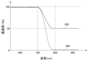
- 13 is a graph showing schematic wavelength characteristics of a first divided surface and a second divided surface in the fourth example.
- FIG. 1 is a diagram showing a schematic configuration of an imaging device 10 according to an embodiment.
- the imaging device 10 includes a first sensor 12, a second sensor 14, a third sensor 16, and a light splitting element 18.
- the imaging device 10 is a so-called three-chip camera, and is configured to split incident light 50 using the light splitting element 18 and capture images with the first sensor 12, the second sensor 14, and the third sensor 16, respectively.
- the light splitting element 18 comprises a first prism 22, a second prism 24, and a third prism 26.
- the light splitting element 18 is a so-called three-plate prism.
- the first prism 22 comprises a first entrance surface 28, a first splitting surface 30, and a first exit surface 32.
- the second prism 24 comprises a second entrance surface 34, a second splitting surface 36, and a second exit surface 38.
- the third prism 26 comprises a third entrance surface 40 and a third exit surface 42.
- An air gap is provided between the first splitting surface 30 and the second entrance surface 34.
- the incident light 50 incident on the first entrance surface 28 is split into a first reflected light 52 and a first transmitted light 54 at the first splitting surface 30.
- the first reflected light 52 reflected at the first splitting surface 30 is totally internally reflected at the first entrance surface 28, then passes through the first exit surface 32 and heads towards the first sensor 12.
- the first transmitted light 54 transmitted through the first splitting surface 30 is split into a second reflected light 56 and a second transmitted light 58 at the second splitting surface 36.
- the second reflected light 56 reflected at the second splitting surface 36 is totally internally reflected at the second entrance surface 34, then passes through the second exit surface 38 and heads towards the second sensor 14.
- the second transmitted light 58 transmitted through the second splitting surface 36 passes through the third entrance surface 40 and the third exit surface 42 and heads towards the third sensor 16.
- the first sensor 12 is a sensor that captures a first wavelength.
- One of the second sensor 14 and the third sensor 16 is a sensor that captures a first wavelength.
- the other of the second sensor 14 and the third sensor 16 is a sensor that captures a second wavelength different from the first wavelength. Therefore, two of the first sensor 12, the second sensor 14, and the third sensor 16 are sensors that capture the first wavelength, and the remaining one of the first sensor 12, the second sensor 14, and the third sensor 16 is a sensor that captures the second wavelength.
- the first wavelength is, for example, visible light
- the second wavelength is, for example, infrared light.
- the first wavelength may be infrared light
- the second wavelength may be visible light.
- the specific wavelengths of the first wavelength and the second wavelength are not particularly limited, and any wavelength in the wavelength range from ultraviolet light to infrared light may be selected.
- At least one of the first wavelength and the second wavelength may have a predetermined wavelength range. For example, when the first wavelength or the second wavelength is visible light, the first wavelength or the second wavelength may mean a part or the entire visible wavelength range from red to blue.
- the first sensor 12, the second sensor 14, and the third sensor 16 are visible light sensors that capture visible light or infrared light sensors that capture infrared light.
- the visible light sensor and the infrared light sensor have an imaging element that has a plurality of pixels.
- a two-dimensional image sensor such as a CCD (Charge Coupled Device) or a CMOS (Complementary Metal Oxide Semiconductor) can be used.
- the visible light sensor may be a color image sensor in which red (R), green (G), and blue (B) color filters are provided for each pixel.
- the visible light sensor may be a polarization sensor in which multiple types of polarizers with different polarization directions are provided for each pixel.
- the visible light sensor may be an event-based vision sensor (EVS) that outputs an image that extracts only pixels in which a change in luminance is detected.
- EVS event-based vision sensor
- the infrared light sensor may be a thermal image sensor for capturing a thermal image.
- the infrared light sensor may be a distance image sensor that measures the distance to an object using the ToF (Time of Flight) method.
- the first dividing surface 30 is configured to partially transmit and reflect the first wavelength and to completely transmit the second wavelength different from the first wavelength. That is, the first dividing surface 30 has partial transmittance and partial reflectance for the first wavelength and has total transmittance for the second wavelength.
- the first dividing surface 30 is configured to be a half mirror for the first wavelength and to be substantially total transmittance (i.e., non-reflective) for the second wavelength.
- Each of the first transmittance T1 and the first reflectance R1 of the first wavelength at the first dividing surface 30 is set within a range from a predetermined lower limit (e.g., 30%, 35%, 40%, or 45%) to a predetermined upper limit (e.g., 70%, 65%, 60%, or 55%), and is preferably 40% or more and 50% or less.
- the second transmittance T2 of the second wavelength at the first dividing surface 30 is greater than the first transmittance T1 and the first reflectance R1 of the first wavelength at the first dividing surface 30 and is greater than a predetermined upper limit (e.g., 70%).
- the second transmittance T2 of the second wavelength at the first dividing surface 30 is, for example, 90% or more, and preferably 95% or more.
- the second splitting surface 36 is configured to totally transmit one of the first and second wavelengths and totally reflect the other of the first and second wavelengths. That is, the second splitting surface 36 has total transparency for one of the first and second wavelengths and total reflectivity for the other of the first and second wavelengths.
- the second splitting surface 36 is a so-called dichroic mirror, which selectively transmits one of the first and second wavelengths and selectively reflects the other.
- the transmittance of one of the first and second wavelengths at the second splitting surface 36 is greater than the first transmittance T1 and first reflectance R1 of the first wavelength at the first splitting surface 30 and is greater than a predetermined upper limit (e.g., 70%).
- the transmittance of one of the first and second wavelengths at the second splitting surface 36 is, for example, 90% or more, and preferably 95% or more.
- the reflectance of the other of the first and second wavelengths at the second dividing surface 36 is greater than the first transmittance T1 and the first reflectance R1 of the first wavelength at the first dividing surface 30, and is greater than a predetermined upper limit (e.g., 70%).
- the reflectance of the other of the first and second wavelengths at the second dividing surface 36 is, for example, 90% or more, and preferably 95% or more.
- Each of the first split surface 30 and the second split surface 36 can be formed, for example, from a dielectric multilayer mirror. By adjusting the refractive index and thickness of each layer that constitutes the dielectric multilayer, it is possible to realize the first split surface 30 and the second split surface 36 that have the desired wavelength characteristics as described above.
- the amount of space available for placement varies depending on the position of the sensor.
- the third sensor 16 is placed in a position that does not interfere with the light splitting element 18, so there is ample space available for placement, and a sensor with a relatively large sensor size D3 can be placed therein.
- the second sensor 14 is close to the third prism 26, so there is little space available for placement, and only a sensor with a relatively small sensor size D2 can be placed therein.
- the first sensor 12 has more space available for placement than the second sensor 14, but interference with the third prism 26 must be taken into consideration, so there is less space available for placement than the third sensor 16. Therefore, the sensor size D1 that the first sensor 12 can take is larger than the sensor size D2 that the second sensor 14 can take, and smaller than the sensor size D3 that the third sensor 16 can take (i.e., D3>D1>D2).
- FIG. 2 is a table showing an example of optical characteristics of the imaging device 10 according to the embodiment and the comparative example.
- the transmittance is set to 100% when there is substantially total transmission (i.e., no reflection), 0% when there is substantially total reflection (i.e., no transmission), and 50% when there is partial transmission and reflection.
- the light intensity of the incident light on each of the first sensor 12, second sensor 14, and third sensor 16 is set to 100% when the light intensity of the incident light 50 is 100%, and the light loss due to passing through the light splitting element 18 is ignored.
- the transmittance of the first wavelength at the first dividing surface 30 is 50%, and the transmittance of the second wavelength at the first dividing surface 30 is 100%.
- the transmittance of the first wavelength at the second dividing surface 36 is 100%, and the transmittance of the second wavelength at the second dividing surface 36 is 0%.
- the transmittance of the first wavelength at the second dividing surface 36 is 0%, and the transmittance of the second wavelength at the second dividing surface 36 is 100%.
- the light intensity of the first wavelength incident on each of the first sensor 12 and the third sensor 16 is 50%, and the light intensity of the second wavelength incident on the second sensor 14 is 100%. Therefore, in the first embodiment, the first sensor 12 and the third sensor 16 are sensors that capture the first wavelength, and the second sensor 14 is a sensor that captures the second wavelength.
- the light intensity of the first wavelength incident on each of the first sensor 12 and the second sensor 14 is 50%, and the light intensity of the second wavelength incident on the third sensor 16 is 100%. Therefore, in the second embodiment, the first sensor 12 and the second sensor 14 are sensors that capture the first wavelength, and the third sensor 16 is a sensor that captures the second wavelength.
- a general half mirror and a dichroic mirror are combined as the first dividing surface 30 and the second dividing surface 36.
- the first dividing surface 30 is a dichroic mirror, and the second dividing surface 36 is a half mirror.
- the transmittance of the first wavelength at the first dividing surface 30 is 100%, and the transmittance of the second wavelength at the first dividing surface 30 is 0%.
- the transmittance of the first wavelength at the second dividing surface 36 is 50%, and the transmittance of the second wavelength at the second dividing surface 36 is 50%.
- the light intensity of the first wavelength incident on each of the second sensor 14 and the third sensor 16 is 50%, and the light intensity of the second wavelength incident on the first sensor 12 is 100%. Therefore, in Comparative Example 1, the second sensor 14 and the third sensor 16 are sensors that capture the first wavelength, and the first sensor 12 is a sensor that captures the second wavelength.
- the light intensity of the first wavelength incident on each of the two sensors that capture the first wavelength can be maximized (e.g., 50%), and the light intensity of the second wavelength incident on one sensor that captures the second wavelength can be maximized (e.g., 100%).
- the sensor that captures the second wavelength must be the first sensor 12.
- the first dividing surface 30 is a half mirror, and the second dividing surface 36 is a dichroic mirror.
- the transmittance of the first wavelength at the first dividing surface 30 is 50%, and the transmittance of the second wavelength at the first dividing surface 30 is 50%.
- the transmittance of the first wavelength at the second dividing surface 36 is 100%, and the transmittance of the second wavelength at the second dividing surface 36 is 0%.
- the transmittance of the first wavelength at the second dividing surface 36 is 0%, and the transmittance of the second wavelength at the second dividing surface 36 is 100%.
- the light intensity of the first wavelength incident on each of the first sensor 12 and the third sensor 16 is 50%, and the light intensity of the second wavelength incident on each of the first sensor 12 and the second sensor 14 is 50%.
- the light intensity of the first wavelength incident on each of the first sensor 12 and the second sensor 14 is 50%, and the light intensity of the second wavelength incident on each of the first sensor 12 and the third sensor 16 is 50%.
- the sensor that captures the second wavelength can be the first sensor 12 or the second sensor 14, and in Comparative Example 3, the sensor that captures the second wavelength can be the first sensor 12 or the third sensor 16, so there are fewer restrictions on placement.
- the light intensity of the second wavelength incident on the sensor that captures the second wavelength is about 50%, so the light intensity of the second wavelength incident on the sensor that captures the second wavelength cannot be maximized (e.g., 100%).
- the light intensity of the first wavelength incident on each of the two sensors that capture the first wavelength can be maximized (e.g., 50%), and the light intensity of the second wavelength incident on one sensor that captures the second wavelength can also be maximized (e.g., 100%).
- the sensor that captures the second wavelength can be disposed in the second sensor 14 or the third sensor 16. Therefore, according to the embodiment, the degree of freedom in sensor placement can be improved compared to Comparative Example 1, and the light intensity of the first or second wavelength incident on the three sensors can be maximized compared to Comparative Examples 2-3. According to the embodiment, it is possible to achieve both maximization of the light intensity incident on multiple sensors and the degree of freedom in placement of multiple sensors.
- the sensor that captures the second wavelength is the second sensor 14, so it is possible to use, for example, large sensors as the two sensors that capture the first wavelength.
- the sensor that captures the second wavelength is the third sensor 16, so it is possible to use, for example, a large sensor as the sensor that captures the second wavelength.
- (First embodiment) 3 is a graph showing the wavelength characteristics of the first divided surface 30A and the second divided surface 36A according to Example 1.
- the first example in FIG. 3 corresponds to the above-mentioned first embodiment in which the first wavelength is visible light of 700 nm or less and the second wavelength is infrared light of 800 nm or more.
- the first divided surface 30A has a first transmittance for the first wavelength (visible light) of approximately 50% (e.g., 45% to 50%) and a second transmittance for the second wavelength (infrared light) of approximately 100% (e.g., 95% to 100%).
- the first divided surface 30A has a first reflectance for the first wavelength (visible light) of approximately 50% (e.g., 45% to 50%) and a second reflectance for the second wavelength (infrared light) of approximately 0% (e.g., 0% to 5%).
- the second split surface 36A has a transmittance of approximately 100% (e.g., 95% to 100%) for the first wavelength (visible light) and a transmittance of approximately 0% (e.g., 0% to 5%) for the second wavelength (infrared light).
- the second split surface 36A has a reflectance of approximately 0% (e.g., 0% to 5%) for the first wavelength (visible light) and a reflectance of approximately 100% (e.g., 95% to 100%) for the second wavelength (infrared light).
- approximately 50% of the light intensity of the first wavelength (visible light) of the incident light 50 can be incident on each of the first sensor 12 and the third sensor 16, and approximately 100% of the light intensity of the second wavelength (infrared light) of the incident light 50 can be incident on the second sensor 14.
- the first sensor 12 and the third sensor 16 are visible light sensors, and the second sensor 14 is an infrared light sensor. According to the first embodiment, it is possible to maximize the light intensity of the visible light incident on each of the first sensor 12 and the third sensor 16, and to maximize the light intensity of the infrared light incident on the second sensor 14. The first embodiment is effective when attempting to increase the sensor size of the two visible light sensors.
- the first sensor 12 can be a color image sensor
- the second sensor 14 can be a distance image sensor
- the third sensor 16 can be a polarization sensor or an EVS.
- the available sensor size of the polarization sensor or the EVS may be limited, and the sensor size may be relatively large.
- the third sensor 16, which has the most space for placement can be a polarization sensor or an EVS.
- the distance image sensor may have a smaller number of pixels and a relatively smaller sensor size than other sensors.
- the second sensor 14, which has the most limited space for placement can be a distance image sensor. This allows the first sensor 12, which has more space for placement than the second sensor 14, to be a color image sensor. As a result, a color image sensor with a larger sensor size can be used compared to when the second sensor 14 is a color image sensor.
- Second Example 4 is a graph showing the wavelength characteristics of the first divided surface 30B and the second divided surface 36B according to Example 2.
- Example 2 in FIG. 4 corresponds to the above-mentioned first embodiment in which the first wavelength is infrared light of 800 nm or more and the second wavelength is visible light of 700 nm or less.
- the first divided surface 30B has a first transmittance for the first wavelength (infrared light) of approximately 50% (e.g., 45% to 50%) and a second transmittance for the second wavelength (visible light) of approximately 100% (e.g., 95% to 100%).
- the first divided surface 30B has a first reflectance for the first wavelength (infrared light) of approximately 50% (e.g., 45% to 50%) and a second reflectance for the second wavelength (visible light) of approximately 0% (e.g., 0% to 5%).
- the second split surface 36B has a transmittance of approximately 100% (e.g., 95% to 100%) for the first wavelength (infrared light) and a transmittance of approximately 0% (e.g., 0% to 5%) for the second wavelength (visible light).
- the second split surface 36B has a reflectance of approximately 0% (e.g., 0% to 5%) for the first wavelength (infrared light) and a reflectance of approximately 100% (e.g., 95% to 100%) for the second wavelength (visible light).
- approximately 50% of the light intensity of the first wavelength (infrared light) of the incident light 50 can be incident on each of the first sensor 12 and the third sensor 16, and approximately 100% of the light intensity of the second wavelength (visible light) of the incident light 50 can be incident on the second sensor 14.
- the first sensor 12 and the third sensor 16 are infrared light sensors, and the second sensor 14 is a visible light sensor.
- the first embodiment it is possible to maximize the light intensity of the infrared light incident on each of the first sensor 12 and the third sensor 16, and to maximize the light intensity of the visible light incident on the second sensor 14.
- the second embodiment is effective when attempting to make the size of the two infrared light sensors as large as possible.
- the first sensor 12 can be a distance image sensor, the second sensor 14 a color image sensor, and the third sensor 16 a thermal image sensor.
- (Third Example) 5 is a graph showing the wavelength characteristics of the first divided surface 30C and the second divided surface 36C according to Example 3.
- Example 3 in FIG. 5 corresponds to the second embodiment described above in which the first wavelength is visible light of 700 nm or less and the second wavelength is infrared light of 800 nm or more.
- the first divided surface 30C is similar to the first divided surface 30A in the first embodiment.
- the first divided surface 30C has a first transmittance for the first wavelength (visible light) of approximately 50% (e.g., 45% to 50%) and a second transmittance for the second wavelength (infrared light) of approximately 100% (e.g., 95% to 100%).
- the first divided surface 30C has a first reflectance for the first wavelength (visible light) of approximately 50% (e.g., 45% to 50%) and a second reflectance for the second wavelength (infrared light) of approximately 0% (e.g., 0% to 5%).
- the second divided surface 36C corresponds to the second divided surface 36A of the first embodiment with the reflectance and transmittance reversed.
- the second divided surface 36C has a transmittance of about 0% (e.g., 0% to 5%) for the first wavelength (visible light) and a transmittance of about 100% (e.g., 95% to 100%) for the second wavelength (infrared light).
- the second divided surface 36C has a reflectance of about 100% (e.g., 95% to 100%) for the first wavelength (visible light) and a reflectance of about 0% (e.g., 0% to 5%) for the second wavelength (infrared light).
- approximately 50% of the light intensity of the first wavelength (visible light) of the incident light 50 can be incident on each of the first sensor 12 and the second sensor 14, and approximately 100% of the light intensity of the second wavelength (infrared light) of the incident light 50 can be incident on the third sensor 16.
- the first sensor 12 and the second sensor 14 are visible light sensors
- the third sensor 16 is an infrared light sensor. According to the third embodiment, it is possible to maximize the light intensity of the visible light incident on each of the first sensor 12 and the second sensor 14, and to maximize the light intensity of the infrared light incident on the third sensor 16.
- the third embodiment is effective when attempting to make the size of one infrared light sensor as large as possible.
- the first sensor 12 can be a polarization sensor or EVS
- the second sensor 14 can be a color image sensor
- the third sensor 16 can be a thermal image sensor or a distance image sensor.
- (Fourth Example) 6 is a graph showing the wavelength characteristics of the first divided surface 30D and the second divided surface 36D according to Example 4.
- Example 4 in FIG. 6 corresponds to the second embodiment described above, in which the first wavelength is infrared light of 800 nm or more and the second wavelength is visible light of 700 nm or less.
- the first divided surface 30D is similar to the first divided surface 30B in the second embodiment.
- the first divided surface 30D has a first transmittance for the first wavelength (infrared light) of approximately 50% (e.g., 45% to 50%) and a second transmittance for the second wavelength (visible light) of approximately 100% (e.g., 95% to 100%).
- the first divided surface 30D has a first reflectance for the first wavelength (infrared light) of approximately 50% (e.g., 45% to 50%) and a second reflectance for the second wavelength (visible light) of approximately 0% (e.g., 0% to 5%).
- the second dividing surface 36D corresponds to the second dividing surface 36C of the third embodiment with its reflectance and transmittance reversed.
- the second dividing surface 36D has a transmittance of approximately 0% (e.g., 0% to 5%) for the first wavelength (infrared light) and a transmittance of approximately 100% (e.g., 95% to 100%) for the second wavelength (visible light).
- the second dividing surface 36D has a reflectance of approximately 100% (e.g., 95% to 100%) for the first wavelength (infrared light) and a reflectance of approximately 0% (e.g., 0% to 5%) for the second wavelength (visible light).
- approximately 50% of the light intensity of the first wavelength (infrared light) of the incident light 50 can be incident on each of the first sensor 12 and the second sensor 14, and approximately 100% of the light intensity of the second wavelength (visible light) of the incident light 50 can be incident on the third sensor 16.
- the first sensor 12 and the second sensor 14 are infrared light sensors
- the third sensor 16 is a visible light sensor. According to the fourth embodiment, it is possible to maximize the light intensity of the infrared light incident on each of the first sensor 12 and the second sensor 14, and to maximize the light intensity of the visible light incident on the third sensor 16.
- the third embodiment is effective when attempting to make the size of one visible light sensor as large as possible.
- the first sensor 12 can be a thermal image sensor
- the second sensor 14 can be a distance image sensor
- the third sensor 16 can be a color image sensor, a polarization sensor, or an EVS.
- the present invention makes it possible to maximize the light intensity incident on multiple sensors while allowing freedom in the placement of the multiple sensors.
Landscapes
- Engineering & Computer Science (AREA)
- Multimedia (AREA)
- Signal Processing (AREA)
- Human Computer Interaction (AREA)
- Physics & Mathematics (AREA)
- General Physics & Mathematics (AREA)
- Optics & Photonics (AREA)
- Photometry And Measurement Of Optical Pulse Characteristics (AREA)
Priority Applications (2)
| Application Number | Priority Date | Filing Date | Title |
|---|---|---|---|
| JP2024552425A JPWO2024185372A1 (https=) | 2023-03-09 | 2024-02-07 | |
| US19/314,328 US20250386086A1 (en) | 2023-03-09 | 2025-08-29 | Imaging apparatus |
Applications Claiming Priority (2)
| Application Number | Priority Date | Filing Date | Title |
|---|---|---|---|
| JP2023036632 | 2023-03-09 | ||
| JP2023-036632 | 2023-03-09 |
Related Child Applications (1)
| Application Number | Title | Priority Date | Filing Date |
|---|---|---|---|
| US19/314,328 Continuation US20250386086A1 (en) | 2023-03-09 | 2025-08-29 | Imaging apparatus |
Publications (1)
| Publication Number | Publication Date |
|---|---|
| WO2024185372A1 true WO2024185372A1 (ja) | 2024-09-12 |
Family
ID=92674424
Family Applications (1)
| Application Number | Title | Priority Date | Filing Date |
|---|---|---|---|
| PCT/JP2024/003999 Ceased WO2024185372A1 (ja) | 2023-03-09 | 2024-02-07 | 撮像装置 |
Country Status (3)
| Country | Link |
|---|---|
| US (1) | US20250386086A1 (https=) |
| JP (1) | JPWO2024185372A1 (https=) |
| WO (1) | WO2024185372A1 (https=) |
Citations (3)
| Publication number | Priority date | Publication date | Assignee | Title |
|---|---|---|---|---|
| JP2019200404A (ja) * | 2018-05-15 | 2019-11-21 | 株式会社三井光機製作所 | 光学モジュール及び光学装置 |
| JP2021175000A (ja) * | 2020-04-17 | 2021-11-01 | パナソニックi−PROセンシングソリューションズ株式会社 | 3板式カメラおよび4板式カメラ |
| WO2022044897A1 (ja) * | 2020-08-31 | 2022-03-03 | ソニーグループ株式会社 | 医療撮像システム、医療撮像装置、および動作方法 |
-
2024
- 2024-02-07 JP JP2024552425A patent/JPWO2024185372A1/ja active Pending
- 2024-02-07 WO PCT/JP2024/003999 patent/WO2024185372A1/ja not_active Ceased
-
2025
- 2025-08-29 US US19/314,328 patent/US20250386086A1/en active Pending
Patent Citations (3)
| Publication number | Priority date | Publication date | Assignee | Title |
|---|---|---|---|---|
| JP2019200404A (ja) * | 2018-05-15 | 2019-11-21 | 株式会社三井光機製作所 | 光学モジュール及び光学装置 |
| JP2021175000A (ja) * | 2020-04-17 | 2021-11-01 | パナソニックi−PROセンシングソリューションズ株式会社 | 3板式カメラおよび4板式カメラ |
| WO2022044897A1 (ja) * | 2020-08-31 | 2022-03-03 | ソニーグループ株式会社 | 医療撮像システム、医療撮像装置、および動作方法 |
Also Published As
| Publication number | Publication date |
|---|---|
| US20250386086A1 (en) | 2025-12-18 |
| JPWO2024185372A1 (https=) | 2024-09-12 |
Similar Documents
| Publication | Publication Date | Title |
|---|---|---|
| KR102201627B1 (ko) | 고체 촬상 소자 및 촬상 장치 | |
| US8134191B2 (en) | Solid-state imaging device, signal processing method, and camera | |
| JP2552856B2 (ja) | ビ−ムスプリツタ | |
| JP5001471B1 (ja) | 撮像装置、撮像システム、及び撮像方法 | |
| US20150177599A1 (en) | Illumination system and projection device comprising the same | |
| US7550709B2 (en) | Solid-state imaging device and method for fabricating the same | |
| EP1845559A1 (en) | Solid-state imaging device, camera and signal processing method | |
| CN102714738A (zh) | 固体摄像元件和摄像装置 | |
| JP2006238093A (ja) | 撮像装置 | |
| AU2011307151A1 (en) | Digital multi-spectral camera system having at least two independent digital cameras | |
| JP2009086165A (ja) | 色分解光学系および撮像装置 | |
| CN103477436B (zh) | 摄像装置 | |
| JP6525603B2 (ja) | 撮像装置 | |
| US11378810B2 (en) | Polygon x-prism for imaging and display applications | |
| US20190162976A1 (en) | Multi-way prism | |
| JP4506678B2 (ja) | プリズム光学系および撮像装置 | |
| WO2024185372A1 (ja) | 撮像装置 | |
| US8659833B2 (en) | Color separating optical system and image pickup apparatus including the same | |
| JP2002296414A (ja) | 光学素子、それを用いた液晶プロジェクター及びカメラ | |
| JP5171993B2 (ja) | 2板撮像装置 | |
| WO2024135060A1 (ja) | 撮像装置 | |
| JP6559007B2 (ja) | 色分解光学系及びそれを有する撮像装置 | |
| JP2017037162A5 (https=) | ||
| JP2006091653A (ja) | 色分解光学系 | |
| JP2006178264A (ja) | 色分解光学系 |
Legal Events
| Date | Code | Title | Description |
|---|---|---|---|
| WWE | Wipo information: entry into national phase |
Ref document number: 2024552425 Country of ref document: JP |
|
| 121 | Ep: the epo has been informed by wipo that ep was designated in this application |
Ref document number: 24766747 Country of ref document: EP Kind code of ref document: A1 |
|
| NENP | Non-entry into the national phase |
Ref country code: DE |
|
| 122 | Ep: pct application non-entry in european phase |
Ref document number: 24766747 Country of ref document: EP Kind code of ref document: A1 |