WO2024185293A1 - 発振回路 - Google Patents
発振回路 Download PDFInfo
- Publication number
- WO2024185293A1 WO2024185293A1 PCT/JP2024/000603 JP2024000603W WO2024185293A1 WO 2024185293 A1 WO2024185293 A1 WO 2024185293A1 JP 2024000603 W JP2024000603 W JP 2024000603W WO 2024185293 A1 WO2024185293 A1 WO 2024185293A1
- Authority
- WO
- WIPO (PCT)
- Prior art keywords
- oscillator
- current
- frequency
- circuit
- oscillation
- Prior art date
- Legal status (The legal status is an assumption and is not a legal conclusion. Google has not performed a legal analysis and makes no representation as to the accuracy of the status listed.)
- Ceased
Links
Images











Classifications
-
- H—ELECTRICITY
- H03—ELECTRONIC CIRCUITRY
- H03K—PULSE TECHNIQUE
- H03K3/00—Circuits for generating electric pulses; Monostable, bistable or multistable circuits
- H03K3/02—Generators characterised by the type of circuit or by the means used for producing pulses
- H03K3/027—Generators characterised by the type of circuit or by the means used for producing pulses by the use of logic circuits, with internal or external positive feedback
- H03K3/03—Astable circuits
-
- H—ELECTRICITY
- H03—ELECTRONIC CIRCUITRY
- H03K—PULSE TECHNIQUE
- H03K3/00—Circuits for generating electric pulses; Monostable, bistable or multistable circuits
- H03K3/02—Generators characterised by the type of circuit or by the means used for producing pulses
- H03K3/353—Generators characterised by the type of circuit or by the means used for producing pulses by the use, as active elements, of field-effect transistors with internal or external positive feedback
- H03K3/354—Astable circuits
-
- H—ELECTRICITY
- H03—ELECTRONIC CIRCUITRY
- H03L—AUTOMATIC CONTROL, STARTING, SYNCHRONISATION OR STABILISATION OF GENERATORS OF ELECTRONIC OSCILLATIONS OR PULSES
- H03L7/00—Automatic control of frequency or phase; Synchronisation
- H03L7/06—Automatic control of frequency or phase; Synchronisation using a reference signal applied to a frequency- or phase-locked loop
-
- H—ELECTRICITY
- H03—ELECTRONIC CIRCUITRY
- H03L—AUTOMATIC CONTROL, STARTING, SYNCHRONISATION OR STABILISATION OF GENERATORS OF ELECTRONIC OSCILLATIONS OR PULSES
- H03L7/00—Automatic control of frequency or phase; Synchronisation
- H03L7/06—Automatic control of frequency or phase; Synchronisation using a reference signal applied to a frequency- or phase-locked loop
- H03L7/08—Details of the phase-locked loop
- H03L7/099—Details of the phase-locked loop concerning mainly the controlled oscillator of the loop
Definitions
- This technology relates to an oscillator circuit. More specifically, this technology relates to an oscillator circuit capable of stabilizing an oscillation frequency based on a frequency locked loop (FLL).
- FLL frequency locked loop
- Various oscillators such as LC oscillators and ring oscillators, are used to generate clocks and the like.
- a PLL Phase Locked Loop
- LC oscillators and ring oscillators are used to generate clocks and the like.
- PLL Phase Locked Loop
- a PLL Phase Locked Loop
- This technology was developed in light of these circumstances, and aims to alleviate the operational constraints of oscillator circuits that use feedback loops.
- the present technology has been made to solve the above-mentioned problems, and its first aspect is an oscillation circuit including an oscillator and a current feedback section that configures a feedback loop for the oscillator based on a current into which the oscillation frequency of the oscillator is converted. This provides the effect of configuring a feedback loop for the oscillator without comparing a voltage according to the oscillation frequency of the oscillator.
- the current feedback unit may include a frequency-current conversion unit that converts the oscillation frequency of the oscillator into a current, and a differential current generation unit that generates a differential current between the current generated by the frequency-current conversion unit and a reference current. This provides the effect of converting an increase or decrease in the oscillation frequency of the oscillator into an increase or decrease in impedance.
- the frequency-to-current converter may include a switched capacitor that generates a current according to the oscillation frequency. This provides the effect of converting the oscillation frequency of the oscillator into a current based on a switching operation.
- the switched capacitor may include a variable capacitance element. This provides the effect of realizing frequency adjustment using the switched capacitor.
- the differential current generating unit may include a cascode current mirror circuit that receives as input the current generated by the switched capacitor and the reference current. This provides the effect of generating a differential current based on impedance conversion of the oscillation frequency of the oscillator.
- the device may further include a reference resistor used to generate the reference current, and a compensation resistor connected in series to the switched capacitor and having a temperature characteristic different from that of the reference resistor. This provides the effect of compensating for the temperature characteristic of the FLL.
- a chopper circuit may be further provided that alternately switches the output destination of the current generated by the switched capacitor and the output destination of the reference current. This provides the effect of eliminating mismatches between mirror transistors used in the current mirror based on the switching operation.
- the differential current generating unit may include a current mirror circuit that receives the current generated by the switched capacitor as an input. This provides the effect of generating a differential current based on impedance conversion of the oscillation frequency of the oscillator.
- the current mirror circuit may further include a reference resistor used to generate the reference current, and a diode-connected transistor connected in series to the reference resistor and having characteristics equivalent to those of a diode-connected mirror transistor in the current mirror circuit. This provides the effect of matching the impedance of the current path of the reference current and the current path of the current flowing through the mirror transistor of the current mirror circuit.
- a compensation resistor having temperature characteristics different from those of the reference resistor may be further provided, which is connected in series with the mirror transistor of the current mirror circuit. This provides the effect of compensating for the temperature characteristics of the FLL.
- the device may further include a bootstrap circuit used for switching the switched capacitor. This reduces the on-resistance of the switched capacitor when it is switched.
- the clock may be used as a reference clock source for an integrated circuit. This has the effect of stabilizing the operation of the integrated circuit that operates based on a clock.
- the integrated circuit may be integrated into a semiconductor chip on which the integrated circuit is formed. This has the effect of eliminating the need for an external oscillator to supply a clock to the integrated circuit.
- the oscillator may be an LC oscillator or a ring oscillator. This provides the effect of forming a feedback type oscillator circuit using a PLL.
- the second aspect is an oscillation circuit including an oscillator, a frequency synchronization unit that configures a feedback loop for the oscillator based on the oscillation frequency of the oscillator, and a PLL (Phase Locked Loop) connected downstream of the oscillator. This has the effect of stabilizing the oscillation frequency of the oscillator connected upstream of the PLL.
- PLL Phase Locked Loop
- the frequency synchronization unit may include a frequency-voltage conversion unit that generates a control voltage according to the oscillation frequency of the oscillator. This provides the effect of controlling the oscillation frequency of the oscillator based on the oscillation frequency of the oscillator.
- the frequency-voltage conversion unit may include a switched capacitor that generates a voltage according to the oscillation frequency of the oscillator, an amplifier that generates a difference between the voltage generated by the switched capacitor and a reference voltage, and a low-pass filter that extracts low-frequency components from the output of the amplifier. This provides the effect of generating a control voltage used to control the oscillation frequency of the oscillator based on the oscillation frequency of the oscillator.
- a parameter correction unit may be further provided that corrects parameters used to control the PLL based on the detection result of the control voltage of the oscillator output from the frequency synchronization unit. This provides the effect of stabilizing the operating frequency of the PLL connected downstream of the oscillator while stabilizing the oscillation frequency of the oscillator based on the FLL.
- the parameter correction unit may include a power supply voltage correction value calculation unit that calculates a correction value for the power supply voltage of the frequency synchronization unit, a control voltage correction value calculation unit that calculates a correction value for the control voltage of the oscillator, and a temperature correction value calculation unit that calculates a correction value for the temperature of the frequency synchronization unit, and may correct the parameters based on the power supply voltage correction value, the control voltage correction value, and the temperature correction value.
- This provides the effect of stabilizing the oscillation frequency of the oscillator based on the FLL while stabilizing the operating frequency of the PLL in accordance with the operating environment of the FLL.
- the third aspect is an oscillation circuit including an oscillator, a PLL (Phase Locked Loop) connected downstream of the oscillator, a frequency-voltage conversion unit that generates a voltage corresponding to the oscillation frequency of the oscillator, and a parameter correction unit that corrects parameters used to control the PLL based on the voltage generated by the frequency-voltage conversion unit.
- PLL Phase Locked Loop
- This provides the effect of stabilizing the operating frequency of the PLL while using the oscillator as the source oscillation circuit of the PLL.
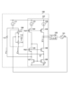
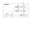
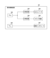
- FIG. 1 is a block diagram showing a configuration example of an oscillator circuit according to a first embodiment
- 1 is a circuit diagram illustrating a configuration example of an oscillator circuit according to a first embodiment
- FIG. 2 is a circuit diagram illustrating a first example of an oscillator according to a first embodiment
- FIG. 4 is a circuit diagram illustrating a second example of the oscillator according to the first embodiment.
- FIG. 11 is a circuit diagram illustrating a configuration example of an oscillator circuit according to a second embodiment.
- FIG. 13 is a circuit diagram illustrating a configuration example of an oscillator circuit according to a third embodiment.
- FIG. 13 is a circuit diagram illustrating a configuration example of an oscillator circuit according to a fourth embodiment.
- FIG. 13 is a circuit diagram illustrating a configuration example of an oscillator circuit according to a fifth embodiment.
- FIG. 13 is a circuit diagram illustrating a configuration example of an oscillator circuit according to a sixth embodiment.
- FIG. 23 is a circuit diagram illustrating a first example of a chopper circuit according to a sixth embodiment.
- FIG. 23 is a circuit diagram illustrating a second example of a chopper circuit according to the sixth embodiment.
- 13 is a timing chart showing a chopper operation of the oscillator circuit according to the sixth embodiment.
- FIG. 13 is a block diagram illustrating a configuration example of a solid-state imaging device to which an oscillator circuit according to a seventh embodiment is applied.
- FIG. 13 is a block diagram illustrating an example of the configuration of a solid-state imaging device to which an oscillator circuit according to an eighth embodiment is applied.
- FIG. 23 is a block diagram illustrating an example of the configuration of a solid-state imaging device to which an oscillator circuit according to a ninth embodiment is applied.
- FIG. 23 is a block diagram illustrating a configuration example of a solid-state imaging device to which an oscillator circuit according to a tenth embodiment is applied.
- FIG. 23 is a block diagram showing a configuration example of a solid-state imaging device to which an oscillator circuit according to an eleventh embodiment is applied.
- FIG. 23 is a block diagram showing a configuration example of a solid-state imaging device to which an oscillator circuit according to a twelfth embodiment is applied.
- FIG. 23 is a block diagram showing a configuration example of a solid-state imaging device to which an oscillator circuit according to a thirteenth embodiment is applied.
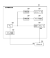
- FIG. 23 is a block diagram showing a configuration example of an oscillator circuit according to a fourteenth embodiment.
- FIG. 23 is a diagram illustrating the relationship between the operating environment and the oscillation frequency of the oscillator circuit according to the fourteenth embodiment.
- FIG. 23 is a circuit diagram illustrating a configuration example of an oscillator circuit according to a fifteenth embodiment.
- FIG. 23 is a diagram showing the state of each part during operation of the oscillator circuit according to the fifteenth embodiment.
- FIG. 23 is a circuit diagram showing a configuration example of an oscillator circuit according to a sixteenth embodiment.
- FIG. 23 is a circuit diagram showing a configuration example of an oscillator circuit according to a seventeenth embodiment.
- FIG. 23 is a perspective view showing an example of a stack of layers in a solid-state imaging device according to an eighteenth embodiment.
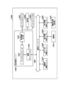
- 1 is a block diagram showing a schematic configuration example of a vehicle control system;
- FIG. 4 is an explanatory diagram showing an example of an installation position of an imaging unit.
- First embodiment an example in which current feedback is performed based on a comparison result with a reference current in an FLL
- Second embodiment an example of performing temperature compensation of an FLL in which current feedback is performed based on a comparison result with a reference current
- Third embodiment example of current feedback without comparison with reference current in FLL
- Fourth embodiment an example of performing temperature compensation of an FLL in which current feedback is performed without performing a comparison with a reference current
- Fifth embodiment (example of using a bootstrap circuit for switching a switched capacitor) 6.
- Eleventh embodiment an example in which a PLL used in an AD converter, a logic circuit, and a communication interface is provided after an FLL
- Twelfth embodiment an example in which an FLL used in an AD converter and a logic circuit and an FLL used in a communication interface are provided
- Thirteenth embodiment an example in which the frequency of an FLL used in a solid-state imaging device can be externally controlled
- Fourteenth embodiment an example in which an FLL is used as a source oscillation circuit of a PLL, and the frequency of the PLL can be corrected based on a detection value related to the oscillation frequency of the FLL
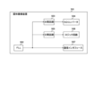
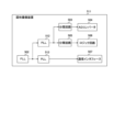
- FIG. 1 is a block diagram showing an example of the configuration of an oscillator circuit according to a first embodiment.
- the oscillation circuit includes an oscillator 101, a current feedback section 102, and a loop filter 103. At this time, the oscillation circuit can operate as an FLL.
- the oscillator 101 generates an oscillation signal Sc based on an oscillation operation.
- the oscillator 101 can change the oscillation frequency fs based on voltage control.
- the oscillator 101 may be a ring oscillator or an LC oscillator.
- the current feedback unit 102 forms a feedback loop for the oscillator 101 based on the current Ic into which the oscillation frequency fs of the oscillator 101 is converted.
- the current feedback unit 102 includes a frequency-current conversion unit 104 and a differential current generation unit 105.
- the frequency-to-current converter 104 converts the oscillation frequency fs of the oscillator 101 into a current Ic.
- the frequency-to-current converter 104 may include a switched capacitor that generates a current Ic according to the oscillation frequency fs of the oscillator 101. Note that the oscillation frequency fs of the oscillator 101 may be divided.
- the differential current generating unit 105 generates a differential current Is between the current Ic generated by the frequency-to-current converting unit 104 and a reference current Ir.
- the differential current generating unit 105 may include a cascode current mirror circuit that receives the current Ic generated by the switched capacitor and the reference current Ir as input, or may include a current mirror circuit that receives the current Ic generated by the switched capacitor as input.
- the loop filter 103 applies a control voltage to the oscillator 101 that corresponds to the differential current Is output from the current feedback section 102.
- FIG. 2 is a circuit diagram showing an example of the configuration of an oscillator circuit according to the first embodiment.
- the current feedback section 102 includes a switched capacitor 106, a cascode current mirror circuit 107, a current source 111, and a reference resistor 112.
- the switched capacitor 106 generates a current Ic according to the oscillation frequency fs of the oscillator 101 based on a switching operation.
- the switched capacitor 106 includes switches 113 and 114 and a capacitor 115.
- the switches 113 and 114 are connected in series with each other, and a capacitor 115 is connected to the connection point. Each switch 113 and 114 is switched based on the oscillation frequency fs of the oscillator 101. At this time, the switching of each switch 113 and 114 is set to be in opposite phase to each other.
- the switches 113 and 114 may be field effect transistors.
- the switched capacitor 106 is connected in parallel to the reference resistor 112 with respect to the current source 111. The switched capacitor 106 outputs a current Ic according to the oscillation frequency fs of the oscillator 101 to the cascode current mirror circuit 107.
- the reference resistor 112 generates a reference current Ir based on the current supplied from the current source 111 and outputs it to the cascode current mirror circuit 107.
- Cascode current mirror circuit 107 receives current Ic generated by switched capacitor 106 and reference current Ir as inputs, and generates a difference current Is between them.
- Cascode current mirror circuit 107 includes mirror transistors 123 to 128 and current sources 121 and 122.
- Mirror transistors 123 and 124 may be P-channel field effect transistors, and mirror transistors 125 to 128 may be N-channel field effect transistors.
- Current source 121 and mirror transistors 123, 125, 127 are connected in series, and current source 122 and mirror transistors 124, 126, 128 are connected in series.
- a bias voltage Vb1 is input to the gates of mirror transistors 123, 124, and a bias voltage Vb2 is input to the gates of mirror transistors 125, 126.
- the gates of mirror transistors 127, 128 are connected to the connection point of mirror transistors 123, 125.
- the connection point of mirror transistors 125, 127 is connected to reference resistor 112.
- the connection point of mirror transistors 126, 128 is connected to switched capacitor 106.
- the connection point of mirror transistors 124, 126 is connected to loop filter 103.
- switched capacitor 106 In switched capacitor 106, when switch 113 is on and switch 114 is off, current is supplied from current source 111 to capacitor 115 via switch 113, and charge is accumulated in capacitor 115. When switch 113 is off and switch 114 is on, the charge accumulated in capacitor 115 is discharged via switch 114, and current Ic generated in switched capacitor 106 is supplied to mirror transistor 128.
- the oscillation frequency fs of oscillator 101 increases, the number of times the charge accumulated in capacitor 115 is discharged increases, and current Ic generated in switched capacitor 106 increases.
- switched capacitor 106 can be regarded as the impedance of resistor R, and if the capacitance value of capacitor 115 is C, resistance R of switched capacitor 106 can be given by the formula 1/(fs ⁇ C). Therefore, when the oscillation frequency fs of the oscillator 101 increases, the resistance R of the switched capacitor 106 decreases, but because the switched capacitor 106 and the reference resistor 112 are driven by the current source 111, the total current does not change and the power does not increase.
- the current Ic generated by the switched capacitor 106 is supplied to the mirror transistor 128, and the reference current Ir generated by the reference resistor 112 is supplied to the mirror transistor 127.
- the reference current Ir flows through the mirror transistor 128 based on the current mirror operation of the mirror transistors 127 and 128.
- the reference current Ir is subtracted from the current Ic supplied by the switched capacitor 106 to generate a differential current Is, which flows through the mirror transistor 126.
- This differential current Is is extracted from the loop filter 103, and the control voltage of the oscillator 101 changes according to the differential current Is, and the oscillation frequency fs of the oscillator 101 changes.
- the oscillator 101 enters a steady state.
- the switched capacitor 106 is regarded as an impedance
- the resistance R is equal to the resistance value Rr of the reference resistor 112
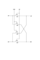
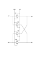
- FIG. 3 is a circuit diagram showing a first example of an oscillator according to the first embodiment. Note that in this figure, an example of the oscillator is a ring oscillator.
- the ring oscillator is made up of multiple (odd number) inverters 131 connected in multiple stages, with the output of the last inverter being fed back to the input of the first inverter.
- FIG. 4 is a circuit diagram showing a second example of an oscillator according to the first embodiment. Note that in this figure, an example of an oscillator is shown as an LC oscillator.
- the LC oscillator generates an oscillation signal based on the resonance of inductor 141 and capacitor 142.
- the oscillation signal is a differential output signal.
- the LC oscillator includes inductor 141, capacitor 142, transistors 143 and 144, and current source 145.
- Transistors 143 and 144 are N-channel field effect transistors.
- Inductor 141 and capacitor 142 are connected in parallel to each other.
- the drains of transistors 143 and 144 are connected to both ends of capacitor 142.
- the drain of transistor 143 is connected to the gate of transistor 144, and the drain of transistor 144 is connected to the gate of transistor 143.
- the sources of transistors 143 and 144 are connected to the ground potential via current source 145.
- a reference resistor 112 in order to perform current feedback in the FLL, a reference resistor 112 is provided to generate a reference current Ir.
- a compensation resistor in order to achieve temperature compensation while performing current feedback in the FLL, a compensation resistor having temperature characteristics different from those of the reference resistor 112 is provided.
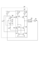
- FIG. 5 is a circuit diagram showing an example of the configuration of an oscillator circuit according to the second embodiment.
- this oscillator circuit has a current feedback section 152 instead of the current feedback section 102 of the first embodiment described above.
- the rest of the configuration of the oscillator circuit of the second embodiment is the same as the configuration of the oscillator circuit of the first embodiment described above.
- the current feedback section 152 is the current feedback section 102 of the first embodiment described above to which a compensation resistor 116 has been added.
- the rest of the configuration of the current feedback section 152 is the same as the configuration of the current feedback section 102 of the first embodiment described above.
- the compensation resistor 116 has a different temperature characteristic from the reference resistor 112.
- the temperature characteristic of the compensation resistor 116 can be set so that the temperature characteristic of the reference resistor 112 is compensated for.
- the compensation resistor 116 is connected in series with the switched capacitor 106.
- the resistance value of the compensation resistor 116 is R'
- the resistance R when the switched capacitor 106 is regarded as an impedance is equal to Rr-R'
- the compensation resistor 116 which has a temperature characteristic different from that of the reference resistor 112, is connected in series to the switched capacitor 106.
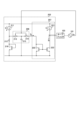
- FIG. 6 is a circuit diagram showing an example of the configuration of an oscillator circuit according to the third embodiment.
- this oscillator circuit has a current feedback section 202 instead of the current feedback section 102 of the first embodiment described above.
- the rest of the configuration of the oscillator circuit of the third embodiment is the same as the configuration of the oscillator circuit of the first embodiment described above.
- the current feedback section 202 includes a switched capacitor 206, a current mirror circuit 207, a current source 211, a reference resistor 212, and a diode-connected transistor 216.
- the switched capacitor 206 generates a current Ic according to the oscillation frequency fs of the oscillator 101 based on a switching operation.
- the switched capacitor 206 includes switches 213 and 214 and a capacitor 215.
- the switches 213 and 214 are connected in series with each other, and a capacitor 215 is connected to the connection point between them. Each switch 213 and 214 is switched based on the oscillation frequency fs of the oscillator 101. At this time, the switching of each switch 213 and 214 is set to be in opposite phase to each other.
- the switched capacitor 206 is connected to the connection point between the current source 211 and the reference resistor 212. The switched capacitor 206 outputs a current Ic according to the oscillation frequency fs of the oscillator 101 to the current mirror circuit 207.
- Reference source 211 generates reference current Ir.
- Reference resistor 212 is connected in series to current source 211.
- Diode-connected transistor 216 is connected in series to reference resistor 212.
- Diode-connected transistor 216 can have characteristics equivalent to those of mirror transistor 222 of current mirror circuit 207. In this case, diode-connected transistor 216 can match the impedance of the path through which reference current Ir flows with the impedance of the path through which current Ic generated by switched capacitor 106 flows.
- An N-channel field effect transistor may be used as diode-connected transistor 216.
- Current mirror circuit 207 receives current Ic generated by switched capacitor 206 as input, and generates a difference current Is between current Ic generated by switched capacitor 206 and reference current Ir.
- Current mirror circuit 207 includes current source 221 and mirror transistors 222 and 223.
- Current source 221 generates reference current Ir.
- the current ratio of the currents flowing through mirror transistors 222 and 223 can be set to 1:2.
- N-channel field effect transistors may be used for mirror transistors 222 and 223.
- the gates of the mirror transistors 222 and 223 are connected to the drain of the mirror transistor 222 and the switched capacitor 206.
- the drain of the mirror transistor 223 is connected to the current source 221 and the loop filter 103.
- switched capacitor 206 when switch 213 is on and switch 214 is off, a current is supplied from current source 211 to capacitor 215 via switch 213, and charge is accumulated in capacitor 215.
- switch 213 is off and switch 214 is on, the charge accumulated in capacitor 215 is discharged via switch 214, and the current Ic generated in switched capacitor 206 is supplied to mirror transistor 222.
- the current Ic generated by the switched capacitor 206 is supplied to the mirror transistor 222.
- a current twice the current Ic generated by the switched capacitor 206 is supplied to the mirror transistor 223 based on the current mirror operation of the mirror transistors 222 and 223.
- a reference current Ir is subtracted from a current twice the current Ic supplied from the switched capacitor 106 to generate a differential current Is, which flows through the mirror transistor 223.
- this differential current Is is extracted from the loop filter 103, the control voltage of the oscillator 101 changes according to the differential current Is, and the oscillation frequency fs of the oscillator 101 changes.
- the difference current Is is generated based on a current mirror of the current Ic generated by the switched capacitor 206.
- a compensation resistor having temperature characteristics different from those of the reference resistor 212 is provided.
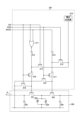
- FIG. 7 is a circuit diagram showing an example of the configuration of an oscillator circuit according to the fourth embodiment.
- this oscillator circuit has a current feedback section 252 instead of the current feedback section 202 of the third embodiment described above.
- the rest of the configuration of the oscillator circuit of the fourth embodiment is the same as the configuration of the oscillator circuit of the third embodiment described above.
- the current feedback section 252 is the current feedback section 202 of the third embodiment described above to which a compensation resistor 224 has been added.
- the rest of the configuration of the current feedback section 252 is the same as the configuration of the current feedback section 202 of the third embodiment described above.
- the compensation resistor 224 has a different temperature characteristic from the reference resistor 212.
- the temperature characteristic of the compensation resistor 224 can be set so that the temperature characteristic of the reference resistor 212 is compensated for.
- the compensation resistor 224 is connected in series to the switched capacitor 206.
- the resistance value of the compensation resistor 224 is R'
- the resistance R when the switched capacitor 206 is regarded as an impedance is equal to Rr-R'
- the compensation resistor 224 which has a temperature characteristic different from that of the reference resistor 212, is connected in series to the switched capacitor 206.
- the switched capacitor 106 is provided in the FLL to generate the current Ic corresponding to the oscillation frequency fs of the oscillator 101.
- a bootstrap circuit used for switching the switched capacitor 106 is provided.
- FIG. 8 is a circuit diagram showing an example of the configuration of an oscillator circuit according to the fifth embodiment.
- this oscillator circuit has a switched capacitor 302 instead of the switched capacitor 106 of the first embodiment described above.
- this oscillator circuit has a bootstrap circuit 301 added to the oscillator circuit of the first embodiment described above.
- the rest of the configuration of the oscillator circuit of the fifth embodiment is the same as the configuration of the oscillator circuit of the first embodiment described above.
- the switched capacitor 302 generates a current Ic according to the oscillation frequency fs of the oscillator 101 based on a switching operation.
- the switched capacitor 302 includes transistors 321 and 322, capacitors 325 and 326, and variable capacitances 323 and 324.
- Transistors 321 and 322 are connected in series to each other, and variable capacitances 323 and 324 are connected in parallel to their connection point.
- Capacitors 325 and 326 are connected to both ends of the series circuit of transistors 321 and 322, respectively.
- N-channel field effect transistors may be used for transistors 321 and 322.
- the bootstrap circuit 301 drives the gates of the transistors 321 and 322. At this time, the bootstrap circuit 301 can boost the drive voltage of the transistors 321 and 322.
- the bootstrap circuit 301 includes a voltage generation source 310, a NOR circuit 311, capacitors 312 and 313, and transistors 314 to 319.
- the transistors 316 and 317 may be P-channel field effect transistors, and the transistors 314, 315, 318, and 319 may be N-channel field effect transistors.
- Transistor 316 is connected between the gate of transistor 321 and capacitor 312.
- Transistor 317 is connected between the gate of transistor 322 and capacitor 313.
- Transistor 318 is connected between the gate of transistor 321 and ground potential.
- Transistor 319 is connected between the gate of transistor 322 and ground potential.
- Transistor 314 is connected between the connection point of transistor 316 and capacitor 312 and voltage generation source 310.
- Transistor 315 is connected between the connection point of transistor 317 and capacitor 313 and voltage generation source 310.
- the output of NOR circuit 311 is connected to capacitor 312.
- the clock signal CK is input to the gates of each of the transistors 314, 316, and 318 and to the NOR circuit 311.
- the inverted clock signal XCK is input to the gates of each of the transistors 315, 317, and 319.
- the inverted clock signal XCK is an inverted signal of the clock signal CK.
- the non-overlap signal XXCK is input to the capacitor 313 and the NOR circuit 311.
- the non-overlap signal XXCK can provide a non-overlap period between the on period of the clock signal CK and the on period of the inverted clock signal XCK.
- transistor 314 turns on according to clock signal CK
- transistor 315 turns on according to inverted clock signal XCK.
- each of capacitors 312 and 313 is charged up via voltage generating source 310.
- transistors 316 and 318 are alternately turned on in accordance with the clock signal CK
- transistors 317 and 319 are alternately turned on in accordance with the inverted clock signal XCK.
- the gate of transistor 321 is alternately switched between connection to capacitor 312 and connection to ground potential in accordance with the clock signal CK.
- the gate of transistor 322 is alternately switched between connection to capacitor 313 and connection to ground potential in accordance with the inverted clock signal XCK.
- a current Ic is generated in the switched capacitor 302 and output to the cascode current mirror circuit 107 in FIG. 2.
- the drive voltage applied to the gates of each transistor 321 and 322 is boosted based on the charge accumulated in each capacitor 312 and 322, and the on-resistance of each transistor 321 and 322 is reduced.
- a bootstrap circuit 301 is provided to drive the switched capacitor 302. This makes it possible to reduce the on-resistance of the switched capacitor 302 during switching, and to improve the accuracy of the FLL frequency.
- the bias voltage may be any voltage, or the bias voltage may be referenced. Also, a bias voltage generated by a bootstrap replica circuit may be used.
- FIG. 9 is a circuit diagram showing an example of the configuration of an oscillator circuit according to the sixth embodiment.
- this oscillator circuit has a cascode current mirror circuit 407 instead of the cascode current mirror circuit 107 of the first embodiment described above.
- this oscillator circuit has a chopper circuit 411 added to the oscillator circuit of the first embodiment described above.
- the rest of the configuration of the oscillator circuit of the sixth embodiment is the same as the configuration of the oscillator circuit of the first embodiment described above.
- the cascode current mirror circuit 407 is obtained by adding a chopper circuit 412 to the cascode current mirror circuit 107 of the first embodiment described above.
- the rest of the configuration of the cascode current mirror circuit 407 of the sixth embodiment is the same as the configuration of the cascode current mirror circuit 407 of the first embodiment described above.
- Each chopper circuit 411, 412 alternately switches the output destination of the current Ic generated by the switched capacitor 106 and the output destination of the reference current Ir. At this time, the chopper circuit 411 alternately switches these output destinations on the input side of the cascode current mirror circuit 407. The chopper circuit 412 alternately switches these output destinations on the output side of the cascode current mirror circuit 407.
- the input terminal AP of the chopper circuit 411 is connected to the reference resistor 112, and the input terminal AN of the chopper circuit 411 is connected to the switched capacitor 106.
- the output terminal BP of the chopper circuit 411 is connected to the connection point of the mirror transistors 125 and 127, and the output terminal BN of the chopper circuit 411 is connected to the connection point of the mirror transistors 126 and 128.
- the input terminal AP of the chopper circuit 412 is connected to the connection point of the mirror transistors 123 and 125, and the input terminal AN of the chopper circuit 412 is connected to the connection point of the mirror transistors 124 and 126.
- the output terminal BP of the chopper circuit 412 is connected to the gates of the mirror transistors 127 and 128, and the output terminal BN of the chopper circuit 412 is connected to the loop filter 103.
- FIG. 10 is a circuit diagram showing a first example of a chopper circuit according to the sixth embodiment.
- the chopper circuit includes transistors 421 to 424.
- Each of the transistors 421 to 424 may be an N-channel field effect transistor.
- the transistor 421 is connected between the input terminal AP and the output terminal BP of the chopper circuit.
- the transistor 422 is connected between the input terminal AP and the output terminal BN of the chopper circuit.
- the transistor 423 is connected between the input terminal AN and the output terminal BP of the chopper circuit.
- the transistor 424 is connected between the input terminal AN and the output terminal BN of the chopper circuit.
- a chopper signal CP is applied to the gates of the transistors 421 and 424, and an inverted chopper signal CPB is applied to the gates of the transistors 422 and 423.
- the inverted chopper signal CPB is an inverted version of the chopper signal CP.
- the chopper signal CP may be generated by dividing the frequency of the FLL output.
- FIG. 11 is a circuit diagram showing a second example of a chopper circuit according to the sixth embodiment.
- the chopper circuit includes transmission gates 431 to 434.
- Each of the transmission gates 431 to 434 can use a pair of an N-channel field effect transistor and a P-channel field effect transistor.
- the transmission gate 431 is connected between the input terminal AP and the output terminal BP of the chopper circuit.
- the transmission gate 432 is connected between the input terminal AP and the output terminal BN of the chopper circuit.
- the transmission gate 433 is connected between the input terminal AN and the output terminal BP of the chopper circuit.
- the transmission gate 434 is connected between the input terminal AN and the output terminal BN of the chopper circuit.
- a chopper signal CP is applied to the non-inverting gate of each of the transmission gate transistors 431 and 434, and an inverted chopper signal CPB is applied to the inverting gate of each of the transmission gate transistors 431 and 434.
- a chopper signal CP is applied to the inverting gate of each of the transmission gate transistors 432 and 433, and an inverted chopper signal CPB is applied to the non-inverting gate of each of the transmission gate transistors 432 and 433.
- FIG. 12 is a timing chart showing the chopper operation of the oscillator circuit according to the sixth embodiment.
- the chopper signal CP can be generated, for example, by dividing the oscillation signal Sc of the oscillator 101 by 16. A non-overlapping period can be provided between the chopper signal CP and the inverted chopper signal CPB.
- each chopper circuit 411, 412 When the chopper signal CP is turned on, the input terminal AP and output terminal BP of each chopper circuit 411, 412 are connected, and the input terminal AN and output terminal BN of each chopper circuit 411, 412 are connected.
- the inverted chopper signal CPB When the inverted chopper signal CPB is turned on, the input terminal AP and output terminal BN of each chopper circuit 411, 412 are connected, and the input terminal AN and output terminal BP of each chopper circuit 411, 412 are connected.
- the current Ic generated by the switched capacitor 106 and the reference current Ir generated by the reference resistor 112 flow alternately through the mirror transistors 127, 128, and the current Ic generated by the switched capacitor 106 and the reference resistor 112 can be evenly passed through each mirror transistor 127, 128.
- chopper circuits 411, 412 are provided that alternately switch the output destination of the current Ic generated by the switched capacitor 106 and the output destination of the reference current Ir. This makes it possible to prevent mismatching of the current mirror for comparing the current Ic generated by the switched capacitor 106 with the reference current Ir generated by the reference resistor 112, and to improve the accuracy of the FLL frequency.
- the oscillation frequency of the FLL is controlled based on current feedback.
- an FLL whose oscillation frequency is controlled based on current feedback is applied to a solid-state imaging device.
- FIG. 13 is a block diagram showing an example of the configuration of a solid-state imaging device to which an oscillator circuit according to the seventh embodiment is applied. Note that in this figure, blocks that operate based on a clock signal are selected from among the blocks used in the solid-state imaging device 501.
- the solid-state imaging device 501 includes an FLL 502, frequency divider circuits 503 and 505, an AD converter 504, a logic circuit 506, and a communication interface 507.
- the FLL 502 can be used as a clock source for the AD converter 504, the logic circuit 506, and the communication interface 507.
- the clock frequency of the FLL 502 can be set according to the operating frequency of the communication interface 507.
- frequency divider circuits 503 and 505 may be provided in front of the AD converter 504 and logic circuit 506, respectively, according to the operating frequencies of the AD converter 504 and logic circuit 506.
- the FLL 502 whose oscillation frequency is controlled based on current feedback, is applied to the solid-state imaging device 501.
- This makes it possible to increase the frequency of the clock signal used in the solid-state imaging device 501 while suppressing an increase in the power consumption of the oscillator circuit, thereby enabling higher resolution and higher frame rates to be achieved while suppressing an increase in the power consumption of the solid-state imaging device 501.
- the FLL 502 may be adapted to operate at a higher frequency in response to an increase in the speed of the AD converter 504.
- the bootstrap circuit 301 of the fifth embodiment described above may be applied to the FLL 502.
- the FLL 502 whose oscillation frequency is controlled based on current feedback, is applied to the solid-state imaging device 501.
- a PLL used in the AD converter 504 and logic circuit 506, and a PLL used in the communication interface 507 are provided in a stage subsequent to the FLL 502.
- FIG. 14 is a block diagram showing an example of the configuration of a solid-state imaging device to which an oscillator circuit according to the eighth embodiment is applied.
- solid-state imaging device 511 is obtained by adding PLLs 512 and 513 to solid-state imaging device 501 of the seventh embodiment described above.
- the rest of the configuration of solid-state imaging device 511 of the eighth embodiment is the same as the configuration of solid-state imaging device 501 of the seventh embodiment described above.
- PLL 512 is connected before the frequency divider circuits 503 and 505.
- PLL 513 is connected before the communication interface 507.
- the output of FLL 502 is input to frequency divider circuits 503 and 505 via PLL 512, and is divided by frequency divider circuits 503 and 505 before being input to AD converter 504 and logic circuit 506.
- the output of FLL 502 is input to communication interface 507 via PLL 513.
- PLLs 512 and 513 are connected after FLL 502, whose oscillation frequency is controlled based on current feedback. This makes it possible to increase the frequency of the clock signal used in solid-state imaging device 501 while stabilizing and improving the accuracy of the clock signal frequency.
- the PLL 512 used in the AD converter 504 and the logic circuit 506, and the PLL 513 used in the communication interface 507 are provided in the subsequent stage of the FLL 502.
- the PLL 512 used in the AD converter 504 and the logic circuit 506 is provided in the subsequent stage of the FLL 502.
- FIG. 15 is a block diagram showing an example of the configuration of a solid-state imaging device to which an oscillator circuit according to the ninth embodiment is applied.
- solid-state imaging device 521 is obtained by adding a PLL 512 to solid-state imaging device 501 of the seventh embodiment described above.
- the rest of the configuration of solid-state imaging device 521 of the ninth embodiment is the same as the configuration of solid-state imaging device 501 of the seventh embodiment described above.
- the PLL 512 is connected before the frequency divider circuits 503 and 505. At this time, the output of the PLL 502 is input to the frequency divider circuits 503 and 505 via the PLL 512, and is divided by the frequency divider circuits 503 and 505 before being input to the AD converter 504 and the logic circuit 506.
- the PLL 512 used in the AD converter 504 and logic circuit 506 is provided after the FLL 502. This makes it possible to increase the frequency of the clock signal used in the AD converter 504 and logic circuit 506 while stabilizing the frequency of the clock signal and improving its accuracy.
- the PLL 512 used in the AD converter 504 and the logic circuit 506 is provided after the FLL 502.
- the PLL 513 used in the communication interface 507 is provided after the FLL 502.
- FIG. 16 is a block diagram showing an example of the configuration of a solid-state imaging device to which an oscillator circuit according to the tenth embodiment is applied.
- solid-state imaging device 531 is obtained by adding PLL 513 to solid-state imaging device 501 of the seventh embodiment described above.
- the rest of the configuration of solid-state imaging device 531 of the tenth embodiment is the same as the configuration of solid-state imaging device 501 of the seventh embodiment described above.
- PLL513 is connected in front of the communication interface 507. At this time, the output of PLL502 is input to the communication interface 507 via PLL513.
- the PLL 513 used in the communication interface 507 is provided after the FLL 502. This makes it possible to increase the frequency of the clock signal used in the communication interface 507 while stabilizing the frequency of the clock signal and improving its accuracy.
- the PLL 512 used in the AD converter 504 and the logic circuit 506, and the PLL 513 used in the communication interface 507 are provided after the FLL 502.
- the PLL 514 used in the AD converter 504, the logic circuit 506, and the communication interface 507 is provided after the FLL 502.
- FIG. 17 is a block diagram showing an example of the configuration of a solid-state imaging device to which an oscillator circuit according to the eleventh embodiment is applied.
- solid-state imaging device 541 is obtained by adding a PLL 514 to solid-state imaging device 501 of the seventh embodiment described above.
- the rest of the configuration of solid-state imaging device 541 of the eleventh embodiment is the same as the configuration of solid-state imaging device 501 of the seventh embodiment described above.
- PLL514 is connected after FLL502.
- the output of FLL502 is input to frequency divider circuits 503 and 505 via PLL514, and is input to AD converter 504 and logic circuit 506 after being divided by frequency divider circuits 503 and 505.
- the output of FLL502 is input to communication interface 507 via PLL514.
- the PLL 514 used in the AD converter 504, logic circuit 506, and communication interface 507 is provided after the FLL 502. This makes it possible to increase the frequency of the clock signal used in the AD converter 504, logic circuit 506, and communication interface 507 while stabilizing the frequency of the clock signal and improving its accuracy.
- the FLL 502 whose oscillation frequency is controlled based on current feedback, is applied to the solid-state imaging device 501.
- an FLL is used for the AD converter 504 and the logic circuit 506, and an FLL is used for the communication interface 507.
- FIG. 18 is a block diagram showing an example of the configuration of a solid-state imaging device to which an oscillator circuit according to the twelfth embodiment is applied.
- solid-state imaging device 551 includes FLLs 552 and 553 instead of FLL 502 of the seventh embodiment described above.
- the rest of the configuration of solid-state imaging device 551 of the twelfth embodiment is the same as the configuration of solid-state imaging device 501 of the first embodiment described above.
- the FLL 552 can be used as a clock source for the AD converter 504 and the logic circuit 506.
- the FLL 553 can be used as a clock source for the communication interface 507.
- the clock frequency of the FLL 553 can be set according to the operating frequency of the communication interface 507.
- frequency divider circuits 503 and 505 may be provided in front of the AD converter 504 and logic circuit 506, respectively, according to the operating frequencies of the AD converter 504 and logic circuit 506.
- the FLL 502 whose oscillation frequency is controlled based on current feedback, is applied to the solid-state imaging device 501.
- the frequency of the FLL 502 used in the solid-state imaging device is made externally controllable.
- FIG. 19 is a block diagram showing an example of the configuration of a solid-state imaging device to which an oscillator circuit according to the thirteenth embodiment is applied.
- solid-state imaging device 561 is obtained by adding logic circuit 562 to solid-state imaging device 501 of the seventh embodiment described above.
- the rest of the configuration of solid-state imaging device 561 of the thirteenth embodiment is the same as the configuration of solid-state imaging device 501 of the seventh embodiment described above.
- the solid-state imaging device 561 is connected to the processor 563.
- the processor 563 can receive frequency information FIM of the FLL 502. The processor 563 can then transmit to the solid-state imaging device 561 frequency adjustment information FID that adjusts the frequency of the FLL 502 in accordance with the deviation in the frequency of the FLL 502.
- the processor 563 may be a CPU (Central Processing Unit) or a GPU (Graphics Processing Unit).
- the processor 563 may be a single-core processor or a multi-core processor.
- the logic circuit 562 can adjust the frequency of the FLL 502 based on the frequency adjustment information FID transmitted from the processor 563.
- a variable capacitance element may be provided in the FLL 502.
- the logic circuit 562 can adjust the frequency of the FLL 502 by changing the capacitance of the variable capacitance element of the FLL 502 based on the frequency adjustment information FID.
- the frequency of the FLL 502 used in the solid-state imaging device 561 can be adjusted from the processor 563. This makes it possible to improve the accuracy of the frequency of the clock signal used in the solid-state imaging device 561.
- the oscillation frequency of the FLL is controlled based on current feedback.
- an FLL is used as a source oscillation circuit of the PLL, and the frequency of the PLL can be corrected based on a detection value related to the oscillation frequency of the FLL.
- FIG. 20 is a circuit diagram showing an example of the configuration of an oscillator circuit according to the fourteenth embodiment.
- the oscillator circuit includes an FLL 601, a frequency divider circuit 621, an ADPLL (All Digital PLL) 611, a temperature sensor 631, a detection data input unit 641, and a parameter correction unit 651.
- FLL 601 a frequency divider circuit 621
- ADPLL All Digital PLL
- the FLL 601 forms a synchronous loop based on the oscillation frequency. This synchronous loop may use current feedback or voltage feedback. For current feedback, any of the first to sixth embodiments described above may be used.
- the FLL 601 includes an oscillator 602 and a frequency synchronization unit 603.
- the oscillator 602 generates an oscillation signal Sc based on an oscillation operation.
- the oscillator 602 can change the oscillation frequency fs based on voltage control.
- the oscillator 602 may be a ring oscillator or an LC oscillator.
- the frequency synchronization unit 603 forms a feedback loop for the oscillator 602 based on the oscillation frequency fs of the oscillator 602.
- the frequency synchronization unit 603 in a synchronization loop using current feedback, can include a frequency-current conversion unit that converts the oscillation frequency fs of the oscillator 602 into a current.
- the frequency synchronization unit 603 in a synchronization loop using voltage feedback, can include a frequency-voltage conversion unit that converts the oscillation frequency fs of the oscillator 602 into a voltage.
- the frequency divider circuit 621 divides the output of the FLL 601 and inputs it to the ADPLL 611.
- the ADPLL 611 forms a feedback loop based on phase synchronization and outputs a clock signal CLK.
- the FLL 601 can be used as the source oscillator circuit of the ADPLL 611.
- the clock signal CLK can be determined based on the oscillation signal Sc and a FCW (Frequency Command Word) parameter.
- the FCW parameter can specify the ratio of the frequency of the clock signal CLK to the frequency of the oscillation signal Sc.
- the FCW parameter can be provided from outside the ADPLL 611.
- the ADPLL 611 includes an oscillator 612, a counter 613, a TDC (Time to Digital Converter) 614, an accumulator 615, an adder 616, and a loop filter 617.
- TDC Time to Digital Converter
- the oscillator 612 generates a clock signal CLK based on an oscillation operation.
- the oscillator 612 can change the oscillation frequency based on an oscillator tuning word.
- the oscillator 612 may be a ring oscillator or an LC oscillator.
- the counter 613 counts up for each clock of the clock signal CLK and outputs the count to the adder 616. At this time, the counter 613 can detect the phase in units of one cycle of the clock signal CLK.
- TDC 614 detects the phase of the clock signal CLK for less than one period and outputs it to adder 616.
- the accumulator 615 sets a count-up value for each period of the oscillation signal Sc based on the FCW parameter, and outputs the count-up value to the adder 616. At this time, the FCW parameter corrected by the parameter correction unit 651 is input to the accumulator 615.
- the adder 616 subtracts the output of the counter 613 and the output of the TDC 614 from the output of the accumulator 615 and outputs the result to the loop filter 617.
- the output of the adder 616 can indicate the phase error between the oscillation signal Sc and the clock signal CLK.
- the loop filter 617 band-limits the input to the oscillator 612, reducing the effects of quantization errors.
- the temperature sensor 631 detects the temperature of the oscillator circuit and outputs the detection result to the detection data input unit 641.
- the detection data input unit 641 inputs detection data related to the state of the FLL 601 to the parameter correction unit 651.
- the state of the FLL 601 may include the power supply voltage VDD supplied to the FLL 601, the temperature of the FLL 601, and the control voltage VCT of the oscillator 602.
- the temperature of the FLL 601 can be detected by the temperature sensor 631.
- the detection data input unit 641 includes switches 642 to 644, an AD converter 645, and a selector 646.
- the switches 642 to 644 may be field effect transistors.
- Switch 642 inputs the power supply voltage VDD to AD converter 645 based on the timing specified by the control signal CNT.
- Switch 643 inputs the control voltage VCT to AD converter 645 based on the timing specified by the control signal CNT.
- Switch 644 inputs the detection value of temperature sensor 631 to AD converter 645 based on the timing specified by the control signal CNT.
- the AD converter 645 converts the power supply voltage VDD, the control voltage VCT, and the detection value of the temperature sensor 631 into digital form and inputs them to the selector 646.
- the selector 646 switches the output destination of the AD converter 645 based on the timing specified by the control signal CNT. At this time, the selector 646 inputs the AD converted value of the power supply voltage VDD to the power supply voltage correction value calculation unit 652, inputs the AD converted value of the control voltage VCT to the control voltage correction value calculation unit 653, and inputs the AD converted value of the detection value of the temperature sensor 631 to the temperature correction value calculation unit 654.
- the parameter correction unit 651 corrects the FCW parameters based on the power supply voltage VDD, the control voltage VCT, and the detection value of the temperature sensor 631.
- the parameter correction unit 651 includes a power supply voltage correction value calculation unit 652, a control voltage correction value calculation unit 653, a temperature correction value calculation unit 654, a correction coefficient storage unit 655, and multipliers 656 to 658.
- the power supply voltage correction value calculation unit 652 calculates a correction value for the power supply voltage VDD based on the monitor voltage V of the power supply voltage VDD. For example, if the reference value of the monitor voltage V is V0 and the correction coefficients are ⁇ 1 , ⁇ 2 , ⁇ 3 , ..., the correction value of the power supply voltage VDD can be given by the following formula. 1+ ⁇ 1 (V-V 0 )+ ⁇ 2 (V-V 0 ) 2 + ⁇ 3 (V-V 0 ) 3 +...
- the control voltage correction value calculation unit 653 calculates a correction value for the control voltage VCT based on the monitor voltage C of the control voltage VCT. For example, if the reference value of the monitor voltage C is C0 and the correction coefficients are ⁇ 1 , ⁇ 2 , ⁇ 3 , ..., the correction value for the control voltage VCT can be given by the following formula. 1+ ⁇ 1 (C-C 0 )+ ⁇ 2 (C-C 0 ) 2 + ⁇ 3 (C-C 0 ) 3 +...
- the temperature correction value calculation unit 654 calculates the temperature correction value based on the detection value T of the temperature sensor 631. For example, if the reference value of the detection value T of the temperature sensor 631 is T 0 and the correction coefficients are ⁇ 1 , ⁇ 2 , ⁇ 3 , ..., the temperature correction value can be given by the following formula. 1+ ⁇ 1 (T-T 0 )+ ⁇ 2 (T-T 0 ) 2 + ⁇ 3 (T-T 0 ) 3 +...
- the correction coefficient storage unit 655 stores the reference values V 0 , C 0 , T 0 and the correction coefficients ⁇ 1 , ⁇ 2 , ⁇ 3 , . . . , ⁇ 1 , ⁇ 2 , ⁇ 3 , . . . , ⁇ 1 , ⁇ 2 , ⁇ 3 , . . . , ⁇ 1 , ⁇ 2 , ⁇ 3 , . . . .
- the correction coefficients ⁇ 1 , ⁇ 2 , ⁇ 3 , ... can be set to have the inverse characteristic of the frequency fluctuation with respect to the fluctuation of the power supply voltage VDD.
- the correction coefficients ⁇ 1 , ⁇ 2 , ⁇ 3 , ... can be set to have the inverse characteristic of the frequency fluctuation with respect to the fluctuation of the control voltage VCT.
- the correction coefficients ⁇ 1 , ⁇ 2 , ⁇ 3 , ... can be set to have the inverse characteristic of the frequency fluctuation with respect to the fluctuation of the temperature.
- Multiplier 656 multiplies the FCW parameter by the correction value calculated by temperature correction value calculation unit 654 and outputs the result to multiplier 657.
- Multiplier 657 multiplies the correction value calculated by control voltage correction value calculation unit 653 by the output of multiplier 656 and outputs the result to multiplier 658.
- the multiplier 658 multiplies the correction value calculated by the power supply voltage correction value calculation unit 652 by the output FCW parameter of the multiplier 657 and outputs the result to the accumulator 615.
- Figure 21 is a diagram showing the relationship between the operating environment and the oscillation frequency of the oscillator circuit according to the fourteenth embodiment.
- a shows the relationship between the detection value of the temperature sensor 631, the power supply voltage VDD, and the frequency of the oscillation signal Sc for the oscillation signal Sc of the oscillator 602 when there is no frequency synchronization unit 603.
- b shows the relationship between the detection value of the temperature sensor 631, the power supply voltage VDD, the control voltage VCT, and the frequency of the oscillation signal Sc for the oscillation signal Sc of the FLL 601.
- c shows the relationship between the detection value of the temperature sensor 631, the power supply voltage VDD, the control voltage VCT, and the frequency of the clock signal CLK for the clock signal CLK of the ADPLL 611.
- the frequency of the oscillation signal Sc of the oscillator 602 fluctuates greatly in accordance with fluctuations in the ambient temperature of the oscillator 602 and the power supply voltage VDD.
- the oscillation signal Sc of the FLL 601 is suppressed in frequency fluctuation in response to fluctuations in the ambient temperature of the FLL 601 and in the power supply voltage VDD.
- the frequency of the clock signal CLK of the ADPLL 611 is maintained almost constant despite fluctuations in the ambient temperature of the FLL 601, the power supply voltage VDD, and the control voltage VCT.
- the FLL 601 is used as the source oscillator circuit of the ADPLL 611, and the clock frequency of the ADPLL 611 can be corrected based on a detection value related to the oscillation frequency fs of the FLL 601. This makes it possible to stabilize the clock frequency of the clock signal CLK while responding to fluctuations in the operating environment of the oscillator circuit.
- the range of the correction amount by the parameter correction unit 651 can be made smaller than when the oscillator 602 is used as the source oscillator circuit of the ADPLL 611, and the clock frequency of the ADPLL 611 can be stabilized.
- the FLL 601 is used as the source oscillation circuit of the ADPLL 611, and the clock frequency of the ADPLL 611 can be corrected based on a detection value related to the oscillation frequency fs of the FLL 601.
- an LC oscillator is used for the oscillator 602 of the FLL 601 used as the source oscillation circuit of the ADPLL 611.
- FIG. 22 is a circuit diagram showing an example of the configuration of an oscillator circuit according to the fifteenth embodiment.
- the oscillator 602 includes an LC oscillator 702.
- the LC oscillator 702 is obtained by adding varactors 751 and 752 to the LC oscillator in FIG. 4.
- the gate capacitance of a field effect transistor can be used as the variable capacitance of each of the varactors 751 and 752.
- the varactor 751 is connected between the low-pass filter 714 and one end of the capacitor 142
- the varactor 752 is connected between the low-pass filter 714 and the other end of the capacitor 142.
- a power supply voltage VDD may be applied to the center tap of the inductor 141.
- the frequency synchronization unit 603 includes a frequency-voltage conversion unit 701 and a frequency division circuit 703.
- the frequency-voltage conversion unit 701 generates a control voltage VCT that corresponds to the oscillation frequency fs of the LC oscillator 702.
- the frequency-voltage conversion unit 701 includes a switched capacitor 712, an amplifier 713, and a low-pass filter 714.
- the amplifier 713 is connected to the rear of the switched capacitor 712
- the low-pass filter 714 is connected to the rear of the amplifier 713
- the LC oscillator 702 is connected to the rear of the low-pass filter 714.
- the switched capacitor 712 generates a voltage Vs according to the oscillation frequency fs of the LC oscillator 702 based on a switching operation.
- the switched capacitor 712 includes transistors 721 and 722, a resistor 724, and capacitors 723 and 725.
- the transistors 721 and 722 may be P-channel field effect transistors.
- Transistors 721 and 722 are connected in series with each other, and a capacitor 723 is connected to their connection point. Each of transistors 721 and 722 is switched based on the output of frequency divider circuit 703. Resistor 724 and capacitor 725 are connected in parallel with each other, and the parallel circuit is connected between transistor 722 and ground potential.
- each of the transistors 721, 722 and the capacitor 723 can be regarded as the impedance of the resistor R, and a voltage Vs corresponding to the oscillation frequency fs of the LC oscillator 702 is generated as the divided voltage of the resistor R and resistor 724 determined by each of the transistors 721, 722 and the capacitor 723.
- Amplifier 713 includes differential amplifier 731 and resistors 732 and 733. Resistors 732 and 733 are connected in series with each other, and one input terminal of differential amplifier 731 is connected to the connection point between them. At this time, resistors 732 and 733 can generate a reference voltage Vr and input it to one input terminal of differential amplifier 731. Low-pass filter 714 is connected to the output terminal of amplifier 713.
- differential amplifier 731 compares voltage Vs generated by switched capacitor 712 with reference voltage Vr, and outputs the difference between them to low-pass filter 714.
- Low-pass filter 714 extracts the low-frequency components of the output of amplifier 713 and outputs it as a control voltage VCT for LC oscillator 702.
- Low-pass filter 714 includes resistor 741 and capacitor 742. Resistor 741 is connected between low-pass filter 714 and LC oscillator 702. Capacitor 742 is connected between the connection point of resistor 741 and LC oscillator 702 and ground potential. Low-pass filter 714 also inputs control voltage VCT to switch 643 via buffer 705.
- the frequency divider circuit 703 divides the output of the LC oscillator 702 and inputs it to the switched capacitor 712. In this case, the frequency divider circuit 703 can have two feedback loops according to the differential output of the LC oscillator 702.
- Figure 23 is a diagram showing the state of each part during operation of the oscillator circuit according to the fifteenth embodiment.
- a in the figure shows the relationship between the oscillation frequency fs/N of the LC oscillator 702 when divided by N by the frequency divider circuit 703 and the voltage Vs generated by the switched capacitor 712.
- b in the figure shows the relationship between the control voltage VCT output from the frequency voltage converter 701 and time t.
- c in the figure shows the relationship between the control voltage VCT output from the frequency voltage converter 701 and the oscillation frequency fs of the LC oscillator 702.
- d in the figure shows the relationship between the waveform (amplitude V) of the oscillation signal of the LC oscillator 702 and time t.
- e in the figure shows the relationship between the oscillation frequency fs of the LC oscillator 702 and time t.
- Differential amplifier 731 generates a differential voltage between voltage Vs generated by switched capacitor 712 and reference voltage Vr, and outputs it to low-pass filter 714.
- Low-pass filter 714 extracts the low-frequency components of the output of differential amplifier 731 to generate control voltage VCT, which is output to LC oscillator 702.
- control voltage VCT is applied to varactors 751 and 752.
- the capacitance of varactors 751 and 752 is changed based on control voltage VCT, and the oscillation frequency fs of LC oscillator 702 changes.
- Vs0 is not equal to Vr, so the DC signal obtained by amplifying the difference voltage moves in the direction of lowering VCT.
- Fs increases, approaching f1, and the frequency divider circuit approaches f1/N.
- fs/N increases, the switched capacitor operates to approach Vs1.
- Vs0 and Vr become equal, VCT becomes Vc1 and stabilizes, and as a result, fs also stabilizes at f1.
- the LC oscillator 702 is frequency-synchronized as the source oscillation circuit of the ADPLL 611 to provide a stable fs, and the clock frequency of the ADPLL 611 can be corrected based on a detection value related to the oscillation frequency fs of the FLL 601. This makes it possible to stabilize the clock frequency of the clock signal CLK against variations in the characteristics of the LC oscillator 702, while also contributing to stabilizing the clock frequency of the clock signal CLK against variations in the operation of the frequency-to-voltage conversion unit 701.
- ADPLL611 can be operated as a high-pass filter based on the loop characteristics of ADPLL611. This makes it possible to suppress the effects of low-frequency flicker noise generated by FLL601, and to suppress deterioration of the frequency accuracy of the clock signal CLK.
- the temperature characteristics can be suppressed even when a low-Q inductor is used for the LC oscillator702.
- control voltage correction value calculation unit 653 it is possible to suppress deterioration in the frequency accuracy of the clock signal CLK even when the control voltage VCT exceeds the adjustment range.
- a power supply voltage correction value calculation unit 652 and a temperature correction value calculation unit 654 are provided. This makes it possible to suppress deterioration in the frequency accuracy of the clock signal CLK even when the power supply voltage and ambient temperature of the FLL 601 fluctuate and the operation of the switched capacitor 712 and amplifier 713 varies.
- an LC oscillator is used for the oscillator 602 of the FLL 601 used as the source oscillation circuit of the ADPLL 611.
- a ring oscillator is used for the oscillator 602 of the FLL 601 used as the source oscillation circuit of the ADPLL 611.
- FIG. 24 is a circuit diagram showing an example of the configuration of an oscillator circuit according to the sixteenth embodiment.
- this oscillator circuit includes a ring oscillator 802, a transistor 803, and a buffer 804 instead of the LC oscillator 702 of the fifteenth embodiment described above.
- the rest of the configuration of the oscillator circuit of the sixteenth embodiment is the same as that of the oscillator circuit of the fifteenth embodiment described above.
- the ring oscillator 802 can be configured similarly to the ring oscillator in FIG. 3.
- the ring oscillator 802 is connected to the divider circuit 704 via a buffer 804.
- Transistor 803 controls the tail current of each inverter 131 used in ring oscillator 802.
- An N-channel field effect transistor can be used as transistor 803.
- Transistor 803 is connected between the low-voltage power supply terminal of each inverter 131 and ground potential.
- a control voltage VCT is input to the gate of transistor 803. At this time, control voltage VCT adjusts the current flowing through transistor 803, and can adjust the oscillation frequency of ring oscillator 802.
- the ring oscillator 802 is frequency-synchronized as the source oscillation circuit of the ADPLL 611 to provide a stable fs, and the clock frequency of the ADPLL 611 can be corrected based on a detection value related to the oscillation frequency fs of the FLL 801. This makes it possible to stabilize the clock frequency of the clock signal CLK against variations in the characteristics of the ring oscillator 802, while also contributing to stabilizing the clock frequency of the clock signal CLK against variations in the operation of the frequency-to-voltage conversion unit 701.
- the FLL 601 is used as the source oscillation circuit of the ADPLL 611, and the clock frequency of the ADPLL 611 can be corrected based on a detection value related to the oscillation frequency fs of the FLL 601.
- an LC oscillator is used as the source oscillation circuit of the ADPLL 611, and the frequency of the ADPLL 611 can be corrected based on a detection value related to the oscillation frequency of the LC oscillator.
- FIG. 25 is a circuit diagram showing an example of the configuration of an oscillator circuit according to the seventeenth embodiment.
- this oscillator circuit includes an LC oscillator 902 and a frequency-voltage converter 901 instead of the frequency-voltage converter 701 of the fifteenth embodiment described above.
- the rest of the configuration of the oscillator circuit of the seventeenth embodiment is the same as the configuration of the oscillator circuit of the fifteenth embodiment described above.
- the LC oscillator 902 is the same as the LC oscillator 702 of the fifteenth embodiment described above except that the varactors 751 and 752 have been removed.
- the rest of the configuration of the LC oscillator 902 of the seventeenth embodiment is the same as the configuration of the LC oscillator 702 of the fifteenth embodiment described above.
- the frequency-voltage conversion unit 901 includes an amplifier 913 instead of the amplifier 713 of the fifteenth embodiment described above.
- the rest of the configuration of the frequency-voltage conversion unit 901 of the seventeenth embodiment is the same as the configuration of the frequency-voltage conversion unit 701 of the fifteenth embodiment described above.
- a switched capacitor 712 is connected in front of the amplifier 913, and a low-pass filter 714 is connected in the rear of the amplifier 913.
- the LC oscillator 702 is connected in the rear of the low-pass filter 714, but in this 17th embodiment, the LC oscillator 702 is not connected in the rear of the low-pass filter 714. Therefore, in the above-mentioned 15th embodiment, the FLL 601 is used as the source oscillation circuit of the ADPLL 611, but in this 17th embodiment, the LC oscillator 902 is used as the source oscillation circuit of the ADPLL 611.
- the amplifier 913 includes a voltage follower circuit 914.
- the voltage Vs generated by the switched capacitor 712 is input to the low-pass filter 714 via the voltage follower circuit 914.
- the LC oscillator 902 is used as the source oscillation circuit of the ADPLL 611, and the frequency of the ADPLL 611 can be corrected based on a detection value related to the oscillation frequency of the LC oscillator 902. This makes it possible to stabilize the clock frequency of the clock signal CLK using the LC oscillator 902 as the source oscillation circuit of the ADPLL 611 while responding to fluctuations in the operating environment of the oscillation circuit.
- the LC oscillator 902 is used as the source oscillation circuit of the ADPLL 611, and the frequency of the ADPLL 611 can be corrected based on a detection value related to the oscillation frequency of the LC oscillator 902.
- a ring oscillator 802 may be used as the source oscillation circuit of the ADPLL 611 instead of the LC oscillator 902.
- the oscillation frequency of the FLL is controlled based on current feedback.
- substrates on which a solid-state imaging device having a pixel array section in which pixels are arranged in a matrix are formed are laminated.
- FIG. 26 is a perspective view showing an example of a stack of a solid-state imaging device according to the 18th embodiment.
- the solid-state imaging device includes semiconductor substrates 921 and 922.
- Semiconductor substrate 922 is stacked on semiconductor substrate 921.
- the material of semiconductor substrates 921 and 922 may be Si, InGaAs, or InP.
- a pixel array section 923 is formed on the semiconductor substrate 922.
- pixels 931 are arranged in a matrix in the row and column directions.
- Pad electrodes 932 and via electrodes 933 are formed around the periphery of the pixel array section 923.
- the via electrodes 933 penetrate the semiconductor substrate 922 and can electrically connect the semiconductor substrates 921 and 922 to each other.
- a peripheral circuit 924 is formed on the semiconductor substrate 921.
- a column readout circuit 925, a column ADC 926, a communication interface 927, and an oscillation circuit 928 are formed in the peripheral circuit 924.
- the column readout circuit 925 and the column ADC 926 may be formed to correspond to positions on both sides of the pixel array section 923 in the column direction.
- the oscillation circuit 928 may use any of the configurations of the first to seventeenth embodiments described above.
- the semiconductor substrate 922 on which the pixel array section 923 is formed is stacked on the semiconductor substrate 921 on which the peripheral circuit 924 is formed. This makes it possible to increase the sensitivity of the solid-state imaging device while suppressing an increase in the mounting area of the semiconductor chip on which the solid-state imaging device is formed.
- the oscillator circuit was applied to a solid-state imaging device, but the oscillator circuit can be applied to any circuit, such as an integrated circuit, as long as it operates based on a clock signal.
- the oscillator circuit may be used as a reference clock source for the integrated circuit.
- the oscillator circuit may be used as a reference clock source for a processor, a communication device, an AD converter, a logic circuit, an image processing circuit, a display device, etc.
- the technology according to the present disclosure can be applied to various products.
- the technology according to the present disclosure may be realized as a device mounted on any type of moving body such as an automobile, an electric vehicle, a hybrid electric vehicle, a motorcycle, a bicycle, a personal mobility device, an airplane, a drone, a ship, or a robot.
- FIG. 27 is a block diagram showing a schematic configuration example of a vehicle control system, which is an example of a mobile object control system to which the technology disclosed herein can be applied.
- the vehicle control system 12000 includes a plurality of electronic control units connected via a communication network 12001.
- the vehicle control system 12000 includes a drive system control unit 12010, a body system control unit 12020, an outside vehicle information detection unit 12030, an inside vehicle information detection unit 12040, and an integrated control unit 12050.
- Also shown as functional components of the integrated control unit 12050 are a microcomputer 12051, an audio/video output unit 12052, and an in-vehicle network I/F (interface) 12053.
- the drive system control unit 12010 controls the operation of devices related to the drive system of the vehicle according to various programs.
- the drive system control unit 12010 functions as a control device for a drive force generating device for generating the drive force of the vehicle, such as an internal combustion engine or a drive motor, a drive force transmission mechanism for transmitting the drive force to the wheels, a steering mechanism for adjusting the steering angle of the vehicle, and a braking device for generating a braking force for the vehicle.
- the body system control unit 12020 controls the operation of various devices installed in the vehicle body according to various programs.
- the body system control unit 12020 functions as a control device for a keyless entry system, a smart key system, a power window device, or various lamps such as headlamps, tail lamps, brake lamps, turn signals, and fog lamps.
- radio waves or signals from various switches transmitted from a portable device that replaces a key can be input to the body system control unit 12020.
- the body system control unit 12020 accepts the input of these radio waves or signals and controls the vehicle's door lock device, power window device, lamps, etc.
- the outside-vehicle information detection unit 12030 detects information outside the vehicle equipped with the vehicle control system 12000.
- the image capturing unit 12031 is connected to the outside-vehicle information detection unit 12030.
- the outside-vehicle information detection unit 12030 causes the image capturing unit 12031 to capture images outside the vehicle and receives the captured images.
- the outside-vehicle information detection unit 12030 may perform object detection processing or distance detection processing for people, cars, obstacles, signs, or characters on the road surface based on the received images.
- the imaging unit 12031 is an optical sensor that receives light and outputs an electrical signal according to the amount of light received.
- the imaging unit 12031 can output the electrical signal as an image, or as distance measurement information.
- the light received by the imaging unit 12031 may be visible light, or may be invisible light such as infrared light.
- the in-vehicle information detection unit 12040 detects information inside the vehicle.
- a driver state detection unit 12041 that detects the state of the driver is connected.
- the driver state detection unit 12041 includes, for example, a camera that captures an image of the driver, and the in-vehicle information detection unit 12040 may calculate the driver's degree of fatigue or concentration based on the detection information input from the driver state detection unit 12041, or may determine whether the driver is dozing off.
- the microcomputer 12051 can calculate control target values for the driving force generating device, steering mechanism, or braking device based on information inside and outside the vehicle acquired by the outside vehicle information detection unit 12030 or the inside vehicle information detection unit 12040, and output control commands to the drive system control unit 12010.
- the microcomputer 12051 can perform cooperative control aimed at realizing the functions of an Advanced Driver Assistance System (ADAS), including vehicle collision avoidance or impact mitigation, following driving based on the distance between vehicles, maintaining vehicle speed, vehicle collision warning, or vehicle lane departure warning.
- ADAS Advanced Driver Assistance System
- the microcomputer 12051 can also perform cooperative control for the purpose of autonomous driving, which allows the vehicle to travel autonomously without relying on the driver's operation, by controlling the driving force generating device, steering mechanism, braking device, etc. based on information about the surroundings of the vehicle acquired by the outside vehicle information detection unit 12030 or the inside vehicle information detection unit 12040.
- the microcomputer 12051 can also output control commands to the body system control unit 12020 based on information outside the vehicle acquired by the outside-vehicle information detection unit 12030. For example, the microcomputer 12051 can control the headlamps according to the position of a preceding vehicle or an oncoming vehicle detected by the outside-vehicle information detection unit 12030, and perform cooperative control aimed at preventing glare, such as switching high beams to low beams.
- the audio/image output unit 12052 transmits at least one output signal of audio and image to an output device capable of visually or audibly notifying the occupants of the vehicle or the outside of the vehicle of information.
- an audio speaker 12061, a display unit 12062, and an instrument panel 12063 are exemplified as output devices.
- the display unit 12062 may include, for example, at least one of an on-board display and a head-up display.
- FIG. 28 shows an example of the installation position of the imaging unit 12031.
- the imaging unit 12031 includes imaging units 12101, 12102, 12103, 12104, and 12105.
- the imaging units 12101, 12102, 12103, 12104, and 12105 are provided, for example, at the front nose, side mirrors, rear bumper, back door, and upper part of the windshield inside the vehicle cabin of the vehicle 12100.
- the imaging unit 12101 provided at the front nose and the imaging unit 12105 provided at the upper part of the windshield inside the vehicle cabin mainly acquire images of the front of the vehicle 12100.
- the imaging units 12102 and 12103 provided at the side mirrors mainly acquire images of the sides of the vehicle 12100.
- the imaging unit 12104 provided at the rear bumper or back door mainly acquires images of the rear of the vehicle 12100.
- the imaging unit 12105 provided at the upper part of the windshield inside the vehicle cabin is mainly used to detect leading vehicles, pedestrians, obstacles, traffic lights, traffic signs, lanes, etc.
- FIG. 28 shows an example of the imaging ranges of the imaging units 12101 to 12104.
- Imaging range 12111 indicates the imaging range of the imaging unit 12101 provided on the front nose
- imaging ranges 12112 and 12113 indicate the imaging ranges of the imaging units 12102 and 12103 provided on the side mirrors, respectively
- imaging range 12114 indicates the imaging range of the imaging unit 12104 provided on the rear bumper or back door.
- an overhead image of the vehicle 12100 viewed from above is obtained by superimposing the image data captured by the imaging units 12101 to 12104.
- At least one of the imaging units 12101 to 12104 may have a function of acquiring distance information.
- at least one of the imaging units 12101 to 12104 may be a stereo camera consisting of multiple imaging elements, or an imaging element having pixels for detecting phase differences.
- the microcomputer 12051 can obtain the distance to each solid object within the imaging ranges 12111 to 12114 and the change in this distance over time (relative speed with respect to the vehicle 12100) based on the distance information obtained from the imaging units 12101 to 12104, and can extract as a preceding vehicle, in particular, the closest solid object on the path of the vehicle 12100 that is traveling in approximately the same direction as the vehicle 12100 at a predetermined speed (e.g., 0 km/h or faster). Furthermore, the microcomputer 12051 can set the inter-vehicle distance that should be maintained in advance in front of the preceding vehicle, and perform automatic braking control (including follow-up stop control) and automatic acceleration control (including follow-up start control). In this way, cooperative control can be performed for the purpose of automatic driving, which runs autonomously without relying on the driver's operation.
- automatic braking control including follow-up stop control
- automatic acceleration control including follow-up start control
- the microcomputer 12051 classifies and extracts three-dimensional object data on three-dimensional objects, such as two-wheeled vehicles, ordinary vehicles, large vehicles, pedestrians, utility poles, and other three-dimensional objects, based on the distance information obtained from the imaging units 12101 to 12104, and can use the data to automatically avoid obstacles.
- the microcomputer 12051 distinguishes obstacles around the vehicle 12100 into obstacles that are visible to the driver of the vehicle 12100 and obstacles that are difficult to see.
- the microcomputer 12051 determines the collision risk, which indicates the risk of collision with each obstacle, and when the collision risk is equal to or exceeds a set value and there is a possibility of a collision, it can provide driving assistance for collision avoidance by outputting an alarm to the driver via the audio speaker 12061 or the display unit 12062, or by forcibly decelerating or steering to avoid a collision via the drive system control unit 12010.
- At least one of the imaging units 12101 to 12104 may be an infrared camera that detects infrared rays.
- the microcomputer 12051 can recognize a pedestrian by determining whether or not a pedestrian is present in the captured image of the imaging units 12101 to 12104. The recognition of such a pedestrian is performed, for example, by a procedure of extracting feature points in the captured image of the imaging units 12101 to 12104 as infrared cameras, and a procedure of performing pattern matching processing on a series of feature points that indicate the contour of an object to determine whether or not it is a pedestrian.
- the audio/image output unit 12052 controls the display unit 12062 to superimpose a rectangular contour line for emphasis on the recognized pedestrian.
- the audio/image output unit 12052 may also control the display unit 12062 to display an icon or the like indicating a pedestrian at a desired position.
- the technology disclosed herein can be applied to the microcomputer 12051, the in-vehicle network I/F 12053, the display unit 12062, the imaging unit 12031, and other components of the configuration described above.
- the above-mentioned oscillator circuit can be applied to the microcomputer 12051, the in-vehicle network I/F 12053, the display unit 12062, and the imaging unit 12031.
- the above-described embodiment shows an example for realizing the present technology, and there is a corresponding relationship between the matters in the embodiment and the matters specifying the invention in the claims. Similarly, there is a corresponding relationship between the matters specifying the invention in the claims and the matters in the embodiment of the present technology that have the same name.
- the present technology is not limited to the embodiment, and can be realized by making various modifications to the embodiment without departing from the gist of the technology.
- the effects described in this specification are merely examples and are not limiting, and other effects may also be present.
- the present technology can also be configured as follows. (1) an oscillator; a current feedback section that configures a feedback loop for the oscillator based on the current into which the oscillation frequency of the oscillator is converted. (2)
- the current feedback section is a frequency-current converter that converts an oscillation frequency of the oscillator into a current;
- the oscillation circuit according to (1) further comprising a differential current generating unit that generates a differential current between the current generated by the frequency-to-current converting unit and a reference current.
- the switched capacitor includes a variable capacitance element.
- (9) a reference resistor used to generate the reference current;
- the oscillation circuit according to (8) further comprising a diode-connected transistor connected in series with the reference resistor and having characteristics equivalent to a diode-connected mirror transistor in the current mirror circuit.
- (12) The oscillator circuit according to any one of (1) to (11) above, which is used as a reference clock source for an integrated circuit.
- the oscillator circuit according to (12) above which is integrated on a semiconductor chip on which the integrated circuit is formed.
- the oscillator is an LC oscillator or a ring oscillator.
- the frequency synchronization unit includes a frequency-voltage conversion unit that generates a control voltage according to an oscillation frequency of the oscillator.
- the frequency-voltage conversion unit is a switched capacitor for generating a voltage according to an oscillation frequency of the oscillator; an amplifier that generates a difference between a voltage generated by the switched capacitor and a reference voltage;
- the parameter correction unit a power supply voltage correction value calculation unit that calculates a correction value for a power supply voltage of the frequency synchronization unit; a control voltage correction value calculation unit that calculates a correction value of a control voltage of the oscillator; a temperature correction value calculation unit that calculates a correction value for the temperature of the frequency synchronization unit;
- an oscillator (20) an oscillator; A PLL (Phase Locked Loop) connected to the rear stage of the oscillator; a frequency-to-voltage converter that generates a voltage according to an oscillation frequency of the oscillator; a parameter correction unit that corrects a parameter used to control the PLL based on the voltage generated by the frequency-to-voltage conversion unit.
- a PLL Phase Locked Loop
Landscapes
- Inductance-Capacitance Distribution Constants And Capacitance-Resistance Oscillators (AREA)
- Stabilization Of Oscillater, Synchronisation, Frequency Synthesizers (AREA)
Abstract
Description
1.第1の実施の形態(FLLにおいて参照電流との比較結果に基づいて電流帰還を実施する例)
2.第2の実施の形態(参照電流との比較結果に基づいて電流帰還が実施されるFLLの温度補償を行う例)
3.第3の実施の形態(FLLにおいて参照電流との比較を行うことなく電流帰還を実施する例)
4.第4の実施の形態(参照電流との比較を行うことなく電流帰還が実施されるFLLの温度補償を行う例)
5.第5の実施の形態(スイッチトキャパシタのスイッチングにブートストラップ回路を用いる例)
6.第6の実施の形態(スイッチトキャパシタで生成された電流の出力先および参照電流の出力先を交互に切り替える例)
7.第7の実施の形態(FLLを固体撮像装置に適用した例)
8.第8の実施の形態(ADコンバータおよびロジック回路に用いられるPLLと、通信インタフェ-スに用いられるPLLとをFLLの後段に設けた例)
9.第9の実施の形態(ADコンバータおよびロジック回路に用いられるPLLをFLLの後段に設けた例)
10.第10の実施の形態(通信インタフェ-スに用いられるPLLをFLLの後段に設けた例)
11.第11の実施の形態(ADコンバータ、ロジック回路および通信インタフェ-スに用いられるPLLをFLLの後段に設けた例)
12.第12の実施の形態(ADコンバータおよびロジック回路に用いられるFLLと、通信インタフェ-スに用いられるFLLとを設けた例)
13.第13の実施の形態(固体撮像装置に用いられるFLLの周波数を外部制御可能とした例)
14.第14の実施の形態(PLLの源発振回路としてFLLを用いた上で、FLLの発振周波数に関係する検出値に基づいて、PLLの周波数を補正可能とした例)
15.第15の実施の形態(PLLの源発振回路として用いられるFLLの発振器にLC発振器を用いた例)
16.第16の実施の形態(PLLの源発振回路として用いられるFLLの発振器にリングオシレータを用いた例)
17.第17の実施の形態(PLLの源発振回路としてLC発振器を用いた上で、LC発振器の発振周波数に関係する検出値に基づいて、PLLの周波数を補正可能とした例)
18.第18の実施の形態(固体撮像装置が形成される基板を積層化した例)
19.移動体への応用例
図1は、第1の実施の形態に係る発振回路の構成例を示すブロック図である。
上述の第1の実施の形態では、FLLにおいて電流帰還を実施するため、参照電流Irの生成に用いられる参照抵抗112を設けた。この第2の実施の形態では、FLLにおいて電流帰還を実施しつつ温度補償を実現するため、参照抵抗112と温度特性が異なる補償抵抗を設ける。
上述の第1の実施の形態では、スイッチトキャパシタ106で生成された電流Icと参照抵抗112で生成された参照電流Irとの差分電流Isを生成するため、これらの電流Icおよび参照電流Irをカスコードカレントミラー回路107に入力した。この第3の実施の形態では、スイッチトキャパシタ106で生成された電流Icのカレントミラーに基づいて、スイッチトキャパシタ106で生成された電流Icと電流源221で生成された参照電流Irとの差分電流Isを生成する。
上述の第3の実施の形態では、FLLにおいて電流帰還を実施するため、スイッチトキャパシタ206で生成された電流Icのカレントミラーに基づいて差分電流Isを生成した。この第4の実施の形態では、FLLにおいて電流帰還を実施しつつ温度補償を実現するため、参照抵抗212と温度特性が異なる補償抵抗を設ける。
上述の第1の実施の形態では、FLLにおいて、発振器101の発振周波数fsに応じた電流Icを生成するため、スイッチトキャパシタ106を設けた。この第5の実施の形態では、スイッチトキャパシタ106のスイッチングに用いられるブートストラップ回路を設ける。
上述の第1の実施の形態では、スイッチトキャパシタ106で生成された電流Icと参照抵抗112で生成された参照電流Irとの差分電流Isを生成するため、これらの電流Icおよび参照電流Irをカスコードカレントミラー回路107に入力した。この第6の実施の形態では、スイッチトキャパシタ106で生成された電流Icと参照抵抗112で生成された参照電流Irとを比較するためのカレントミラーのミスマッチを防止するため、チョッパ回路を設ける。
上述の第1の実施の形態では、電流帰還に基づいてFLLの発振周波数を制御した。この第7の実施の形態では、電流帰還に基づいて発振周波数が制御されるFLLを固体撮像装置に適用する。
上述の第7の実施の形態では、電流帰還に基づいて発振周波数が制御されるFLL502を固体撮像装置501に適用した。この第8の実施の形態では、ADコンバータ504およびロジック回路506に用いられるPLLと、通信インタフェース507に用いられるPLLとをFLL502の後段に設ける。
上述の第8の実施の形態では、ADコンバータ504およびロジック回路506に用いられるPLL512と、通信インタフェース507に用いられるPLL513とをFLL502の後段に設けた。この第9の実施の形態では、ADコンバータ504およびロジック回路506に用いられるPLL512をFLL502の後段に設ける。
上述の第9の実施の形態では、ADコンバータ504およびロジック回路506に用いられるPLL512をFLL502の後段に設けた。この第10の実施の形態では、通信インタフェース507に用いられるPLL513をFLL502の後段に設ける。
上述の第8の実施の形態では、ADコンバータ504およびロジック回路506に用いられるPLL512と、通信インタフェース507に用いられるPLL513とをFLL502の後段に設けた。この第11の実施の形態では、ADコンバータ504、ロジック回路506および通信インタフェース507に用いられるPLL514をFLL502の後段に設ける。
上述の第7の実施の形態では、電流帰還に基づいて発振周波数が制御されるFLL502を固体撮像装置501に適用した。この第12の実施の形態では、ADコンバータ504およびロジック回路506に用いられるFLLと、通信インタフェース507に用いられるFLLとを設ける。
上述の第7の実施の形態では、電流帰還に基づいて発振周波数が制御されるFLL502を固体撮像装置501に適用した。この第13の実施の形態では、固体撮像装置に用いられるFLL502の周波数を外部制御可能とする。
上述の第1の実施の形態では、電流帰還に基づいてFLLの発振周波数を制御した。この第14の実施の形態では、PLLの源発振回路としてFLLを用いた上で、FLLの発振周波数に関係する検出値に基づいて、PLLの周波数を補正可能とする。
1+α1(V-V0)+α2(V-V0)2+α3(V-V0)3+・・・
1+β1(C-C0)+β2(C-C0)2+β3(C-C0)3+・・・
1+γ1(T-T0)+γ2(T-T0)2+γ3(T-T0)3+・・・
上述の第14の実施の形態では、ADPLL611の源発振回路としてFLL601を用いた上で、FLL601の発振周波数fsに関係する検出値に基づいて、ADPLL611のクロック周波数を補正可能とした。この第15の実施の形態では、ADPLL611の源発振回路として用いられるFLL601の発振器602にLC発振器を用いる。
上述の第1の実施の形態では、ADPLL611の源発振回路として用いられるFLL601の発振器602にLC発振器を用いた。この第16の実施の形態では、ADPLL611の源発振回路として用いられるFLL601の発振器602にリングオシレータを用いる。
上述の第1の実施の形態では、ADPLL611の源発振回路としてFLL601を用いた上で、FLL601の発振周波数fsに関係する検出値に基づいて、ADPLL611のクロック周波数を補正可能とした。この第17の実施の形態では、ADPLL611の源発振回路としてLC発振器を用いた上で、LC発振器の発振周波数に関係する検出値に基づいて、ADPLL611の周波数を補正可能とする。
上述の第1の実施の形態では、電流帰還に基づいてFLLの発振周波数を制御した。ここの第18の実施の形態では、画素がマトリックス状に配列された画素アレイ部が設けられた固体撮像装置が形成される基板を積層化する。
本開示に係る技術(本技術)は、様々な製品へ応用することができる。例えば、本開示に係る技術は、自動車、電気自動車、ハイブリッド電気自動車、自動二輪車、自転車、パーソナルモビリティ、飛行機、ドローン、船舶、ロボット等のいずれかの種類の移動体に搭載される装置として実現されてもよい。
(1)発振器と、
前記発振器の発振周波数が変換された電流に基づいて、前記発振器に対する帰還ループを構成する電流帰還部と
を備える発振回路。
(2)前記電流帰還部は、
前記発振器の発振周波数を電流に変換する周波数電流変換部と、
前記周波数電流変換部で生成された電流と参照電流との差分電流を生成する差分電流生成部と
を備える前記(1)に記載の発振回路。
(3)前記周波数電流変換部は、前記発振周波数に応じた電流を生成するスイッチトキャパシタ
を備える前記(2)に記載の発振回路。
(4)前記スイッチトキャパシタは可変容量素子
を備える前記(3)に記載のカウンタ回路。
(5)前記差分電流生成部は、前記スイッチトキャパシタで生成された電流と前記参照電流とを入力とするカスコードカレントミラー回路
を備える前記(3)または(4)に記載のカウンタ回路。
(6)前記参照電流の生成に用いられる参照抵抗と、
前記スイッチトキャパシタに直列に接続され、前記参照抵抗と温度特性が異なる補償抵抗と
をさらに備える前記(3)から(5)のいずれかに記載のカウンタ回路。
(7)前記スイッチトキャパシタで生成された電流の出力先および前記参照電流の出力先を交互に切り替えるチョッパ回路
をさらに備える前記(3)から(6)のいずれかに記載の発振回路。
(8)前記差分電流生成部は、前記スイッチトキャパシタで生成された電流を入力とするカレントミラー回路
を備える前記(3)に記載の発振回路。
(9)前記参照電流の生成に用いられる参照抵抗と、
前記参照抵抗に直列に接続され、前記カレントミラー回路においてダイオード接続されたミラートランジスタと同等の特性を持つダイオード接続トランジスタと
をさらに備える前記(8)に記載の発振回路。
(10)前記カレントミラー回路のミラートランジスタに直列に接続され、前記参照抵抗と温度特性が異なる補償抵抗
をさらに備える前記(9)に記載の発振回路。
(11)前記スイッチトキャパシタのスイッチングに用いられるブートストラップ回路
をさらに備える前記(3)から(10)のいずれかに記載の発振回路。
(12)集積回路の基準クロック源として用いられる
前記(1)から(11)のいずれかに記載の発振回路。
(13)前記集積回路が形成される半導体チップに集積化される
前記(12)に記載の発振回路。
(14)前記発振器は、LC発振器またはリングオシレータである
前記(1)から(13)のいずれかに記載の発振回路。
(15)発振器と、
前記発振器の発振周波数に基づいて、前記発振器に対する帰還ループを構成する周波数同期部と、
前記発振器の後段に接続されたPLL(Phase Locked Loop)と
を備える発振回路。
(16)前記周波数同期部は、前記発振器の発振周波数に応じた制御電圧を生成する周波数電圧変換部
を備える前記(15)に発振回路。
(17)前記周波数電圧変換部は、
前記発振器の発振周波数に応じた電圧を生成するスイッチトキャパシタと、
前記スイッチトキャパシタで生成された電圧と参照電圧との差分を生成するアンプと、
前記アンプの出力から低域成分を抽出するローパスフィルタと
を備える前記(16)に発振回路。
(18)前記周波数同期部から出力される前記発振器の制御電圧の検知結果に基づいて、前記PLLの制御に用いられるパラメータを補正するパラメータ補正部
をさらに備える前記(15)から(17)のいずれかに記載の発振回路。
(19)前記パラメータ補正部は、
前記周波数同期部の電源電圧の補正値を算出する電源電圧補正値算出部と、
前記発振器の制御電圧の補正値を算出する制御電圧補正値算出部と、
前記周波数同期部の温度の補正値を算出する温度補正値算出部とを備え、
前記電源電圧の補正値、前記制御電圧の補正値および前記温度の補正値に基づいて、前記パラメータを補正する
前記(18)に記載の発振回路。
(20)発振器と、
前記発振器の後段に接続されたPLL(Phase Locked Loop)と、
前記発振器の発振周波数に応じた電圧を生成する周波数電圧変換部と、
前記周波数電圧変換部で生成された電圧に基づいて、前記PLLの制御に用いられるパラメータを補正するパラメータ補正部と
を備える発振回路。
102 電流帰還部
103 ループフィルタ
104 周波数電流変換部
105 差分電流生成部
106 スイッチトキャパシタ
107 カスコードカレントミラー回路
111、121、122 電流源
112 参照抵抗
113、114 スイッチ
115 キャパシタ
123から128 ミラートランジスタ
Claims (20)
- 発振器と、
前記発振器の発振周波数が変換された電流に基づいて、前記発振器に対する帰還ループを構成する電流帰還部と
を備える発振回路。 - 前記電流帰還部は、
前記発振器の発振周波数を電流に変換する周波数電流変換部と、
前記周波数電流変換部で生成された電流と参照電流との差分電流を生成する差分電流生成部と
を備える請求項1に記載の発振回路。 - 前記周波数電流変換部は、前記発振周波数に応じた電流を生成するスイッチトキャパシタ
を備える請求項1に記載の発振回路。 - 前記スイッチトキャパシタは可変容量素子
を備える請求項3に記載の発振回路。 - 前記差分電流生成部は、前記スイッチトキャパシタで生成された電流と前記参照電流とを入力とするカスコードカレントミラー回路
を備える請求項3に記載の発振回路。 - 前記参照電流の生成に用いられる参照抵抗と、
前記スイッチトキャパシタに直列に接続され、前記参照抵抗と温度特性が異なる補償抵抗と
をさらに備える請求項3に記載の発振回路。 - 前記スイッチトキャパシタで生成された電流の出力先および前記参照電流の出力先を交互に切り替えるチョッパ回路
をさらに備える請求項3に記載の発振回路。 - 前記差分電流生成部は、前記スイッチトキャパシタで生成された電流を入力とするカレントミラー回路
を備える請求項3に記載の発振回路。 - 前記参照電流の生成に用いられる参照抵抗と、
前記参照抵抗に直列に接続され、前記カレントミラー回路においてダイオード接続されたミラートランジスタと同等の特性を持つダイオード接続トランジスタと
をさらに備える請求項8に記載の発振回路。 - 前記カレントミラー回路のミラートランジスタに直列に接続され、前記参照抵抗と温度特性が異なる補償抵抗
をさらに備える請求項9に記載の発振回路。 - 前記スイッチトキャパシタのスイッチングに用いられるブートストラップ回路
をさらに備える請求項8に記載の発振回路。 - 集積回路の基準クロック源として用いられる
請求項1に記載の発振回路。 - 前記集積回路が形成される半導体チップに集積化される
請求項12に記載の発振回路。 - 前記発振器は、LC発振器またはリングオシレータである
請求項1に記載の発振回路。 - 発振器と、
前記発振器の発振周波数に基づいて、前記発振器に対する帰還ループを構成する周波数同期部と、
前記発振器の後段に接続されたPLL(Phase Locked Loop)と
を備える発振回路。 - 前記周波数同期部は、前記発振器の発振周波数に応じた制御電圧を生成する周波数電圧変換部
を備える請求項15に記載の発振回路。 - 前記周波数電圧変換部は、
前記発振器の発振周波数に応じた電圧を生成するスイッチトキャパシタと、
前記スイッチトキャパシタで生成された電圧と参照電圧との差分を生成するアンプと、
前記アンプの出力から低域成分を抽出するローパスフィルタと
を備える請求項16に記載の発振回路。 - 前記周波数同期部から出力される前記発振器の制御電圧の検知結果に基づいて、前記PLLの制御に用いられるパラメータを補正するパラメータ補正部
をさらに備える請求項15に記載の発振回路。 - 前記パラメータ補正部は、
前記周波数同期部の電源電圧の補正値を算出する電源電圧補正値算出部と、
前記発振器の制御電圧の補正値を算出する制御電圧補正値算出部と、
前記周波数同期部の温度の補正値を算出する温度補正値算出部とを備え、
前記電源電圧の補正値、前記制御電圧の補正値および前記温度の補正値に基づいて、前記パラメータを補正する
請求項18に記載の発振回路。 - 発振器と、
前記発振器の後段に接続されたPLL(Phase Locked Loop)と、
前記発振器の発振周波数に応じた電圧を生成する周波数電圧変換部と、
前記周波数電圧変換部で生成された電圧に基づいて、前記PLLの制御に用いられるパラメータを補正するパラメータ補正部と
を備える発振回路。
Priority Applications (1)
| Application Number | Priority Date | Filing Date | Title |
|---|---|---|---|
| CN202480016196.5A CN120814176A (zh) | 2023-03-08 | 2024-01-12 | 振荡电路 |
Applications Claiming Priority (2)
| Application Number | Priority Date | Filing Date | Title |
|---|---|---|---|
| JP2023-035201 | 2023-03-08 | ||
| JP2023035201 | 2023-03-08 |
Publications (1)
| Publication Number | Publication Date |
|---|---|
| WO2024185293A1 true WO2024185293A1 (ja) | 2024-09-12 |
Family
ID=92674753
Family Applications (1)
| Application Number | Title | Priority Date | Filing Date |
|---|---|---|---|
| PCT/JP2024/000603 Ceased WO2024185293A1 (ja) | 2023-03-08 | 2024-01-12 | 発振回路 |
Country Status (2)
| Country | Link |
|---|---|
| CN (1) | CN120814176A (ja) |
| WO (1) | WO2024185293A1 (ja) |
Citations (6)
| Publication number | Priority date | Publication date | Assignee | Title |
|---|---|---|---|---|
| JP2007124394A (ja) * | 2005-10-28 | 2007-05-17 | Mitsumi Electric Co Ltd | 発振器 |
| JP2013516836A (ja) * | 2009-12-30 | 2013-05-13 | サンディスク テクノロジィース インコーポレイテッド | 周波数−電流フィードバックを有する温度安定形発振回路 |
| JP2013110511A (ja) * | 2011-11-18 | 2013-06-06 | Nippon Dempa Kogyo Co Ltd | 高安定発振器 |
| JP2013192215A (ja) * | 2012-02-13 | 2013-09-26 | Mega Chips Corp | キャリブレーション回路 |
| JP2013229850A (ja) * | 2012-03-28 | 2013-11-07 | Asahi Kasei Electronics Co Ltd | ブートストラップスイッチ回路 |
| WO2019229593A1 (ja) * | 2018-05-31 | 2019-12-05 | 株式会社半導体エネルギー研究所 | 半導体装置 |
-
2024
- 2024-01-12 WO PCT/JP2024/000603 patent/WO2024185293A1/ja not_active Ceased
- 2024-01-12 CN CN202480016196.5A patent/CN120814176A/zh active Pending
Patent Citations (6)
| Publication number | Priority date | Publication date | Assignee | Title |
|---|---|---|---|---|
| JP2007124394A (ja) * | 2005-10-28 | 2007-05-17 | Mitsumi Electric Co Ltd | 発振器 |
| JP2013516836A (ja) * | 2009-12-30 | 2013-05-13 | サンディスク テクノロジィース インコーポレイテッド | 周波数−電流フィードバックを有する温度安定形発振回路 |
| JP2013110511A (ja) * | 2011-11-18 | 2013-06-06 | Nippon Dempa Kogyo Co Ltd | 高安定発振器 |
| JP2013192215A (ja) * | 2012-02-13 | 2013-09-26 | Mega Chips Corp | キャリブレーション回路 |
| JP2013229850A (ja) * | 2012-03-28 | 2013-11-07 | Asahi Kasei Electronics Co Ltd | ブートストラップスイッチ回路 |
| WO2019229593A1 (ja) * | 2018-05-31 | 2019-12-05 | 株式会社半導体エネルギー研究所 | 半導体装置 |
Also Published As
| Publication number | Publication date |
|---|---|
| CN120814176A (zh) | 2025-10-17 |
Similar Documents
| Publication | Publication Date | Title |
|---|---|---|
| EP3813356B1 (en) | Solid-state imaging device | |
| JP6663544B2 (ja) | 固体撮像素子 | |
| WO2019150786A1 (ja) | 固体撮像素子、撮像装置、および、固体撮像素子の制御方法 | |
| US12302022B2 (en) | Analog-to-digital conversion circuit, solid-state image sensor, and method for controlling analog-to-digital conversion circuit | |
| WO2022038885A1 (ja) | 固体撮像素子、および、撮像装置 | |
| WO2024185293A1 (ja) | 発振回路 | |
| WO2026048290A1 (ja) | 発振回路および発振周波数の制御方法 | |
| US20250048004A1 (en) | Imaging device, electronic equipment, and signal processing method | |
| WO2023132129A1 (ja) | 光検出装置 | |
| WO2022172622A1 (ja) | 光検出装置および光検出システム | |
| WO2025211010A1 (ja) | 容量バンク、発振器および位相同期回路 | |
| WO2025177698A1 (ja) | 位相同期回路および半導体集積回路 | |
| US12081890B2 (en) | Imaging device | |
| WO2021181856A1 (ja) | 固体撮像素子、撮像装置、および、固体撮像素子の制御方法 | |
| JP2023072096A (ja) | チャージポンプ回路および昇圧方法 | |
| US20240259024A1 (en) | Semiconductor integrated circuit, electronic device, and control method for semiconductor integrated circuit | |
| US12525970B2 (en) | Drive circuit | |
| US12556836B2 (en) | Semiconductor integrated circuit, electronic device, and method for controlling semiconductor integrated circuit | |
| US20250301242A1 (en) | Imaging device and charge pump circuit | |
| WO2025211009A1 (ja) | 電子回路および電子機器 | |
| US20240372570A1 (en) | Semiconductor device | |
| US20250047288A1 (en) | Transmission device, transmission/reception system, and method for controlling transmission device | |
| WO2025009262A1 (ja) | 位相同期回路、撮像装置および電子回路 | |
| WO2024224804A1 (ja) | クロック制御回路および撮像装置 | |
| JP2020072316A (ja) | 電子回路、固体撮像素子、および、電子回路の制御方法 |
Legal Events
| Date | Code | Title | Description |
|---|---|---|---|
| 121 | Ep: the epo has been informed by wipo that ep was designated in this application |
Ref document number: 24766668 Country of ref document: EP Kind code of ref document: A1 |
|
| WWE | Wipo information: entry into national phase |
Ref document number: 202480016196.5 Country of ref document: CN |
|
| NENP | Non-entry into the national phase |
Ref country code: DE |
|
| WWP | Wipo information: published in national office |
Ref document number: 202480016196.5 Country of ref document: CN |
|
| 122 | Ep: pct application non-entry in european phase |
Ref document number: 24766668 Country of ref document: EP Kind code of ref document: A1 |