WO2024185282A1 - 半導体パッケージ、半導体装置、および、半導体パッケージの製造方法 - Google Patents
半導体パッケージ、半導体装置、および、半導体パッケージの製造方法 Download PDFInfo
- Publication number
- WO2024185282A1 WO2024185282A1 PCT/JP2024/000246 JP2024000246W WO2024185282A1 WO 2024185282 A1 WO2024185282 A1 WO 2024185282A1 JP 2024000246 W JP2024000246 W JP 2024000246W WO 2024185282 A1 WO2024185282 A1 WO 2024185282A1
- Authority
- WO
- WIPO (PCT)
- Prior art keywords
- semiconductor chip
- wire
- semiconductor
- substrate
- package
- Prior art date
- Legal status (The legal status is an assumption and is not a legal conclusion. Google has not performed a legal analysis and makes no representation as to the accuracy of the status listed.)
- Ceased
Links
Images








Classifications
-
- H—ELECTRICITY
- H10—SEMICONDUCTOR DEVICES; ELECTRIC SOLID-STATE DEVICES NOT OTHERWISE PROVIDED FOR
- H10W—GENERIC PACKAGES, INTERCONNECTIONS, CONNECTORS OR OTHER CONSTRUCTIONAL DETAILS OF DEVICES COVERED BY CLASS H10
- H10W40/00—Arrangements for thermal protection or thermal control
- H10W40/20—Arrangements for cooling
- H10W40/28—Arrangements for cooling comprising Peltier coolers
-
- H—ELECTRICITY
- H10—SEMICONDUCTOR DEVICES; ELECTRIC SOLID-STATE DEVICES NOT OTHERWISE PROVIDED FOR
- H10W—GENERIC PACKAGES, INTERCONNECTIONS, CONNECTORS OR OTHER CONSTRUCTIONAL DETAILS OF DEVICES COVERED BY CLASS H10
- H10W72/00—Interconnections or connectors in packages
- H10W72/071—Connecting or disconnecting
Definitions
- This technology relates to semiconductor packages. More specifically, it relates to semiconductor packages that cool semiconductor chips, semiconductor devices, and methods for manufacturing semiconductor packages.
- a Peltier module is used to dissipate heat from the semiconductor chip to the package substrate.
- heat can sometimes return from the package substrate to the semiconductor chip via wires, and this return heat can cause a problem of reduced heat dissipation performance.
- This technology was developed in light of these circumstances, and aims to improve the heat dissipation performance of semiconductor packages where wire bonding is performed.
- This technology has been made to solve the above-mentioned problems, and its first aspect is a semiconductor package including a semiconductor chip, a package substrate, a Peltier element for cooling a predetermined relay pad and the semiconductor chip, a first wire for connecting the semiconductor chip and the relay pad, and a second wire for connecting the relay pad and the package substrate, and a manufacturing method thereof. This has the effect of improving heat dissipation performance.
- a third wire may be provided that connects the package substrate and the semiconductor chip to transmit an electrical signal, and power may be supplied to the semiconductor chip via the first wire and the second wire. This provides the effect of maintaining the signal quality of the electrical signal.
- a plurality of the first wires and one of the second wires may be connected to one of the relay pads. This reduces the number of wirings.
- the device may further include a heat absorption side substrate on which the semiconductor chip is mounted, and a heat dissipation side substrate bonded to the package substrate, and the Peltier element may be disposed between the heat absorption side substrate and the heat dissipation side substrate. This provides the effect of transferring heat from the heat absorption side substrate to the heat dissipation side substrate.
- the relay pad may be disposed on the heat absorption side substrate. This has the effect of suppressing heat return.
- a wiring board may be further provided that is adhered to the heat absorption side substrate with an adhesive, and the relay pad may be disposed on the wiring board. This provides the effect of suppressing heat return when the wiring board is added.
- a fourth wire may be further provided that connects the heat absorption side substrate and the package substrate, and power may be supplied to the Peltier element via the fourth wire. This provides the effect of driving the Peltier element.
- a fourth wire may be further provided that connects the heat dissipation side substrate and the package substrate, and power may be supplied to the Peltier element via the fourth wire. This provides the effect of suppressing heat return via the fourth wire.
- the device may further include a heat absorption side substrate on which the semiconductor chip is mounted, and the Peltier element may be disposed between the heat absorption side substrate and the package substrate. This provides the effect of further improving heat dissipation performance.
- the second aspect of the present technology is a semiconductor device including a semiconductor chip, a package substrate, a Peltier element for cooling a predetermined relay pad and the semiconductor chip, a first wire for connecting the semiconductor chip and the relay pad, a second wire for connecting the relay pad and the package substrate, and a power supply circuit for supplying power to the semiconductor chip via the first wire and the second wire. This has the effect of improving the heat dissipation performance of the semiconductor device.
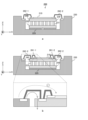
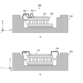
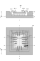
- 1A and 1B are an example of a cross-sectional view and a top view illustrating an example of a configuration of a semiconductor package according to a first embodiment of the present technology.
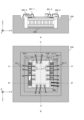
- 5A and 5B are an example of a cross-sectional view and a top view of another side of the semiconductor package according to the first embodiment of the present technology.
- 5A and 5B are an example of a cross-sectional view and a top view of another side of the semiconductor package according to the first embodiment of the present technology.
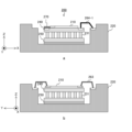
- 4A and 4B are an example of a cross-sectional view of a semiconductor package in a comparative example and an enlarged view of the semiconductor package in the first embodiment;
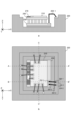
- 4A to 4C are diagrams for explaining a manufacturing method of a semiconductor package according to the first embodiment of the present technology.
- FIG. 4 is a flowchart showing an example of a method for manufacturing a semiconductor package according to the first embodiment of the present technology.
- 1 is a block diagram showing a configuration example of a semiconductor device according to a first embodiment of the present technology
- 13A and 13B are an example of a cross-sectional view and a top view illustrating an example of a configuration of a semiconductor package according to a second embodiment of the present technology.
- 13 is an example of a cross-sectional view of a semiconductor package according to a second embodiment of the present technology.
- 13A to 13C are diagrams for explaining a manufacturing method of a semiconductor package according to a second embodiment of the present technology.
- 13A and 13B are an example of a cross-sectional view and a top view illustrating an example of a configuration of a semiconductor package according to a third embodiment of the present technology.
- 13 is an example of a cross-sectional view of a semiconductor package according to a third embodiment of the present technology.
- 13A to 13C are diagrams for explaining a manufacturing method of a semiconductor package according to a third embodiment of the present technology.
- 13A and 13B are an example of a cross-sectional view and a top view illustrating an example of a configuration of a semiconductor package according to a fourth embodiment of the present technology.
- 13 is an example of a cross-sectional view of a semiconductor package according to a fourth embodiment of the present technology.
- 1 is a block diagram showing a schematic configuration example of a vehicle control system;
- FIG. 4 is an explanatory diagram showing an example of an installation position of an imaging unit.
- First embodiment (example of wiring via pads of a Peltier module) 2.
- Second embodiment (example of wiring via pads on a wiring board) 3.
- Third embodiment (example of wiring via pads on the heat dissipation side substrate of a Peltier module) 4.
- Fourth embodiment (an example in which the heat dissipation side substrate is eliminated and wiring is performed via the pads of the Peltier module) 5. Examples of applications to moving objects
- First embodiment [Example of semiconductor package configuration] 1A and 1B are an example of a cross-sectional view and a top view showing an example of a configuration of a semiconductor package 200 according to a first embodiment of the present technology.
- a is an example of a cross-sectional view of the semiconductor package 200
- b is an example of a top view of the semiconductor package 200.
- the semiconductor package 200 includes a semiconductor chip 210, a package substrate 220, and a Peltier module 230.
- X-axis a specific axis parallel to the chip plane of the semiconductor chip 210
- Z-axis a specific axis perpendicular to the chip plane
- Y-axis An axis perpendicular to the X-axis and Z-axis
- up the direction from the Peltier module 230 to the semiconductor chip 210.
- a is a cross-sectional view of the semiconductor package 200 taken along line A-A' in the figure, b, as viewed from the Y-axis direction.
- the package substrate 220 has a cavity.
- the depression in the region from coordinate X1 to coordinate X2 of a in the figure corresponds to the cavity.
- the underside of the Peltier module 230 is attached to the bottom surface of this cavity with adhesive 225.
- a ceramic substrate is used as the package substrate 220.
- a die bond material with relatively high thermal conductivity such as silver paste or conductive resin, is used as the adhesive 225.
- the Peltier module 230 comprises a heat absorption side substrate 240, a heat dissipation side substrate 250, and a predetermined number of Peltier elements 231.
- the heat dissipation side substrate 250 is adhered to the bottom surface of the cavity, and a predetermined number of Peltier elements 231 are arranged between the heat absorption side substrate 240 and the heat dissipation side substrate 250.
- a semiconductor chip 210 is mounted on the upper surface of the heat absorption side substrate 240.
- a CIS CMOS Image Sensor
- the Peltier element 231 transfers heat from the heat absorption side substrate 240 to the heat dissipation side substrate 250.
- multiple pads such as 211-1 and 211-2 are arranged on the top surface of the semiconductor chip 210.
- the area of the top surface of the Peltier module 230 (i.e., the top surface of the heat absorption side substrate 240) is larger than that of the semiconductor chip 210, and multiple pads such as 241-1 and 241-2 are arranged along the outer periphery of the semiconductor chip 210.
- multiple inner leads such as 221-1 and 221-2 are arranged on the top surface of the package substrate 220 along the outer periphery of the cavity.
- Pad 211-1 of semiconductor chip 210 is electrically connected to pad 241-1 of Peltier module 230 by wire 261-1, which is a power supply line.
- Pad 241-1 of Peltier module 230 is also electrically connected to inner lead 221-1 of package substrate 220 by wire 262-1, which is a power supply line.
- pad 211-2 of semiconductor chip 210 is electrically connected to pad 241-2 of Peltier module 230 by wire 261-2, which is a ground line.
- pad 241-2 of Peltier module 230 is electrically connected to inner lead 221-2 of package substrate 220 by wire 262-2, which is a ground line.
- wires 261-1 and 261-2 are an example of a first wire as described in the claims, and wires 262-1 and 262-2 are an example of a second wire as described in the claims.
- Pads 241-1 and 241-2 are an example of a relay pad as described in the claims.
- the power supply lines and ground lines for supplying power to the semiconductor chip 210 connect the semiconductor chip 210 to the package substrate 220 via the pads of the Peltier module 230. Power is supplied to the semiconductor chip 210 via these power supply lines and ground lines.
- wires for power supply can be commonly connected and bundled to one pad 241-1, and the pad 241-1 and the inner lead 221-1 can be connected by one wire. This makes it possible to reduce the number of wires between the Peltier module 230 and the package substrate 220. Also, since the wire connecting the package substrate 220 and the semiconductor chip 210 becomes a path for heat to move, this has the effect of making it thinner.
- the cavity is not sealed with glass or a frame, but it is possible to add glass or a frame to seal the cavity.
- the semiconductor package 200 with an unsealed structure is used, for example, in a vacuum.
- a is a cross-sectional view of the semiconductor package 200 taken along line B-B' in FIG. 2, b, as viewed from the Y-axis direction.
- the reference numerals in the vicinity of line A-A' in FIG. 1 have been omitted in FIG. 2, b.
- a number of pads such as 244-1 and 244-2 are arranged on the top surface of the Peltier module 230.
- a number of inner leads such as 224-1 and 224-2 are arranged on the top surface of the package substrate 220 along the outer periphery of the cavity.
- pad 244-1 of the Peltier module 230 is used as a positive terminal and is electrically connected to inner lead 224-1 of the package substrate 220 by wire 264-1.
- Pad 244-2 of the Peltier module 230 is used as a negative terminal and is electrically connected to inner lead 224-2 of the package substrate 220 by wire 264-2. Power is supplied to the Peltier module 230 via these wires. Note that wires 264-1 and 264-2 are an example of the fourth wire described in the claims.
- wires 264-1 and 264-2 for supplying power to the Peltier module 230 directly connect the Peltier module 230 to the package substrate 220.
- a in FIG. 3 is an example of a cross-sectional view of the semiconductor package 200 taken along line C-C' in b in the same figure, as viewed from the X-axis direction.
- the reference numerals in the vicinity of line A-A' in b in FIG. 1 have been omitted in b in FIG. 3.
- a plurality of pads such as 213 are arranged on the upper surface of the semiconductor chip 210.
- a plurality of inner leads such as 223 are arranged on the upper surface of the package substrate 220 along the outer periphery of the cavity.
- the pads 213 of the semiconductor chip 210 are electrically connected to the inner leads 223 of the package substrate 220 by wires 263, which are signal lines.
- Various electrical signals, such as clock signals, pixel signals, and control signals, are transmitted via the wires 263.
- the wires 263 are an example of the third wires described in the claims.
- the semiconductor chip 210 and the package substrate 220 are directly connected by a signal line.
- a comparative example is assumed in which the power supply line and ground line (262-1, 262-2) of the semiconductor chip 210 directly connect the semiconductor chip 210 and the package substrate 220 without passing through the pads of the Peltier module 230.
- the pads 244-1 and 244-2 for supplying power to the Peltier module 230 are not arranged on the heat absorption side substrate 240, and + and - power supply terminals (not shown) with the same function are arranged on the underside of the heat dissipation side substrate 250.
- the + and - power supply terminals are arranged on both sides of the white circle in FIG. 4a. An area where adhesive 225 is not applied is provided between these terminals to prevent short circuits.
- the Peltier module 230 transfers heat from the semiconductor chip 210 to the package substrate 220, cooling the semiconductor chip 210.
- a phenomenon called heat return may occur in which the heat transferred to the package substrate 220 returns to the semiconductor chip 210 via the signal lines, power lines, and ground lines.
- the semiconductor chip 210 has 40 signal lines and 200 power lines and ground lines, and a temperature rise of 4°C occurs due to heat return via these 240 total wires.
- the heat dissipation performance decreases by the amount of the temperature rise.
- the + and - power terminals are placed on the underside of the heat dissipation substrate 250, so the area of the adhesive 225 (silver paste, etc.) on the underside is reduced by the area between the terminals that is needed to prevent short circuits.
- the power supply line and ground line of the semiconductor chip 210 are connected to the package substrate 220 via the pads of the Peltier module 230.
- the heat can be transferred again to the heat dissipation substrate 250 before it returns to the semiconductor chip 210.
- the solid arrows in b in the figure indicate the heat transfer path, and the dotted arrows indicate the electron transfer path.
- the temperature rise due to the heat return can be calculated, for example, by the following formula. 4°C ⁇ 40/240 ⁇ 0.6°C
- the right side is a value obtained by rounding down the fraction after the first decimal place.
- the amount of temperature rise due to heat return can be suppressed compared to the comparative example. This improves heat dissipation performance.
- the signal lines are directly connected between the semiconductor chip 210 and the package substrate 220, the signal quality of the electrical signal transmitted by the signal lines does not deteriorate compared to the comparative example.
- pads 244-1 and 244-2 for power supply are arranged on the heat absorption side substrate 240, so there is no need to arrange power terminals on the underside of the heat dissipation side substrate 250.
- the area of adhesive 225 can be made larger than in the comparative example.
- FIG. 5A and 5B are diagrams for explaining a method for manufacturing a semiconductor package 200 according to the first embodiment of the present technology. First, as illustrated in FIG. 5A, a package substrate 220 having a cavity is manufactured.
- the Peltier module 230 is attached to the bottom surface of the cavity using adhesive 225 (such as silver paste).
- the semiconductor chip 210 is mounted on the upper surface of the Peltier module 230.
- wires 261 are wired to connect the semiconductor chip 210 and the Peltier module 230
- wires 262 are wired to connect the Peltier module 230 and the package substrate 220.
- the wires 261 in d of the same figure include wires 261-1 and 261-2.
- the wires 262 include wires 262-1 and 262-2.
- FIG. 6 is a flowchart showing an example of a method for manufacturing a semiconductor package in the first embodiment of the present technology.
- a package substrate 220 having a cavity is manufactured (step S901).
- a Peltier module 230 is attached to the bottom surface of the cavity (step S902), and a semiconductor chip 210 is mounted on the top surface of the Peltier module 230 (step S903).
- the semiconductor chip 210 is connected to the package substrate 220 by wire bonding (step S904).
- step S904 various subsequent steps are performed as necessary, and the manufacturing process for the semiconductor package 200 is completed.
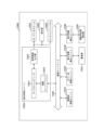
- FIG. 7 is a block diagram showing an example of the configuration of a semiconductor device 100 in the first embodiment of the present technology.
- This semiconductor device 100 includes the semiconductor package 200 described above and an external circuit 300.
- the external circuit 300 includes a power supply circuit 310, an image processing circuit 320, and a temperature control circuit 330.
- the semiconductor package 200 includes a semiconductor chip 210, a package substrate 220, and a Peltier module 230.
- Possible examples of the semiconductor device 100 include industrial equipment (such as inspection equipment), mirrorless cameras, smartphones, and notebook computers.
- the semiconductor chip 210 is provided with various circuits, such as a signal processing circuit 215.
- the signal processing circuit 215 performs various processes, such as CDS (Correlated Double Sampling) processing and AD (Analog to Digital) conversion, on the analog pixel signals to generate an image signal.
- CDS Correlated Double Sampling
- AD Analog to Digital
- Wire 261-1 which is a power supply line, connects the power supply terminal of the signal processing circuit 215 to pad 241-1 of the Peltier module 230, and wire 262-1 connects this pad 241-1 to an inner lead on the package substrate 220.
- Wire 261-2 which is a ground line, connects the ground terminal of the signal processing circuit 215 to pad 241-2 of the Peltier module 230, and wire 262-2 connects this pad 241-2 to an inner lead on the package substrate 220.
- the power supply circuit 310 supplies power to the circuits (such as the signal processing circuit 215) in the semiconductor chip 210 via these wires (power supply line and ground line).
- wires 263 connect the signal processing circuit 215 to the inner leads on the package substrate 220.
- the image processing circuit 320 exchanges electrical signals such as image signals and control signals with the signal processing circuit 215 via wires 263.
- This image processing circuit 320 performs various processes on the image signal, such as white balance processing and demosaic processing, and supplies the result to subsequent circuits.
- wires 264-1 and 264-2 connect the Peltier module 230 to the package substrate 220.
- the temperature control circuit 330 supplies power to the Peltier module 230 via these wires as necessary to drive it.
- the temperature control circuit 330 acquires the temperature of the semiconductor chip 210, and drives the Peltier module 230 when the temperature exceeds a predetermined upper limit.
- the power supply line and the ground line connect the semiconductor chip 210 and the package substrate 220 via the pads of the Peltier module 230, so that heat return can be suppressed. This can improve the heat dissipation performance of the semiconductor package 200.
- the power supply lines and ground lines are connected to the pads on the Peltier module 230, but a wiring board may be added to the Peltier module 230, and the power supply lines and ground lines may be connected to the pads on the wiring board.
- the semiconductor package 200 in this second embodiment differs from the first embodiment in that the power supply lines and ground lines are connected to pads on the wiring board.
- FIG. 8 shows an example of a cross-sectional view and a top view illustrating an example of a configuration of a semiconductor package in the second embodiment of the present technology.
- a is an example of a cross-sectional view of the semiconductor package 200
- b is an example of a top view of the semiconductor package 200.
- a in the figure is a cross-sectional view of the semiconductor package 200 cut along line segment A-A' in b in the figure, as viewed from the Y-axis direction.
- the semiconductor package 200 of the second embodiment differs from the first embodiment in that it further includes a predetermined number of wiring boards 270.
- the semiconductor chip 210 and wiring board 270 are attached to the top surface of the Peltier module 230.
- a number of pads such as 271-1 and 271-2 are arranged on the wiring board 270.
- the semiconductor chip 210 is connected to a pad 271-1 on the wiring board 270 by a wire 261-1 (power line).
- the pad 271-1 is connected to the package substrate 220 by a wire 262-1 (power line).
- the semiconductor chip 210 is also connected to a pad 271-2 on the wiring board 270 by a wire 261-2 (ground line).
- the pad 271-2 is also connected to the package substrate 220 by a wire 262-2 (ground line).
- a in FIG. 9 is an example of a cross-sectional view of the semiconductor package taken along line B-B' in FIG. 8 b, as viewed from the X-axis direction.
- the Peltier module 230 and the package substrate 220 are electrically connected by wires 264-1 and the like.
- FIG. 9 is an example of a cross-sectional view of the semiconductor package taken along line C-C' in b in FIG. 8, viewed from the X-axis direction.
- the semiconductor chip 210 and the package substrate 220 are directly connected by wire 263 (signal line).
- FIG. 10 is a diagram for explaining a method for manufacturing a semiconductor package in the second embodiment of the present technology. First, as shown in FIG. 10A, a package substrate 220 having a cavity is manufactured.
- the Peltier module 230 is attached to the bottom surface of the cavity using adhesive 225 (such as silver paste).
- the wiring board 270 and the semiconductor chip 210 are mounted on the upper surface of the Peltier module 230.
- wires 261 that connect the semiconductor chip 210 and the wiring board 270, and wires 262 that connect the wiring board 270 and the package substrate 220 are wired.
- the power supply lines and ground lines connect the semiconductor chip 210 and the package substrate 220 via the pads of the wiring board 270, so that heat return can be suppressed even when the wiring board 270 is used.
- the wires 264-1 and 264-2 for supplying power to the Peltier module 230 are connected to pads on the heat absorption side substrate 240, but heat return may occur via these wires.
- the semiconductor package 200 in this third embodiment differs from the second embodiment in that the wires 264-1 and 264-2 are connected to pads on the heat dissipation side substrate 250.
- FIG. 11 shows an example of a cross-sectional view and a top view illustrating an example of a configuration of a semiconductor package in the third embodiment of the present technology.
- a is an example of a cross-sectional view of the semiconductor package 200
- b is an example of a top view of the semiconductor package 200.
- a in the figure is a cross-sectional view of the semiconductor package 200 cut along line B-B' in b in the figure, as viewed from the Y-axis direction.
- the area of the heat dissipation side substrate 250 is larger than that of the heat absorption side substrate 240.
- pads 244-1 and 244-2 are not arranged on the upper surface of the heat absorption side substrate 240, and instead pads 254-1 and 254-2 are arranged on the upper surface of the heat dissipation side substrate 250.
- the pad 254-1 is used as a positive terminal and is electrically connected to the inner lead 224-1 of the package substrate 220 by a wire 264-1.
- the pad 254-2 is used as a negative terminal and is electrically connected to the inner lead 224-2 of the package substrate 220 by a wire 264-2. Power is supplied to the Peltier module 230 via these wires.
- wires 264-1 and 264-2 By connecting wires 264-1 and 264-2 to pads on the heat dissipation side substrate 250 that is farther from the semiconductor chip 210, it is possible to prevent the heat returning through these wires from being conducted to the semiconductor chip 210. In other words, it is possible to suppress the effects of heat return.
- a in FIG. 12 is an example of a cross-sectional view of the semiconductor package 200 taken along line A-A' in b in FIG. 11, as viewed from the Y-axis direction.
- wires 261-1, 262-1, etc. connect the semiconductor chip 210 and the package substrate 220 via pads on the wiring board 270.
- FIG. 12 is an example of a cross-sectional view of the semiconductor package 200 taken along line C-C' in b in FIG. 11 and viewed from the X-axis direction.
- the semiconductor chip 210 and the package substrate 220 are directly connected by wire 263 (signal line).
- FIG. 13 is a diagram for explaining a method for manufacturing a semiconductor package 200 in a third embodiment of the present technology. As shown in FIG. 13A, a package substrate 220 having a cavity is manufactured.
- the Peltier module 230 is attached to the bottom surface of the cavity using adhesive 225 (such as silver paste).
- the semiconductor chip 210 and the wiring board 270 are mounted on the upper surface of the Peltier module 230.
- wires 264-1 and the like are wired to connect the heat dissipation side substrate 250 and the package substrate 220.
- the wires 264-1 and 264-2 are connected to pads on the heat dissipation side substrate 250, so the effects of heat return via these wires can be suppressed.
- the heat absorption side substrate 240 and the heat dissipation side substrate 250 are disposed in the Peltier module 230, but the package substrate 220 can also be used as the substrate on the heat dissipation side instead of the heat dissipation side substrate 250.
- the semiconductor package 200 in this fourth embodiment differs from the first embodiment in that the heat dissipation side substrate 250 is omitted.
- FIG. 14 shows an example of a cross-sectional view and a top view illustrating an example of a configuration of a semiconductor package in the fourth embodiment of the present technology.
- a is an example of a cross-sectional view of the semiconductor package 200
- b is an example of a top view of the semiconductor package 200.
- a in the figure is a cross-sectional view of the semiconductor package 200 cut along line segment A-A' in b in the figure, as viewed from the Y-axis direction.
- the semiconductor package 200 in the fourth embodiment differs from the first embodiment in that the heat dissipation substrate 250 is not provided.
- the Peltier element 231 is disposed between the heat absorption side substrate 240 and the package substrate 220, and the Peltier element 231 transfers heat from the heat absorption side substrate 240 to the package substrate 220. In this way, the package substrate 220 is used as the substrate on the heat dissipation side.
- the heat dissipation substrate 250 can be eliminated. This allows the Peltier element to transfer heat directly to the package substrate 220, further improving heat dissipation performance. In addition, heat is dissipated from the underside of the package substrate 220, and it is preferable that the thickness dZ from the bottom of the cavity to the heat dissipation surface is small.
- a in FIG. 15 is an example of a cross-sectional view of the semiconductor package taken along line B-B' in FIG. 14 b, as viewed from the X-axis direction.
- the Peltier module 230 and the package substrate 220 are electrically connected by wires 264-1 and the like.
- FIG. 15 is an example of a cross-sectional view of the semiconductor package taken along line C-C' in b in FIG. 14, viewed from the X-axis direction.
- the semiconductor chip 210 and the package substrate 220 are directly connected by wire 263 (signal line).
- the second embodiment can be applied to the fourth embodiment.
- the package substrate 220 is used as the substrate on the heat dissipation side, so the heat dissipation substrate 250 can be reduced and the heat dissipation performance can be further improved.
- the technology according to the present disclosure can be applied to various products.
- the technology according to the present disclosure may be realized as a device mounted on any type of moving body such as an automobile, an electric vehicle, a hybrid electric vehicle, a motorcycle, a bicycle, a personal mobility device, an airplane, a drone, a ship, or a robot.
- FIG. 16 is a block diagram showing a schematic configuration example of a vehicle control system, which is an example of a mobile object control system to which the technology disclosed herein can be applied.
- the vehicle control system 12000 includes a plurality of electronic control units connected via a communication network 12001.
- the vehicle control system 12000 includes a drive system control unit 12010, a body system control unit 12020, an outside vehicle information detection unit 12030, an inside vehicle information detection unit 12040, and an integrated control unit 12050.
- Also shown as functional components of the integrated control unit 12050 are a microcomputer 12051, an audio/video output unit 12052, and an in-vehicle network I/F (interface) 12053.
- the drive system control unit 12010 controls the operation of devices related to the drive system of the vehicle according to various programs.
- the drive system control unit 12010 functions as a control device for a drive force generating device for generating the drive force of the vehicle, such as an internal combustion engine or a drive motor, a drive force transmission mechanism for transmitting the drive force to the wheels, a steering mechanism for adjusting the steering angle of the vehicle, and a braking device for generating a braking force for the vehicle.
- the body system control unit 12020 controls the operation of various devices installed in the vehicle body according to various programs.
- the body system control unit 12020 functions as a control device for a keyless entry system, a smart key system, a power window device, or various lamps such as headlamps, tail lamps, brake lamps, turn signals, and fog lamps.
- radio waves or signals from various switches transmitted from a portable device that replaces a key can be input to the body system control unit 12020.
- the body system control unit 12020 accepts the input of these radio waves or signals and controls the vehicle's door lock device, power window device, lamps, etc.
- the outside-vehicle information detection unit 12030 detects information outside the vehicle equipped with the vehicle control system 12000.
- the image capturing unit 12031 is connected to the outside-vehicle information detection unit 12030.
- the outside-vehicle information detection unit 12030 causes the image capturing unit 12031 to capture images outside the vehicle, and receives the captured images.
- the outside-vehicle information detection unit 12030 may perform object detection processing or distance detection processing for people, cars, obstacles, signs, or characters on the road surface, based on the received images.
- the imaging unit 12031 is an optical sensor that receives light and outputs an electrical signal according to the amount of light received.
- the imaging unit 12031 can output the electrical signal as an image, or as distance measurement information.
- the light received by the imaging unit 12031 may be visible light, or may be invisible light such as infrared light.
- the in-vehicle information detection unit 12040 detects information inside the vehicle.
- a driver state detection unit 12041 that detects the state of the driver is connected.
- the driver state detection unit 12041 includes, for example, a camera that captures an image of the driver, and the in-vehicle information detection unit 12040 may calculate the driver's degree of fatigue or concentration based on the detection information input from the driver state detection unit 12041, or may determine whether the driver is dozing off.
- the microcomputer 12051 can calculate control target values for the driving force generating device, steering mechanism, or braking device based on information inside and outside the vehicle acquired by the outside vehicle information detection unit 12030 or the inside vehicle information detection unit 12040, and output control commands to the drive system control unit 12010.
- the microcomputer 12051 can perform cooperative control aimed at realizing the functions of an Advanced Driver Assistance System (ADAS), including vehicle collision avoidance or impact mitigation, following driving based on the distance between vehicles, maintaining vehicle speed, vehicle collision warning, or vehicle lane departure warning.
- ADAS Advanced Driver Assistance System
- the microcomputer 12051 can also perform cooperative control for the purpose of autonomous driving, which allows the vehicle to travel autonomously without relying on the driver's operation, by controlling the driving force generating device, steering mechanism, braking device, etc. based on information about the surroundings of the vehicle acquired by the outside vehicle information detection unit 12030 or the inside vehicle information detection unit 12040.
- the microcomputer 12051 can also output control commands to the body system control unit 12020 based on information outside the vehicle acquired by the outside-vehicle information detection unit 12030. For example, the microcomputer 12051 can control the headlamps according to the position of a preceding vehicle or an oncoming vehicle detected by the outside-vehicle information detection unit 12030, and perform cooperative control aimed at preventing glare, such as switching high beams to low beams.
- the audio/image output unit 12052 transmits at least one output signal of audio and image to an output device capable of visually or audibly notifying the occupants of the vehicle or the outside of the vehicle of information.
- an audio speaker 12061, a display unit 12062, and an instrument panel 12063 are exemplified as output devices.
- the display unit 12062 may include, for example, at least one of an on-board display and a head-up display.
- FIG. 17 shows an example of the installation position of the imaging unit 12031.
- the imaging unit 12031 includes imaging units 12101, 12102, 12103, 12104, and 12105.
- the imaging units 12101, 12102, 12103, 12104, and 12105 are provided, for example, at the front nose, side mirrors, rear bumper, back door, and upper part of the windshield inside the vehicle cabin of the vehicle 12100.
- the imaging unit 12101 provided at the front nose and the imaging unit 12105 provided at the upper part of the windshield inside the vehicle cabin mainly acquire images of the front of the vehicle 12100.
- the imaging units 12102 and 12103 provided at the side mirrors mainly acquire images of the sides of the vehicle 12100.
- the imaging unit 12104 provided at the rear bumper or back door mainly acquires images of the rear of the vehicle 12100.
- the imaging unit 12105 provided at the upper part of the windshield inside the vehicle cabin is mainly used to detect leading vehicles, pedestrians, obstacles, traffic lights, traffic signs, lanes, etc.
- FIG. 17 shows an example of the imaging ranges of the imaging units 12101 to 12104.
- Imaging range 12111 indicates the imaging range of the imaging unit 12101 provided on the front nose
- imaging ranges 12112 and 12113 indicate the imaging ranges of the imaging units 12102 and 12103 provided on the side mirrors, respectively
- imaging range 12114 indicates the imaging range of the imaging unit 12104 provided on the rear bumper or back door.
- an overhead image of the vehicle 12100 viewed from above is obtained by superimposing the image data captured by the imaging units 12101 to 12104.
- At least one of the imaging units 12101 to 12104 may have a function of acquiring distance information.
- at least one of the imaging units 12101 to 12104 may be a stereo camera consisting of multiple imaging elements, or an imaging element having pixels for phase difference detection.
- the microcomputer 12051 can obtain the distance to each solid object within the imaging ranges 12111 to 12114 and the change in this distance over time (relative speed with respect to the vehicle 12100) based on the distance information obtained from the imaging units 12101 to 12104, and can extract as a preceding vehicle, in particular, the closest solid object on the path of the vehicle 12100 that is traveling in approximately the same direction as the vehicle 12100 at a predetermined speed (e.g., 0 km/h or faster). Furthermore, the microcomputer 12051 can set the inter-vehicle distance that should be maintained in advance in front of the preceding vehicle, and perform automatic braking control (including follow-up stop control) and automatic acceleration control (including follow-up start control). In this way, cooperative control can be performed for the purpose of automatic driving, which runs autonomously without relying on the driver's operation.
- automatic braking control including follow-up stop control
- automatic acceleration control including follow-up start control
- the microcomputer 12051 classifies and extracts three-dimensional object data on three-dimensional objects, such as two-wheeled vehicles, ordinary vehicles, large vehicles, pedestrians, utility poles, and other three-dimensional objects, based on the distance information obtained from the imaging units 12101 to 12104, and can use the data to automatically avoid obstacles.
- the microcomputer 12051 distinguishes obstacles around the vehicle 12100 into obstacles that are visible to the driver of the vehicle 12100 and obstacles that are difficult to see.
- the microcomputer 12051 determines the collision risk, which indicates the risk of collision with each obstacle, and when the collision risk is equal to or exceeds a set value and there is a possibility of a collision, it can provide driving assistance for collision avoidance by outputting an alarm to the driver via the audio speaker 12061 or the display unit 12062, or by forcibly decelerating or steering the vehicle to avoid a collision via the drive system control unit 12010.
- At least one of the imaging units 12101 to 12104 may be an infrared camera that detects infrared rays.
- the microcomputer 12051 can recognize a pedestrian by determining whether or not a pedestrian is present in the image captured by the imaging units 12101 to 12104. The recognition of such a pedestrian is performed, for example, by a procedure of extracting feature points in the image captured by the imaging units 12101 to 12104 as infrared cameras, and a procedure of performing pattern matching processing on a series of feature points that indicate the contour of an object to determine whether or not it is a pedestrian.
- the audio/image output unit 12052 controls the display unit 12062 to superimpose a rectangular contour line for emphasis on the recognized pedestrian.
- the audio/image output unit 12052 may also control the display unit 12062 to display an icon or the like indicating a pedestrian at a desired position.
- the technology disclosed herein can be applied to, for example, the imaging unit 12031.
- the semiconductor package 200 in FIG. 1 can be applied to the imaging unit 12031.
- image noise and the like can be reduced by improving heat dissipation performance, and a captured image that is easier to see can be obtained, thereby reducing driver fatigue.
- the present technology can also be configured as follows. (1) a semiconductor chip; A package substrate; a Peltier element for cooling a predetermined relay pad and the semiconductor chip; a first wire connecting the semiconductor chip and the relay pad; a semiconductor package including a second wire connecting the relay pad and the package substrate; (2) further comprising a third wire connecting the package substrate and the semiconductor chip to transmit an electrical signal; 2.
- the semiconductor device further includes a heat absorption side substrate on which the semiconductor chip is mounted, The semiconductor package according to (1), wherein the Peltier element is disposed between the heat absorption side substrate and the package substrate.
- a semiconductor chip A package substrate; a Peltier element for cooling a predetermined relay pad and the semiconductor chip; a first wire connecting the semiconductor chip and the relay pad; a second wire connecting the relay pad and the package substrate; a power supply circuit that supplies power to the semiconductor chip via the first wire and the second wire.
- (11) a step of disposing a Peltier module including a Peltier element for cooling a predetermined relay pad and a semiconductor chip on a package substrate; mounting the semiconductor chip on the Peltier module; a step of wiring a first wire that connects the semiconductor chip and the relay pad, and a second wire that connects the relay pad and the package substrate.
- Semiconductor device 100 Semiconductor device 200 Semiconductor package 210 Semiconductor chip 211-1, 211-2, 213, 241-1, 241-2, 244-1, 244-2, 254-1, 254-2, 271-1, 271-2 Pad 215 Signal processing circuit 220 Package substrate 221-1, 221-2, 223, 224-1, 224-2 Inner lead 225 Adhesive 230 Peltier module 231 Peltier element 240 Heat absorption side substrate 250 Heat dissipation side substrate 261, 261-1, 261-1a, 261-1b, 261-2, 262, 262-1, 262-2, 263, 264-1, 264-2 Wire 270 Wiring board 300 External circuit 310 Power supply circuit 320 Image processing circuit 330 Temperature control circuit 12031 Imaging unit
Landscapes
- Cooling Or The Like Of Semiconductors Or Solid State Devices (AREA)
Abstract
Description
1.第1の実施の形態(ペルチェモジュールのパッドを経由して配線する例)
2.第2の実施の形態(配線板のパッドを経由して配線する例)
3.第3の実施の形態(ペルチェモジュールの放熱側基板のパッドを経由して配線する例)
4.第4の実施の形態(放熱側基板を削減し、ペルチェモジュールのパッドを経由して配線する例)
5.移動体への応用例
[半導体パッケージの構成例]
図1は、本技術の第1の実施の形態における半導体パッケージ200の一構成例を示す断面図および上面図の一例である。同図におけるaは、半導体パッケージ200の断面図の一例であり、同図におけるbは、半導体パッケージ200の上面図の一例である。
4℃×40/240≒0.6℃
上式において、右辺は、小数点第2桁以降の端数を切り捨てた値である。
図5は、本技術の第1の実施の形態における半導体パッケージ200の製造方法を説明するための図である。まず、同図におけるaに例示するように、キャビティを有するパッケージ基板220が製造される。
上述の第1の実施の形態では、ペルチェモジュール230上のパッドに電源線やグランド線を接続していたが、ペルチェモジュール230に配線板が追加されることがあり、この配線板上のパッドに電源線やグランド線を接続することもできる。この第2の実施の形態における半導体パッケージ200は、電源線やグランド線が配線板上のパッドに接続される点において第1の実施の形態と異なる。
上述の第2の実施の形態では、ペルチェモジュール230への電源供給のためのワイヤ264-1および264-2を吸熱側基板240のパッドに接続していたが、これらのワイヤを介して熱戻りが生じることがある。この第3の実施の形態における半導体パッケージ200は、ワイヤ264-1および264-2を放熱側基板250のパッドに接続する点において第2の実施の形態と異なる。
上述の第1の実施の形態では、ペルチェモジュール230内に、吸熱側基板240および放熱側基板250を配置していたが、放熱側基板250の代わりにパッケージ基板220を放熱側の基板として用いることもできる。この第4の実施の形態における半導体パッケージ200は、放熱側基板250を削減した点において第1の実施の形態と異なる。
本開示に係る技術(本技術)は、様々な製品へ応用することができる。例えば、本開示に係る技術は、自動車、電気自動車、ハイブリッド電気自動車、自動二輪車、自転車、パーソナルモビリティ、飛行機、ドローン、船舶、ロボット等のいずれかの種類の移動体に搭載される装置として実現されてもよい。
(1)半導体チップと、
パッケージ基板と、
所定の中継パッドと前記半導体チップとを冷却するペルチェ素子と、
前記半導体チップと前記中継パッドとを接続する第1ワイヤと、
前記中継パッドと前記パッケージ基板とを接続する第2ワイヤと
を具備する半導体パッケージ。
(2)前記パッケージ基板と前記半導体チップとを接続して電気信号を伝送する第3ワイヤをさらに具備し、
前記第1ワイヤおよび前記第2ワイヤを介して前記半導体チップに電源が供給される
前記(1)記載の半導体パッケージ。
(3)1つの前記中継パッドに複数本の前記第1ワイヤと1本の前記第2ワイヤとが接続される前記(1)または(2)に記載の半導体パッケージ。
(4)前記半導体チップがマウントされた吸熱側基板と、
前記パッケージ基板に接着剤により接着された放熱側基板と
をさらに具備し、
前記ペルチェ素子は、前記吸熱側基板と前記放熱側基板との間に配置される
前記(1)から(3)のいずれかに記載の半導体パッケージ。
(5)前記中継パッドは、前記吸熱側基板に配置される
前記(4)記載の半導体パッケージ。
(6)前記吸熱側基板に接着された配線板をさらに具備し、
前記中継パッドは、前記配線板に配置される
前記(4)記載の半導体パッケージ。
(7)前記吸熱側基板と前記パッケージ基板とを接続する第4ワイヤをさらに具備し、
前記第4ワイヤを介して前記ペルチェ素子に電源が供給される
前記(4)から(6)のいずれかに記載の半導体パッケージ。
(8)前記放熱側基板と前記パッケージ基板とを接続する第4ワイヤをさらに具備し、
前記第4ワイヤを介して前記ペルチェ素子に電源が供給される
前記(4)から(6)のいずれかに記載の半導体パッケージ。
(9)前記半導体チップがマウントされた吸熱側基板をさらに具備し、
前記ペルチェ素子は、前記吸熱側基板と前記パッケージ基板との間に配置される
前記(1)記載の半導体パッケージ。
(10)半導体チップと、
パッケージ基板と、
所定の中継パッドと前記半導体チップとを冷却するペルチェ素子と、
前記半導体チップと前記中継パッドとを接続する第1ワイヤと、
前記中継パッドと前記パッケージ基板とを接続する第2ワイヤと、
前記第1ワイヤおよび前記第2ワイヤを介して前記半導体チップに電源を供給する電源回路と
を具備する半導体装置。
(11)所定の中継パッドと半導体チップとを冷却するペルチェ素子を含むペルチェモジュールをパッケージ基板に配置する手順と、
前記ペルチェモジュールに前記半導体チップをマウントする手順と、
前記半導体チップと前記中継パッドとを接続する第1ワイヤと前記中継パッドと前記パッケージ基板とを接続する第2ワイヤとを配線する手順と
を具備する半導体パッケージの製造方法。
200 半導体パッケージ
210 半導体チップ
211-1、211-2、213、241-1、241-2、244-1、244-2、254-1、254-2、271-1、271-2 パッド
215 信号処理回路
220 パッケージ基板
221-1、221-2、223、224-1、224-2 インナーリード
225 接着剤
230 ペルチェモジュール
231 ペルチェ素子
240 吸熱側基板
250 放熱側基板
261、261-1、261-1a、261-1b、261-2、262、262-1、262-2、263、264-1、264-2 ワイヤ
270 配線板
300 外部回路
310 電源回路
320 画像処理回路
330 温度制御回路
12031 撮像部
Claims (11)
- 半導体チップと、
パッケージ基板と、
所定の中継パッドと前記半導体チップとを冷却するペルチェ素子と、
前記半導体チップと前記中継パッドとを接続する第1ワイヤと、
前記中継パッドと前記パッケージ基板とを接続する第2ワイヤと
を具備する半導体パッケージ。 - 前記パッケージ基板と前記半導体チップとを接続して電気信号を伝送する第3ワイヤをさらに具備し、
前記第1ワイヤおよび前記第2ワイヤを介して前記半導体チップに電源が供給される
請求項1記載の半導体パッケージ。 - 1つの前記中継パッドに複数本の前記第1ワイヤと1本の前記第2ワイヤとが接続される請求項1記載の半導体パッケージ。
- 前記半導体チップがマウントされた吸熱側基板と、
前記パッケージ基板に接着剤により接着された放熱側基板と
をさらに具備し、
前記ペルチェ素子は、前記吸熱側基板と前記放熱側基板との間に配置される
請求項1記載の半導体パッケージ。 - 前記中継パッドは、前記吸熱側基板に配置される
請求項4記載の半導体パッケージ。 - 前記吸熱側基板に接着された配線板をさらに具備し、
前記中継パッドは、前記配線板に配置される
請求項4記載の半導体パッケージ。 - 前記吸熱側基板と前記パッケージ基板とを接続する第4ワイヤをさらに具備し、
前記第4ワイヤを介して前記ペルチェ素子に電源が供給される
請求項4記載の半導体パッケージ。 - 前記放熱側基板と前記パッケージ基板とを接続する第4ワイヤをさらに具備し、
前記第4ワイヤを介して前記ペルチェ素子に電源が供給される
請求項4記載の半導体パッケージ。 - 前記半導体チップがマウントされた吸熱側基板をさらに具備し、
前記ペルチェ素子は、前記吸熱側基板と前記パッケージ基板との間に配置される
請求項1記載の半導体パッケージ。 - 半導体チップと、
パッケージ基板と、
所定の中継パッドと前記半導体チップとを冷却するペルチェ素子と、
前記半導体チップと前記中継パッドとを接続する第1ワイヤと、
前記中継パッドと前記パッケージ基板とを接続する第2ワイヤと、
前記第1ワイヤおよび前記第2ワイヤを介して前記半導体チップに電源を供給する電源回路と
を具備する半導体装置。 - 所定の中継パッドと半導体チップとを冷却するペルチェ素子を含むペルチェモジュールをパッケージ基板に配置する手順と、
前記ペルチェモジュールに前記半導体チップをマウントする手順と、
前記半導体チップと前記中継パッドとを接続する第1ワイヤと前記中継パッドと前記パッケージ基板とを接続する第2ワイヤとを配線する手順と
を具備する半導体パッケージの製造方法。
Priority Applications (1)
| Application Number | Priority Date | Filing Date | Title |
|---|---|---|---|
| CN202480015913.2A CN120814050A (zh) | 2023-03-06 | 2024-01-10 | 半导体封装、半导体器件及半导体封装的制造方法 |
Applications Claiming Priority (2)
| Application Number | Priority Date | Filing Date | Title |
|---|---|---|---|
| JP2023033324 | 2023-03-06 | ||
| JP2023-033324 | 2023-03-06 |
Publications (1)
| Publication Number | Publication Date |
|---|---|
| WO2024185282A1 true WO2024185282A1 (ja) | 2024-09-12 |
Family
ID=92674777
Family Applications (1)
| Application Number | Title | Priority Date | Filing Date |
|---|---|---|---|
| PCT/JP2024/000246 Ceased WO2024185282A1 (ja) | 2023-03-06 | 2024-01-10 | 半導体パッケージ、半導体装置、および、半導体パッケージの製造方法 |
Country Status (2)
| Country | Link |
|---|---|
| CN (1) | CN120814050A (ja) |
| WO (1) | WO2024185282A1 (ja) |
Citations (5)
| Publication number | Priority date | Publication date | Assignee | Title |
|---|---|---|---|---|
| JPH0738019A (ja) * | 1993-07-23 | 1995-02-07 | Hamamatsu Photonics Kk | 冷却型固体撮像装置 |
| JP2000340723A (ja) * | 1999-05-31 | 2000-12-08 | Toshiba Corp | 半導体スイッチ装置およびこの半導体スイッチ装置を用いた電力変換装置 |
| JP2001249166A (ja) * | 2000-03-03 | 2001-09-14 | Nec Corp | 回路装置、パッケージ部材、回路製造方法、回路試験方法および装置 |
| JP2003258325A (ja) * | 2002-03-05 | 2003-09-12 | Aisin Seiki Co Ltd | 熱電モジュールの製造方法および熱電モジュール |
| WO2021140920A1 (ja) * | 2020-01-08 | 2021-07-15 | ソニーセミコンダクタソリューションズ株式会社 | 固体撮像装置、撮像装置及び撮像システム |
-
2024
- 2024-01-10 CN CN202480015913.2A patent/CN120814050A/zh active Pending
- 2024-01-10 WO PCT/JP2024/000246 patent/WO2024185282A1/ja not_active Ceased
Patent Citations (5)
| Publication number | Priority date | Publication date | Assignee | Title |
|---|---|---|---|---|
| JPH0738019A (ja) * | 1993-07-23 | 1995-02-07 | Hamamatsu Photonics Kk | 冷却型固体撮像装置 |
| JP2000340723A (ja) * | 1999-05-31 | 2000-12-08 | Toshiba Corp | 半導体スイッチ装置およびこの半導体スイッチ装置を用いた電力変換装置 |
| JP2001249166A (ja) * | 2000-03-03 | 2001-09-14 | Nec Corp | 回路装置、パッケージ部材、回路製造方法、回路試験方法および装置 |
| JP2003258325A (ja) * | 2002-03-05 | 2003-09-12 | Aisin Seiki Co Ltd | 熱電モジュールの製造方法および熱電モジュール |
| WO2021140920A1 (ja) * | 2020-01-08 | 2021-07-15 | ソニーセミコンダクタソリューションズ株式会社 | 固体撮像装置、撮像装置及び撮像システム |
Also Published As
| Publication number | Publication date |
|---|---|
| CN120814050A (zh) | 2025-10-17 |
Similar Documents
| Publication | Publication Date | Title |
|---|---|---|
| JP7499242B2 (ja) | 半導体パッケージ、および、電子装置 | |
| US12563317B2 (en) | Imaging element and imaging device | |
| US20240063244A1 (en) | Semiconductor package, electronic device, and method of manufacturing semiconductor package | |
| US11670625B2 (en) | Imaging unit having a stacked structure and electronic apparatus including the imaging unit | |
| US12310132B2 (en) | Semiconductor package, semiconductor package manufacturing method, and electronic device | |
| WO2024185282A1 (ja) | 半導体パッケージ、半導体装置、および、半導体パッケージの製造方法 | |
| JP7630428B2 (ja) | 半導体パッケージ | |
| WO2019198385A1 (ja) | 撮像装置およびその製造方法、電子機器 | |
| JP7624393B2 (ja) | 半導体パッケージ、電子装置、および、半導体パッケージの製造方法 | |
| US20250251238A1 (en) | Semiconductor package and module | |
| WO2026018560A1 (ja) | 半導体パッケージ、半導体装置、および、半導体パッケージの製造方法 | |
| WO2024224806A1 (ja) | 半導体パッケージ、半導体装置、および、半導体パッケージの製造方法 | |
| WO2024257483A1 (ja) | 半導体パッケージ、および、半導体パッケージの製造方法 | |
| WO2024224807A1 (ja) | 半導体パッケージ、および、半導体パッケージの製造方法 | |
| WO2024106011A1 (ja) | 半導体パッケージ、電子装置、および、半導体パッケージの制御方法 | |
| WO2025158775A1 (ja) | 半導体パッケージ、半導体装置、および、半導体パッケージの製造方法 | |
| WO2024122177A1 (ja) | 半導体パッケージ、および、半導体パッケージの製造方法 | |
| WO2024075398A1 (ja) | カメラモジュール、および、撮像装置 | |
| WO2025115400A1 (ja) | 半導体パッケージ、半導体装置、および、半導体パッケージの製造方法 | |
| WO2024057709A1 (ja) | 半導体パッケージ、および、電子装置 | |
| WO2026004347A1 (ja) | 光学パッケージ、モジュール、および、光学パッケージの製造方法 | |
| WO2024111248A1 (ja) | 半導体パッケージ、光学装置、および、半導体パッケージの製造方法 | |
| CN115250338A (zh) | 光检测设备 | |
| WO2025234202A1 (ja) | 半導体パッケージ、半導体装置、および、半導体パッケージの製造方法 | |
| TW202610497A (zh) | 半導體封裝、半導體裝置、及半導體封裝之製造方法 |
Legal Events
| Date | Code | Title | Description |
|---|---|---|---|
| 121 | Ep: the epo has been informed by wipo that ep was designated in this application |
Ref document number: 24766657 Country of ref document: EP Kind code of ref document: A1 |
|
| WWE | Wipo information: entry into national phase |
Ref document number: 202480015913.2 Country of ref document: CN |
|
| NENP | Non-entry into the national phase |
Ref country code: DE |
|
| WWP | Wipo information: published in national office |
Ref document number: 202480015913.2 Country of ref document: CN |
|
| 122 | Ep: pct application non-entry in european phase |
Ref document number: 24766657 Country of ref document: EP Kind code of ref document: A1 |