WO2024176950A1 - 半導体レーザ装置、光源モジュール及び光源モジュールの製造方法 - Google Patents
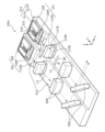
半導体レーザ装置、光源モジュール及び光源モジュールの製造方法 Download PDFInfo
- Publication number
- WO2024176950A1 WO2024176950A1 PCT/JP2024/005360 JP2024005360W WO2024176950A1 WO 2024176950 A1 WO2024176950 A1 WO 2024176950A1 JP 2024005360 W JP2024005360 W JP 2024005360W WO 2024176950 A1 WO2024176950 A1 WO 2024176950A1
- Authority
- WO
- WIPO (PCT)
- Prior art keywords
- semiconductor laser
- cylindrical lens
- lens
- plane
- installation plane
- Prior art date
- Legal status (The legal status is an assumption and is not a legal conclusion. Google has not performed a legal analysis and makes no representation as to the accuracy of the status listed.)
- Ceased
Links
Images
























Classifications
-
- H—ELECTRICITY
- H01—ELECTRIC ELEMENTS
- H01S—DEVICES USING THE PROCESS OF LIGHT AMPLIFICATION BY STIMULATED EMISSION OF RADIATION [LASER] TO AMPLIFY OR GENERATE LIGHT; DEVICES USING STIMULATED EMISSION OF ELECTROMAGNETIC RADIATION IN WAVE RANGES OTHER THAN OPTICAL
- H01S5/00—Semiconductor lasers
- H01S5/02—Structural details or components not essential to laser action
- H01S5/022—Mountings; Housings
- H01S5/0225—Out-coupling of light
- H01S5/02253—Out-coupling of light using lenses
-
- H—ELECTRICITY
- H01—ELECTRIC ELEMENTS
- H01S—DEVICES USING THE PROCESS OF LIGHT AMPLIFICATION BY STIMULATED EMISSION OF RADIATION [LASER] TO AMPLIFY OR GENERATE LIGHT; DEVICES USING STIMULATED EMISSION OF ELECTROMAGNETIC RADIATION IN WAVE RANGES OTHER THAN OPTICAL
- H01S5/00—Semiconductor lasers
- H01S5/02—Structural details or components not essential to laser action
- H01S5/022—Mountings; Housings
- H01S5/0235—Method for mounting laser chips
- H01S5/02355—Fixing laser chips on mounts
-
- H—ELECTRICITY
- H01—ELECTRIC ELEMENTS
- H01S—DEVICES USING THE PROCESS OF LIGHT AMPLIFICATION BY STIMULATED EMISSION OF RADIATION [LASER] TO AMPLIFY OR GENERATE LIGHT; DEVICES USING STIMULATED EMISSION OF ELECTROMAGNETIC RADIATION IN WAVE RANGES OTHER THAN OPTICAL
- H01S5/00—Semiconductor lasers
- H01S5/40—Arrangement of two or more semiconductor lasers, not provided for in groups H01S5/02 - H01S5/30
Definitions
- This disclosure relates to a semiconductor laser device, a light source module, and a method for manufacturing a light source module.
- Patent document 1 discloses a semiconductor laser device that includes a semiconductor laser element and a collimator lens that collimates the laser light emitted from the semiconductor laser element in the fast axis direction.
- the position adjustment precision of the collimator lens in the fast axis direction of the semiconductor laser device is low, so when a light source module includes multiple semiconductor laser devices, the positional misalignment between the target, such as an optical fiber, and the laser light becomes large, resulting in many semiconductor laser devices with low coupling efficiency between the laser light and the target. If many semiconductor laser devices with low coupling efficiency between the laser light and the target occur, the coupling efficiency of the light source module will decrease.
- the present disclosure therefore aims to easily increase the coupling efficiency of light source modules.
- a semiconductor laser device includes a semiconductor laser element that emits laser light, and a lens unit having a first cylindrical lens and an installation plane, the semiconductor laser element has an active layer, the first cylindrical lens receives the laser light and reduces the spread angle of the laser light in the fast axis direction, the installation plane is fixed to a first installation plane, the generatrix of the first cylindrical lens is inclined with respect to the first installation plane, and the angle ⁇ between the generatrix and the active layer is
- a semiconductor laser device includes a semiconductor laser element that emits laser light, and a lens unit having a first cylindrical lens and an installation plane, the semiconductor laser element has an active layer, the first cylindrical lens receives the laser light and reduces the spread angle of the laser light in the fast axis direction, the installation plane is fixed to a first installation plane, the generatrix of the first cylindrical lens is inclined with respect to the installation plane, and the angle ⁇ between the generatrix and the active layer is
- a light source module includes a plurality of the semiconductor laser devices described above, and the laser light emitted from the semiconductor laser elements included in each of the plurality of semiconductor laser devices is combined.
- a manufacturing method of a light source module is a manufacturing method of a light source module, the light source module comprising a semiconductor laser element that emits laser light, a first mounting plane, and a lens portion having a first cylindrical lens and a mounting plane, the semiconductor laser element having an active layer, the first cylindrical lens reducing the spread angle of the laser light in the fast axis direction, the mounting plane being fixed to the first mounting plane, and the manufacturing method further comprising the steps of:
- the method includes a placement step of placing the lens unit on the first installation plane so as to be inclined with respect to the installation plane, an alignment step of making the laser light emitted from the semiconductor laser element enter the first cylindrical lens and moving the placed lens unit in two mutually orthogonal directions parallel to the first installation plane, and a fixing step of fixing the moved lens unit to the first installation plane, and in the placement step, the angle ⁇ between the generatrix and the active layer is
- a method for manufacturing a light source module is a method for manufacturing a light source module, the light source module comprising a semiconductor laser element that emits laser light, a first mounting plane, and a lens unit having a first cylindrical lens and a mounting plane, the semiconductor laser element having an active layer, the first cylindrical lens reducing the spread angle of the laser light in the fast axis direction, and the mounting plane being fixed to the first mounting plane, the manufacturing method including an arrangement step of arranging the lens unit on the first mounting plane so that the generatrix of the first cylindrical lens is inclined with respect to the mounting plane, an alignment step of causing the laser light emitted from the semiconductor laser element to be incident on the first cylindrical lens and moving the arranged lens unit in two mutually orthogonal directions parallel to the first mounting plane, and a fixing step of fixing the moved lens unit to the first mounting plane, and in the arrangement step, the angle ⁇ between the generatrix and the active layer is
- the coupling efficiency of the light source module can be easily increased.
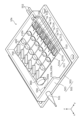
- FIG. 1 is a perspective view showing an overall configuration of a light source module according to a first embodiment.
- FIG. 2 is a perspective view showing a configuration of the semiconductor laser device according to the first embodiment.
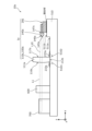
- FIG. 3 is a front view showing the configuration of the semiconductor laser device according to the first embodiment.
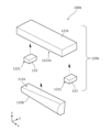
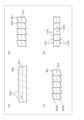
- FIG. 4 is an exploded perspective view of a lens unit according to the first embodiment.
- FIG. 5 is a cross-sectional view showing a cut surface of the semiconductor laser device taken along line VV in FIG.
- FIG. 6 is an enlarged cross-sectional view showing the light emitting region and the first cylindrical lens in FIG.
- FIG. 7 is a schematic diagram showing steps of a manufacturing method near the semiconductor laser device of the light source module according to the first embodiment.
- FIG. 1 is a perspective view showing an overall configuration of a light source module according to a first embodiment.
- FIG. 2 is a perspective view showing a configuration of the semiconductor laser device according to the first embodiment.
- FIG. 3 is a front view showing the configuration of
- FIG. 8 is a schematic diagram showing steps of a manufacturing method for the vicinity of the semiconductor laser device of the light source module according to the first embodiment.
- FIG. 9 is a schematic diagram showing steps of a manufacturing method near the semiconductor laser device of the light source module according to the first embodiment.
- FIG. 10 is a schematic diagram showing steps of a manufacturing method near the semiconductor laser device of the light source module according to the first embodiment.
- FIG. 11 is a schematic diagram showing steps of a manufacturing method near the semiconductor laser device of the light source module according to the first embodiment.
- FIG. 12 is a diagram showing the relationship between the angle ⁇ and the amount of movement ⁇ z in the z-axis direction and the amount of movement ⁇ x in the x-axis direction of the first cylindrical lens according to the first embodiment.
- FIG. 13 is a front view showing an example in which the lens portion moves in the x-axis direction in the alignment step according to the first embodiment.
- FIG. 14 is a diagram showing the relationship between the angle ⁇ , the amount of movement ⁇ z in the z-axis direction, and the amount of movement ⁇ x in the x-axis direction according to the first embodiment.
- FIG. 15 is a cross-sectional view showing a semiconductor laser device according to a comparative example.
- FIG. 16 is a diagram showing the relationship between the change in position of the FAC lens in the z-axis direction and the coupling efficiency in a light source module including a semiconductor laser device according to a comparative example.
- FIG. 17 is a diagram showing a table for explaining the simulation conditions of FIG. FIG.
- FIG. 18 is a diagram showing the results of a simulation of the light intensity distribution when the angle ⁇ is 0° and the angle ⁇ is 2° according to the first embodiment.
- Figure 19A is a diagram showing the results of a simulation calculation of the change in coupling efficiency when the first cylindrical lens of a semiconductor laser device of embodiment 1 is inclined with respect to the installation plane and the first cylindrical lens is moved along the installation plane.
- FIG. 19B is a diagram showing the results of calculations, by simulation, of the maximum value of the coupling efficiency when the angle ⁇ according to the first embodiment is changed.
- FIG. 20 is a front view showing a configuration of a semiconductor laser device according to a first modification of the first embodiment.
- FIG. 21 is a front view showing a configuration of a semiconductor laser device according to the second modification of the first embodiment.
- FIG. 22 is a diagram showing the shape of a first cylindrical lens according to the second modification of the first embodiment.
- FIG. 23 is an exploded perspective view of a lens portion according to the second modification of the first embodiment.
- FIG. 24 is a front view showing a configuration of a semiconductor laser device according to a third modification of the first embodiment.
- FIG. 25 is a front view showing a configuration of a semiconductor laser device according to the fourth modification of the first embodiment.
- FIG. 26 is an enlarged front view of the periphery of the second support member in region XXVI of FIG. 25.
- FIG. FIG. 27 is a front view of a semiconductor laser device according to the study example.
- FIG. 28 is a perspective view showing an overall configuration of a light source module according to the second embodiment.
- FIG. 29 is a perspective view showing a configuration of a semiconductor laser device according to the second embodiment.
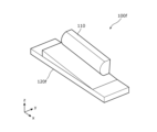
- FIG. 30 is a perspective view of a lens unit according to the second embodiment.
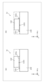
- FIG. 31 is a schematic diagram showing steps of a manufacturing method for the vicinity of the semiconductor laser device of the light source module according to the second embodiment.
- FIG. 32 is a schematic diagram showing steps of a manufacturing method near the semiconductor laser device of the light source module according to the second embodiment.
- FIG. 33 is a schematic diagram showing steps of a manufacturing method for the vicinity of the semiconductor laser device of the light source module according to the second embodiment.
- FIG. 34 is a schematic diagram showing steps of a manufacturing method near the semiconductor laser device of the light source module according to the second embodiment.
- FIG. 35 is a front view showing a configuration of a semiconductor laser device according to a first modification of the second embodiment.
- FIG. 36 is a front view showing a configuration of a semiconductor laser device according to a second modification of the second embodiment.
- FIG. 37 is a front view showing a configuration of a semiconductor laser device according to a third modification of the second embodiment.
- FIG. 38 is a perspective view showing a part of a light source module according to embodiment 3.
- FIG. 39 is a front view of a first cylindrical lens and a second cylindrical lens according to the third embodiment.
- FIG. 40 is a diagram showing the relationship between the angle ⁇ and the angle ⁇ and the coupling efficiency according to the third embodiment.
- FIG. 41A is a diagram showing a table explaining the simulation conditions of FIG. FIG.
- FIG. 41B is a diagram showing a change in coupling efficiency when the lens portion is moved in the x-axis direction in the light source module according to embodiment 3.
- FIG. 42 is a perspective view showing a part of a light source module according to a modification of the third embodiment.
- FIG. 43 is a perspective view showing a semiconductor laser device according to the fourth embodiment.
- FIG. 44 is an exploded front view of a lens unit and a fixing member according to the fourth embodiment.
- FIG. 45 is a schematic diagram showing steps of a manufacturing method for the vicinity of the semiconductor laser device of the light source module according to the fourth embodiment.
- FIG. 46 is a schematic diagram showing steps of a manufacturing method for the vicinity of the semiconductor laser device of the light source module according to the fourth embodiment.
- FIG. 47 is a schematic diagram showing steps of a manufacturing method for the vicinity of the semiconductor laser device of the light source module according to the fourth embodiment.
- FIG. 48A is a schematic diagram showing a process of a manufacturing method near the semiconductor laser device of the light source module according to embodiment 4.
- 48B is a diagram showing a change in coupling efficiency when the lens unit moves in the x-axis direction along the installation plane when the angle ⁇ is 0°, 0.5°, 2°, and 5° under the condition of No. 1 in FIG. 17 for a light source module according to embodiment 4.
- FIG. 49 is a front view showing a configuration of a semiconductor laser device according to a first modification of the fourth embodiment.
- FIG. 48A is a schematic diagram showing a process of a manufacturing method near the semiconductor laser device of the light source module according to embodiment 4.
- 48B is a diagram showing a change in coupling efficiency when the lens unit moves in the x-axis direction along the installation plane when the angle ⁇ is 0°, 0.5°,
- FIG. 50 is a schematic diagram showing steps of a manufacturing method for the vicinity of the semiconductor laser device of the light source module according to the first modification of the fourth embodiment.
- FIG. 51 is a schematic diagram showing steps of a manufacturing method for the vicinity of the semiconductor laser device of the light source module according to the first modification of the fourth embodiment.
- FIG. 52 is a schematic diagram showing steps of a manufacturing method for the vicinity of the semiconductor laser device of the light source module according to the first modification of the fourth embodiment.
- FIG. 53 is a schematic diagram showing steps of a manufacturing method for the vicinity of the semiconductor laser device of the light source module according to the first modification of the fourth embodiment.
- FIG. 54 is a top view showing a configuration of a semiconductor laser device according to the second modification of the fourth embodiment.
- FIG. 55 is a front view showing a configuration of a semiconductor laser device according to the second modification of the fourth embodiment.
- FIG. 56 is a front view showing the configuration of a semiconductor laser device according to the fifth embodiment.
- FIG. 57 is a side view showing the configuration of a semiconductor laser device according to the fifth embodiment.
- FIG. 58 is a top view showing a configuration of a semiconductor laser device according to the fifth embodiment.
- FIG. 59 is a perspective view showing the overall configuration of a light source module according to embodiment 6.
- FIG. 60 is a perspective view of a semiconductor laser device provided in a light source module according to the sixth embodiment.
- FIG. 61 is a side view of a semiconductor laser device according to the sixth embodiment.
- FIG. 62 is a front view showing a manufacturing method of the first cylindrical lens according to the sixth embodiment.
- each figure is a schematic diagram and is not necessarily an exact illustration. Therefore, for example, the scales of each figure do not necessarily match.
- the same reference numerals are used for substantially the same configuration, and duplicate explanations are omitted or simplified.
- the terms “above” and “below” do not refer to the upward direction (vertically upward) and downward direction (vertically downward) in an absolute spatial sense, but are used as terms defined by a relative positional relationship based on the stacking order in a stacked configuration. Furthermore, the terms “above” and “below” are applied not only to cases where two components are arranged with a gap between them and another component exists between the two components, but also to cases where two components are arranged closely together and are in contact with each other.
- the x-axis, y-axis, and z-axis represent the three axes of a three-dimensional Cartesian coordinate system relating to the semiconductor laser element.
- the positive direction of the z-axis may be referred to as the upper direction, and the negative direction of the z-axis may be referred to as the lower direction.
- the upper surface may be referred to as the upper surface, and the lower surface may be referred to as the lower surface.
- the direction of travel along the optical axis of the laser light immediately after being emitted from the semiconductor laser element is the negative y-axis direction
- the direction parallel to the fast axis of the laser light immediately after being emitted from the semiconductor laser element is the z-axis direction
- the direction parallel to the slow axis of the laser light immediately after being emitted from the semiconductor laser element is the x-axis direction.
- top view means that the semiconductor laser device is viewed from the positive side of the z-axis, and the view in this state is called a top view.
- Front view means that the semiconductor laser device is viewed from the negative side of the y-axis, and the view in this state is called a front view.
- Side view means that the semiconductor laser device is viewed from the positive or negative side of the x-axis, and the view in this state is called a side view.
- FIG. 1 is a perspective view showing the overall configuration of a light source module 10 according to this embodiment.
- the light source module 10 includes a case 501, a plurality of semiconductor laser devices (here, semiconductor laser devices 1, 2, 3, 4, 5, and 6), a plurality of slow axis collimator lenses 600 (SAC lenses 600), a plurality of reflecting mirrors 700, a focusing lens 800, an optical fiber 550, and a pair of lead pins 552.
- the optical fiber 550 has a core 550a that guides the laser light.
- the light source module 10 also includes a boot 551.
- the light source module 10 also includes a staircase base 510.
- the light source module 10 is a module that can spatially combine and emit laser light emitted from each of a plurality of semiconductor laser devices by an optical system.
- the combined laser light is incident on the core 550a, which is the object, in the light source module 10, and the laser light propagates through the optical fiber 550 and is emitted from the light source module 10 to the outside. In other words, the laser light is incident on the core 550a at this time as being combined.
- the light source module 10 may also be a module that can combine the wavelengths of the laser light emitted from each of a plurality of semiconductor laser devices by an optical system and emit the combined laser light.
- a dashed line is drawn at a position where the light intensity of the laser light is 1/(e 2 ) of the peak value, and the spread of the laser light is expressed.
- the case 501 has a base 502, a side wall 503, and a lid (not shown).
- the sidewall 503 is disposed perpendicular to the base 502 of the case 501.
- the sidewall 503 surrounds a plurality of semiconductor laser devices and the like.
- a pair of lead pins 552 are inserted into the sidewall 503, and the pair of lead pins 552 electrically connect the outside and the inside of the case 501.
- the sidewall 503 has a frame shape and a rectangular shape in a plan view, and is made of, for example, Cu, a Cu alloy, an Fe-Ni-Co alloy, or Al.
- the base 502 is made of, for example, Cu, a Cu alloy, Al, a ceramic having high thermal conductivity (for example, AlN or BeO), or the like.
- the lid is a member that covers the upper part of the case 501, and is made of, for example, an inorganic material such as a metal or a ceramic material.
- the lid has a rectangular shape in a plan view, and covers the entire upper surface of the sidewall 503.
- Case 501 has a space for housing semiconductor laser devices 1 to 6.
- the space for housing semiconductor laser devices 1 to 6 is hermetically sealed, and case 501 corresponds to an airtight package that hermetically seals semiconductor laser devices 1 to 6.
- a staircase base 510 having multiple staircase-like stages is provided inside the case 501.
- a staircase base 510 having multiple staircase-like stages is provided, but this is not limited to this, and a base that is not staircase-like may be used.
- the multiple stages include a first stage 511, a second stage 512, a third stage 513, a fourth stage 514, a fifth stage 515, and a sixth stage 516.
- Each of the first to sixth stages 511 to 516 has a first step and a second step.
- the first stage 511 has a first step 511a and a second step 511b.
- the second step is located on the positive side of the z-axis than the first step, that is, it is located higher.
- the z-axis position of each first stage is located on the positive side
- the z-axis position of each second stage is located on the positive side, in the order of the first stage 511, the second stage 512, the third stage 513, the fourth stage 514, the fifth stage 515, and the sixth stage 516.
- Each of the multiple first stages and each of the multiple second stages is a plane parallel to the xy plane.
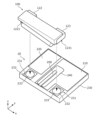
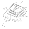
- FIG. 2 is a perspective view showing the configuration of the semiconductor laser device 1 according to this embodiment.
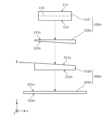
- FIG. 3 is a front view showing the configuration of the semiconductor laser device 1 according to this embodiment.
- the semiconductor laser device 1 includes a laser unit 20 and a lens section 100.
- the laser unit 20 includes a semiconductor laser element 200, a first bonding member 240, a submount 230, and a second bonding member 233.
- the submount 230 includes a base material 236, a first electrode 210, a second electrode 220, and two underlayers 232.
- the lens section 100 is fixed to the submount 230 by the second bonding member 233.
- the semiconductor laser device 1 is installed on the second stage 511b. The components of the semiconductor laser device 1 are described below.
- the submount 230 is a flat-shaped mounting base on which the semiconductor laser element 200 is attached.
- the submount 230 has a first upper surface 231, which is the upper surface of the flat plate shape.
- the first upper surface 231 is a plane parallel to the xy plane.
- a first electrode 210, a second electrode 220, and two underlayers 232 are arranged insulated from each other.
- the upper surface of the first electrode 210, the upper surface of the second electrode 220, and the upper surfaces of the two underlayers 232 are on the same plane, which is the first upper surface 231 of the submount.
- a first bonding member 240 is arranged above the first electrode 210.
- the semiconductor laser element 200 is installed above the first upper surface 231, more specifically, above the first bonding member 240.
- the base material 236 of the submount 230 is made of, for example, an insulating material such as crystals, such as AlN or SiC, or ceramic.
- the first electrode 210, the second electrode 220, and the two underlayers 232 are made of, for example, one or more metal films of metals, such as Ni, Cu, Pt, and Au.
- the first bonding member 240 is made of, for example, an inorganic material, such as a solder material, such as AuSn or SnAgCu.
- the first electrode 210 is electrically connected to the semiconductor laser element 200 by a metal wire (not shown).
- the first electrode 210 and the second electrode 220 are electrically connected to the lead pin 552 and supply power to the semiconductor laser element 200.
- the semiconductor laser element 200 is a laser element that includes a semiconductor laminate film and an optical waveguide formed on a semiconductor substrate.
- the semiconductor laminate film includes an active layer, that is, the semiconductor laser element 200 includes an active layer.
- the semiconductor laser element 200 is rectangular in shape, e.g., in the direction of the light guide.
- the width (width in the x-axis direction) of the semiconductor laser element 200 is, for example, 100 ⁇ m or more and 1 mm or less, and the length (length in the y-axis direction) is, for example, 500 ⁇ m or more and 10 mm or less.
- the width (width in the x-axis direction) of the optical waveguide is, for example, 5 ⁇ m or more and 500 ⁇ m or less, and it is a multi-transverse mode laser.
- the length (length in the y-axis direction) of the optical waveguide is the same value as the length of the semiconductor laser element 200.
- the region of the active layer included in the semiconductor laser element 200 that emits the laser light L1 is the light emitting region 201.
- the size of the light emitting region 201 is such that the width in the stacking direction of the semiconductor laminated film is the same value as the width of the active layer, and the width in the direction parallel to the stacking surface of the semiconductor laminated film is the same value as the width of the optical waveguide.
- the semiconductor laser element 200 emits laser light L1 having a predetermined wavelength and a predetermined divergence angle. More specifically, the semiconductor laser element 200 converts power input from the outside to the optical waveguide into stimulated emission light such as laser light L1, and emits it from the light-emitting region 201, which is one end of the optical waveguide.
- the fast axis of the laser light L1 is the axis in the stacking direction of the semiconductor laminated film of the semiconductor laser element 200.
- the slow axis which is perpendicular to the fast axis, is the axis parallel to the stacking surface of the semiconductor laminated film.
- the semiconductor laser element 200 can change the wavelength of the emitted laser light L1 depending on the semiconductor material of the semiconductor laser element 200. For example, by making the semiconductor laser element 200 a nitride-based semiconductor laser element mainly composed of nitrides of Al, Ga, and In, the semiconductor laser element 200 can emit laser light L1 having a peak wavelength of, for example, 350 nm or more and 550 nm or less. Also, by making the semiconductor laser element 200 a semiconductor laser element mainly composed of semiconductors composed of Al, Ga, In, As, and P, the semiconductor laser element 200 can emit laser light L1 having a peak wavelength of, for example, 600 nm or more and 1600 nm or less. Note that the semiconductor laser element 200 is not limited to semiconductor laser elements composed of the above semiconductor materials, and the wavelength of the laser light L1 emitted by the semiconductor laser element 200 is not limited to the above wavelength.
- Laser light L1 is emitted while spreading from light-emitting region 201.
- the width of light-emitting region 201 in the slow-axis direction (the direction parallel to the stacking surface of the semiconductor stacked film) is defined as width Ws. If the spread angle of emitted laser light L1 is defined as the angle width at which the value of the peak light intensity of laser light L1 is 1/( e2 ), the spread angle in the fast-axis direction is, for example, between 30° and 70°, and the spread angle in the slow-axis direction is, for example, between 3° and 25°.
- the optical waveguide of the semiconductor laser element 200 is disposed on the submount 230 side. That is, the semiconductor laser element 200 is fixed by so-called junction-down mounting.
- the active layer of the semiconductor laser element 200 is disposed so as to be parallel to the first upper surface 231 of the submount 230. That is, the active layer is parallel to the surface of the semiconductor laser element 200 on the submount 230 side.
- the first bonding member 240 between the submount 230 and the semiconductor laser element 200 can be configured to have a uniform thickness.
- the active layer is therefore a layer parallel to the xy plane, and the fast axis of the laser light L1 immediately after being emitted from the semiconductor laser element 200 is the z-axis direction, and the slow axis of the laser light L1 is an axis parallel to the x-axis direction.
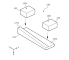
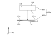
- FIG. 4 is an exploded perspective view of the lens unit 100 according to this embodiment.
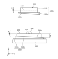
- FIG. 5 is a cross-sectional view showing a cut surface of the semiconductor laser device 1 taken along line V-V in FIG. 3.
- FIG. 5 shows only the semiconductor laser element 200, the submount 230, and the first cylindrical lens 110.
- FIG. 4 shows a state in which the x-axis and z-axis are inverted compared to FIG. 2. Also, in FIG. 4, the installation direction, etc. are shown with dashed arrows.
- the first cylindrical lens 110 receives the laser light L1 emitted from the semiconductor laser element 200 and emits the laser light L1 with a small divergence angle in the fast axis direction.
- the divergence angle in the fast axis direction of the laser light L1 emitted from the first cylindrical lens 110 is, for example, between -1° and +1°. An angle with a negative sign indicates convergence.
- the laser light L1 emitted from the semiconductor laser element 200 is directly incident on the first cylindrical lens 110.
- the first cylindrical lens 110 is a lens that pseudo-collimates the laser light L1 in the fast axis direction.
- the first cylindrical lens 110 is an optical component having a power axis having power (refractive power) and a non-power axis. Furthermore, the power axis and the non-power axis are arranged in a perpendicular relationship. That is, the first cylindrical lens 110 has a cylindrical surface.
- the first cylindrical lens 110 has a cylindrical surface that is convexly curved on the power axis, that is, the surface of a convex cylinder.
- the first cylindrical lens 110 is a convex cylindrical lens.
- the first cylindrical lens 110 is a convex lens.
- the power axis is inclined with respect to the fast axis of the laser light L1.
- the first cylindrical lens 110 has an entrance surface 117 where the laser light L1 is incident and an exit surface 116 where the laser light is emitted.
- the first cylindrical lens 110 is a plano-convex cylindrical lens with a flat entrance surface and a convex exit surface.
- the entrance surface 117 is a surface parallel to the zx plane.
- the exit surface 116 is a first cylindrical surface, which is a convex surface whose curved surface is expressed by a spherical function or an aspherical function.
- the power axis is an axis parallel to the zx plane and is inclined with respect to the z axis.
- a plano-convex cylindrical lens is used as the first cylindrical lens 110, but a biconvex cylindrical lens, such as a convex meniscus cylindrical lens with one side convex and the other concave, may also be used.
- the first cylindrical lens 110 is a member made of an inorganic transparent material such as glass, and an anti-reflection coating film that matches the wavelength of the laser light L1 is formed on the entrance surface 117 and exit surface 116 of the laser light L1.
- the support member 120 is a member that is joined to the first cylindrical lens 110 and supports the first cylindrical lens 110.
- the support member 120 includes a first support member 121, a second support member 122, and a third support member 123.
- the first support member 121 is a member including a plate-like portion including a lower surface 1212 parallel to the xy plane, and a slope portion including a lower surface 1211 inclined with respect to the xy plane.
- the lower surface 1211 is a surface inclined in the x-axis direction from the xy plane, in other words, a surface inclined in a direction rotated around the y axis from the xy plane.
- the second support member 122 and the third support member 123 have a rectangular parallelepiped shape, and are joined to the lower surface 1212 of the first support member 121 at the surface on the positive side of the z axis of the rectangular parallelepiped shape.
- the second support member 122 includes a lower surface 1221, which is a surface facing away from the surface joined to the lower surface 1212 and is a surface on the negative side of the z axis of the rectangular parallelepiped shape.
- the third support member 123 includes a lower surface 1231, which is a surface facing away from the surface joined to the lower surface 1212 and is a surface on the negative side of the z axis of the rectangular parallelepiped shape.
- the lower surface 1221 and the lower surface 1231 are parallel to the xy plane and are located on the same plane.
- the lower surface 1221 and the lower surface 1231 are planes on which the lens unit 100 is bonded to a flat surface (first flat surface), and are called the installation plane.
- the installation plane in this embodiment is the lower surface 1221 of the second support member 122 and the lower surface 1231 of the third support member 123.
- the first cylindrical lens 110 is bonded to the lower surface 1211. Therefore, the first cylindrical lens 110 is bonded to the support member 120 in a state inclined from the xy plane.
- the support member 120 includes a bonding surface, which is the surface where the support member 120 is bonded to the first cylindrical lens 110.
- the lower surface 1211 of the slope portion included in the first support member 121 is the bonding surface.
- the first support member 121, the second support member 122, and the third support member 123 are formed by processing a substrate of a semiconductor material such as glass or silicon by partial etching, polishing, cutting, etc. They may also be formed of a metal such as Fe or an Fe alloy, or a ceramic such as Al2O3 , ZrO2 , Si3N4 , or AlN.
- the first cylindrical lens 110, the first support member 121, the second support member 122, and the third support member 123 are bonded to each other by a direct bonding method such as optical contact.
- the first cylindrical lens 110, the first support member 121, the second support member 122, and the third support member 123 are bonded to each other via a bonding material such as low-melting point glass.
- a solder material such as AuSn solder may be used as the bonding material.
- the installation plane is an example of the first installation plane.
- an installation plane described without an ordinal number means the first installation plane.
- the installation plane is a plane that is joined to the installation plane (lower surface 1221 and lower surface 1231) of the lens unit 100 and to which the lens unit 100 is fixed.
- the installation plane is a plane provided on the light source module 10, and in this case, a plane provided on the semiconductor laser device 1.
- the installation plane is the first upper surface 231 of the submount 230.
- the installation plane (first upper surface 231) is fixed to the support member 120 of the lens unit 100. More specifically, the installation plane (first upper surface 231) is fixed to the lower surface 1221 of the second support member 122 and the lower surface 1231 of the third support member 123 included in the support member 120.
- the support member 120 is a member that is fixed to the flat surface on which it is to be placed (first upper surface 231), and is also a member that is joined to the first cylindrical lens 110.
- the first cylindrical lens 110 is joined to the flat surface on which it is to be placed (first upper surface 231) via the support member 120.
- busbar 115 of the first cylindrical lens 110 will be described.
- the first cylindrical lens 110 is a cylindrical lens having a first cylindrical surface.
- the first cylindrical surface has a generating line 115 illustrated by a dashed line.
- the emission surface 116 of the first cylindrical lens 110 is a convex first cylindrical surface.
- a generating line is a straight line at each position when the cylindrical surface (curved surface) of the first cylindrical surface is created by linear movement (when drawn by linear movement), and the generating line 115 is one of countless generating lines.
- the generating line 115 is a straight line along the convex apex part of the surface of the convex cylinder that is the emission surface 116.
- the generating line 115 of the first cylindrical lens 110 in this embodiment is inclined with respect to the installation plane (first upper surface 231).
- the generating line 115 is also inclined with respect to the installation plane (lower surface 1221 and lower surface 1231) of the lens unit 100. Since the mounting plane (first upper surface 231), the active layer, and the xy plane are parallel, the busbar 115 is inclined with respect to the active layer and the xy plane of the semiconductor laser element 200. In addition, the mounting plane (lower surface 1221 and lower surface 1231), the active layer, and the xy plane are parallel to each other.
- the angle between the busbar 115 and the active layer is defined as angle ⁇ .
- ⁇ the angle between the busbar 115 and the active layer.
- the busbar 115 is inclined clockwise with respect to the mounting plane (first upper surface 231) and the xy plane when viewed from the front.
- the angle ⁇ between the busbar 115 and the mounting plane is equal to ⁇ .
- the angle ⁇ between the active layer and the mounting plane is 0°.
- the components of the light source module 10 will be described again with reference to FIG. 1.
- semiconductor laser device 1 (more specifically, semiconductor laser element 200) emits laser light L1.
- semiconductor laser devices 2 to 6 emit laser light L2, L3, L4, L5, and L6, respectively.
- the multiple laser lights i.e., laser light L1 to L6 emitted from the multiple semiconductor laser devices are incident on a slow axis collimator lens 600 (hereinafter referred to as SAC lens 600).
- the SAC lens 600 is a lens that has a convex cylindrical surface.
- the SAC lens 600 is made of glass with an anti-reflection coating film formed on the surface, and in this embodiment, it is a plano-convex cylindrical lens. Note that in this embodiment, a plano-convex cylindrical lens is used as the SAC lens 600, but a biconvex cylindrical lens or a convex meniscus cylindrical lens with one side convex and the other concave may also be used. A concave reflective cylindrical mirror may also be used as the SAC lens 600.
- the SAC lens 600 has a cylindrical surface that is convexly curved in the power axis, i.e., a convex cylindrical surface.
- the SAC lens 600 has a non-power axis in a direction perpendicular to the power axis.
- the SAC lens 600 is a lens that has power in the slow axis of the laser light.
- Each of the multiple SAC lenses 600 collimates the component of the laser light that is incident in the slow axis direction.
- the laser light emitted from the multiple semiconductor laser devices and passing through the multiple SAC lenses 600 travels as collimated emitted light in both the fast axis and the slow axis.
- Each of the multiple SAC lenses 600 is installed in the first stage of each of the multiple stages.
- the SAC lens 600 into which the laser light L1 is incident is installed in the first stage 511a.
- a reflecting mirror 700 is arranged in the direction in which the laser light from each of the multiple semiconductor laser devices is emitted.
- Each of the multiple reflecting mirrors 700 is an optical component having an incident surface onto which the laser light that has passed through each of the multiple SAC lenses 600 is incident.
- the multiple reflecting mirrors 700 each reflect the laser light collimated by the multiple first cylindrical lenses 110 and the multiple SAC lenses 600 described above, and deflect the direction of the laser light by 90°.
- Each of the multiple reflecting mirrors 700 is installed on the first stage of each of the multiple stages. For example, the reflecting mirror 700 on which the laser light L1 is incident is installed on the first stage 511a.
- the multiple laser beams, each reflected by the reflecting mirror 700, are spatially combined so that they have the same optical axis in the fast axis, i.e., the z-axis direction, when each laser beam is emitted from the semiconductor laser element 200, and reach the focusing lens 800 fixed to the base 502.
- the focusing lens 800 is an optical component having an entrance surface on which the laser light that has passed through each of the multiple SAC lenses 600 is incident. Furthermore, the focusing lens 800 is also an optical component on which the multiple laser light that has passed through the reflecting mirror 700 is incident. In this embodiment, the focusing lens 800 is a lens that focuses the multiple laser light that has arrived. Multiple parallel laser light beams, each of which has the same optical axis as the fast axis due to the reflecting mirror 700, are incident on the focusing lens 800. Furthermore, the multiple laser light beams focused by the focusing lens 800 are incident on the entrance surface, which is the end face of the core 550a of the optical fiber 550, which is an example of the target object.
- the multiple laser light beams can be efficiently focused on the end face of the core 550a, which is the target object.
- the laser light beams emitted from the multiple semiconductor laser devices that have been focused by the reflecting mirror 700 are coupled to the optical fiber 550 and the core 550a.
- the optical fiber 550 penetrates the side wall 503. Therefore, the laser light coupled to the optical fiber 550 is guided to the outside of the light source module 10.
- the boot 551 is a member that covers and protects the periphery of the optical fiber 550.
- the multiple SAC lenses 600 corresponding to the multiple semiconductor laser devices can all be of the same shape, and the multiple reflecting mirrors 700 corresponding to the multiple semiconductor laser devices can all be of the same shape.
- one semiconductor laser device, one SAC lens 600, and one reflecting mirror 700 are arranged on each of the multiple stages of the staircase base 510.
- first cylindrical lens 110 will be described in more detail using Figures 5 and 6.
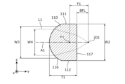
- FIG. 6 is an enlarged cross-sectional view of the light-emitting region 201 and the first cylindrical lens 110 in FIG. 5.
- a cross-sectional view is a view showing only the surface that appears in the cross section.
- the optical axis A1 of the laser light L1 may be shown by a dashed line. Note that in FIG. 6, the light-emitting region 201 is shown as a dot for the sake of explanation.
- the first cylindrical lens 110 in this embodiment is a member having an entrance surface 117, an exit surface 116, a first side surface 111, and a second side surface 112.
- the laser light L1 is emitted from the light emitting region 201 of the semiconductor laser element 200, and then enters the incident surface 117 of the first cylindrical lens 110. Furthermore, the laser light L1 incident from the incident surface 117 is emitted from the exit surface 116. The laser light L1 emitted from the exit surface is pseudo-collimated light.
- the first side 111 is a side parallel to the generating line 115.
- the second side 112 is a side facing away from the first side 111 and parallel to the generating line 115.
- the first side 111 is located on the positive side of the z-axis, so it can also be said to be the upper surface of the first cylindrical lens 110, and the second side 112 is located on the negative side of the z-axis, so it can also be said to be the lower surface of the first cylindrical lens 110.
- the lower surface 1211 of the slope portion included in the first support member 121 is the joint surface.
- the joint surface (lower surface 1211) is joined to the first side surface 111 or the second side surface 112, but here it is joined to the first side surface 111.
- the joint surface (lower surface 1211) is a surface parallel to the first side surface 111, the second side surface 112, and the busbar 115.
- the first cylindrical lens 110 will be described in detail with reference to FIG. 6.
- the first cylindrical lens 110 is defined as follows:
- the dimensions of the first cylindrical lens 110 are thickness T1 in the y-axis direction and width W2 in the z-axis direction.
- the refractive index of the first cylindrical lens 110 is n.
- the position of the principal point of the first cylindrical lens 110 is principal point P1
- the effective focal length is effective focal length F1
- the distance from the focal position to the incident surface 117 is distance BFL.
- the effective aperture width on the emission side of the laser light L1 is effective aperture width W3.
- the light emitting region 201 of the semiconductor laser element 200 is disposed at the focal position, and the distance between the principal point P1 and the light emitting region 201 is the effective focal length F1.
- the laser light L1 emitted from the light emitting region 201 at a predetermined spread angle is pseudo-collimated by the first cylindrical lens 110, and becomes the laser light L1 with a beam width W4 in the fast axis direction.
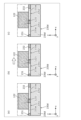
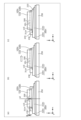
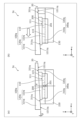
- FIGS. 7, 8, 9, 10, and 11 are schematic diagrams showing steps in a manufacturing method for the semiconductor laser device 1 of the light source module 10 according to this embodiment. Note that in the drawings showing the manufacturing method below, the installation direction, etc. may be indicated by dashed arrows. Also, in FIG. 7 to FIG. 9, the x-axis and z-axis are shown inverted compared to FIG. 2.
- the semiconductor laser device 1 is manufactured in the following order, as shown in Figures 7 to 11.
- a preparation step is carried out.
- the lens section 100 and the laser unit 20 are manufactured and prepared.
- the support member 120 is manufactured.
- the second support member 122 and the third support member 123 are joined to the first support member 121. More specifically, the upper surface of the second support member 122 (the surface facing away from the lower surface 1221) and the upper surface of the third support member 123 (the surface facing away from the lower surface 1231) are each joined to the lower surface 1212 of the first support member 121.
- the first cylindrical lens 110 is bonded to the support member 120. More specifically, the first side surface 111 of the first cylindrical lens 110 is bonded to the lower surface 1211 of the slope portion included in the first support member 121 of the support member 120. In other words, the first cylindrical lens 110 is bonded to the bonding surface (lower surface 1211) of the first support member 121. This fixes the positional relationship between the first cylindrical lens 110, the first support member 121, the second support member 122, and the third support member 123, and the lens unit 100 is manufactured.
- the laser unit 20 is manufactured before the lens section 100 is placed on the flat surface.
- two underlayers 232 are formed in advance on the first upper surface 231 side of the base material 236.
- the two underlayers 232 are formed by patterning the same metal material into a rectangular shape when forming the first electrode 210 and the second electrode 220, and are spaced apart from the first electrode 210 on which the semiconductor laser element 200 is placed. Therefore, the first upper surface 231, which is the flat surface on which the laser unit 200 is placed, becomes the surface (upper surface) of the first electrode 210, the second electrode 220, and the underlayer 232, which are the same plane.
- first bonding member 240 and two second bonding members 233 are pre-layered on the submount 230.
- the two second bonding members 233 are layers laminated on the base layer 232, and in this case are solder layers made of a solder material.
- the two second bonding members 233 have a circular shape, and are layers for bonding the first upper surface 231 of the submount 230 and the lens section 100 (more specifically, the support member 120).
- the semiconductor laser element 200 is bonded to a predetermined position on the first bonding member 240 of the submount 230 by the first bonding member 240.
- the submount 230 is placed on a heating stage, and the semiconductor laser element 200 is placed on the first bonding member 240 and pressurized.
- the first bonding member 240 is then heated to above its melting point by the heating stage, and then cooled. This bonds the submount 230 and the semiconductor laser element 200, and the laser unit 20 is manufactured.
- the laser unit 20 is fixed onto the second step 511b of the staircase base 510 of the case 501.
- the laser unit 20 is fixed to the staircase base 510 by a bonding material (not shown).
- the optical fiber 550, the focusing lens 800, and the reflecting mirror 700 are fixed to the case 501 in predetermined positions.
- the placement step is performed.
- the lens section 100 is placed at a predetermined position on the laser unit 20. More specifically, the lens section 100 is placed on the first upper surface 231 of the submount 230, which is the flat surface on which the lens section 100 is to be placed.
- the lens section 100 is placed so that the laser light L1 emitted from the semiconductor laser element 200 is incident on the first cylindrical lens 110 and the generating line 115 of the first cylindrical lens 110 is inclined with respect to the flat surface on which the lens section 100 is to be placed (the first upper surface 231).
- the lens unit 100 is arranged so that, with the lens unit 100 shown in FIG. 9 turned upside down, one second joining member 233 contacts the lower surface 1221 of the second support member 122, and the other second joining member 233 contacts the lower surface 1231 of the third support member 123.
- the lens unit 100 is arranged so that the laser light L1 is incident on the first cylindrical lens 110, and the generatrix 115 is inclined with respect to the installation plane (first upper surface 231).
- the lens section 100 and the laser unit 20 are not joined together, meaning that the relative positions of the lens section 100 and the submount 230 are not fixed.
- the lens section 100 can be moved relative to the position of the submount 230.
- the SAC lens 600 is also placed in a predetermined position in the case 501, but like the lens unit 100, it is not fixed to the case 501.
- the alignment step is a process of moving the lens unit 100 arranged in the arrangement step.
- the alignment step is also a process of making the laser light L1 emitted from the semiconductor laser element 200 enter the first cylindrical lens 110.
- the alignment step is a process of moving the lens unit 100 in two mutually orthogonal directions parallel to the installation plane (first upper surface 231).
- the installation plane (first upper surface 231) is parallel to the xy plane, the lens unit 100 can be moved in the x-axis direction and the y-axis direction.
- the lens unit 100 can be moved along the installation plane (first upper surface 231), and here, the installation plane (lower surface 1221 and lower surface 1231) of the lens unit 100 moves relative to the installation plane (first upper surface 231).
- the generatrix 115 of the first cylindrical lens 110 moves in the z-axis direction at a specific position in the x-axis direction because it is inclined with respect to the x-axis.
- the z-axis deviation d between the generatrix 115 of the first cylindrical lens 110 and the laser light L1 that has reached the first cylindrical lens 110 changes.
- the distance from the z-axis position of the optical axis of the laser light L1 that has reached the first cylindrical lens 110 to the z-axis position of the generatrix of the first cylindrical lens 110 is defined as the z-axis deviation d at the position of the optical axis of the laser light L1 that has reached the first cylindrical lens 110.
- the angle of the traveling direction of the laser light L1 emitted from the first cylindrical lens 110 can be changed in the fast axis direction (z-axis direction).
- the angle between the optical axis A1 of the laser light L1 and the optical axis (not shown) of the optical system of the light source module 10 can be controlled.
- the optical system of the light source module 10 is arranged as designed, as shown in FIG. 5, by setting the z-axis deviation d to zero, the optical axis A1 of the emitted laser light L1 becomes parallel to the optical axis of the optical system of the light source module 10.
- the coupling efficiency between the laser light L1 and the core 550a at the end face of the optical fiber 550 can be increased.
- the coupling efficiency may be referred to as the coupling efficiency of the laser light L1 or simply as the coupling efficiency.
- the lens unit 100 when the lens unit 100 is moved in the y-axis direction, the distance between the incident surface 117 of the first cylindrical lens 110 and the light-emitting region 201 is changed. As a result, the parallelism of the laser light L1 emitted from the first cylindrical lens 110 can be controlled. As a result, the coupling efficiency between the laser light L1 and the core 550a can be further improved.
- a device such as a collet comes into contact with the support member 120, thereby moving the lens unit 100.
- the collet does not come into direct contact with the first cylindrical lens 110.
- the lens unit 100 can be moved as a unit. In other words, the entire lens unit 100 can be moved while the positional relationship between the first cylindrical lens 110, the first support member 121, the second support member 122, and the third support member 123 is fixed.
- the position of the lens unit 100 is moved, that is, the position of the lens unit 100 is adjusted, so as to increase the coupling efficiency between the emitted laser light L1 and the optical fiber 550.
- the lens unit 100 may be moved while the semiconductor laser element 200 emits the laser light L1.
- the laser light L1 emitted from the semiconductor laser element 200 passes through the first cylindrical lens 110, the SAC 600, the reflecting mirror 700, and the focusing lens 800 and is focused on the end face of the optical fiber 550.
- the position of the lens unit 100 is adjusted while observing the light intensity of the laser light L1 emitted from the optical fiber 550. Specifically, the lens unit 100 is slightly moved in the x-axis and y-axis directions. At this time, the position of the lens unit 100 is adjusted so that the light intensity of the laser light L1 emitted from the optical fiber 550 is maximized, which is known as active alignment.
- the fixing step is a process of fixing the lens unit 100, which has been moved in the alignment step, to the installation plane (first upper surface 231).
- the solder material constituting the second joining members 233 melts, and the lens unit 100 and the flat surface (first upper surface 231) are fixed together.
- the semiconductor laser device 1 shown in FIG. 11 is manufactured.
- the lens unit 100 (more specifically, the support member 120) and the submount 230 are bonded at the installation plane (lower surface 1221 and lower surface 1231) and the installation surface (first upper surface 231).
- the bonding area can be made larger than when the lens unit 100 and the submount 230 are bonded at points, and this allows the thickness of the two second bonding members 233 to be made thinner.
- the thickness of the two second bonding members 233 is 0 ⁇ m or more and 10 ⁇ m or less. Note that a thickness of 0 ⁇ m for the second bonding member 233 means that there is a point where the installation plane and the installation surface are partially in contact.
- the method for manufacturing the light source module 10 includes a placement step, an alignment step, and a fixing step.
- the alignment step is a process of moving the lens unit 100, that is, the first cylindrical lens 110.
- the first cylindrical lens 110 in this embodiment is a position adjustment lens whose position can be adjusted to optimize the optical axis and parallelism of the laser light L1 in the semiconductor laser device 1.
- the generatrix 115 of the first cylindrical lens 110 is inclined with respect to the mounting plane (first upper surface 231), and is also inclined with respect to the active layer of the semiconductor laser element 200.
- the effect of the angle ⁇ between the generatrix 115 and the mounting plane (first upper surface 231) on alignment will be described below.
- FIG. 12 is a diagram showing the relationship between the angle ⁇ in this embodiment and the amount of movement ( ⁇ z) in the z-axis direction and the amount of movement ( ⁇ x) in the x-axis direction of the first cylindrical lens 110.
- the amount of movement in the z-axis direction may be written as ⁇ z
- the amount of movement in the x-axis direction as ⁇ x.
- the horizontal axis is the angle ⁇
- the vertical axis is the value obtained by dividing ⁇ z of the first cylindrical lens 110 by ⁇ x of the first cylindrical lens 110.
- FIG. 13 is a front view showing an example in which the lens unit 100 (first cylindrical lens 110) has moved in the x-axis direction in the alignment step according to this embodiment. More specifically, FIG. 13(a) is a front view before the lens unit 100 (first cylindrical lens 110) has moved, and FIG. 13(b) is a front view after the lens unit 100 (first cylindrical lens 110) has moved. For simplicity, FIG. 13 mainly shows the first cylindrical lens 110 and the semiconductor laser element 200.
- the case where the first cylindrical lens 110 moves from the position in FIG. 13(a) to the position in FIG. 13(b) in the alignment step will be described.
- the amount of movement in the x-axis direction from the position in FIG. 13(a) to the position in FIG. 13(b) is ⁇ x.
- the case where the position of the optical axis of the laser light L1 that reaches the first cylindrical lens 110 coincides with the center position of the light-emitting region 201 is shown here.
- the z-axis direction deviation d between the light-emitting region 201 and the bus line 115 changes from d1 shown in FIG. 13(a) to d2 shown in FIG. 13(b).
- the ⁇ x of the first cylindrical lens 110 shown in FIG. 12 indicates the amount of change in the movement of the first cylindrical lens 110 in the x-axis direction in the above alignment step.
- the ⁇ z of the first cylindrical lens 110 indicates the amount of change in the z-axis direction deviation d between the light emitting area 201 and the generating line 115 in a front view when the first cylindrical lens 110 moves in the x-axis direction.
- the vertical axis in FIG. 12 is 0.1, and the position in the z-axis direction can be adjusted with an accuracy 10 times the equipment accuracy.
- FIG. 14 is a diagram showing the relationship between angle ⁇ , ⁇ z, and ⁇ x in this embodiment.
- the z-axis misalignment d between the bus bar 115 and the light-emitting region 201 changes.
- the movement of the first cylindrical lens 110 in the x-axis direction can be converted into the movement of the first cylindrical lens 110 in the z-axis direction.
- ⁇ z/ ⁇ x is less than 1
- the amount of change in position in the z-axis direction can be made gentler than the amount of change in position in the x-axis direction.
- ⁇ ⁇ , 0° ⁇
- the following control may be performed.
- the position of the lens unit 100 may be changed within a range of ⁇ 57 ⁇ m in the x-axis direction.
- the position of the lens unit 100 may be changed within a range of ⁇ 9.5 ⁇ m in the x-axis direction.
- the lens unit 100 may be moved by a larger amount in the x-axis direction.
- the effect is that the position of the first cylindrical lens 110 (more specifically, the busbar 115) in the z-axis direction can be adjusted more easily. It is even better if ⁇ z/ ⁇ x is 0.01 or more, and 0.5° ⁇
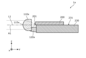
- the semiconductor laser device 1x has the same configuration as the semiconductor laser device 1, except that it has a fast axis collimator lens (hereinafter, FAC lens) 110x instead of the first cylindrical lens 110, and a bonding material 120x made of solder or the like instead of the support member 120.
- FAC lens fast axis collimator lens
- the generatrix 115x is parallel to the installation plane (first upper surface 231) and the active layer.
- the FAC lens 110x is bonded to the submount 230 by the bonding material 120x.
- the light source module according to the comparative example has the same configuration as the light source module 10 according to the present embodiment, except that it has six semiconductor laser devices 1x instead of the semiconductor laser devices 1 to 6.
- FIG. 16 is a diagram showing the relationship between the change in the position in the z-axis direction of the FAC lens 110x in a light source module including a semiconductor laser device 1x according to a comparative example, and the coupling efficiency of the laser light to the optical fiber 550.
- FIG. 16 shows the results of calculations performed by simulation of the coupling efficiency under three different conditions (No. 1, No. 2, No. 3) in the semiconductor laser device 1x.
- FIG. 17 shows a table explaining the simulation conditions of FIG. 16.
- the width Ws of the light emitting region 201 of the semiconductor laser element 200 In order to increase the optical output of the light emitted from the light source module 10, it is necessary to increase the width Ws of the light emitting region 201 of the semiconductor laser element 200 and increase the optical output. Also, in order to increase the radiance of the light emitted from the light source module 10, it is necessary to reduce the core diameter (diameter) of the core 550a of the optical fiber 550.
- the coupling efficiency of the laser light to the optical fiber 550 is strongly dependent on the width Ws of the light emitting region 201 of the semiconductor laser element 200 and the core diameter (diameter) of the core 550a of the optical fiber 550.
- the effective focal length F1 and distance BFL of the FAC lens 110x are 0.38 mm and 0.09 mm
- the effective focal length of the SAC lens 600 is 13.5 mm
- the effective focal length of the condenser lens 800 is 7.3 mm
- the combination of the width Ws and the core diameter of the core 550a is changed.
- the peak wavelength of the semiconductor laser element 200 is 450 nm
- the numerical aperture NA of the optical fiber 550 is 0.22.
- Ws was 50 ⁇ m and the core diameter was 50 ⁇ m.
- Ws was 50 ⁇ m and the core diameter was 70 ⁇ m.
- Ws was 100 ⁇ m and the core diameter was 100 ⁇ m.
- Figure 16 shows the change in coupling efficiency when all six FAC lenses 110x are moved the same amount in the positive z-axis direction or the negative z-axis direction from the position in the z-axis direction of 0.
- the angle between the optical axis A1 of the laser light L1 and the optical axis of the semiconductor laser element 200 changes in the positive direction of the z-axis, so that the position of the laser light L1 on the incident surface of the core 550a of the optical fiber 550 is shifted in the positive direction of the z-axis, and the coupling efficiency decreases.
- the coupling efficiency decreases to about 0.4.
- the distance BFL is 0.09 mm, which is very large. Therefore, the thickness of the bonding material 120x in the y-axis direction is about 0.09 mm, which is very large compared to the misalignment amount of several ⁇ m that affects the coupling efficiency described above.
- the bonding material 120x in the manufacturing process of bonding the FAC lens 110x and the submount 230, when the bonding material 120x is melted, the bonding material 120x may sag in the negative z-axis direction due to gravity, for example, and the distribution of the bonding material 120x may change in the z-axis direction.
- the bonding material 120x is attached to the lower part (surface on the negative z-axis side) of the FAC lens 110x.
- the bonding material 120x in the y-axis direction is very thick and there is a distribution in the thickness in the z-axis direction, when the bonding material 120x melts and then hardens, the bonding material 120x may easily shrink by about several ⁇ m in the z-axis direction. In this way, because the bonding material 120x sags and the amount of shrinkage is large, the position of the FAC lens 110x according to the comparative example is shifted in the z-axis direction from the designed position.
- the incident position of the laser light L1 at the end face of the optical fiber 550 is shifted from the center of the core 550a, and the coupling efficiency decreases.
- the actual distance BFL is shifted from the designed value of 0.09 mm, the parallelism of the laser light L1 deteriorates, and the major axis and minor axis (size) of the laser light L1 at the incident surface of the optical fiber 550 increase.
- the major axis of the laser light L1 at the incident surface of the optical fiber 550 becomes larger than the core diameter of the optical fiber 550, the coupling efficiency decreases.
- the thickness of the two second bonding members 233 that bond the lens unit 100 (more specifically, the support member 120) and the submount 230 can be about 0.1 ⁇ m or more and 10 ⁇ m or less, that is, can be made sufficiently thin. Therefore, the amount of shrinkage when the second bonding members 233 melt and then harden is smaller than the amount of shrinkage of the bonding material 120x in the comparative example. Furthermore, as an example, if the z-axis direction is the vertical direction, that is, the xy plane is parallel to the horizontal direction, the two second bonding members 233 are prevented from sagging in the negative z-axis direction when melted. In this way, because the amount of shrinkage is small and the second bonding members 233 are less likely to sag, the coupling efficiency in the light source module 10 including the semiconductor laser device 1 in this embodiment is less likely to decrease.
- the busbar 115 is tilted with respect to the active layer, aberration occurs. Therefore, it is expected that distortion will occur in the light intensity distribution of the laser beams L1 to L6 at the incident surface of the focusing lens 800 and in the light intensity distribution of the laser beams L1 to L6 at the incident surface of the optical fiber 550.
- FIG. 18 shows the results of a simulation calculation of the light intensity distribution when the angle ⁇ is 0° and the angle ⁇ is 2° in this embodiment. More specifically, FIG. 18(a) shows the light intensity distribution of the laser beams L1 to L6 at the incident surface of the focusing lens 800, and FIG. 18(b) shows the light intensity distribution of the laser beams L1 to L6 at the incident surface of the optical fiber 550. The outline of the target core 550a is also shown by a dashed line. FIG. 18 shows the beam spots of the laser beams L1 to L6, with the darker areas indicating higher light intensity.
- the light intensity distribution is calculated under the conditions that the width Ws of the light-emitting region 201 is 50 ⁇ m, the core diameter D is 50 ⁇ m, and the angle ⁇ is 2°.
- the beam spots of the laser beams L1 to L6 each have a shape that rises to the right.
- the laser beams L1 to L6 are focused by the focusing lens 800, and the laser beams L1 to L6 form a single beam spot on the incident surface of the optical fiber 550.
- This single beam spot rises to the right, just like FIG. 18(a), and its major axis exceeds the core diameter D of the optical fiber 550. Therefore, some of the laser beams L1 to L6 are focused outside the core 550a, but most of the laser beams L1 to L6 are focused in the core 550a. In other words, the laser beams L1 to L6 are coupled to the core 550a.
- FIG. 19A is a diagram showing the results of a simulation calculation of the change in coupling efficiency when the first cylindrical lens 110 according to this embodiment is moved along the installation plane in a semiconductor laser device 1 in which the first cylindrical lens 110 according to this embodiment is inclined relative to the installation plane.
- FIG. 19B is a diagram showing the results of a simulation calculation of the maximum value of coupling efficiency when the angles ⁇ and ⁇ according to this embodiment are changed.
- the light source module used is one with the condition No. 1 in FIG. 17. That is, the width Ws of the light emitting region 201 is 50 ⁇ m and the core diameter D is 50 ⁇ m.
- FIG. 19A shows the change in coupling efficiency when the first cylindrical lens 110 is moved in the x-axis direction when the angle ⁇ in this embodiment is greater than 0, specifically when the angle ⁇ is 0.5°, 1°, and 2°.
- the coupling efficiency is about 0.4 at the adjustment start position, that is, when the movement amount is 0 ⁇ m, but the coupling efficiency improves by moving in the positive x-axis direction.
- the angle ⁇ is 2°, the coupling efficiency is restored to 0.7 by moving about 29 ⁇ m in the positive x-axis direction.
- the coupling efficiency is restored to 0.9 or more by moving about 57 ⁇ m in the positive x-axis direction. Furthermore, when the angle ⁇ is 0.5°, the coupling efficiency is restored to about 0.98 by moving about 120 ⁇ m in the positive x-axis direction.
- the angle ⁇ greater than 0° and moving the lens unit 100 (first cylindrical lens 110) in the x-axis direction, the z-axis deviation d between the generating line 115 and the light-emitting region 201 can be changed, thereby improving the coupling efficiency.
- the range in the x-axis direction in which the coupling efficiency is 90% of the maximum value from the point where the coupling efficiency is maximized at each angle is ⁇ 10 ⁇ m or more when the angle ⁇ is 2°, ⁇ 20 ⁇ m or more when the angle ⁇ is 1°, and ⁇ 30 ⁇ m or more when the angle ⁇ is 0.5°.
- the movement of the first cylindrical lens 110 in the x-axis direction is converted into the movement of the first cylindrical lens 110 in the z-axis direction, and ⁇ z/ ⁇ x can be reduced. Therefore, even if the lens unit 100 moves unintentionally, the amount of change in the position of the first cylindrical lens 110 in the z-axis direction can be made gentle.
- the amount of decrease in coupling efficiency can be reduced compared to the FAC lens 110x of the light source module of the comparative example shown in FIG. 17.
- the maximum coupling efficiency is calculated under the following conditions: the width Ws of the light-emitting region 201 is 50 ⁇ m and the core diameter D is 50 ⁇ m; the width Ws of the light-emitting region 201 is 50 ⁇ m and the core diameter D is 70 ⁇ m; and the width Ws of the light-emitting region 201 is 100 ⁇ m and the core diameter D is 100 ⁇ m.
- the coupling efficiency decreases. However, if the angle ⁇ is in the range of 0° to 2°, the coupling efficiency is approximately 0.7 to 0.9. On the other hand, in the comparative example shown in FIG. 17, the coupling efficiency drops sharply to 0.4 or less when the FAC lens 110x is shifted from the optimal position in the negative z-axis direction by just a few ⁇ m.
- an optimal angle ⁇ for example, by setting the angle ⁇ between 0.5° and 2°, a semiconductor laser device 1 that exhibits high coupling efficiency can be realized.
- the manufacturing method for the light source module 10 according to this embodiment is as follows.
- a case 501 is prepared.
- a staircase base 510, a condenser lens 800, an optical fiber 550, and a boot 551 are placed inside the case 501.
- a plurality of semiconductor laser devices 1 to 6 are fixed onto the staircase base 510.
- a plurality of slow axis collimator lenses 600 (SAC lenses 600) and a plurality of reflecting mirrors 700 are temporarily placed onto the staircase base 510.
- Semiconductor laser devices 1 to 6 are wired and connected via lead pins 552. While semiconductor laser devices 1 to 6 are driven, the x-axis and y-axis positions of SAC lens 600 and reflecting mirror 700 are moved and fixed while being adjusted so that the amount of light incident on optical fiber 550 is maximized (so that coupling efficiency is maximized) (in other words, active alignment is performed). After the lid of case 501 is closed, case 501 is sealed. With this general manufacturing method, all mounting surfaces are parallel to the xy plane, and height and angle adjustments in the z-axis direction are not performed, so the optical precision of each component directly contributes to the coupling efficiency.
- Fig. 20 is a front view showing a configuration of a semiconductor laser device 1a according to Modification 1 of Embodiment 1. More specifically, Fig. 20(a) is a front view before a lens unit 100a included in the semiconductor laser device 1a is moved, and Fig. 20(b) is a front view after the lens unit 100a is moved.
- the semiconductor laser device 1a according to this modified example has the same configuration as the semiconductor laser device 1 according to the first embodiment, except that it has a lens unit 100a instead of the lens unit 100, and further has a fixing member 300.
- the lens unit 100a is a member having a support member 120a and a first cylindrical lens 110.
- the support member 120a is composed of a first support member 121 according to the first embodiment.
- the fixing member 300 is a member having a third upper surface which is a flat surface on which the lens unit 100a is fixed.
- the fixing member 300 is a member having a first fixing member 310 and a second fixing member 320.
- the first fixing member 310 and the second fixing member 320 have a rectangular parallelepiped shape, and here have the same shape as each other.
- the first fixing member 310 includes an upper surface 311 which is the surface on the positive side of the z-axis of the rectangular parallelepiped shape.
- the second fixing member 320 includes an upper surface 321 which is the surface on the positive side of the z-axis of the rectangular parallelepiped shape.
- the upper surfaces 311 and 321 are parallel to the xy plane and are located on the same plane.
- the upper surface 311 of the first fixing member 310 and the upper surface 321 of the second fixing member 320 together form the third upper surface which is a flat surface on which the lens unit 100a is fixed. That is, the upper surface 311 and the upper surface 321 are bonded to the support member 120a of the lens unit 100a, and more specifically, to the lower surface 1212 of the first support member 121. Furthermore, since the first fixing member 310 and the second fixing member 320 are at the same height in the z-axis direction, the first installation plane is parallel to the active layer. That is, the active layer is parallel to the first installation plane.
- the installation plane is the surface where the lens unit 100a is joined to the installation plane (upper surfaces 311 and 321), and in this modified example, it is the lower surface 1212 of the first support member 121.
- the first fixing member 310 and the second fixing member 320 are formed by processing a substrate of a semiconductor material such as glass or silicon by partial etching, polishing, cutting, etc. They may also be formed of a metal such as Fe or an Fe alloy, or a ceramic such as Al2O3 , ZrO2 , Si3N4 , or AlN.
- the two second bonding members 233 are layers for bonding the first upper surface 231 of the submount 230 to the fixing member 300.
- the lower surface of the first fixing member 310 and the lower surface of the second fixing member 320 are each in contact with the second bonding members 233.
- the angle ⁇ between the busbar 115 and the active layer satisfies 0° ⁇
- the fixing member 300 (first fixing member 310 and second fixing member 320) is bonded to the submount 230 before the lens portion 100a and the fixing member 300 are bonded.
- the alignment step in this modified example is performed as follows:
- the alignment step is a process of moving the lens unit 100a in two mutually perpendicular directions parallel to the installation plane (top surfaces 311 and 321).
- the installation plane (top surfaces 311 and 321) is parallel to the xy plane, the lens unit 100a can be moved in the x-axis direction and the y-axis direction.
- the lens unit 100a shown in FIG. 20(b) has moved further in the positive x-axis direction.
- the lens unit 100a can be moved along the installation plane (upper surfaces 311 and 321), and here, the installation plane of the lens unit 100a (lower surface 1212 of the first support member 121) moves relative to the installation plane (upper surfaces 311 and 321).
- the lens unit 100a can be moved as a unit.
- the entire lens unit 100a can be moved while the positional relationship between the first cylindrical lens 110 and the support member 120a (first support member 121) is fixed.
- the z-axis shift d between the bus bar 115 and the light-emitting region 201 can be changed, thereby improving the coupling efficiency. Furthermore, when the position of the lens portion 100a in the x-axis direction is adjusted by the manufacturing equipment, the position in the x-axis direction can be adjusted with an accuracy equal to the manufacturing equipment accuracy, and the position in the z-axis direction can be adjusted with an accuracy higher than the manufacturing equipment accuracy.
- Fig. 21 is a front view showing a configuration of a semiconductor laser device 1b according to Modification 2 of Embodiment 1. More specifically, Fig. 21(a) is a front view before a lens unit 100b included in the semiconductor laser device 1b is moved, and Fig. 21(b) is a front view after the lens unit 100b is moved.
- the semiconductor laser device 1b according to this modified example has the same configuration as the semiconductor laser device 1 according to the first embodiment, except that it has a lens portion 100b instead of the lens portion 100.
- the lens unit 100b is a member having a first cylindrical lens 110b and a support member 120b.
- first cylindrical lens 110b and the support member 120b will be explained using Figures 22 and 23.
- FIG. 22 is a diagram showing the shape of the first cylindrical lens 110b according to this modified example. More specifically, FIG. 22(a) is a perspective view of the first cylindrical lens 110b, and FIG. 22(b) is a front view of the first cylindrical lens 110b. FIG. 23 is an exploded perspective view of the lens unit 100b according to this modified example.
- first cylindrical lens 110b in the first cylindrical lens 110b according to this modification, either the first side 111 or the second side 112 of the first cylindrical lens 110 according to the first embodiment is added or removed to form an inclined surface.
- the first cylindrical lens 110 and the first cylindrical lens 110b each have a third side 113 perpendicular to the generatrix 115, and a fourth side 114 facing away from the third side 113 and perpendicular to the generatrix 115.
- the third side 113 and the fourth side 114 do not have to be perpendicular to the generatrix 115. If the third side 113 and the fourth side 114 are parallel, there is little processing loss when cutting out a plurality of first cylindrical lenses 110b of the same shape from a long cylindrical lens.
- FIG. 22(a) the shape of the first cylindrical lens 110 before a portion is cut off is shown by a dashed line, and the first cylindrical lens 110b is shown by a solid line.
- the first cylindrical lens 110b has a first side surface 111b (inclined side surface) that is inclined with respect to the generating line 115.
- FIG. 22(b) is a front view of the first cylindrical lens 110b.
- the first side surface 111b is connected to the third side surface 113 and the fourth side surface 114.
- the first side surface 111b may be a cut surface.
- the second side surface 112 is a side surface that faces away from the inclined side surface (first side surface 111b).
- the first side 111b has a planar shape and is not parallel to the generating line 115 and the second side 112; in other words, it is inclined with respect to the generating line 115.
- the first side 111b is also parallel to the y-axis direction, which is the direction in which the laser light travels.
- the first side 111b which is an inclined side inclined with respect to the generating line 115, is disposed on the side facing the flat surface on which it is to be placed.
- the first side 111b is located on the positive side of the z-axis relative to the generating line 115 when viewed from the front, and is a surface that is connected to the third side 113, the fourth side 114, the exit surface 116, and the entrance surface 117.
- the support member 120b is a member having a first support member 121b, a second support member 122, and a third support member 123.
- the first support member 121b is a member that includes a lower surface 1211b that is parallel to the xy plane.
- the second support member 122 and the third support member 123 are joined to the lower surface 1211b of the first support member 121b on the positive side of the z-axis.
- the support member 120b includes a bonding surface, which is the surface where the support member 120b is bonded to the first cylindrical lens 110b.
- the lower surface 1211b of the first support member 121b is the bonding surface.
- the bonding surface (lower surface 1211b) is bonded to the first side surface 111b of the first cylindrical lens 110b. Therefore, the first side surface 111b is a surface parallel to the xy plane. In this way, the first side surface 111b, which is an inclined side surface, is placed on the lower surface 1211b, which is the bonding surface.
- the mounting plane is the first upper surface 231 of the submount 230, and the mounting plane is the lower surface 1221 of the second support member 122 and the lower surface 1231 of the third support member 123.
- the active layer of the semiconductor laser element 200, the mounting plane (first upper surface 231), the mounting plane (lower surface 1221 and lower surface 1231), the bonding surface (lower surface 1211b), and the first side surface 111b are parallel to the xy plane.
- the first side surface 111b in this modified example is inclined relative to the busbar 115, and therefore the busbar 115 is inclined relative to the mounting plane (first upper surface 231) and the active layer.
- the angle ⁇ between the busbar 115 and the mounting plane (first upper surface 231) satisfies 0° ⁇
- the angle ⁇ between the busbar 115 and the active layer satisfies 0° ⁇
- the angle ⁇ is 0°.
- the alignment step in this modified example is performed as follows:
- the alignment step is a process of moving the lens unit 100b in two mutually perpendicular directions parallel to the installation plane (first upper surface 231).
- the installation plane (first upper surface 231) is parallel to the xy plane, the lens unit 100b can be moved in the x-axis direction and the y-axis direction.
- the lens unit 100b shown in FIG. 21(b) has moved further in the positive x-axis direction.
- the lens unit 100b can be moved along the installation plane (first upper surface 231), and here, the installation plane (lower surface 1221 and lower surface 1231) of the lens unit 100b moves relative to the installation plane (first upper surface 231).
- the lens unit 100b can be moved as a unit. In other words, the entire lens unit 100b can be moved while the positional relationship between the first cylindrical lens 110b and the support member 120b is fixed.
- the z-axis shift d between the bus bar 115 and the light-emitting region 201 can be changed, thereby improving the coupling efficiency. Furthermore, when the position of the lens unit 100b in the x-axis direction is adjusted by the manufacturing equipment, the position in the x-axis direction can be adjusted with an accuracy equal to the manufacturing equipment accuracy, and the position in the z-axis direction can be adjusted with an accuracy higher than the manufacturing equipment accuracy.
- Fig. 24 is a front view showing a configuration of a semiconductor laser device 1c according to Modification 3 of Embodiment 1. More specifically, Fig. 24(a) is a front view before a lens portion 100c included in the semiconductor laser device 1c is moved, and Fig. 24(b) is a front view after the lens portion 100c is moved.
- the semiconductor laser device 1c according to this modified example has the same configuration as the semiconductor laser device 1 according to the first embodiment, except that it has a lens unit 100c instead of the lens unit 100, and further has a fixing member 300.
- the lens unit 100c is a member having a support member 120c and a first cylindrical lens 110b.
- the support member 120c is a member including a plate-shaped portion including a lower surface 1212 parallel to the xy plane, and a convex portion including a lower surface 1211c parallel to the xy plane.
- the lower surface 1211c of the convex portion protrudes further toward the negative side of the z axis than the lower surface 1212 of the plate-shaped portion.
- the support member 120c When the support member 120c is viewed in the x-axis direction, the support member 120c has an L-shape.
- the mounting plane is the upper surface 311 of the first fixing member 310 and the upper surface 321 of the second fixing member 320. And since the first fixing member 310 and the second fixing member 320 are at the same height in the z-axis direction, the first mounting plane is parallel to the active layer. In other words, the active layer is parallel to the first mounting plane.
- the mounting plane is the lower surface 1212 of the support member 120c. Also, the active layer of the semiconductor laser element 200, the mounting plane (upper surfaces 311 and 321), the mounting plane (lower surface 1212), the bonding surface (lower surface 1211c), and the first side surface 111b are parallel to the xy plane.
- the busbar 115 is also inclined with respect to the mounting plane (upper surfaces 311 and 321) and the active layer, and the angle ⁇ between the busbar 115 and the mounting plane (upper surfaces 311 and 321) satisfies 0° ⁇
- the alignment step in this modified example is performed as follows:
- the installation plane (top surfaces 311 and 321) is parallel to the xy plane, so the lens unit 100c can be moved in the x-axis and y-axis directions.
- the lens unit 100c shown in FIG. 24(b) moves further in the positive x-axis direction.
- the lens unit 100c can be moved along the installation plane (upper surfaces 311 and 321), and here, the installation plane of the lens unit 100c (lower surface 1212 of the support member 120c) moves relative to the installation plane (upper surfaces 311 and 321).
- the lens unit 100c can be moved as a unit. In other words, the entire lens unit 100c can be moved while the positional relationship between the first cylindrical lens 110b and the support member 120c is fixed.
- the z-axis shift d between the bus bar 115 and the light-emitting region 201 can be changed, thereby improving the coupling efficiency. Furthermore, when the position of the lens portion 100c in the x-axis direction is adjusted by the manufacturing equipment, the position in the x-axis direction can be adjusted with an accuracy equal to the manufacturing equipment accuracy, and the position in the z-axis direction can be adjusted with an accuracy higher than the manufacturing equipment accuracy.
- FIG. 25 is a front view showing a configuration of a semiconductor laser device 1d according to the fourth modification of the first embodiment.
- the semiconductor laser device 1d according to this modified example has the same configuration as the semiconductor laser device 1 according to the first embodiment, except that it has a submount 230d instead of the submount 230.
- FIG. 26 is an enlarged front view of the periphery of the second support member 122 in region XXVI of FIG. 25. More specifically, FIG. 26(a) is a front view before the lens unit 100 has moved, FIG. 26(b) is a front view after the lens unit 100 has moved, and FIG. 26(c) is a front view after the position of the lens unit 100 has been fixed and the lens unit 100 has been joined. For simplicity, FIG. 26 mainly illustrates the second support member 122 and the submount 230d.
- Submount 230d has the same configuration as submount 230, except for the contents described below.
- Submount 230d is provided with recesses 2351 and 2352 into which second joining member 233d is embedded.
- recesses 2351 and 2352 may be groove-shaped extending in the y-axis direction.
- the submount 230d may have one or more recesses.
- the recesses may be provided so as to cross the ends of the second support member 122 and the third support member 123 in a front view.
- one recess 2352 may be provided below the end of the second support member 122 on the positive side of the x-axis
- one recess 2351 may be provided below the end of the second support member 122 on the negative side of the x-axis.
- a part of the recess 2351 is disposed below the second support member 122, and another part of the recess 2351 is disposed laterally (negative direction of the x-axis) relative to the lower part of the second support member 122.
- a part of the recess 2352 is disposed below the second support member 122, and another part of the recess 2352 is disposed laterally (positive direction of the x-axis) relative to the lower part of the second support member 122.
- the first upper surface 231 (upper surface of the base layer 232) has a support surface 2311.
- the support surface 2311 is a part of the first upper surface 231 (upper surface of the base layer 232) and is a surface located between the respective upper surfaces of the two second joining members 233d.
- the support surface 2311 supports the lower surface 1221 of the second supporting member 122.
- the support surface 2311 is a flat surface on which the substrate is to be placed
- the lower surface 1221 is a flat surface on which the substrate is to be placed.
- the support surface 2311 contacts the lower surface 1221.
- the recess 2352 and the recess 2351 are not a space enclosed by the submount 230d and the second supporting member 122, but are connected to the outside.
- the recesses 2351 and 2352 are specifically formed as follows.
- a protective metal film is formed on the first upper surface 231 side of the base material 236d of the submount 230d from a metal such as Ti, Pt, or Au, and then a patterned metal layer (i.e., underlayer 232) made of, for example, Cu, Ni, or Au is formed to a predetermined thickness.
- the upper parts of the recesses 2351 and 2352 are at the same height as the upper surface of the metal layer (i.e., underlayer 232), and the lower parts of the recesses 2351 and 2352 are in contact with the protective metal film or the upper surface of the base material 236d.
- second bonding members 233d for bonding the submount 230d to the second support member 122 are embedded in the recesses 2351 and 2352 of the submount 230d.
- the second bonding members 233 are, for example, a solder material such as SuAgCu. As shown in FIG. 26(c), a portion of each of the upper surfaces of the two second bonding members 233d embedded in the two recesses 2351 and 2352 contacts the lower surface 1221 of the second support member 122.
- the submount 230d also has a similar configuration below the third support member 123.
- the lower surface 1221 of the second support member 122 and the lower surface 1231 of the third support member 123 have a film of, for example, Au formed on their surfaces, making them highly wettable with respect to the second bonding member 233d.
- the manufacturing method for this modified example is as follows:
- the lens unit 100 is placed at a predetermined position on the submount 230d.
- the flat surface (support surface 2311) is in contact with the lower surface 1221.
- the upper surface of the second joining member 233d is preferably placed slightly below the support surface 2311 (in the negative z-axis direction).
- the lens unit 100 moves, for example, in the positive x-axis direction (in the direction of the white arrow).
- the support surface 2311 supports the lower surface 1221 and moves in contact with it in part or in whole, so that the second support member 122 is less likely to be displaced in the z-axis direction.
- the third support member 123 For this reason, in this modified example, the first cylindrical lens 110 of the lens unit 100 is less likely to be displaced in the z-axis direction in the alignment step.
- the second bonding member 233d melts and then hardens, thereby fixing and bonding the position of the lens unit 100.
- the second bonding member 233d melts and hardens while the support surface 2311 and the lower surface 1221 are in partial or complete contact with each other.
- the position of the second support member 122 is unlikely to shift in the z-axis direction.
- the second bonding member 233d expands in volume and flows as it melts.
- the molten second bonding member 233d wets and spreads from the side surfaces of the recesses 2351 and 2352 to the lower surface 1221 of the second support member 122.
- the second bonding member 233d expands in volume, the recesses 2351 and 2352 are not closed spaces, so the second bonding member 233d enters between the support surface 2311 and the lower surface 1221, and the support surface 2311 and the lower surface 1221 do not separate.
- the second support member 122 and the third support member 123 are firmly fixed to the submount 230d by the second joining member 233d disposed in the recesses 2351 and 2352 between the submount 230d and the second support member 122.
- FIG. 27 is a front view of the semiconductor laser device 1y according to the study example. More specifically, FIG. 27 is a view showing the semiconductor laser device 1y equivalent to an enlarged view of FIG. 26.
- the semiconductor laser device 1y differs from the semiconductor laser device 1 mainly in that a second bonding member 233y, which is a solder layer, is provided between the lower surface 1221 of the second support member 122 and the lower surface 1231 of the third support member 123 and the first upper surface 231 of the submount 230.
- a second bonding member 233y which is a solder layer
- FIG. 27 is a front view before the lens unit 100 is fixed, and (b) in FIG. 27 is a front view after the position of the lens unit 100 is fixed and the lens unit 100 is bonded.
- the support surface 2311 is not provided, and the first upper surface 231 and the lower surface 1221 are not in contact. Therefore, when the second bonding member 233y melts, the second supporting member 122 is not supported, and the second supporting member 122 is fixed in a state in which the second supporting member 122 is pressed against the second bonding member 233y. This causes a change in the thickness of the second bonding member 233y, causing a positional shift in the z-axis direction of the second supporting member 122 (i.e. the lens unit 100).
- the lens section 100 (first cylindrical lens 110) can be easily adjusted so that the coupling efficiency between the laser light L1 emitted from the semiconductor laser element 200 and the optical fiber 550 is high. In other words, a light source module with high coupling efficiency is realized.
- the semiconductor laser device 1 includes a semiconductor laser element 200 that emits a laser beam L1, a first cylindrical lens 110, and a lens unit 100 having an installation plane (lower surface 1221 and lower surface 1231).
- the semiconductor laser element 200 has an active layer.
- the first cylindrical lens 110 receives the laser beam L1 and reduces the spread angle of the laser beam L1 in the fast axis direction.
- the installation plane is fixed to a first installation plane (first upper surface 231).
- a generatrix 115 of the first cylindrical lens 110 is inclined with respect to the first installation plane.
- the angle ⁇ between the generatrix 115 and the active layer is
- the bus bar 115 is inclined with respect to the installation plane (first upper surface 231), so the position of the lens unit 100 in the z-axis direction can be adjusted by moving the lens unit 100 in the x-axis direction along the installation plane (first upper surface 231).
- the position of the lens portion 100 (first cylindrical lens 110) can be easily adjusted to increase the coupling efficiency of the light source module 10.
- the light source module 10 is equipped with this semiconductor laser device 1, a light source module 10 with high coupling efficiency is realized.
- the angle ⁇ between the busbar 115 and the first installation plane is 0° ⁇
- the angle ⁇ between the busbar 115 and the first installation plane may be 0.5° ⁇
- the angle ⁇ between the busbar 115 and the installation plane (lower surface 1221 and lower surface 1231) may be 0.5° ⁇
- the semiconductor laser device 1 includes a semiconductor laser element 200 that emits laser light L1, a first cylindrical lens 110, and a lens section 100 having an installation plane (lower surface 1221 and lower surface 1231).
- the semiconductor laser element 200 has an active layer.
- the first cylindrical lens 110 receives the laser light L1 and reduces the spread angle of the laser light L1 in the fast axis direction.
- the installation plane is fixed to a first installation plane (first upper surface 231).
- the generatrix 115 of the first cylindrical lens 110 is inclined with respect to the installation plane.
- the angle ⁇ between the generatrix 115 and the active layer is
- the busbar 115 is inclined with respect to the installation plane (lower surface 1221 and lower surface 1231), so that the position of the lens unit 100 in the z-axis direction can be adjusted by moving the installation plane (lower surface 1221 and lower surface 1231) of the lens unit 100 in the x-axis direction along the installation surface (first upper surface 231).
- the position of the lens portion 100 (first cylindrical lens 110) can be easily adjusted to increase the coupling efficiency of the light source module 10.
- the light source module 10 is equipped with this semiconductor laser device 1, a light source module 10 with high coupling efficiency is realized.
- the angle ⁇ between the busbar 115 and the installation plane is 0° ⁇
- the angle ⁇ between the busbar 115 and the installation plane is 0.5° ⁇
- the installation plane (lower surface 1221) and the first installation plane (support surface 2311) are in partial or complete contact.
- the position of the second support member 122 is less likely to shift in the z-axis direction.
- one or more recesses are provided in the first flat surface (support surface 2311).
- the second joining member 233d is embedded in the recesses 2351 and 2352, and the second support member 122 and the third support member 123 are firmly fixed to the submount 230d.
- the active layer is parallel to the first flat surface (support surface 2311).
- the active layer is parallel to the installation plane (lower surface 1221 and lower surface 1231).
- the semiconductor laser device 1 includes a submount 230 having a first upper surface 231, and the semiconductor laser element 200 is disposed above the first upper surface 231.
- the first installation plane is the first upper surface 231.
- the first upper surface 231 of the submount 230 can be used as a flat surface on which the lens unit 100 is to be mounted, and the position of the lens unit 100 (first cylindrical lens 110) can be easily adjusted by moving the lens unit 100 along the flat surface on which the lens unit is to be mounted (first upper surface 231).
- the light source module 10 is equipped with this semiconductor laser device 1, a light source module 10 with high coupling efficiency can be realized.
- the first mounting plane (upper surfaces 311 and 321) is placed above the active layer. Also, the mounting plane (lower surface 1212) is placed above the active layer.
- the position of the lens unit 100a can be easily adjusted by moving the lens unit 100a along the installation plane (top surfaces 311 and 321).
- a light source module is equipped with this semiconductor laser device 1a, a light source module with high coupling efficiency can be realized.
- the installation plane (lower surface 1212) is located above the active layer.
- the installation plane (lower surface 1212) of the lens unit 100a can be moved along the installation surface (upper surfaces 311 and 321), making it easy to adjust the position of the lens unit 100a.
- a light source module is equipped with this semiconductor laser device 1a, a light source module with high coupling efficiency can be realized.
- the semiconductor laser device 1a includes a fixing member 300 having a first flat mounting surface (upper surfaces 311 and 321).
- the fixing member 300 is fixed to the submount 230.
- the position of the lens unit 100a can be easily adjusted by moving the lens unit 100a along the installation plane (top surfaces 311 and 321).
- a light source module is equipped with this semiconductor laser device 1a, a light source module with high coupling efficiency can be realized.
- the lens unit 100 includes a support member 120 having a flat installation surface.
- the support member 120 includes a bonding surface (lower surface 1211) to which the first cylindrical lens 110 is bonded.
- the support member 120 is fixed to a first flat installation surface (first upper surface 231).
- the first cylindrical lens 110 is not directly bonded to the flat surface (first upper surface 231) on which it is to be placed. Therefore, in the alignment step, the position of the lens unit 100 can be adjusted without the collet touching the first cylindrical lens 110, which prevents problems such as foreign matter such as dirt from the collet adhering to the first cylindrical lens 110.
- the first cylindrical lens 110 has a first side surface 111 parallel to the generatrix 115, and a second side surface 112 facing away from the first side surface 111 and parallel to the generatrix 115.
- the bonding surface (lower surface 1211) is parallel to the generatrix 115 and bonds to the first side surface 111 or the second side surface 112.
- the first cylindrical lens 110 and the support member 120 can be bonded surface-to-surface (first side surface 111) to surface (bonding surface (lower surface 1211)), making it less likely that misalignment will occur in the z-axis direction compared to, for example, a case in which the first cylindrical lens 110 and the support member 120 are bonded point-to-point.
- the first cylindrical lens 110b has an inclined side surface (first side surface 111b) inclined with respect to the generating line 115 on the side facing the first installation plane, and a side surface (second side surface 112) facing away from the inclined side surface.
- the inclined side surface is installed on the joining surface (lower surface 1211b).
- the first cylindrical lens 110b and the support member 120b can be bonded surface (inclined side surface (first side surface 111b)) to surface (bonding surface (lower surface 1211b)), making it less likely that misalignment will occur in the z-axis direction compared to, for example, a case in which the first cylindrical lens 110b and the support member 120b are bonded point to point.
- the light source module 10 according to the first embodiment includes a plurality of the above-described semiconductor laser devices. More specifically, the light source module 10 according to the first embodiment includes a semiconductor laser device 1 and semiconductor laser devices 2 to 6 each having the same configuration as the semiconductor laser device 1. The laser light emitted from the semiconductor laser element 200 included in each of the plurality of semiconductor laser devices is combined.
- the semiconductor laser device 1 is a device with high optical axis accuracy of the laser light L1
- each of the semiconductor laser devices 2 to 6 having the same configuration is also a device with high optical axis accuracy of the laser light L2 to L6. Therefore, the light source module 10 including such semiconductor laser device 1 and semiconductor laser devices 2 to 6 can collect multiple laser lights L1 to L6 without spatial overlap with respect to the lens that collects the light into the optical fiber 550, and is a module with high coupling efficiency.
- the light source module 10 includes an airtight package that hermetically seals multiple semiconductor laser devices.
- the case 501 corresponds to an airtight package, and multiple semiconductor laser devices are hermetically sealed by the case 501.
- the semiconductor laser element 200 the lens unit 100, and the flat surface on which the semiconductor laser device 1 is placed (first upper surface 231), the performance of the emitted laser light L1 may deteriorate.
- the semiconductor laser element 200, the lens unit 100, and the flat surface on which it is mounted are protected from foreign matter such as dirt, thereby suppressing deterioration in the performance of the emitted laser light L1.
- the manufacturing method according to the first embodiment is a method for manufacturing a light source module 10.
- the light source module 10 includes a semiconductor laser element 200 that emits laser light L1, a first installation plane (first upper surface 231), and a lens unit 100 having a first cylindrical lens 110 and an installation plane (lower surface 1221 and lower surface 1231).
- the semiconductor laser element 200 has an active layer.
- the first cylindrical lens 110 reduces the spread angle of the laser light L1 in the fast axis direction.
- the installation plane is fixed to the first installation plane.
- the manufacturing method includes a placement step, an alignment step, and a fixing step. The placement step places the lens unit 100 on the first installation plane so that the generatrix 115 of the first cylindrical lens 110 is inclined with respect to the first installation plane.
- the laser light L1 emitted from the semiconductor laser element 200 is incident on the first cylindrical lens 110, and the arranged lens unit 100 is moved in two mutually orthogonal directions parallel to the first installation plane.
- the fixing step the moved lens unit 100 is fixed to the first installation plane.
- the angle ⁇ between the generatrix 115 and the active layer is
- the bus bar 115 is inclined with respect to the installation plane (first upper surface 231). Therefore, in the alignment step, the position of the lens unit 100 in the z-axis direction can be adjusted by moving the lens unit 100 in the x-axis direction along the installation plane (first upper surface 231).
- the position of the lens portion 100 (first cylindrical lens 110) can be easily adjusted to increase the coupling efficiency of the light source module 10.
- this manufacturing method realizes a light source module 10 with high coupling efficiency.
- the manufacturing method according to the first embodiment is a method for manufacturing a light source module 10.
- the light source module 10 includes a semiconductor laser element 200 that emits laser light L1, a first installation plane (first upper surface 231), and a lens unit 100 having a first cylindrical lens 110 and an installation plane (lower surface 1221 and lower surface 1231).
- the semiconductor laser element 200 has an active layer.
- the first cylindrical lens 110 reduces the spread angle of the laser light L1 in the fast axis direction.
- the installation plane is fixed to the first installation plane.
- the manufacturing method includes a placement step, an alignment step, and a fixing step. The placement step places the lens unit 100 on the first installation plane so that the generatrix 115 of the first cylindrical lens 110 is inclined with respect to the installation plane.
- the laser light L1 emitted from the semiconductor laser element 200 is incident on the first cylindrical lens 110, and the arranged lens unit 100 is moved in two mutually orthogonal directions parallel to the first installation plane.
- the fixing step the moved lens unit 100 is fixed to the first installation plane.
- the angle ⁇ between the generatrix 115 and the active layer is
- the busbar 115 is inclined with respect to the installation plane (lower surface 1221 and lower surface 1231). Therefore, in the alignment step, the installation plane (lower surface 1221 and lower surface 1231) of the lens unit 100 is moved in the x-axis direction along the installation surface (first upper surface 231), thereby adjusting the position of the lens unit 100 in the z-axis direction.
- the position of the lens portion 100 (first cylindrical lens 110) can be easily adjusted to increase the coupling efficiency of the light source module 10.
- this manufacturing method realizes a light source module 10 with high coupling efficiency.
- the lens portion 100 is moved while the semiconductor laser element 200 emits the laser light L1.
- this manufacturing method realizes a light source module 10 with high coupling efficiency.
- the lens unit 100 has a support member 120.
- the support member 120 has a bonding surface (lower surface 1211) to which the first cylindrical lens 110 is bonded.
- the manufacturing method further includes a preparation step in which the first cylindrical lens 110 is bonded to the bonding surface (lower surface 1211), and the preparation step is performed before the placement step.
- the first cylindrical lens 110 is bonded to the support member 120 to form the lens unit 100.
- the lens unit 100 in which the first cylindrical lens 110 and the support member 120 are bonded together can be placed on the first installation plane. This makes it easier to carry out the placement step.
- the active layer is parallel to the first mounting plane (first upper surface 231).
- the active layer is parallel to the installation plane (lower surface 1221 and lower surface 1231).
- the support member 120 is described as being composed of different members, the first support member 121, the second support member 122, and the third support member 123, but this is not limited to this.
- the support member 120 may be integrally molded from the same member.
- the first cylindrical lens 110 and the support member 120 are different members, but this is not limited to this.
- the support member 120 may be composed of glass and molded integrally with the first cylindrical lens 110.
- the laser unit 20 is fixed onto the second step 511b of the staircase base 510 of the case 501 in the preparation step, but this is not limited to this.
- the preparation step at least the lens unit 100 and the laser unit 20 are manufactured and prepared.
- an alignment step and a fixing step may be performed using a temporary optical system to adjust and fix the position of the lens unit 100 relative to the laser unit 20.
- the semiconductor laser device 1 configured through such preparation steps, placement steps, alignment steps and fixing steps may be fixed onto the second step 511b of the staircase base 510 of the case 501.
- FIG. 28 is a perspective view showing the overall configuration of light source module 10f according to this embodiment.
- Light source module 10f has the same configuration as light source module 10 according to embodiment 1, except that it includes semiconductor laser devices 1f to 6f instead of semiconductor laser devices 1 to 6.
- Each of the semiconductor laser devices 1f to 6f has the same configuration, but here we will explain about the semiconductor laser device 1f.
- FIG. 29 is a perspective view showing the configuration of a semiconductor laser device 1f according to this embodiment.
- the semiconductor laser device 1f includes a semiconductor laser element 200, a submount 230, a first bonding member 240, a fixed base 250, and a lens section 100f.
- the semiconductor laser element 200, the submount 230, and the first bonding member 240 may be collectively referred to as a laser unit 20f.
- the components of the semiconductor laser device 1f are described below.
- the semiconductor laser element 200, the submount 230, and the first bonding member 240 have the same configuration as in embodiment 1.
- the fixed base 250 is a flat-shaped mounting base on which the submount 230 is attached.
- the fixed base 250 has a second upper surface 251, which is the upper surface of the flat shape.
- the second upper surface 251 is a plane parallel to the xy plane.
- the submount 230 and the lens unit 100f are fixed above the second upper surface 251.
- the mounting plane is the plane on which the lens unit 100f is fixed. In other words, in this embodiment, the mounting plane is the second upper surface 251.
- the base material 236 of the submount 230 is a parallel plate in which the surface on the first upper surface 231 side and the opposing lower surface are parallel
- the first mounting plane is parallel to the active layer.
- the active layer is parallel to the first mounting plane.
- the fixed base 250 is made of a material with high thermal conductivity, for example, a metal such as Cu, or a ceramic such as AlN or SiC.
- the fixed base 250 is installed above the second step 511b of the first stage 511 of the staircase base 510.
- the lens unit 100f is a member having a support member 120f and a first cylindrical lens 110.
- the first cylindrical lens 110 is provided above the support member 120f.
- the support member 120f will be described using Figure 30.
- FIG. 30 is a perspective view of the lens unit 100f in this embodiment.
- the support member 120f includes a first support member 121f and a second support member 122f.
- the first support member 121f is a plate-like member including an upper surface 1211f parallel to the xy plane and a lower surface 1213f parallel to the xy plane.
- the second support member 122f is a member including an upper surface 1221f inclined with respect to the xy plane and a lower surface 1222f parallel to the xy plane.
- the second support member 122f is provided so that the lower surface 1222f contacts the upper surface 1211f of the first support member 121f.
- the area of the upper surface 1211f that is not covered by the second support member 122f is a flange region 1214f.
- the flange region 1214f is used as a region that a collet or the like contacts in an alignment step included in the manufacturing method.
- the first cylindrical lens 110 and the support member 120f are bonded together.
- the second side surface 112 of the first cylindrical lens 110 and the top surface 1221f of the second support member 122f are bonded together.
- the bonding surface included in the support member 120f is the top surface 1221f included in the second support member 122f.
- the flat surface to be placed (second upper surface 251) is joined to the lens unit 100f.
- the flat surface to be placed (second upper surface 251) is joined to the lower surface 1213f of the first support member 121f included in the support member 120f.
- the installation flat surface to be joined to the flat surface to be placed (second upper surface 251) is the lower surface 1213f.
- a third bonding member 260 which is a solder layer, is provided between the flat surface to be placed (second upper surface 251) and the installation flat surface (lower surface 1213f), and the third bonding member 260 bonds the flat surface to be placed (second upper surface 251) and the installation flat surface (lower surface 1213f).
- the installation plane (second upper surface 251), the installation plane (lower surface 1213f), and the active layer of the semiconductor laser element 200 are parallel to the xy plane.
- the junction surface (upper surface 1221f), the second side surface 112, and the busbar 115 are parallel to each other and inclined with respect to the xy plane.
- the busbar 115 is inclined with respect to the mounting plane (second upper surface 251) and the active layer, the angle ⁇ between the busbar 115 and the mounting plane (second upper surface 251) satisfies 0° ⁇
- FIG. 31 to 34 is a schematic diagram showing the steps of the manufacturing method near the semiconductor laser device 1f of the light source module 10f according to this embodiment. Note that in the drawings below showing the manufacturing method, the installation direction, etc. may be indicated by a dashed arrow.
- the semiconductor laser device 1f is manufactured in the following order, as shown in Figures 31 to 34.
- the preparation step takes place.
- the lens unit 100f is manufactured.
- the second support member 122f is bonded to the first support member 121f, and the first cylindrical lens 110 is further bonded to the support member 120f (second support member 122f). More specifically, the upper surface 1221f of the second support member 122f is bonded to the second side surface 112 of the first cylindrical lens 110. This fixes the positional relationship between the first cylindrical lens 110, the first support member 121f, and the second support member 122f, and the lens unit 100f is manufactured.
- the submount 230 on which the semiconductor laser element 200 and the first bonding member 240 are mounted is bonded to the fixed base 250 on which the third bonding member 260 is mounted.
- the positional relationship between the laser unit 20f and the fixed base 250 is fixed.
- the fixed base 250 is fixed to a predetermined position on the stepped base 510.
- a placement step is performed in which the lens portion 100f is placed.
- the lens portion 100f is placed so that the laser light L1 emitted from the semiconductor laser element 200 is incident on the first cylindrical lens 110 and the generating line 115 of the first cylindrical lens 110 is inclined with respect to the installation plane (second upper surface 251).
- the alignment step is a process of moving the lens unit 100f arranged in the arrangement step. More specifically, the alignment step is a process of moving the lens unit 100f in two mutually perpendicular directions parallel to the installation plane (second upper surface 251).
- the installation plane (second upper surface 251) is parallel to the xy plane, the lens unit 100f can be moved in the x-axis direction and the y-axis direction.
- the lens unit 100f can be moved along the installation plane (second upper surface 251), and here, the installation plane (lower surface 1213f) of the lens unit 100f moves relative to the installation plane (second upper surface 251).
- the lens unit 100f can be moved as a unit. In other words, the entire lens unit 100f can be moved while the positional relationship between the first cylindrical lens 110, the first support member 121f, and the second support member 122f is fixed.
- the position of the lens portion 100f is moved so that the coupling efficiency of the emitted laser light L1 is increased; in other words, the position of the lens portion 100f is adjusted so that the z-axis misalignment d between the generating line 115 and the light-emitting region 201 is reduced.
- a fixing step is performed. For example, heat is applied to the third bonding member 260, causing the solder material constituting the third bonding member 260 to melt, and the lens portion 100f and the flat surface on which the lens portion 100f is to be placed (the second upper surface 251) are bonded together.
- the fixing step the semiconductor laser device 1f shown in FIG. 34 is manufactured.
- the z-axis shift d between the bus bar 115 and the light-emitting region 201 can be changed, thereby improving the coupling efficiency.
- ⁇ z is always smaller than ⁇ x. Therefore, when the position of the lens portion 100f in the x-axis direction is adjusted by the manufacturing equipment, the position in the x-axis direction can be adjusted with an accuracy equal to the manufacturing equipment accuracy, and the position in the z-axis direction can be adjusted with an accuracy higher than the manufacturing equipment accuracy.
- Fig. 35 is a front view showing a configuration of a semiconductor laser device 1g according to Modification 1 of Embodiment 2. More specifically, Fig. 35(a) is a front view before a lens unit 100g included in the semiconductor laser device 1g is moved, and Fig. 35(b) is a front view after the lens unit 100g is moved.
- the semiconductor laser device 1g according to this modification has the same configuration as the semiconductor laser device 1f according to the second embodiment, except that it has a lens portion 100g instead of the lens portion 100f, and further has a fixing member 300g.
- the lens unit 100g is a member having a support member 120g and a first cylindrical lens 110.
- the support member 120g is composed of the second support member 122f according to the second embodiment.
- the fixing member 300g is a flat member having a third upper surface 301g, which is a flat mounting surface to which the lens unit 100g is fixed.
- the third upper surface 301g is parallel to the active layer and to the xy plane.
- the flat mounting surface (third upper surface 301g) is bonded to the lower surface 1222f of the second support member 122f. Therefore, in this modified example, the mounting surface is the lower surface 1222f.
- the fixing member 300g is formed by processing a substrate of a semiconductor material such as glass or silicon by partial etching, polishing, cutting, etc.
- the fixing member 300g may be formed of a metal such as Fe or an Fe alloy, or a ceramic such as Al2O3 , ZrO2 , Si3N4 , or AlN.
- the third bonding member 260 (not shown) is a layer for bonding the second upper surface 251 of the fixed base 250 and the fixed member 300g.
- the submount 230 and the fixed member 300g are placed on the second upper surface 251 of the fixed base 250.
- the first cylindrical lens 110 is bonded to the upper surface 1221f of the second support member 122f.
- the upper surface 1221f of the second support member 122f is the bonding surface.
- the angle ⁇ between the busbar 115 and the mounting plane (third upper surface 301g) satisfies 0° ⁇
- the angle ⁇ between the busbar 115 and the active layer satisfies 0° ⁇
- the manufacturing method will be described.
- the first cylindrical lens 110 is bonded to the bonding surface (upper surface 1221f), and the fixing member 300g and the submount 230 are bonded to the fixed base 250.
- the lens portion 100g is placed at a predetermined position on the flat surface on which the fixing member 300g is to be placed.
- the alignment step in this modified example is performed as follows:
- the alignment step is a process of moving the lens unit 100g in two mutually perpendicular directions parallel to the installation plane (third upper surface 301g).
- the installation plane (third upper surface 301g) is parallel to the xy plane, the lens unit 100g can be moved in the x-axis direction and the y-axis direction.
- the lens unit 100g shown in FIG. 35(b) has moved further in the positive x-axis direction.
- the z-axis deviation d is smaller.
- the lens unit 100g can be moved along the installation plane (third upper surface 301g), and here, the installation plane (lower surface 1222f) of the lens unit 100g moves relative to the installation plane (third upper surface 301g).
- the lens unit 100g can be moved as a unit. In other words, the entire lens unit 100g can be moved while the positional relationship between the first cylindrical lens 110 and the support member 120g (second support member 122f) is fixed.
- the z-axis shift d between the bus bar 115 and the light-emitting region 201 can be changed, thereby improving the coupling efficiency. Furthermore, when the position of the lens portion 100g in the x-axis direction is adjusted by the manufacturing equipment, the position in the x-axis direction can be adjusted with an accuracy equal to the accuracy of the manufacturing equipment, and the position in the z-axis direction can be adjusted with an accuracy higher than the accuracy of the manufacturing equipment.
- Fig. 36 is a front view showing a configuration of a semiconductor laser device 1h according to Modification 2 of Embodiment 2. More specifically, Fig. 36(a) is a front view showing a state before a lens unit 100h included in the semiconductor laser device 1h is moved, and Fig. 36(b) is a front view showing a state after the lens unit 100h is moved.
- the semiconductor laser device 1h according to this modified example has the same configuration as the semiconductor laser device 1f according to the second embodiment, except that it has a lens portion 100h instead of the lens portion 100f.
- Lens unit 100h is a member having first cylindrical lens 110b and support member 120h.
- First cylindrical lens 110b is installed in the opposite direction to the z-axis (upside down) compared to the installation direction in variant 2 of embodiment 1.
- the support member 120h is a flat-plate shaped member.
- the support member 120h also includes a bonding surface, which is the surface where the support member 120h is bonded to the first cylindrical lens 110b (more specifically, the first side surface 111b).
- the support member 120h includes an upper surface 1201h that is the upper surface of the flat-plate shape and parallel to the xy plane, and a lower surface 1202h that is the lower surface of the flat-plate shape and parallel to the xy plane.
- the bonding surface is the upper surface 1201h.
- the flat surface to be placed is the second upper surface 251 in this modified example.
- the flat surface to be placed (second upper surface 251) is joined to the lens unit 100h.
- the flat surface to be placed (second upper surface 251) is joined to the lower surface 1202h of the support member 120h.
- the installation flat surface to be joined to the flat surface to be placed (second upper surface 251) is the lower surface 1202h.
- a third bonding member 260 (not shown), which is a solder layer, is provided between the flat surface to be placed (second upper surface 251) and the installation flat surface (lower surface 1202h), and the flat surface to be placed (second upper surface 251) and the installation flat surface (lower surface 1202h) are bonded by the third bonding member 260.
- the lens unit 100h has an inclined side surface (first side surface 111b) that is inclined with respect to the generating line 115 on the side facing the flat surface on which it is to be placed (second upper surface 251), and a side surface (second side surface) that faces away from the inclined side surface.
- the support member 120h is formed by processing a substrate of a semiconductor material such as glass or silicon by partial etching, polishing, cutting, etc.
- the support member 120h may be formed of a metal such as Fe or an Fe alloy, or a ceramic such as Al2O3 , ZrO2 , Si3N4 , or AlN.
- the active layer of the semiconductor laser element 200, the mounting plane (second upper surface 251), the mounting plane (lower surface 1202h), the bonding surface (upper surface 1201h), and the first side surface 111b of the first cylindrical lens 110b are parallel to the xy plane.
- the busbar 115 is inclined with respect to the mounting plane (second upper surface 251) and the active layer, and the angle ⁇ between the busbar 115 and the mounting plane (second upper surface 251) satisfies 0° ⁇
- the alignment step in this modified example is performed as follows:
- the alignment step is a process of moving the lens unit 100h in two mutually perpendicular directions parallel to the installation plane (second upper surface 251).
- the installation plane (second upper surface 251) is parallel to the xy plane, the lens unit 100h can be moved in the x-axis direction and the y-axis direction.
- the lens unit 100h shown in FIG. 36(b) has moved further in the positive x-axis direction.
- the z-axis deviation d is smaller.
- the lens unit 100h can be moved along the installation plane (second upper surface 251), and here, the installation plane (lower surface 1202h) of the lens unit 100h moves relative to the installation plane (second upper surface 251).
- the lens unit 100h can be moved as a unit.
- the entire lens unit 100h can be moved while the positional relationship between the first cylindrical lens 110b and the support member 120h is fixed.
- the z-axis shift d between the bus bar 115 and the light-emitting region 201 can be changed, thereby improving the coupling efficiency. Furthermore, when the position of the lens unit 100h in the x-axis direction is adjusted by the manufacturing equipment, the position in the x-axis direction can be adjusted with an accuracy equal to the manufacturing equipment accuracy, and the position in the z-axis direction can be adjusted with an accuracy higher than the manufacturing equipment accuracy.
- Fig. 37 is a front view showing a configuration of a semiconductor laser device 1j according to Modification 3 of Embodiment 2. More specifically, Fig. 37(a) is a front view showing a state before a lens unit 100j included in the semiconductor laser device 1j is moved, and Fig. 37(b) is a front view showing a state after the lens unit 100j is moved.
- the semiconductor laser device 1j according to this modification has the same configuration as the semiconductor laser device 1f according to the second embodiment, except that it has a lens portion 100j instead of the lens portion 100f, and further has a fixing member 300g.
- Lens unit 100j is a member that is composed only of first cylindrical lens 110b. In other words, lens unit 100j does not have a support member.
- the flat surface to be placed is the third upper surface 301g, as in modified example 1.
- the flat surface to be placed (third upper surface 301g) is bonded to the first side surface 111b of the first cylindrical lens 110b.
- the flat surface to be placed that is bonded to the flat surface to be placed (third upper surface 301g) is the first side surface 111b.
- the flat surface to be placed (first side surface 111b) is provided on the first cylindrical lens 110b.
- the active layer of the semiconductor laser element 200, the flat surface to be placed (third upper surface 301g), and the flat surface to be placed (first side surface 111b) are parallel to the xy plane.
- the lens unit 100j has an inclined side surface (first side surface 111b) that is inclined with respect to the generating line 115 on the side facing the flat surface on which it is to be placed (third upper surface 301g), and a side surface (second side surface 112) that faces away from the inclined side surface (first side surface 111b).
- the inclined side surface (first side surface 111b) is placed on the flat surface on which it is to be placed (third upper surface 301g).
- the busbar 115 is inclined with respect to the plane on which it is placed (third upper surface 301g) and the active layer, and the angle ⁇ between the busbar 115 and the plane on which it is placed (third upper surface 301g) satisfies 0° ⁇
- the alignment step in this modified example is performed as follows:
- the alignment step is a process of moving the lens unit 100j in two mutually perpendicular directions parallel to the installation plane (third upper surface 301g).
- the installation plane (third upper surface 301g) is parallel to the xy plane, the lens unit 100j can be moved in the x-axis direction and the y-axis direction.
- the lens unit 100j shown in FIG. 37(b) has moved further in the positive x-axis direction.
- the z-axis deviation d is smaller.
- the lens unit 100j can be moved along the installation plane (third upper surface 301g), and here, the installation plane (first side surface 111b) of the lens unit 100j moves relative to the installation plane (third upper surface 301g).
- the z-axis shift d between the bus bar 115 and the light-emitting region 201 can be changed, thereby improving the coupling efficiency. Furthermore, when the position of the lens unit 100j in the x-axis direction is adjusted by the manufacturing equipment, the position in the x-axis direction can be adjusted with an accuracy equal to the manufacturing equipment accuracy, and the position in the z-axis direction can be adjusted with an accuracy higher than the manufacturing equipment accuracy.
- the semiconductor laser device 1f includes a submount 230 having a first upper surface 231.
- a first installation plane (for example, a second upper surface 251) is installed below the first upper surface 231.
- the semiconductor laser device 1f includes a fixed base 250 having a second upper surface 251.
- the submount 230 is disposed above the second upper surface 251.
- the semiconductor laser element 200 is disposed above the first upper surface 231.
- the second upper surface 251 of the fixed base 250 is the installation plane. Therefore, by moving the lens unit 100f along the installation plane (second upper surface 251), the position of the lens unit 100f (first cylindrical lens 110) can be easily adjusted. In other words, when the light source module 10f is equipped with this semiconductor laser device 1f, a light source module 10f with high coupling efficiency can be realized.
- the semiconductor laser device 1g includes a submount 230 having a first upper surface 231, a fixing member 300g having a third upper surface 301g, and a fixed base 250 having a second upper surface 251.
- the submount 230 and the fixing member 300g are placed above the second upper surface 251.
- the semiconductor laser element 200 is placed above the first upper surface 231.
- the third upper surface 301g of the fixing member 300 can be used as the installation plane. Therefore, by moving the lens unit 100g along the installation plane (third upper surface 301g), the position of the lens unit 100g (first cylindrical lens 110) can be easily adjusted. In other words, when a light source module is equipped with this semiconductor laser device 1g, a light source module with high coupling efficiency can be realized.
- the installation plane (first side surface 111b) is provided on the first cylindrical lens 110b.
- the lens unit 100j does not need to have a support member, for example, and the first cylindrical lens 110b, which is the lens unit 100j, can be directly bonded to the flat surface on which it is to be placed (the third upper surface 301g). In other words, it is possible to realize a semiconductor laser device 1j with a reduced number of parts.
- the lens unit 100j has an inclined side surface (first side surface 111b) inclined with respect to the generatrix 115 on the side facing the first installation plane (third upper surface 301g), and a side surface (second side surface 112) facing away from the inclined side surface.
- the inclined side surface is installed on the first installation plane.
- the lens unit 100j does not need to have a support member, for example, and the first cylindrical lens 110b, which is the lens unit 100j, can be bonded directly to the installation plane (third upper surface 301g) with the inclined side surface (first side surface 111b). In other words, it is possible to realize a semiconductor laser device 1j with a reduced number of parts.
- FIG. 38 is a perspective view showing a part of the light source module 10k according to the present embodiment.
- the light source module 10k has the same configuration as the light source module 10 according to the first embodiment, except that the light source module 10k includes semiconductor laser devices 1k and 2k instead of the semiconductor laser devices 1 and 2, and includes four semiconductor laser devices each having the same configuration as the semiconductor laser device 1k instead of the semiconductor laser devices 3 to 6.
- FIG. 38 shows the semiconductor laser devices 1k and 2k, and the SAC lens 600 and the reflection mirror 700 through which the laser beams L1 and L2 emitted from the semiconductor laser devices 1k and 2k pass, respectively, among the components included in the light source module 10k.
- the light source module 10k also includes SAC lenses 600 and reflection mirrors 700 corresponding to the four semiconductor laser devices. Note that for simplicity, the coupling portion with the optical fiber 550 is omitted.
- Semiconductor laser devices 1k and 2k have the same configuration as the four semiconductor laser devices described above, but here we will explain semiconductor laser device 1k.
- the semiconductor laser device 1k is a device that includes the semiconductor laser device 1 and further includes a second cylindrical lens 110k. That is, the semiconductor laser device 1k is provided with two lenses, a first cylindrical lens 110 and a second cylindrical lens 110k.
- the second cylindrical lens 110k is a beam correction lens.
- the semiconductor laser device 1k is a device that further includes a first stage 511 of a staircase base 510. That is, in this embodiment, the first stage 511 is not a component provided on the staircase base 510, but is a component provided by the semiconductor laser device 1k.
- the light source module 10k is a module that includes the components of the light source module 10 according to embodiment 1, and further includes a plurality of second cylindrical lenses 110k.
- Each of the plurality of second cylindrical lenses 110k is disposed on each of the plurality of stages, and the laser light emitted from each of the plurality of semiconductor laser elements 200 enters and exits the lens.
- the flat surface on which the lens is placed is the first upper surface 231, as in embodiment 1.
- the second cylindrical lens 110k receives the laser light L1 emitted from the first cylindrical lens 110.
- the second cylindrical lens 110k corrects the beam distribution of the incident laser light L1 and emits it.
- the second cylindrical lens 110k is a cylindrical lens having a power axis and a non-power axis.
- the power axis and the non-power axis are arranged perpendicular to each other.
- the second cylindrical lens 110k has a convex or concave curved surface on the power axis. That is, the second cylindrical lens 110k has a second cylindrical surface that is the surface of a convex or concave cylinder.
- the second cylindrical lens 110k also has an entrance surface 117k on which the laser light L1 is incident and an exit surface 116k from which the laser light L1 is emitted.
- the second cylindrical surface is also the surface with the smaller radius of curvature between the entrance surface 117k and the exit surface 116k.
- the second cylindrical lens 110k has a planar entrance surface 117k and an exit surface 116k which is a convex cylindrical surface, and is a plano-convex cylindrical lens.
- the entrance surface 117k of the second cylindrical lens 110k according to this embodiment is a flat surface parallel to the zx plane.
- the power axis of the second cylindrical surface of the exit surface 116k is inclined with respect to the fast axis of the laser light L1 emitted from the semiconductor laser element 200.
- the second cylindrical lens 110k also has a bottom surface parallel to the xy plane, and is installed on the first stage 511a of the first stage 511. In other words, the second installation plane on which the second cylindrical lens 110k is fixed is the first stage 511a.
- the second cylindrical lens 110k is a member made of an inorganic transparent material such as glass, and an anti-reflection coating film that matches the wavelength of the laser light L1 is formed on the entrance surface 117k and the exit surface 116k.
- the bottom surface of the second cylindrical lens 110k is fixed to the first stage 511a via a bonding member such as a solder layer.
- FIG. 39 is a front view of the first cylindrical lens 110 and the second cylindrical lens 110k according to this embodiment. More specifically, FIG. 39(a) is a front view of the first cylindrical lens 110, and FIG. 39(b) is a front view of the second cylindrical lens 110k.
- the busbar 115 of the first cylindrical lens 110 is inclined with respect to the plane on which it is placed (first upper surface 231). Since the plane on which it is placed (first upper surface 231), the active layer, and the xy plane are parallel, the busbar 115 is inclined with respect to the active layer and the xy plane of the semiconductor laser element 200. In this embodiment, as shown in FIG. 39(a), the busbar 115 is inclined clockwise at an angle ⁇ with respect to the plane on which it is placed (first upper surface 231) and the xy plane. Note that there is no problem if the busbar 115 is inclined counterclockwise. In other words, there is no problem if the value of ⁇ is negative.
- the second cylindrical lens 110k has a generating line 115k.
- the generating line 115k is a straight line along the convex apex of the surface of the convex cylinder that is the emission surface 116k.
- the generating line 115k of the second cylindrical lens 110k in this embodiment is inclined with respect to the second mounting plane (first stage 511a), that is, the xy plane. Since the second mounting plane (first stage 511a), the active layer, and the xy plane are parallel, the generating line 115k is inclined with respect to the active layer of the semiconductor laser element 200 and the xy plane.
- the generating line 115k of the second cylindrical lens 110k is inclined counterclockwise at an angle ⁇ with respect to the second installation plane (first stage 511a) and the xy plane, as shown in FIG. 39(b). Note that there is no problem if the generating line 115k is inclined clockwise. In other words, there is no problem even if the value of ⁇ is a negative value.
- the semiconductor laser device 1k includes a first cylindrical lens 110 and a second cylindrical lens 110k. Furthermore, the direction in which the generatrix 115 of the first cylindrical lens 110 is inclined relative to the mounting plane (first upper surface 231) is opposite to the direction in which the generatrix 115k of the second cylindrical lens 110k is inclined relative to the second mounting plane (first stage 511a).
- the laser light L1 emitted from the semiconductor laser element 200 is incident on the first cylindrical lens 110.
- the laser light L1 emitted from the first cylindrical lens 110 is a pseudo-collimated laser light with a spread angle of -1° to +1°.
- the laser light L1 emitted from the first cylindrical lens 110 is incident on the incident surface 117k of the second cylindrical lens 110k.
- the second cylindrical lens 110k slightly narrows the spread angle of the incident laser light L1 on the fast axis, and the laser light L1 is collimated.
- the laser light L1 emitted from the exit surface 116k of the second cylindrical lens 110k passes through the SAC lens 600, the reflecting mirror 700, and the focusing lens 800 and reaches the optical fiber 550.
- FIG. 38 shows beam spots B1 and B2 of the laser light L1.
- Beam spot B1 is the shape of the laser light L1 emitted from the first cylindrical lens 110
- beam spot B2 is the shape of the laser light L1 emitted from the second cylindrical lens 110k.
- Beam spots B1 and B2 will now be described with reference to FIG. 18 of the first embodiment.
- FIG. 18 shows, in a light source module 10 that does not include the second cylindrical lens 110k, distortion occurs in the light intensity distribution of the laser beams L1 to L6, meaning that the beam spot of the laser beam L1 has an upward sloping shape. As explained above, this is due to aberrations that occur because the generating line 115 is inclined with respect to the active layer, and left-right inversion caused by the reflecting mirror 700.
- the second cylindrical lens 110k is provided, and the direction in which the generatrix 115 is inclined relative to the installation plane (first upper surface 231) is opposite to the direction in which the generatrix 115k is inclined relative to the second installation plane (first stage 511a). Therefore, it is considered that the distortion of the light intensity distribution due to the aberration caused by the first cylindrical lens 110 is eliminated by the second cylindrical lens 110k having the generatrix 115k inclined in the opposite direction.
- the beam spot B1 shown in FIG. 38 has a right-shouldered downward shape when viewed from the front, but the beam spot B2 of the laser light L1 that has passed through the second cylindrical lens 110k is considered to approach a shape parallel to the xy plane. As a result, it is expected that the coupling efficiency in the light source module 10k will be improved.
- Figure 40 shows the relationship between the angles ⁇ and ⁇ and the coupling efficiency in this embodiment.
- Figure 40 shows the results of simulation calculations of the coupling efficiency when the angle ⁇ is changed, with the angle ⁇ as a parameter.
- FIG. 41A is a diagram showing a table explaining the simulation conditions of FIG. 40.
- the peak wavelength of the semiconductor laser element 200 is 450 nm
- the width Ws of the light-emitting region 201 is 100 ⁇ m.
- the effective focal length F1 and distance BFL of the first cylindrical lens 110 are 0.38 mm and 0.09 mm
- the effective focal length of the second cylindrical lens 110k is 38.1 mm
- the effective focal length of the SAC lens 600 is 13.5 mm
- the effective focal length of the focusing lens 800 is 7.3 mm.
- the core diameter and numerical aperture NA of the optical fiber 550 are 100 ⁇ m and 0.22, respectively. The simulation is performed under the above conditions with no misalignment of the positions of the optical elements.
- the coupling efficiency of the semiconductor laser device 1k can be improved.
- the distortion of the light intensity distribution due to the aberration caused by the first cylindrical lens 110 is eliminated by the second cylindrical lens 110k having the generatrix 115k inclined in the opposite direction.
- the second cylindrical lens 110k makes the beam spot B2 of the laser light L1 closer to a shape parallel to the xy plane, and therefore the coupling efficiency of the semiconductor laser device 1k is improved.
- FIG. 41B is a diagram showing the change in coupling efficiency when the lens unit 100 is moved in the x-axis direction in the light source module 10k.
- the coupling efficiency is set to 1 when the angles ⁇ and ⁇ are 0 and all the optical components of the light source module 10k are in the optimal position.
- the angle ⁇ of the generatrix 115 of the first cylindrical lens 110 is 3° and is shifted 2 ⁇ m in the negative direction of the z-axis from the optimal position.
- the coupling efficiency is 0.5 or less, and in order to increase the coupling efficiency, the lens unit 100 is moved in the x-axis direction in the alignment step.
- the angle ⁇ of the generatrix 115k of the second cylindrical lens 110k is compared between 0° and 18°.
- the second cylindrical lens 110k is fixed to the first stage 511 before the alignment step of the lens unit 100. Even when the angle ⁇ is 0°, the coupling efficiency can be increased by moving the lens unit 100 in the positive x-axis direction, and the coupling efficiency has a maximum value when the x-axis direction is moved by 38 ⁇ m.
- the range of intensity from the maximum value to 90% is -20 ⁇ m to +20 ⁇ m, which is smaller than the effect of the lens unit 100 moving in the z-axis direction.
- the coupling efficiency is about 0.8, and the effect of the angle ⁇ of the lens unit 100 occurs.
- the second cylindrical lens 110k with an angle ⁇ of 18° is placed, the maximum value increases to about 0.9, and the range of intensity from the maximum value to 90% is also -18 ⁇ m to +18 ⁇ m. Therefore, by using the light source module 10k configured in this embodiment, a light source module 10k with high coupling efficiency can be realized.
- the alignment step also includes a process of moving the second cylindrical lens 110k.
- the second cylindrical lens 110k can be moved in two directions parallel to the first stage 511a on which the second cylindrical lens 110k is placed. Since the first stage 511a is a plane parallel to the xy plane, the two directions are mutually perpendicular directions, and as an example, are the x-axis direction and the y-axis direction.
- FIG. 42 is a perspective view showing a part of the light source module 10m according to this modified example.
- the light source module 10m has the same configuration as the light source module 10k according to the third embodiment, except that the light source module 10m includes semiconductor laser devices 1m and 2m instead of the semiconductor laser devices 1k and 2k, and includes four semiconductor laser devices each having the same configuration as the semiconductor laser device 1m instead of the four semiconductor laser devices each having the same configuration as the semiconductor laser device 1k.
- FIG. 42 shows the semiconductor laser devices 1m and 2m, and the SAC lens 600 and the reflection mirror 700 through which the laser beams L1 and L2 emitted from the semiconductor laser devices 1m and 2m pass, among the components included in the light source module 10m.
- the light source module 10m also includes the SAC lens 600 and the reflection mirror 700 corresponding to each of the four semiconductor laser devices. Note that for simplicity, the coupling portion with the optical fiber 550 is omitted.
- Semiconductor laser devices 1m and 2m have the same configuration as the four semiconductor laser devices described above, but here we will explain semiconductor laser device 1m.
- the semiconductor laser device 1m is a device that includes the lens section 100f and laser unit 20f described in the second embodiment, and the second cylindrical lens 110k described in the third embodiment.
- the semiconductor laser device 1m is also a device that includes the first stage 511 of the staircase base 510.
- the first stage 511 is not a component included in the staircase base 510, but is a component included in the semiconductor laser device 1m.
- the semiconductor laser device 1m has the same configuration as the semiconductor laser device 1f according to the second embodiment, except that it does not include the fixed base 250, and that it includes the second cylindrical lens 110k and the first stage 511.
- the semiconductor laser device 1m may be configured to include a fixed base 250, similar to the semiconductor laser device 1k.
- the lens portion 100f is joined to the second stage 511b by a bonding layer such as a solder layer.
- the laser unit 20f is also joined to the second stage 511b by a bonding layer such as a solder layer.
- the installation plane is the plane on which the lens unit 100f is fixed, and in this case, it is the second stage 511b, which is a plane parallel to the xy plane.
- the direction in which the generating line 115 of the first cylindrical lens 110 is inclined relative to the mounting plane (second stage 511b) is opposite to the direction in which the generating line 115k of the second cylindrical lens 110k is inclined relative to the second mounting plane (first stage 511a).
- the beam spot B2 of the laser light L1 is closer to a shape parallel to the xy plane compared to the beam spot B1 of the laser light L1, and therefore the coupling efficiency in the semiconductor laser device 1m is improved.
- the semiconductor laser device 1k according to the third embodiment further includes a second cylindrical lens 110k and a second installation plane (first stage 511a).
- the laser light L1 emitted from the first cylindrical lens 110 is incident on the second cylindrical lens 110k, and the second cylindrical lens 110k reduces the spread angle of the laser light L1 in the fast axis direction.
- the second cylindrical lens 110k is fixed to the second installation plane (first stage 511a).
- the generatrix 115k of the second cylindrical lens 110k is inclined with respect to the second installation plane (first stage 511a).
- the direction in which the generatrix 115 of the first cylindrical lens 110 is inclined with respect to the first installation plane is opposite to the direction in which the generatrix 115k of the second cylindrical lens 110k is inclined with respect to the second installation plane (first stage 511a).
- FIG. 43 is a perspective view showing a semiconductor laser device 1n according to this embodiment.
- the light source module according to this embodiment has the same configuration as the light source module 10f according to embodiment 2, except that it includes semiconductor laser device 1n instead of semiconductor laser devices 1f to 6f, and five semiconductor laser devices each having the same configuration as semiconductor laser device 1n.
- semiconductor laser device 1n and the above five semiconductor laser devices have the same configuration, but here we will explain semiconductor laser device 1n.
- the semiconductor laser device 1n includes a laser unit 20f (semiconductor laser element 200, submount 230, and first bonding member 240), a fixed base 250, a lens portion 100n, and a fixing member 300n.
- the components of the semiconductor laser device 1n are described below.
- the laser unit 20f is fixed above the second upper surface 251 of the fixed base 250.
- the lens unit 100n is fixed above the second upper surface 251 of the fixed base 250 via the fixing member 300n.
- lens unit 100n and the fixing member 300n will be described using Figure 44.
- FIG. 44 is an exploded front view of the lens unit 100n and the fixing member 300n according to this embodiment.
- the installation direction, etc. are indicated by dashed arrows.
- the lens section 100n is a member having a first cylindrical lens 110 and a support member 120n.
- the first cylindrical lens 110 according to this embodiment has the same shape and the same constituent material as in embodiment 1. Furthermore, the first cylindrical lens 110 according to this embodiment has the same configuration as the first cylindrical lens 110 according to embodiment 1, except that the generatrix 115 is parallel to the active layer and the xy plane of the semiconductor laser element 200.
- the support member 120n is a member including an upper surface 121n located closer to the z-axis positive side and parallel to the xy plane, and a lower surface 122n located closer to the z-axis negative side and inclined with respect to the xy plane.
- the support member 120n is formed by processing a substrate of a semiconductor material such as glass or silicon, such as by partial etching, polishing, or cutting. It may also be formed of a metal such as Fe or an Fe alloy, or a ceramic such as Al 2 O 3 , ZrO 2 , Si 3 N 4 , or AlN.
- the upper surface 121n is a surface bonded to the first cylindrical lens 110 (more specifically, the second side surface 112), and is a bonding surface according to this embodiment.
- the bonding surface (upper surface 121n) is bonded to the first side surface 111 or the second side surface 112, but here it is bonded to the second side surface 112.
- the joining surface (upper surface 121n) is a surface parallel to the first side surface 111, the second side surface 112, and the generatrix 115.
- the lower surface 122n is a surface that is joined to the fixing member 300n.
- the fixing member 300n includes a first fixing member 310n and a second fixing member 320n.
- the first fixing member 310n and the second fixing member 320n are made of, for example, the same material as the support member 120n.
- the first fixing member 310n is a member including a third upper surface 311n located closer to the positive side of the z axis and inclined with respect to the xy plane, and a lower surface 312n located closer to the negative side of the z axis and parallel to the xy plane.
- the installation plane in this embodiment is the third upper surface 311n, which is the plane to which the lens unit 100n (more specifically, the lower surface 122n of the support member 120n) is fixed.
- the installation plane which is the plane to which the lens unit 100n is joined to the installation plane (third upper surface 311n), is the lower surface 122n of the support member 120n.
- the installation plane (lower surface 122n) and the installation plane (third upper surface 311n) are parallel to each other. Also in this embodiment, the active layer of the semiconductor laser element 200 is parallel to the xy plane.
- the installation plane (lower surface 122n) and the installation plane (third upper surface 311n) are inclined with respect to the xy plane, that is, they are also inclined with respect to the active layer. Also, the angle ⁇ between the active layer and the installation plane is equal to the angle ⁇ between the generatrix and the installation plane.
- the second fixing member 320n is a member having a flat plate shape, and has an upper surface 321n and a lower surface 322n that are parallel to the xy plane.
- the upper surface 321n of the second fixing member 320n is joined to the lower surface 312n of the first fixing member 310n, and the lower surface 322n of the second fixing member 320n is joined to the second upper surface 251 of the fixing base 250.
- the submount 230 and the fixing member 300n are mounted on the second upper surface 251 of the fixed base 250.
- Angle ⁇ is shown in FIG. 44.
- Angle ⁇ is the angle between the xy plane and the installation plane (third upper surface 311n).
- the angle ⁇ between the bus line 115 and the installation plane satisfies 0° ⁇
- Figures 45, 46, 47, and 48A are schematic diagrams showing steps in a manufacturing method for the vicinity of the semiconductor laser device 1n of the light source module according to this embodiment. Note that in the drawings showing the manufacturing method below, the installation direction, etc. may be indicated by dashed arrows.
- the semiconductor laser device 1n is manufactured in the following order, as shown in Figures 45 to 48A.
- the preparation step takes place.
- the lens portion 100n is manufactured.
- the first cylindrical lens 110 is bonded to the support member 120n. This fixes the positional relationship between the first cylindrical lens 110 and the support member 120n, and the lens portion 100n is manufactured.
- the first fixing member 310n is bonded to the second fixing member 320n to manufacture the fixing member 300n. Furthermore, although not shown, the manufactured fixing member 300n and the laser unit 20f are bonded to the second upper surface 251 of the fixed base 250. This fixes the positional relationship between the fixing member 300n, the laser unit 20f, and the fixing member 300n.
- FIG. 47 before the lens section 100n and the fixing member 300n are bonded, the positional relationship between the first cylindrical lens 110 and the support member 120n is fixed, and the positional relationship between the fixing member 300n, the laser unit 20f, and the fixing member 300n is fixed.
- a process of positioning the lens portion 100n is performed.
- the process of positioning the lens portion 100n is performed so that the laser light L1 emitted from the semiconductor laser element 200 is incident on the first cylindrical lens 110 and the generating line 115 of the first cylindrical lens 110 is inclined with respect to the installation plane (third upper surface 311n).
- the lens unit 100n is arranged so that the bottom surface 122n of the support member 120n, which is the installation plane, is in contact with the third top surface 311n of the first fixing member 310n, which is the installation plane.
- the lens unit 100n is arranged so that the laser light L1 is incident on the first cylindrical lens 110 and the generating line 115 is inclined with respect to the installation plane (third top surface 311n).
- the lens unit 100n can be arranged so that the generating line 115 is inclined with respect to the installation plane (third top surface 311n).
- the angle ⁇ between the active layer and the mounting plane (third upper surface 311n) is equal to the angle ⁇ between the busbar 115 and the mounting plane.
- the busbar 115 and the active layer are parallel, and the angle ⁇ between the busbar 115 and the active layer is 0°.
- the lens unit 100n and the fixed member 300n are not joined together, meaning that the positions of the lens unit 100n and the fixed member 300n are not fixed relative to each other.
- the lens unit 100n can be moved relative to the position of the fixed member 300n.
- FIG. 48A is a front view before the lens portion 100n is moved
- FIG. 48A (b) is a front view after the lens portion 100n is moved
- FIG. 48A (c) is a front view after the lens portion 100n has been moved and joined.
- an alignment step is performed.
- the alignment step is a process of moving the lens unit 100n that was placed in the placement step. More specifically, the alignment step is a process of moving the lens unit 100n in two mutually perpendicular directions that are parallel to the installation plane (third upper surface 311n).
- the lens unit 100n can be moved along the installation plane (third upper surface 311n), where the installation plane (lower surface 122n) of the lens unit 100n moves relative to the installation plane (third upper surface 311n).
- the lens unit 100n can be moved as a unit. In other words, the entire lens unit 100n can be moved while the positional relationship between the first cylindrical lens 110 and the support member 120n is fixed.
- the position of the lens unit 100n is moved, that is, the position of the lens unit 100n is adjusted, so that the coupling efficiency of the emitted laser light L1 is increased.
- the lens unit 100n is moved to the right (positive direction of the x-axis) along the installation plane (third upper surface 311n), whereby the busbar 115 moves downward, that is, in the negative direction of the z-axis. In front view, the busbar 115 is approaching the light-emitting region 201.
- the lens unit 100n is moved to the right (positive direction of the x-axis) along the installation plane (third upper surface 311n), whereby the deviation d in the z-axis direction between the busbar 115 and the light-emitting region 201 is reduced.
- this alignment step it is advisable to move the lens portion 100n while the semiconductor laser element 200 is emitting the laser light L1.
- the fixing step shown in (c) of FIG. 48A is a process of bonding the lens unit 100n, which has been moved in the alignment step, to the installation plane (third upper surface 311n).
- the second bonding member 233 is applied and hardened so as to connect the third upper surface 311n of the first fixing member 310n to the side surface of the support member 120n, and the lens unit 100n is fixed to the fixing member 300n.
- the lens unit 100n does not shift in the z-axis direction, and the lens unit 100n can be fixed with high coupling efficiency.
- the fixing step is performed to manufacture the semiconductor laser device 1n.
- the method for manufacturing the light source module according to this embodiment includes a placement step, an alignment step, and a fixing step.
- the same effect as that of the semiconductor laser device 1 according to the first embodiment can be obtained.
- ⁇ z/ ⁇ x is less than 1 (see FIGS. 12 and 14). In other words, when the position of the lens unit 100n is adjusted in the x-axis direction, ⁇ z is always smaller than ⁇ x.
- the position in the x-axis direction can be adjusted with an accuracy equal to the manufacturing equipment accuracy, and the position in the z-axis direction can be adjusted with an accuracy higher than the manufacturing equipment accuracy.
- FIG. 48B is a diagram showing the change in coupling efficiency when the lens unit 100n moves in the x-axis direction along the installation plane (third upper surface 311n) when the angle ⁇ is 0°, 0.5°, 2°, and 5° under the condition of No. 1 in FIG. 17 as a light source module according to this embodiment.
- the first cylindrical lens 110 is shifted 1 ⁇ m in the negative direction of the z-axis from the optimal position before starting the movement.
- the coupling efficiency is significantly reduced to about 0.4.
- the coupling efficiency of the light source module according to this embodiment can be increased over a wider range than the position change range shown in the comparative example.
- the z-axis deviation d between the generatrix 115 and the light-emitting region 201 can be precisely changed to improve the coupling efficiency.
- FIG. 49 is a front view showing the configuration of a semiconductor laser device 1p according to variant 1 of embodiment 4.
- the semiconductor laser device 1p according to this modification has the same configuration as the semiconductor laser device 1n according to the fourth embodiment, except that it has a lens portion 100p instead of the lens portion 100n, and a fixing member 300p instead of the fixing member 300n.
- the lens unit 100p is a member having a support member 120p and a first cylindrical lens 110.
- the support member 120p has the same configuration as the support member 120n, except for the contents described below.
- the support member 120p has a recess into which the fourth bonding member 130 is embedded.
- the recess may be a groove shape extending in the x-axis direction.
- the fourth bonding member 130 which is a solder layer for bonding the support member 120p and the first cylindrical lens 110, is embedded in the recess of the support member 120p.
- the fixing member 300p is a member having a first fixing member 310n and a second fixing member 320p.
- the second fixing member 320p has the same configuration as the second fixing member 320n, except for the contents described below.
- the second fixing member 320p has a recess into which the fifth joining member 270 is embedded.
- the recess may be a groove shape extending in the x-axis direction.
- the fifth joining member 270 which is a solder layer for joining the second fixing member 320p and the fixed base 250, is embedded in the recess of the second fixing member 320p.
- Figures 50, 51, 52, and 53 are schematic diagrams showing steps in a manufacturing method for the vicinity of the semiconductor laser device 1p of the light source module according to this modified example. Note that in the drawings showing the manufacturing method below, the installation direction, etc. may be indicated by dashed arrows.
- the semiconductor laser device 1p is manufactured in the following order, as shown in Figures 50 to 53.
- the preparation step takes place.
- the lens portion 100p is manufactured.
- the first cylindrical lens 110 is bonded to the support member 120p. More specifically, the first cylindrical lens 110 and the support member 120p are bonded by the fourth bonding member 130. This fixes the positional relationship between the first cylindrical lens 110 and the support member 120p, and the lens portion 100p is manufactured. At this time, since the top surface 121n supports the second side surface 112, the position of the first cylindrical lens 110 is unlikely to shift in the z-axis direction. Thus, in the preparation step, the first cylindrical lens 110 is bonded to the bonding surface (top surface 121n).
- the first fixing member 310n is joined to the second fixing member 320p to manufacture the fixing member 300p.
- the recess in the second fixing member 320p is a recess that faces from the lower surface 322n in the positive direction of the z-axis.
- the manufactured fixing member 300p and the laser unit 20f are joined to the second upper surface 251 of the fixed base 250.
- the fixing member 300p and the fixed base 250 are joined by the fifth joining member 270. This fixes the positional relationship between the fixing member 300p, the laser unit 20f, and the fixing member 300p.
- FIG. 53(a) is a front view of the lens unit 100p before it is moved
- FIG. 53(b) is a front view of the lens unit 100p after it has been moved in the positive direction of the x-axis along the installation plane (third upper surface 311n) and bonded.
- the process of placing the lens unit 100p is performed, and an alignment step is performed, as in embodiment 4.
- the upper surface 121n supports the second side surface 112, so that the first cylindrical lens 110 is less likely to shift in position in the z-axis direction. Furthermore, the second upper surface 251 supports the lower surface 322n, so that the fixing member 300p is less likely to shift in position in the z-axis direction. Therefore, in such a semiconductor laser device 1p, it is easy to adjust the lens portion 100p so that the coupling efficiency of the laser light L1 emitted from the semiconductor laser element 200 is increased. In other words, a semiconductor laser device 1p with high coupling efficiency is realized.
- the first cylindrical lens 110 and the support member 120p are made of different materials. Therefore, the upper surface 121n that is joined to the second side surface 112 is a dissimilar material joint surface. It is assumed that such a dissimilar material joint surface is likely to peel off due to stress when the semiconductor laser device 1p is subjected to a temperature cycle, that is, when high and low temperatures are alternately applied. More specifically, since the first cylindrical lens 110 and the support member 120p are made of different materials, stress is generated due to the difference in thermal expansion coefficients due to the temperature cycle, and as a result, peeling may be likely to occur.
- the fourth joint member 130 is embedded in the recess, it is possible to make the fourth joint member 130 thicker, which relieves the above-mentioned stress and makes the above-mentioned peeling less likely to occur. In other words, a highly reliable semiconductor laser device 1p is realized.
- FIG. 54 is a top view showing the configuration of a semiconductor laser device 1q according to modified example 2 of embodiment 4.
- FIG. 55 is a front view showing the configuration of a semiconductor laser device 1q according to modified example 2 of embodiment 4.
- FIG. 55(a) is a front view showing the semiconductor laser device 1q before the lens portion 100q is moved
- FIG. 55(b) is a front view showing the semiconductor laser device 1q after the lens portion 100q is moved.
- the semiconductor laser device 1q shown in the top view of FIG. 54 corresponds to the semiconductor laser device 1q shown in the front view of FIG. 55(a).
- the semiconductor laser device 1q according to this modification has the same configuration as the semiconductor laser device 1n according to the fourth embodiment, mainly in that the generatrix 115 of the first cylindrical lens 110 is parallel to the active layer and the xy plane, and the installation plane is inclined with respect to the xy plane and the active layer.
- the semiconductor laser device 1q also differs from the semiconductor laser device 1n according to the fourth embodiment in that it includes a laser unit 20 instead of the laser unit 20f, a lens unit 100q instead of the lens unit 100n, and a fixing member 300q instead of the fixing member 300n.
- the laser unit 20 is composed of a semiconductor laser element 200, a submount 230, a first joining member 240, and two second joining members 233.
- the lens section 100q is a member having a first cylindrical lens 110 and a support member 120q.
- the support member 120q includes a first support member 121q and a second support member 122q.
- the first support member 121q and the second support member 122q are formed by processing a substrate of a semiconductor material such as glass or silicon by partial etching, polishing, cutting, etc.
- the first support member 121q and the second support member 122q may be formed of a metal such as Fe or an Fe alloy, or a ceramic such as Al2O3 , ZrO2 , Si3N4 , or AlN.
- the first support member 121q is a member that includes an upper surface that is located closer to the positive side of the z axis and parallel to the xy plane, and a lower surface 1211q that is located closer to the negative side of the z axis and inclined with respect to the xy plane.
- the second support member 122q is a member that includes an upper surface that is located closer to the positive side of the z axis and inclined with respect to the xy plane, and a lower surface that is located closer to the negative side of the z axis and parallel to the xy plane.
- the lower surface of the second support member 122q is bonded to the first side 111 of the first cylindrical lens 110.
- the bottom surface of the second support member 122q is parallel to the xy plane, and the first side surface 111 of the first cylindrical lens 110 is joined to this bottom surface, so the busbar 115 in this modified example is parallel to the xy plane, that is, parallel to the active layer of the semiconductor laser element 200, and the angle ⁇ between the busbar 115 and the active layer is 0°.
- the lower surface 1211q of the first support member 121q and the upper surface of the second support member 122q are parallel to each other and inclined with respect to the xy plane. This lower surface 1211q is joined to the fixing member 300q.
- the fixing member 300q is a member having a first fixing member 310q and a second fixing member 320q.
- the first fixing member 310q and the second fixing member 320q are formed by processing a substrate of a semiconductor material such as glass or silicon by partial etching, polishing, cutting, etc. Also, they may be formed of a metal such as Fe or an Fe alloy, or a ceramic such as Al2O3 , ZrO2 , Si3N4 , or AlN.
- the first fixing member 310q and the second fixing member 320q each have a rectangular column shape extending in the y-axis direction.
- the first fixing member 310q has an upper surface 311q and a lower surface
- the second fixing member 320q has an upper surface 321q and a lower surface.
- the lower surfaces of the first fixing member 310q and the second fixing member 320q are planes a parallel to the xy plane and are joined to the submount 230.
- the upper surfaces 311q and 321q of the first fixing member 310q and the second fixing member 320q are parallel to each other, inclined with respect to the xy plane, and located on the same plane.
- the upper surfaces 311q and 321q are joined to the lower surface 1211q of the first support member 121q.
- the fixing member 300q is placed above the first upper surface 231. Also, as shown in FIG. 54, the semiconductor laser element 200 is also placed above the first upper surface 231.
- the installation plane in this modified example is the upper surface 311q and the upper surface 321q, which are planes to which the lens unit 100q (more specifically, the lower surface 1211q of the first support member 121q) is fixed.
- the installation plane which is the plane to which the lens unit 100q is joined to the installation plane (upper surface 311q and the upper surface 321q), is the lower surface 1211q of the first support member 121q.
- the angle ⁇ between the busbar 115 and the installation plane satisfies 0° ⁇
- the alignment step in this modified example is performed as follows:
- the alignment step is a process of moving the lens unit 100q in two mutually perpendicular directions parallel to the installation plane (upper surface 311q and upper surface 321q).
- the lens unit 100q can be moved along the installation plane (upper surface 311q and upper surface 321q), and here, the installation plane (lower surface 1211q) of the lens unit 100q moves relative to the installation plane (upper surface 311q and upper surface 321q).
- the same effect as that shown in the fourth embodiment can be obtained.
- the z-axis shift d between the busbar 115 and the light-emitting region 201 can be changed, thereby improving the coupling efficiency.
- the angle ⁇ between the busbar 115 and the installation plane (upper surface 311q and upper surface 321q) satisfies 0° ⁇
- ⁇ z/ ⁇ x becomes less than 1 (see FIGS. 12 and 14).
- ⁇ z is always smaller than ⁇ x. Therefore, when the position of the lens portion 100q in the x-axis direction is adjusted by the manufacturing equipment, the position in the x-axis direction can be adjusted with an accuracy equal to the accuracy of the manufacturing equipment, and the position in the z-axis direction can be adjusted with an accuracy higher than the accuracy of the manufacturing equipment.
- the semiconductor laser device 1n includes a semiconductor laser element 200 that emits a laser beam L1, and a lens unit 100n having a first cylindrical lens 110 and an installation plane (lower surface 122n).
- the semiconductor laser element 200 has an active layer.
- the first cylindrical lens 110 receives the laser beam L1 and reduces the spread angle of the laser beam L1 in the fast axis direction.
- the installation plane (lower surface 122n) is fixed to a first installation plane (third upper surface 311n).
- the generatrix 115 of the first cylindrical lens 110 is inclined with respect to the first installation plane (third upper surface 311n).
- the angle ⁇ between the generatrix 115 and the active layer is
- ⁇ 22.5°. In particular, in this embodiment, 0°
- the bus bar 115 is inclined with respect to the installation plane (third upper surface 311n), so that the position of the lens unit 100n in the z-axis direction can be adjusted by moving the lens unit 100n in the x-axis direction along the installation plane (third upper surface 311n).
- the position of the lens portion 100n (first cylindrical lens 110) can be easily adjusted to increase the coupling efficiency of the light source module according to this embodiment.
- the light source module according to this embodiment is equipped with this semiconductor laser device 1n, a light source module with high coupling efficiency is realized.
- the semiconductor laser device 1n includes a fixing member 300n having a third upper surface 311n which is a first mounting plane.
- the lens unit 100n has a mounting plane (lower surface 122n) which is bonded to the first mounting plane.
- the mounting plane and the mounting plane are parallel, and the mounting plane and the mounting plane are inclined with respect to the active layer.
- the semiconductor laser device 1q according to the second modification of the fourth embodiment includes a submount 230 having a first upper surface 231.
- the semiconductor laser element 200 and the fixing member 300q are disposed above the first upper surface 231.
- the upper surface 311q of the first fixing member 310q of the fixing member 300q and the upper surface 321q of the second fixing member 320q of the fixing member 300q can be used as the mounting plane.
- the mounting plane and the busbar 115 can be positioned more freely relative to the active layer.
- the semiconductor laser device 1n includes a submount 230 having a first upper surface 231, and a fixed base 250 having a second upper surface 251 on which the submount 230 and the fixing member 300n are mounted.
- the semiconductor laser element 200 is mounted above the first upper surface 231.
- the semiconductor laser element 200 can be installed above the second upper surface 251 of the fixed base 250. Even in such a case, the light source module according to this embodiment is equipped with this semiconductor laser device 1n, thereby realizing a light source module with high coupling efficiency.
- the lens unit 100n further includes a support member 120n including a bonding surface to which the first cylindrical lens 110 is bonded.
- the support member 120n includes an installation plane.
- the first cylindrical lens 110 is not directly bonded to the flat surface on which it is to be placed (third upper surface 311n). Therefore, in the alignment step, the position of the lens portion 100n can be adjusted without the collet touching the first cylindrical lens 110, which prevents problems such as foreign matter such as dirt from the collet adhering to the first cylindrical lens 110.
- the first cylindrical lens 110 has a first side surface 111 parallel to the generatrix 115, and a second side surface 112 facing away from the first side surface 111 and parallel to the generatrix 115.
- the bonding surface is bonded to the first side surface 111 or the second side surface 112, and is parallel to the generatrix 115.
- the first cylindrical lens 110 and the support member 120n can be bonded surface-to-surface (second side surface 112) to surface (bonding surface (upper surface 121n)), making it less likely that misalignment will occur in the z-axis direction compared to, for example, a case in which the first cylindrical lens 110 and the support member 120n are bonded point-to-point.
- the semiconductor laser element 200 has an active layer.
- the bus bar 115 is parallel to the active layer.
- a light source module is manufactured in which the busbar 115 is parallel to the active layer of the semiconductor laser element 200.
- the position of the lens portion 100n in the z-axis direction can be adjusted by moving the lens portion 100n (first cylindrical lens 110) in the x-axis direction along the first installation plane (third upper surface 311n) in the alignment step.
- a light source module with high coupling efficiency is realized by this manufacturing method.
- FIG. 56 is a front view showing the configuration of a semiconductor laser device 1r according to embodiment 5.
- FIG. 57 is a side view showing the configuration of a semiconductor laser device 1r according to embodiment 5.
- FIG. 58 is a top view showing the configuration of a semiconductor laser device 1r according to embodiment 5.
- the semiconductor laser device 1r according to this embodiment has the same configuration as the semiconductor laser device 1 according to the first embodiment, except that it has a lens unit 100r instead of the lens unit 100.
- the semiconductor laser device 1r may include a laser unit 20, like the semiconductor laser device 1, but the first electrode 210, the second electrode 220, the first bonding member 240, the two underlayers 232, and the two second bonding members 233 shown in the first embodiment are omitted in Figures 56 to 58.
- the lens unit 100r is a member having a first cylindrical lens 110 and a support member 120r.
- the support member 120r is a member that is bonded to the first cylindrical lens 110 and supports the first cylindrical lens 110. When viewed from above, the support member 120r has a C-shape that surrounds the periphery of the semiconductor laser element 200.
- the support member 120r includes a first front surface 1201r and a second front surface 1202r. The first front surface 1201r and the second front surface 1202r are planes parallel to the zx plane.
- the first front surface 1201r and the second front surface 1202r are surfaces that are bonded to the entrance surface 117 of the first cylindrical lens 110, and are the bonding surfaces according to this embodiment.
- the first cylindrical lens 110 is supported by the bonding surfaces (the first front surface 1201r and the second front surface 1202r) that are parallel to the zx plane.
- the support member 120r also has a lower surface 1203r shown in a side view.
- the lower surface 1203r is a surface parallel to the xy plane.
- the lower surface 1203r is a surface that is bonded to the first upper surface 231 of the submount 230.
- the installation plane in this embodiment is the first upper surface 231, which is the plane to which the lens unit 100r (more specifically, the lower surface 1203r of the support member 120r) is fixed.
- the installation plane which is the plane to which the lens unit 100r is joined to the installation plane (first upper surface 231), is the lower surface 1203r of the support member 120r.
- the busbar 115 of the first cylindrical lens 110 is inclined with respect to the plane on which it is placed (first upper surface 231). Since the plane on which it is placed (first upper surface 231), the active layer, and the xy plane are parallel, the busbar 115 is inclined with respect to the active layer of the semiconductor laser element 200 and the xy plane.
- the angle ⁇ between the busbar 115 and the plane on which it is placed satisfies 0 ⁇
- the angle ⁇ between the busbar 115 and the active layer satisfies
- , but in this embodiment, ⁇ 0°.
- the alignment step is a process of moving the lens unit 100r in two mutually perpendicular directions parallel to the installation plane (first upper surface 231).
- the installation plane (first upper surface 231) is parallel to the xy plane, the lens unit 100r can be moved in the x-axis direction and the y-axis direction.
- the lens unit 100r can be moved along the installation plane (first upper surface 231), and here, the installation plane (lower surface 1203r) of the lens unit 100r moves relative to the installation plane (first upper surface 231).
- the same effect as that shown in the first embodiment can be obtained.
- the z-axis shift d between the busbar 115 and the light-emitting region 201 can be changed, and the coupling efficiency can be improved.
- ⁇ z/ ⁇ x becomes less than 1 (see FIGS. 12 and 14). In other words, when the position of the lens unit 100r is adjusted, ⁇ z is always smaller than ⁇ x.
- the position in the x-axis direction can be adjusted with an accuracy equal to the manufacturing equipment accuracy, and the position in the z-axis direction can be adjusted with an accuracy higher than the manufacturing equipment accuracy.
- FIG. 59 is a perspective view showing the overall configuration of a light source module 10s according to this embodiment.
- FIG. 60 is a perspective view of semiconductor laser devices 1s and 2s provided in a light source module 10s according to this embodiment.
- FIG. 61 is a side view of a semiconductor laser device 1s according to this embodiment.
- the light source module 10s has the same configuration as the light source module 10 according to the first embodiment, except that it includes semiconductor laser devices 1s to 6s instead of the semiconductor laser devices 1 to 6 and the step base 510.
- Each of the semiconductor laser devices 1s to 6s has the same configuration, but here we will explain the semiconductor laser device 1s.
- the semiconductor laser device 1s includes a laser unit 20s and a lens section 100s.
- the laser unit 20s includes a first stage 511 of a stepped base 510 and a fast-axis cylindrical lens 140s. The components of the semiconductor laser device 1s are described below.
- the semiconductor laser element 200 is fixed to the submount 230 via the first bonding member 240.
- the first stage 511 is a plane parallel to the xy plane and has a first step 511a and a second step 511b that are parallel to each other.
- the submount 230 is fixed to the second step 511b.
- the first step 511a is a flat surface on which the lens unit 100s is fixed.
- the first step 511a of the first stage 511 has recesses 5101 and 5102 formed therein.
- the fast axis cylindrical lens 140s provided in the laser unit 20s is disposed on the emission side of the semiconductor laser element 200 and fixed to the submount 230.
- the fast axis cylindrical lens 140s is a lens that receives the laser light L10 emitted from the semiconductor laser element 200, converts it into laser light L10 with a reduced divergence angle in the fast axis direction, and emits it.
- the laser light L10 emitted from the fast axis cylindrical lens 140s is a pseudo-collimated laser light with a divergence angle between -1° and +1°.
- the laser light emitted from the semiconductor laser element 200 of the semiconductor laser device 1s and incident on the lens portion 100s (first cylindrical lens 110s) is referred to as laser light L10.
- the laser light emitted from the fast axis cylindrical lens 140s of the semiconductor laser device 2s and incident on the lens portion 100s (first cylindrical lens 110s) is referred to as laser light L20.
- the fast-axis cylindrical lens 140s is a member made of an inorganic transparent material such as glass, and has an incident surface 147s on which the laser light L10 is incident, and an exit surface 146s from which the laser light L10 is emitted.
- An anti-reflection coating film that matches the wavelength of the laser light L10 is formed on the incident surface 147s and the exit surface 146s.
- the fast axis cylindrical lens 140s is a plano-convex cylindrical lens having a planar entrance surface 147s and an exit surface 146s which is a convex cylindrical surface.
- the exit surface 146s has a cylindrical surface.
- the entrance surface 147s of the fast axis cylindrical lens 140s is a surface parallel to the zx plane.
- the power axis of the cylindrical surface of the exit surface 146s is parallel to the fast axis of the laser light L10. Therefore, the generating line 145s of the fast axis cylindrical lens 140s is parallel to the xy plane, the active layer of the semiconductor laser element 200, and the installation plane (first stage 511a).
- the fast axis cylindrical lens 140s is fixed to the submount 230 via a bonding member, and the positional relationship between the fast axis cylindrical lens 140s and the semiconductor laser element 200 is fixed.
- the fast axis cylindrical lens 140s is a lens that does not move. Therefore, the fast axis cylindrical lens 140s is not a position adjustment lens.
- the optical axis of the laser light L10 emitted from the exit surface 146s of the fast axis cylindrical lens 140s may not be parallel to the xy plane due to the influence of an installation error in the z-axis direction of the fast axis cylindrical lens 140s.
- an installation error in the z-axis direction of the fast axis cylindrical lens 140s may be less than or less than the optical axis of the laser light L10 .
- even a deviation of a few ⁇ m in the z-axis direction causes the optical axis of the laser light L10 to tilt with respect to the optical axis of the optical system toward the optical fiber 550, reducing the coupling efficiency.
- the laser light L10 is incident on the lens unit 100s.
- the lens unit 100s is composed of a first cylindrical lens 110s having a lower surface 112s, which is an installation plane, and a first cylindrical surface, and does not have a support member.
- the first cylindrical lens 110s is a cylindrical lens having a power axis and a non-power axis.
- the power axis and the non-power axis are arranged in a perpendicular relationship.
- the first cylindrical lens 110s has a first cylindrical surface that is a convex or concave curved surface on the power axis.
- the first cylindrical lens 110s has an entrance surface 117s on which the laser light L10 emitted from the fast axis cylindrical lens 140s is incident, and an exit surface 116s from which the laser light L1 is emitted.
- the first cylindrical lens 110s is a lens made of an inorganic transparent material such as glass, and an anti-reflection coating film that matches the wavelength of the laser light L10 (laser light L1) is formed on the entrance surface 117s and the exit surface 116s.
- the first cylindrical lens 110s in this embodiment is a plano-convex cylindrical lens having a first cylindrical surface in which the entrance surface 117s is a flat surface and the exit surface 116s is a convex cylindrical surface.
- the entrance surface 117 of the first cylindrical lens 110s is a surface parallel to the zx plane.
- the lower surface 112s is parallel to the xy plane, and the lens has an upper surface 111s parallel to the lower surface 112s.
- the generating line 115s of the first cylindrical surface is inclined with respect to the lower surface 112s.
- the first cylindrical lens 110s is bonded to the first stage 511. More specifically, the lower surface 112s of the first cylindrical lens 110s is disposed on the recesses 5101 and 5102 of the first stage 511a, and is in contact with the first stage 511a in part or in whole.
- the first cylindrical lens 110s and the first stage 511a are fixed by a second bonding member 233s, which is, for example, a solder layer.
- the generating line 115s is inclined with respect to the installation plane (the first stage 511a). Therefore, the generating line 115s is inclined with respect to the active layer and the xy plane of the semiconductor laser element 200.
- the first step 511a and the second step 511b are parallel, so the active layer and the surface on which it is placed (the first step 511a) are parallel.
- the active layer is parallel to the surface on which it is placed.
- the angle ⁇ between the busbar 115s and the installation plane (first stage 511a) satisfies 0° ⁇
- the angle ⁇ between the busbar 115s and the active layer satisfies 0° ⁇
- the first cylindrical lens 110s narrows the spread angle of the incident laser light L10 in the fast axis and emits it as laser light L1 with a changed optical axis direction. More specifically, the position of the generatrix 115s is adjusted with respect to the optical axis and incident position of the laser light L10, and the optical axis of the laser light L10 is made parallel to the optical axis coupled to the optical fiber 550. In FIG. 61, the laser light L10 emitted from the fast axis cylindrical lens 140s is inclined upward with respect to the y axis direction, that is, in the positive direction of the z axis.
- the generatrix 115s of the first cylindrical lens 110s is moved downward, that is, in the negative direction of the z axis, to make the optical axis of the laser light L10 parallel to the xy plane.
- the laser light L10 is collimated in the fast axis direction and is emitted as laser light L1 traveling parallel to the xy plane.
- the preparation step will be described.
- the lens section 100s and the laser unit 20s are prepared.
- Figure 62 is a front view showing the manufacturing method of the first cylindrical lens 110s according to this embodiment.
- FIG. 62(a) is a front view showing a prepared cylindrical lens 900
- FIG. 62(b) is a front view showing a plurality of cut lens fragments 901
- FIG. 62(c) is a front view for explaining the polishing of the plurality of lens fragments 901
- FIG. 62(d) is a front view showing a plurality of manufactured first cylindrical lenses 110s.
- a cylindrical lens 900 having a generating line 915 is prepared.
- the prepared cylindrical lens 900 is then cut along a number of cutting lines 902 shown by dashed lines in FIG. 62(a).
- the cutting lines 902 are parallel to one another, and the cylindrical lens 900 is cut so that the angle ⁇ between the cutting lines 902 and the generating line 915 satisfies 67.5° ⁇ 90°.
- the multiple lens fragments 901 were obtained. As shown in FIG. 62(b), the multiple lens fragments 901 are arranged so that the cut surfaces are in contact with each other. For example, the multiple lens fragments 901 may be arranged using a jig or the like.
- the multiple lens fragments 901 are polished.
- the lower surface is polished up to the polishing surface 903b indicated by the dashed line
- the upper surface is polished up to the polishing surface 903a
- the multiple lens fragments 901 are polished. Note that the polishing surface 903b and the polishing surface 903a are parallel to each other.
- the first cylindrical lenses 110s are manufactured. As shown in FIG. 62(d), the generating line 115s is inclined with respect to the upper surface 111s and the lower surface 112s.
- the lens portion 100s is manufactured by the above-mentioned manufacturing method.
- the second cylindrical lens 110k of the third embodiment can be manufactured in the same manner as the first cylindrical lens 110s.
- the first cylindrical lens 110b of the second variant of the first embodiment can be manufactured by polishing only the polishing surface 903b without polishing the polishing surface 903a.
- the laser unit 20s is prepared.
- the semiconductor laser element 200 is fixed to the submount 230 via the first bonding member 240.
- the submount 230 is fixed to the second stage 511b.
- the fast axis cylindrical lens 140s is aligned and fixed to a predetermined position near the light emitting region 201 of the semiconductor laser element 200.
- the lens unit 100s is placed at a predetermined position on the first section 511a of the first stage 511.
- the alignment step according to this embodiment is performed as follows:
- the alignment step is a process of moving the lens unit 100s (first cylindrical lens 110s) in two mutually perpendicular directions parallel to the installation plane (first stage 511a).
- the lens unit 100s can be moved in the x-axis direction and the y-axis direction.
- the lens unit 100s can be moved along the installation plane (first stage 511a), and here, the installation plane (lower surface 112s) of the lens unit 100s moves relative to the installation plane (first stage 511a).
- the same effect as that shown in the first embodiment can be obtained.
- the z-axis shift d between the busbar 115 and the light-emitting region 201 can be changed, and the coupling efficiency can be improved.
- the angle ⁇ between the busbar 115s, the mounting plane (first stage 511a), and the active layer satisfies 0° ⁇
- ⁇ z/ ⁇ x becomes less than 1 (see FIGS. 12 and 14).
- ⁇ z is always smaller than ⁇ x. Therefore, when the position of the lens unit 100s in the x-axis direction is adjusted by the manufacturing equipment, the position in the x-axis direction can be adjusted with an accuracy equal to the manufacturing equipment accuracy, and the position in the z-axis direction can be adjusted with an accuracy higher than the manufacturing equipment accuracy. Therefore, the optical axis of the laser light L1 emitted from the first cylindrical lens 110s can be precisely aligned parallel to the xy plane.
- recesses 5101 and 5102 are formed in the first stage 511a on which the first cylindrical lens 110s is arranged, and the lower surface 112s and the first stage 511a are partially in contact. Therefore, in the fixing step, it is possible to prevent the first cylindrical lens 110s from shifting in the z-axis direction, and it is possible to maintain a high coupling efficiency in the light source module 10s.
- the semiconductor laser device 1s further includes a fast axis cylindrical lens 140s.
- the fast axis cylindrical lens 140s receives the laser light L10 emitted from the semiconductor laser element 200 and reduces the divergence angle of the laser light L10 in the fast axis direction.
- the laser light L10 emitted from the fast axis cylindrical lens 140s is incident on the first cylindrical lens 110s.
- the fast axis cylindrical lens 140s is provided between the semiconductor laser element 200 and the first cylindrical lens 110s. That is, in the semiconductor laser device 1s, the semiconductor laser element 200 and the first cylindrical lens 110s are arranged at a distance from each other.
- the optical axis of the light that does not pass through the focus of the first cylindrical lens 110s changes when passing through the first cylindrical lens 110s.
- the position of the corresponding first cylindrical lens 110s can be adjusted to make the laser light L1 that passes through the first cylindrical lens 110s parallel to the xy plane.
- the position of the lens unit 100s (first cylindrical lens 110s) can be easily adjusted.
- the light source module 10s equipped with this semiconductor laser device 1 is a light source module 10s with high coupling efficiency.
- the shapes of the installation plane and the installation plane are not limited to those shown in FIG. 26.
- the installation plane may be flat and a surface made up of multiple protrusions may be used as the installation plane. In this case, the plane passing through the tips of the multiple protrusions becomes the installation plane.
- the installation plane may be flat and a surface made up of multiple protrusions may be used as the installation plane. In this case, the plane passing through the tips of the multiple protrusions becomes the installation plane.
- the target object is the core 550a of the optical fiber 550, but this is not limited to the above.
- the target object may be a laser crystal
- the light source module may be a laser-pumped solid-state laser module.
- This disclosure makes it possible to provide a light source module with high coupling efficiency.
Landscapes
- Physics & Mathematics (AREA)
- Condensed Matter Physics & Semiconductors (AREA)
- General Physics & Mathematics (AREA)
- Electromagnetism (AREA)
- Optics & Photonics (AREA)
- Semiconductor Lasers (AREA)
Priority Applications (2)
| Application Number | Priority Date | Filing Date | Title |
|---|---|---|---|
| CN202480013554.7A CN120712699A (zh) | 2023-02-20 | 2024-02-15 | 半导体激光装置、光源模块和光源模块的制造方法 |
| JP2025502321A JPWO2024176950A1 (https=) | 2023-02-20 | 2024-02-15 |
Applications Claiming Priority (2)
| Application Number | Priority Date | Filing Date | Title |
|---|---|---|---|
| JP2023-024582 | 2023-02-20 | ||
| JP2023024582 | 2023-02-20 |
Publications (1)
| Publication Number | Publication Date |
|---|---|
| WO2024176950A1 true WO2024176950A1 (ja) | 2024-08-29 |
Family
ID=92501107
Family Applications (1)
| Application Number | Title | Priority Date | Filing Date |
|---|---|---|---|
| PCT/JP2024/005360 Ceased WO2024176950A1 (ja) | 2023-02-20 | 2024-02-15 | 半導体レーザ装置、光源モジュール及び光源モジュールの製造方法 |
Country Status (3)
| Country | Link |
|---|---|
| JP (1) | JPWO2024176950A1 (https=) |
| CN (1) | CN120712699A (https=) |
| WO (1) | WO2024176950A1 (https=) |
Citations (6)
| Publication number | Priority date | Publication date | Assignee | Title |
|---|---|---|---|---|
| JPS53112079A (en) * | 1977-03-10 | 1978-09-30 | Mitsubishi Electric Corp | Semiconductor laser device |
| JPS53117392A (en) * | 1977-03-23 | 1978-10-13 | Mitsubishi Electric Corp | Injection type laser device |
| US6377410B1 (en) * | 1999-10-01 | 2002-04-23 | Apollo Instruments, Inc. | Optical coupling system for a high-power diode-pumped solid state laser |
| JP2015119012A (ja) * | 2013-12-17 | 2015-06-25 | キヤノン株式会社 | 固体レーザ装置およびそれを用いた非線形計測装置 |
| JP2019079854A (ja) * | 2017-10-20 | 2019-05-23 | 株式会社島津製作所 | レーザ装置及びその製造方法 |
| JP2021110908A (ja) * | 2020-01-15 | 2021-08-02 | 住友電気工業株式会社 | 描画装置 |
-
2024
- 2024-02-15 CN CN202480013554.7A patent/CN120712699A/zh active Pending
- 2024-02-15 WO PCT/JP2024/005360 patent/WO2024176950A1/ja not_active Ceased
- 2024-02-15 JP JP2025502321A patent/JPWO2024176950A1/ja active Pending
Patent Citations (6)
| Publication number | Priority date | Publication date | Assignee | Title |
|---|---|---|---|---|
| JPS53112079A (en) * | 1977-03-10 | 1978-09-30 | Mitsubishi Electric Corp | Semiconductor laser device |
| JPS53117392A (en) * | 1977-03-23 | 1978-10-13 | Mitsubishi Electric Corp | Injection type laser device |
| US6377410B1 (en) * | 1999-10-01 | 2002-04-23 | Apollo Instruments, Inc. | Optical coupling system for a high-power diode-pumped solid state laser |
| JP2015119012A (ja) * | 2013-12-17 | 2015-06-25 | キヤノン株式会社 | 固体レーザ装置およびそれを用いた非線形計測装置 |
| JP2019079854A (ja) * | 2017-10-20 | 2019-05-23 | 株式会社島津製作所 | レーザ装置及びその製造方法 |
| JP2021110908A (ja) * | 2020-01-15 | 2021-08-02 | 住友電気工業株式会社 | 描画装置 |
Also Published As
| Publication number | Publication date |
|---|---|
| JPWO2024176950A1 (https=) | 2024-08-29 |
| CN120712699A (zh) | 2025-09-26 |
Similar Documents
| Publication | Publication Date | Title |
|---|---|---|
| US7539233B2 (en) | Lens holder and laser array unit using the same | |
| US7751458B2 (en) | High power laser diode array comprising at least one high power diode laser and laser light source comprising the same | |
| US7830945B2 (en) | Laser apparatus in which laser diodes and corresponding collimator lenses are fixed to block, and fiber module in which laser apparatus is coupled to optical fiber | |
| JP7820293B2 (ja) | 光源モジュール | |
| US7245643B2 (en) | Semiconductor laser module and method of manufacturing the same | |
| JP7678377B2 (ja) | 発光装置 | |
| US12166330B2 (en) | Light-emitting device | |
| JP7603862B2 (ja) | 半導体レーザ装置 | |
| JP7525780B2 (ja) | 光源ユニット | |
| US7367716B2 (en) | Laser apparatus and method for assembling the laser apparatus | |
| WO2024176950A1 (ja) | 半導体レーザ装置、光源モジュール及び光源モジュールの製造方法 | |
| JP7530726B2 (ja) | 量子カスケードレーザ装置 | |
| US7371013B2 (en) | Laser apparatus and methods for assembling and installing the same | |
| US12481115B2 (en) | Optical device and optical component | |
| JP7608187B2 (ja) | 発光装置の製造方法 | |
| WO2025205912A1 (ja) | 半導体レーザ装置、光源モジュール及び光源モジュールの製造方法 | |
| WO2025173756A1 (ja) | 半導体レーザ装置及び半導体レーザ装置の製造方法 | |
| US20250379414A1 (en) | Light source module | |
| JP2026026741A (ja) | 半導体レーザ装置、及び光源モジュール | |
| WO2007001092A1 (en) | Light-source module | |
| US20240106187A1 (en) | Light source device |
Legal Events
| Date | Code | Title | Description |
|---|---|---|---|
| 121 | Ep: the epo has been informed by wipo that ep was designated in this application |
Ref document number: 24760250 Country of ref document: EP Kind code of ref document: A1 |
|
| ENP | Entry into the national phase |
Ref document number: 2025502321 Country of ref document: JP Kind code of ref document: A |
|
| WWE | Wipo information: entry into national phase |
Ref document number: 2025502321 Country of ref document: JP |
|
| NENP | Non-entry into the national phase |
Ref country code: DE |
|
| 122 | Ep: pct application non-entry in european phase |
Ref document number: 24760250 Country of ref document: EP Kind code of ref document: A1 |