WO2024176559A1 - 半導体装置およびその製造方法 - Google Patents
半導体装置およびその製造方法 Download PDFInfo
- Publication number
- WO2024176559A1 WO2024176559A1 PCT/JP2023/042897 JP2023042897W WO2024176559A1 WO 2024176559 A1 WO2024176559 A1 WO 2024176559A1 JP 2023042897 W JP2023042897 W JP 2023042897W WO 2024176559 A1 WO2024176559 A1 WO 2024176559A1
- Authority
- WO
- WIPO (PCT)
- Prior art keywords
- main surface
- terminal
- semiconductor device
- semiconductor
- semiconductor substrate
- Prior art date
- Legal status (The legal status is an assumption and is not a legal conclusion. Google has not performed a legal analysis and makes no representation as to the accuracy of the status listed.)
- Ceased
Links
Images










Classifications
-
- H—ELECTRICITY
- H10—SEMICONDUCTOR DEVICES; ELECTRIC SOLID-STATE DEVICES NOT OTHERWISE PROVIDED FOR
- H10W—GENERIC PACKAGES, INTERCONNECTIONS, CONNECTORS OR OTHER CONSTRUCTIONAL DETAILS OF DEVICES COVERED BY CLASS H10
- H10W72/00—Interconnections or connectors in packages
-
- H—ELECTRICITY
- H10—SEMICONDUCTOR DEVICES; ELECTRIC SOLID-STATE DEVICES NOT OTHERWISE PROVIDED FOR
- H10W—GENERIC PACKAGES, INTERCONNECTIONS, CONNECTORS OR OTHER CONSTRUCTIONAL DETAILS OF DEVICES COVERED BY CLASS H10
- H10W90/00—Package configurations
Definitions
- the present invention can be used in semiconductor devices and their manufacturing methods.
- a semiconductor chip may have a structure in which electrodes are provided on both the front and rear surfaces.
- Patent Document 1 JP 2007-184553 A describes the formation of a through-hole that penetrates from the front to rear surface of a semiconductor substrate, and is electrically connected to a metal film (electrode) on the rear surface.
- a representative embodiment of a semiconductor device includes a semiconductor substrate having a first main surface, a second main surface opposite to the first main surface, and a semiconductor element; a first terminal connected to a first electrode provided in contact with the first main surface via a first bonding material having electrical conductivity; a second terminal connected to a second electrode provided in contact with the second main surface via a second bonding material having electrical conductivity and insulated from the first terminal; an insulating material sealing a portion of each of the first terminal and the second terminal and the semiconductor substrate; a third main surface located on the first bonding material side of the semiconductor substrate and exposing the first terminal and the second terminal; and a fourth main surface opposite to the third main surface.
- the second terminal is drawn to the third main surface side by a drawing electrode separated from a laminate including the semiconductor substrate, the first electrode, and the first bonding material, and the first terminal and the second terminal are insulated from each other by the insulating material.
- a method for manufacturing a semiconductor device includes the steps of: (a) preparing a semiconductor substrate having a first main surface, a second main surface opposite the first main surface, and a semiconductor element, with a first electrode in contact with the first main surface and a second electrode in contact with the second main surface; (b) connecting a first conductor to the first electrode via a first bonding material having electrical conductivity; (c) preparing a second conductor having a first convex portion on its surface; (d) separating a laminate including the semiconductor substrate and the first electrode from the first convex portion and connecting the second electrode to the surface of the second conductor via a second bonding material having electrical conductivity; and (e) after steps (a) to (d), sealing the semiconductor substrate, the first conductor, and the second conductor with an insulating material.
- the semiconductor device has a third main surface on which the first terminal made of the first conductor and the second terminal made of the second conductor are exposed, and a fourth main surface opposite the third main surface, the third main surface being located on the first bonding material side of the semiconductor substrate, the first terminal and the second terminal being insulated from each other, and the second terminal being extended to the third main surface side by the first protrusion.
- Representative embodiments can improve the performance of semiconductor devices. In particular, they can reduce the size of the semiconductor devices.
- the yield of semiconductor devices can be improved.
- 1 is a plan view showing a semiconductor device according to a first embodiment
- 2 is a cross-sectional view taken along line AA in FIG. 1.
- 1 is a cross-sectional view showing a semiconductor module equipped with a semiconductor device according to a first embodiment
- 4 is a flow chart showing a manufacturing process of the semiconductor device according to the first embodiment.
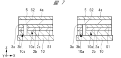
- 1 is a cross-sectional view of a semiconductor device during a manufacturing process according to a first embodiment
- 2 is a plan view showing an example of a layout of conductors used in manufacturing the semiconductor device according to the first embodiment
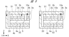
- 6 is a cross-sectional view of the semiconductor device during the manufacturing process subsequent to FIG. 5 .
- 8 is a cross-sectional view of the semiconductor device during the manufacturing process following FIG. 7 .
- FIG. 9 is a cross-sectional view of the semiconductor device during the manufacturing process following FIG. 8 .
- 10 is a cross-sectional view of the semiconductor device during the manufacturing process continued from FIG. 9 .
- 11 is a cross-sectional view of the semiconductor device during the manufacturing process subsequent to FIG. 10 .
- FIG. 1 is a plan view showing a semiconductor device according to a first modification of the first embodiment;
- FIG. 1 is a plan view showing a semiconductor device according to a first modification of the first embodiment;
- FIG. 1 is a plan view showing a semiconductor device according to a first modification of the first embodiment
- 11 is a cross-sectional view showing a semiconductor device according to a second modification of the first embodiment
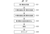
- 11 is a flow chart showing a manufacturing process of a semiconductor device according to a second modification of the first embodiment.
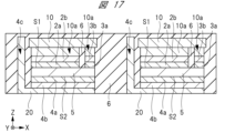
- 11A to 11C are cross-sectional views of a semiconductor device according to a second modification of the first embodiment during a manufacturing process.
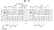
- 18 is a cross-sectional view of the semiconductor device during the manufacturing process following FIG. 17 .
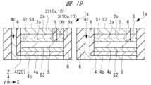
- 19 is a cross-sectional view of the semiconductor device during the manufacturing process following FIG. 18 .
- FIG. 11 is a plan view showing a semiconductor device according to a second embodiment.
- 21 is a cross-sectional view taken along line BB in FIG. 20.
- FIG. 21 is a cross-sectional view taken along line CC of FIG. 20.
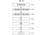
- 11 is a flow chart showing a manufacturing process of a semiconductor device according to a second embodiment.
- 11 is a cross-sectional view of a semiconductor device during a manufacturing process according to a second embodiment.
- 25 is a cross-sectional view of the semiconductor device during the manufacturing process following FIG. 24.
- 26 is a cross-sectional view of the semiconductor device during the manufacturing process following FIG. 25 .
- 27 is a cross-sectional view of the semiconductor device during the manufacturing process following FIG. 26.
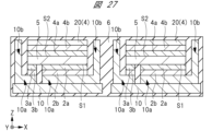
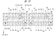
- 28 is a cross-sectional view of the semiconductor device during the manufacturing process following FIG. 27.
- FIG. 11 is a cross-sectional view showing a semiconductor device according to a modified example of the second embodiment.
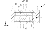
- FIG. 11 is a cross-sectional view showing a semiconductor device according to a modified example of the second embodiment.
- FIG. 11 is a cross-sectional view showing a semiconductor device according to a modified example of the second embodiment.
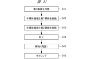
- 13 is a flow chart showing a manufacturing process of a semiconductor device according to a modification of the second embodiment.
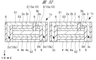
- 13 is a cross-sectional view of a semiconductor device according to a modification of the second embodiment during a manufacturing process.
- FIG. 11 is a cross-sectional view showing a semiconductor device according to a comparative example.
- FIG. 1 is a plan view showing a semiconductor module according to a comparative example.
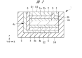
- the semiconductor chip 1 which is the semiconductor device of this embodiment, has terminals 2, 3, and 4 on the main surface S3 side.
- the semiconductor chip 1 has a main surface S3 and a main surface S4 opposite to the main surface S3.
- Both the main surface S3 and the main surface S4 are surfaces along the X direction and the Y direction.
- the X direction and the Y direction are directions perpendicular to each other.
- the thickness direction (height direction) of the semiconductor chip 1 is the Z direction perpendicular to each of the X direction and the Y direction.
- a planar view means viewing an object along the Z direction.
- the semiconductor chip 1 has a semiconductor substrate 5 therein.
- the semiconductor substrate 5 is made of, for example, Si (silicon), SiC (silicon carbide), GaN (gallium nitride), Ga 2 O 3 (gallium oxide), or diamond.
- the shape of the semiconductor substrate 5 in a plan view is rectangular.
- the semiconductor substrate 5 has a main surface S1 and a main surface S2 opposite to the main surface S1.
- the main surface S1 is a surface of the semiconductor substrate 5 located on the main surface S3 side
- the main surface S2 is a surface of the semiconductor substrate 5 located on the main surface S4 side.
- the main surface S3 is located on the bonding material (conductive connection layer) 2b side and the bonding material (conductive connection layer) 3b side with respect to the semiconductor substrate 5.
- the main surface S4 is located on the bonding material (conductive connection layer) 4b side with respect to the semiconductor substrate 5.
- the source electrode 2a and gate electrode 3a are connected to the main surface S1 of the semiconductor substrate 5.
- the drain electrode 4a is connected to the main surface S2 of the semiconductor substrate 5.
- the source electrode 2a, gate electrode 3a, and drain electrode 4a are spaced apart from each other and insulated from each other.
- the outermost surfaces (surfaces facing the main surface S3) of the source electrode 2a and gate electrode 3a are made of, for example, Ni (nickel) or Cu (copper).
- the outermost surface (surface facing the main surface S4) of the drain electrode 4a is made of, for example, Ni (nickel), Cu (copper), or Au (gold).
- the semiconductor substrate 5 is not composed of semiconductors alone, but has a layered structure including wiring and an insulating layer on its main surface, and is equipped with semiconductor elements.
- Possible semiconductor elements formed on the semiconductor substrate 5 include transistors such as MOSFETs (Metal Oxide Semiconductor Field Effect Transistors) and IGBTs (Insulated Gate Bipolar Transistors).
- the semiconductor elements formed on the semiconductor substrate 5 may also be rectifying elements such as diodes.
- the semiconductor substrate 5 is equipped with a MOSFET.
- the semiconductor substrate 5 is a three-terminal element. If the semiconductor element of the semiconductor substrate 5 is a two-terminal element such as a diode, there will be only one electrode and terminal connected to the surface on the main surface S3 side of the semiconductor substrate 5. There may be three or more electrodes and terminals connected to the surface on the main surface S3 side of the semiconductor substrate 5.
- a source sense terminal, a temperature detection terminal, etc. may be provided on the main surface S3 of the semiconductor substrate 5.
- the terminal 2 is connected to the surface of the source electrode 2a on the main surface S3 side via a bonding material 2b.
- the terminal 3 is connected to the surface of the gate electrode 3a on the main surface S3 side via a bonding material 3b.
- the terminal 4 is connected to the surface of the drain electrode 4a on the main surface S4 side via a bonding material 4b. That is, the terminal 2 is electrically connected to the semiconductor substrate 5 via the bonding material 2b and the source electrode 2a.
- the terminal 3 is electrically connected to the semiconductor substrate 5 via the bonding material 3b and the gate electrode 3a.
- the terminal 4 is electrically connected to the semiconductor substrate 5 via the bonding material 4b and the drain electrode 4a.
- Each of the terminals 2, 3, and 4 is made of, for example, Cu (copper), W (tungsten), Al (aluminum), or Mo (molybdenum).
- Each of the bonding materials (bonding layers) 2b, 3b, and 4b is a conductive joint, and is made of, for example, solder, sintered material, or bump.
- the terminal 4 extends outward in the Y and X directions relative to the stack consisting of the semiconductor substrate 5, source electrode 2a, gate electrode 3a, drain electrode 4a, bonding materials 2b, 3b, 4b, and terminals 2 and 3 stacked in the Z direction, and has an extraction electrode 4c that extends toward the main surface S3 at a position separated from the stack.
- the extraction electrode 4c which is part of the terminal 4, extends in the Z direction and is exposed on the main surface S3.
- the shape of the stack is rectangular in a plan view. As shown in FIG.
- the extraction electrode 4c (terminal 4) has an L-shaped planar layout in which a portion extending along one side of the stack extending in the Y direction and a portion extending along one side of the stack extending in the X direction are connected to each other.
- the terminal 4 has a plate-like portion that contacts the bonding material 4b and extends along the X-Y plane, an extraction electrode 4c that extends along the X-Z plane, and an extraction electrode 4c that extends along the Y-Z plane. For this reason, the terminal 4 has an L-shaped cross-sectional shape.
- the plate-like portion extending along the X-Y plane and the extraction electrode 4c may be integrated, or may be joined to each other via a bonding material.
- the manufacturing method of the terminal 4 (the conductor 20 described below) is simple, but since material processing is required, the manufacturing cost increases compared to when the plate-like portion and the extraction electrode 4c are joined.
- An insulating material (sealing material) 6 is embedded between the laminate and the extraction electrode 4c.
- An insulating material 6 is embedded between the laminate consisting of the source electrode 2a, bonding material 2b, and terminal 2 and the laminate consisting of the gate electrode 3a, bonding material 3b, and terminal 3.
- the insulating material 6 continuously covers and seals the side surfaces in the X and Y directions of the structure consisting of the terminal 4, semiconductor substrate 5, source electrode 2a, gate electrode 3a, drain electrode 4a, bonding materials 2b, 3b, 4b, and terminals 2, 3, and 4, as well as the surface on the main surface S4 side of the terminal 4.
- the insulating material 6 is made of, for example, a molded resin.
- the terminals 4 are extended from the position where they are bonded to the bonding material 4b toward the main surface S3 by a plate-like portion extending along the XY plane and an extraction electrode 4c.
- the terminals are not exposed on any surface of the semiconductor chip 1 other than the main surface S3. In other words, all surfaces of the semiconductor chip 1 other than the main surface S3 are covered with the insulating material 6.
- the shape of the semiconductor chip 1 in a plan view and the shape of each side are rectangular.
- the shape of the semiconductor chip 1 is a rectangular parallelepiped.
- the sides of the semiconductor chip 1 in the X and Y directions and the main surface S4 are made of insulating material 6, and the surface of the terminal 4 on the main surface S4 side is not exposed.
- the main surface S3 is made up of the insulating material 6 and the surfaces of the terminals 2, 3, and 4.
- the main surface S3 is flat.
- the periphery of each of the terminals 2, 3, and 4 is completely surrounded by the insulating material 6.
- terminal (gate terminal) 3 in a plan view is rectangular. In a plan view, the area of terminal (gate terminal) 3 is smaller than that of terminal (source terminal) 2. It is preferable that the shortest distance between each of 2, 3, and 4 is equal to or less than the length of one side (short side) of terminal 3 in a plan view. This is because if the shortest distance is large, the increase in size of the semiconductor device becomes a problem.
- Semiconductor substrate 5 is formed by cutting a semiconductor wafer into individual pieces.
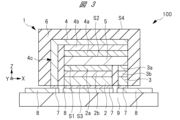
- FIG. 3 A cross-sectional view of a semiconductor module 100 on which a semiconductor device (semiconductor chip 1) according to the present embodiment is mounted is shown in Fig. 3.
- the semiconductor chip 1 shown in Fig. 3 is the semiconductor chip 1 shown in Fig. 2 turned upside down, and the position of the cross section shown in Fig. 3 is the same as the position of the cross section shown in Fig. 2.
- each of the terminals 2, 3, and 4 on the main surface S3 of the semiconductor chip 1 is connected to a separate wiring 8 via a bonding material 7.
- the wiring 8 is a wiring pattern made of a conductor provided on the main surface of an insulating substrate 9.
- the bonding material 7 is made of, for example, solder, a sintered material, or a bump.
- the insulating substrate 9 is made of, for example, AlN (aluminum nitride).
- the semiconductor module shown in FIG. 3 may be placed in, for example, a resin case, and the structure including the semiconductor chip 1 on the main surface of the insulating substrate 9 may be sealed with resin poured into the resin case.
- all terminals of the semiconductor chip 1 are surface-mounted on the insulating substrate 9 side using only bonding material 7 on the main surface S3 side.
- the semiconductor chip 1 and the wiring 8 are not connected using bonding wires or conductive ribbons, etc.
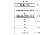
- a plurality of conductors 10 are prepared (step S11 in FIG. 4).
- the conductors 10 are made of, for example, Cu (copper), W (tungsten), Al (aluminum), or Mo (molybdenum).
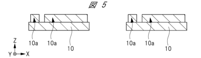
- the conductors 10 have a plate-shaped support portion and two convex portions 10a spaced apart from each other on the surface of the support portion. These two convex portions 10a are portions that will later become the terminals 2 and 3.
- a plurality of conductors 10 may be connected to each other via a connecting portion 10c and integrated.
- the conductors 10 shown in FIG. 5 have already been singulated.
- the singulated conductors 10 have the advantage of low material costs, but require a lot of work to align them with the semiconductor substrate to be connected in a later process.
- the integrated conductors 10 in FIG. 6 have the advantage of easy alignment, but high material costs.
- each of the multiple conductors 10 is connected to each of the multiple semiconductor substrates 5 (step S12 in FIG. 4).
- multiple semiconductor substrates 5 are prepared, each having a main surface S1 and a main surface S2 opposite to the main surface S1, with a source electrode 2a and a gate electrode 3a provided on the main surface S1, and a drain electrode 4a provided on the main surface S2.
- the source electrode 2a is connected to one of the two protruding portions 10a of each conductor 10 via a bonding material 2b
- the gate electrode 3a is connected to the other of the two protruding portions 10a via a bonding material 3b.
- a plurality of conductors 20 are connected to each of the plurality of semiconductor substrates 5 (step S13 in FIG. 4). That is, a plurality of conductors 20 are prepared, each of which is configured by connecting a plate-like portion extending along the X-Y plane, an extraction electrode (convex portion) 4c extending along the X-Z plane, and an extraction electrode (convex portion) 4c extending along the Y-Z plane.
- the extraction electrode 4c is connected to the surface of the plate-like portion, which is the support portion, and is formed on the surface.
- the plurality of semiconductor substrates 5 may be prepared at the time of step S11, and the plurality of conductors 20 may be prepared at the time of step S11 or S12.
- Steps S12 and S13 may be performed simultaneously. That is, the conductors 10 and 20 may be connected to the semiconductor substrate 5 at the same time. Also, step S13 may be performed before step S12.
- the conductor 10 and the semiconductor substrate 5, which are connected to each other, are turned upside down.
- the drain electrode 4a on the main surface S4 side of the semiconductor substrate 5 is connected via a bonding material 4b to the surface of the plate-like portion of each conductor 20 that extends along the X-Y plane and is the surface from which the extraction electrode 4c protrudes.
- the stack consisting of the semiconductor substrate 5, source electrode 2a, gate electrode 3a, drain electrode 4a, bonding materials 2b, 3b, 4b, and terminals 2 and 3 is connected to the surface of the plate-like portion with the extraction electrode 4c spaced apart in the Y and X directions.
- Each of the bonding materials 2b, 3b, and 4b is, for example, solder, sintered material, or bump.
- the semiconductor substrates 5 and the conductors 10 and 20 are each sealed with an insulating material 6 (step S14 in FIG. 4).
- the insulating material 6 is made of, for example, a molded resin.
- the entire surfaces of the conductors 10 and 20 are sealed, but a part of the surfaces of the conductors 10 and 20 (the upper ends of the conductors in FIG. 9) may be exposed above the bonding materials 2b and 3b.
- the height positions of the upper surface of the conductor 10 (the surface opposite the semiconductor substrate 5) and the top surface of the conductor 20 may not coincide with each other. This is because these upper surfaces will be flattened by grinding in a later step S15.
- the surfaces of the insulating material 6, conductor 10, and conductor 20 are flattened by grinding the conductors 10 and 20 from above (step S15 in FIG. 4).
- the support portion constituting the conductor 10 is removed, and grinding is continued until the two protruding portions 10a are separated from each other.
- the two protruding portions 10a of the conductor 10 that remain thereby constitute terminals 2 and 3, respectively.
- the conductor 20, which has been partially ground, constitutes terminal 4.
- the surfaces of the insulating material 6 and terminals 2, 3, and 4 that have been flattened in this grinding process constitute the main surface S3.
- step S16 in FIG. 4 dicing is performed to cut away the insulating material 6 between adjacent terminals 4, thereby obtaining a plurality of individual semiconductor chips 1 (step S16 in FIG. 4).
- the semiconductor chip 1 and an insulating substrate 9 having a pattern of wiring 8 on its main surface are prepared, and then each of the terminals 2, 3, and 4 exposed on the main surface S3 of the semiconductor chip 1 is connected to each of the wiring 8 via a bonding material 7.
- a continuity test is performed on a semiconductor chip.
- the test is performed by applying a voltage to each terminal of the semiconductor chip, so that it is necessary to prevent air discharge between the terminals during the test for off-characteristic evaluation.
- a voltage for example, in the test of an element such as a SiC power semiconductor element, to which a higher voltage is applied than a Si semiconductor element, a high electric field is applied, so that it is necessary to take measures to prevent discharge.
- possible test methods include immersing the semiconductor device in an insulating liquid or performing measurements under pressure, but it is difficult to perform measurements in the chip state.
- testing can be performed after multiple semiconductor chips are connected in parallel (see Figure 34), sealed with insulating material, and modularized with a bus bar for connecting the main current path.
- Figure 34 sealed with insulating material, and modularized with a bus bar for connecting the main current path.
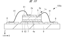
- bonding wires 41 When semiconductor chips are connected in parallel to form a semiconductor module, it is possible to use bonding wires 41, as shown as comparative examples in Figures 33 and 34.
- the insulating material (sealing material) is omitted
- Figure 34 the insulating material and some of the bonding wires 41 are omitted.
- the semiconductor chip 1x which is a semiconductor device of the comparative example, differs from the semiconductor chip 1 shown in FIG. 1 in that it is electrically connected to the drain electrode 4a of the semiconductor substrate 5 and does not have an electrode (terminal) that draws the drain to the source electrode 2a and gate electrode 3a. In addition, it does not have electrodes that are electrically connected to each of the source electrode 2a and gate electrode 3a of the semiconductor substrate 5 and draw the source and gate to the drain electrode 4a.
- the drain electrode 4a is connected to the wiring 8 via a bonding material 7 directly below the semiconductor substrate 5, and the source electrode 2a and the gate electrode 3a are each connected to the wiring 8 via a bonding wire 41 that contacts their upper surfaces.
- the semiconductor module 100a of this comparative example in addition to the surface mounting process for connecting the drain electrode 4a to the wiring 8, a wire bonding process is required, which increases the manufacturing cost of the semiconductor device. Also, if the bonding wire 41 is formed at a high position as shown in FIG. 33, the resin layer for sealing the semiconductor chip 1x and the bonding wire 41 must be thickened, which causes a problem of an increase in the size of the semiconductor device.
- an extraction electrode 4c is provided at a position spaced apart from the semiconductor substrate 5, which extracts the terminal 4 on the main surface S4 side of the semiconductor chip 1 to the main surface S3 side.
- the semiconductor chip 1 As a result, in the inspection process of the semiconductor device, it is possible to inspect the semiconductor chip 1 as a single chip without connecting multiple semiconductor chips in parallel. This is because the semiconductor chip 1 is sealed with the insulating material 6, and also because inspection is easy with the main surface S4 glued or adsorbed. Since there are no terminals on the main surface S4, it is also easy to inspect the semiconductor chip 1 by immersing it in an insulating liquid or applying pressure by fixing the main surface S4. This prevents discharge and enables inspection of the semiconductor chip 1 as a single chip at high voltage. This eliminates the need to connect multiple semiconductor chips in parallel for inspection, and prevents other semiconductor chips from being treated as defective due to a defect in one semiconductor chip. This improves the yield of semiconductor devices and prevents an increase in the manufacturing cost of semiconductor devices.
- the semiconductor device can be mounted only through the surface mounting process using the bonding material 7, which reduces the manufacturing costs of the semiconductor device.
- the size of the semiconductor device can be reduced.
- the resin layer for sealing the semiconductor chip 1 can be made thinner than in the comparative example, which allows the size of the semiconductor device to be reduced.
- the planar layout of the terminals 4 (lead electrodes 4c) on the main surface S3 of the semiconductor chip 1 is not limited to an L-shape, and may be a shape as shown in Figures 12 and 13.
- the terminals 4 have an I-shape extending only along one side of the terminals 2, which have a substantially rectangular planar shape.
- the terminals 4 have a U-shape extending continuously along three sides of the terminals 2.
- the terminals 4 have a continuous rectangular ring-shaped structure extending along the four sides of the terminals 2.
- the surface of the terminal 4 may be exposed from the insulating material 6.
- a plate-like portion that contacts the bonding material 4b and extends along the XY plane is partially exposed.
- the surface opposite the semiconductor substrate 5 is exposed from the insulating material 6.
- steps S11 to S13 in FIG. 4 are carried out (steps S21 to S23 in FIG. 16).
- the multiple semiconductor substrates 5 and the multiple conductors 10 and 20 are each sealed with an insulating material 6 (step S24 in FIG. 16).
- sealing is performed with the surface (bottom surface) of each of the multiple conductors 20 opposite the semiconductor substrate 5 side adhered to a tape (not shown) to cover (protect) it.
- the conductor 20 may be sealed as in step S14 of FIG. 4, and then grinded to expose the surface of the conductor 20 opposite the semiconductor substrate 5 (the bottom surface), thereby obtaining the structure shown in FIG. 17.
- step S15 in FIG. 4 is performed to form terminals 2, 3, and 4 (step S25 in FIG. 16).
- step S26 in FIG. 16 a dicing process similar to step S16 in FIG. 4 is performed to obtain a plurality of individual semiconductor chips 1a (step S26 in FIG. 16). With the above steps, the semiconductor device of this modified example is substantially completed.
- the same effects as those of the semiconductor device described with reference to Figures 1 to 3 can be obtained.
- the absence of insulating material 6 covering the terminals 4 on the main surface S4 allows the size of the semiconductor device to be reduced, and the cooling effect on the main surface S4 side to be increased. It also becomes possible to perform inspection and measurement by contacting a probe with both the main surface S3 side and the main surface S4 side.
- the exposed area of the terminals 4 on the main surface S4 side is larger than the exposed area of the terminals 4 on the main surface S3 side. This makes probe inspection of the terminals 4 easier.
- FIG. 20 shows the main surface S4 of the semiconductor chip 1b, unlike FIG. 1.
- the main surface S4 of the semiconductor chip 1b exposes the terminal 4 connected to the drain electrode 4a of the semiconductor substrate 5 via the bonding material 4b.
- the main surface S4 also exposes the terminal 2 (extraction electrode 2c) connected to the source electrode 2a of the semiconductor substrate 5 via the bonding material 2b.
- the main surface S4 also exposes the terminal 3 (extraction electrode 3c) connected to the gate electrode 3a of the semiconductor substrate 5 via the bonding material 3b.
- the terminal 2 on the main surface S4 has an L-shaped layout.
- the shapes of the terminals 2 and 3 on the main surface S4 may be any of the L-shaped, I-shaped, and U-shaped shapes described with reference to FIGS. 1, 12, and 13.
- terminal 3 has a plate-shaped portion that contacts bonding material 3b and extends along the X-Y plane, and extraction electrode 3c that extends along the X-Z plane.
- terminal 2 has a plate-shaped portion that contacts bonding material 2b and extends along the X-Y plane, extraction electrode 2c that extends along the X-Z plane, and extraction electrode 2c that extends along the Y-Z plane.
- Each of extraction electrodes 2c, 3c extends in the Z direction, and one end of the extension direction terminates at main surface S4. Terminals 2 and 3, which are aligned in the X and Y directions, are spaced apart from each other.
- the terminals are not exposed.
- the entire surface is covered with the insulating material 6.
- a plurality of conductors 10 are prepared (step S31 in FIG. 23).
- the conductor 10 has a support portion, and has two convex portions 10a spaced apart from each other on the surface of the support portion.
- the two convex portions 10a are portions that will later become the terminals 2 and 3.
- Each of the two convex portions 10a further has a convex portion 10b that protrudes from its upper surface.
- the convex portion 10a is formed on the surface of the support portion via the convex portion 10b.
- the two convex portions 10b are portions that will later become the lead electrodes 2c and 3c, which are parts of the terminals 2 and 3, respectively.
- the conductor 10 is composed of the support portion and the convex portions 10a and 10b.
- each of the conductors 10 is connected to each of the semiconductor substrates 5 (step S32 in FIG. 23).
- a plurality of semiconductor substrates 5 are prepared, each of which has a main surface S1 and a main surface S2 opposite to the main surface S1, with a source electrode 2a and a gate electrode 3a provided on the main surface S1 and a drain electrode 4a provided on the main surface S2.
- the source electrode 2a is connected to one of the two protruding portions 10a of each conductor 10 via a bonding material 2b
- the gate electrode 3a is connected to the other of the two protruding portions 10a via a bonding material 3b.
- the semiconductor substrate 5 is connected to the protruding portion 10a at a position separated from the protruding portion 10b.
- the stack including the semiconductor substrate 5 and the drain electrode 4a is separated from the protruding portion 10b, and the source electrode 2a and the gate electrode 3a are connected to the surface of the plurality of protruding portions 10a, which is the surface of the conductor 10, via the bonding materials 2b and 3b.
- a number of conductors 20 are connected to each of a number of semiconductor substrates 5 (step S33 in FIG. 23).
- the conductors 20 are made up of only plate-like portions extending along the X-Y plane, and form terminals 4.
- the drain electrode 4a on the main surface S2 side of the semiconductor substrate 5 is connected to the surface of each conductor 20 via a bonding material 4b.
- the conductors 20 are connected to the semiconductor substrate 5 at a position spaced apart from the protrusion 10b.
- Steps S32 and S33 may be performed simultaneously. That is, the conductors 10 and 20 may be connected to the semiconductor substrate 5 at the same time. Also, step S33 may be performed before step S32.
- the multiple semiconductor substrates 5 and the multiple conductors 10 and 20 are each sealed with an insulating material 6 (step S34 in FIG. 23).
- steps S34 in FIG. 23 parts of the surfaces of the conductors 10 and 20 are exposed, but the entire surfaces of the conductors 10 and 20 may be sealed.
- the height positions of the top surface of the conductor 20 (the surface opposite the semiconductor substrate 5) and the top surface of the conductor 10 (protrusion 10b) in the Z direction may not coincide but may be offset. This is because these top surfaces will be flattened by grinding performed later in step S35.
- conductor 10 and conductor 20 are ground from both sides in the Z direction (step S35 in FIG. 23).
- the structure including the semiconductor substrate 5, conductors 10, 20, and insulating material 6 is turned upside down.
- the conductor 10 is ground from above. That is, the conductor 10 and insulating material 6 are ground until the support portion constituting the conductor 10 is removed and the two protruding portions 10a are separated from each other. As a result, the remaining pair of protruding portions 10a, 10b constitutes the terminal 2, and the other pair of protruding portions 10a, 10b constitutes the terminal 3.
- step S36 the sealing process is carried out again (step S36 in FIG. 23).
- the terminals 2 and 3 (protruding portions 10a) exposed by the grinding are covered with insulating material 6.
- this insulating material 6 and the insulating material 6 formed in step S34 are formed in separate processes, they are given the same reference numerals here and are shown integrated together in FIG. 28.
- the semiconductor chip 1b the flat surface including the insulating material 6 exposed on the lower side of FIG. 28 (the bonding material 4b side relative to the semiconductor substrate 5) and the respective surfaces of the terminals 2, 3, and 4 constitutes the main surface S4.
- the semiconductor device and manufacturing method thereof of this embodiment provide the same effects as those of the first embodiment. Furthermore, the semiconductor chip 1b of this embodiment has higher heat dissipation properties than the semiconductor chip 1 of the first embodiment. This is because the surface area of the semiconductor chip 1b in plan view that is occupied by conductors (terminals) is larger on the surface on which the drain electrode 4a is formed than on the surface on which the source electrode 2a and gate electrode 3a are formed. In other words, in this embodiment, heat can be dissipated from almost the entire main surface S4, so the thermal resistance is low.
- the surfaces of the terminals 2 and 3 may be exposed from the insulating material 6.
- the surfaces opposite to the main surface S1 of the semiconductor substrate 5 are exposed from the insulating material 6.
- the cross sections shown in FIGS. 29 and 30 are at locations corresponding to the cross sections shown in FIGS. 21 and 22.
- steps S31 to S34 in FIG. 23 are carried out (steps S41 to S44 in FIG. 31).
- both surfaces of the conductor 10 and the conductor 20 in the Z direction are ground to flatten both surfaces of the insulating material 6, the conductor 10, and the conductor 20 (step S45 in FIG. 31), and then dicing is performed (step S46 in FIG. 31).
- a sealing process is not performed again. As a result, the surfaces of the terminals 2 and 3 remain exposed from the insulating material 6.
- the semiconductor chip 1c the flat surface including the surfaces of the insulating material 6 and the terminals 2, 3, and 4 exposed on the bonding material 4b side relative to the semiconductor substrate 5 constitutes the main surface S4.
- the flat surface on the opposite side of the main surface S4 of the semiconductor chip 1c (the surface on the bonding material 2b side relative to the semiconductor substrate 5) including the surfaces of the insulating material 6 and the terminals 2 and 3 constitutes the main surface S3.
- the present invention can be widely used in semiconductor devices and their manufacturing methods.
Landscapes
- Structures Or Materials For Encapsulating Or Coating Semiconductor Devices Or Solid State Devices (AREA)
Abstract
Description
以下に、図1~図3を用いて、本実施の形態の半導体装置の構造について説明する。本実施の形態の半導体装置である半導体チップ1は、図1に示すように、主面S3側に端子2、端子3および端子4を備えるものである。半導体チップ1は、図2に示すように、主面S3と、主面S3と反対側の主面S4とを備えている。主面S3および主面S4は、いずれもX方向およびY方向に沿う面である。X方向およびY方向は、互いに直交する方向である。半導体チップ1の厚さ方向(高さ方向)は、X方向およびY方向のそれぞれに対し直交するZ方向である。本願でいう平面視とは、Z方向に沿って対象物を見ることを意味する。
本実施の形態の半導体装置(半導体チップ1)を搭載(実装)した半導体モジュール100の断面図を図3に示す。図3に示す半導体チップ1は、図2に示す半導体チップ1の上下を逆さにしたものであり、図3に示す断面の位置は図2に示す断面の位置と同じである。
次に、図4のフローを参照しつつ、図5~図11を用いて、本実施の形態の半導体装置の製造方法について説明する。
半導体装置の製造工程においては、半導体チップに対して導通検査が行われる。検査では、半導体チップの各端子に対し電圧を印加することで行われるため、オフ特性評価のための検査の際には端子間での気中放電を防止する必要がある。例えばSiCパワー半導体素子のように、Si半導体素子に比べ高い電圧が印加される素子の検査では高電界が印加されるため、特に放電防止のための対策を講じる必要がある。放電防止のため、検査方法としては半導体装置を絶縁の液体に浸す、または加圧した状態で測定を行う手段が考えられるが、チップ状態での測定は難しい。
半導体チップ1の主面S3における端子4(引き出し電極4c)の平面レイアウトは、L字型に限らず図12~図13に示すような形状であってもよい。図12に示す平面レイアウトにおいて、端子4は、平面形状が略矩形である端子2の1辺にのみ沿って延在するI字型の形状を有している。図13に示す平面レイアウトにおいて、端子4は、端子2の3辺に沿って連続的に延在するU字型の形状を有している。図14に示す平面レイアウトにおいて、端子4は、端子2の4辺に沿う連続的な矩形の環状構造を有している。
図15に示すように、半導体チップ1aの主面S4において、端子4の表面が絶縁材6から露出していてもよい。ここでは、端子4を構成する部分のうち、接合材4bに接してX-Y平面に沿って延在する板状部分の一部が露出している。つまり、当該板状部分の面のうち、半導体基板5と反対側の面が、絶縁材6から露出している。
上記実施の形態1では、ドレイン電極4aに接続された端子4を他の端子2、3の形成された方に引き出すことについて説明したが、以下では、逆に端子2、3を端子4の形成された主面S4側に引き出すことについて、図20~図28を用いて説明する。
図29および図30に示すように、半導体チップ1cの主面S3において、端子2、3の表面が絶縁材6から露出していてもよい。ここでは、端子2、3の面のうち、半導体基板5の主面S1と反対側の面が、絶縁材6から露出している。図29および図30に示す断面、図21および図22に示す断面に対応する箇所における断面である。
2、3、4 端子
2a ソース電極
2b、3b、4b、7 接合材
2c、3c、4c 引き出し電極
3a ゲート電極
4a ドレイン電極
5 半導体基板
6 絶縁材
8 配線
9 絶縁基板
10、20 導体
10a、10b 凸部
10c 接続部
41 ボンディングワイヤ
100、100a 半導体モジュール
S1、S2、S3、S4 主面
Claims (14)
- 第1主面と、前記第1主面の反対側の第2主面と、半導体素子とを備えた半導体基板と、
前記第1主面に接して設けられた第1電極に、導電性を有する第1接合材を介して接続された第1端子と、
前記第2主面に接して設けられた第2電極に、導電性を有する第2接合材を介して接続され、前記第1端子とは絶縁された第2端子と、
前記第1端子および前記第2端子のそれぞれの一部と前記半導体基板とを封止する絶縁材と、
前記半導体基板に対し前記第1接合材側に位置し、前記第1端子および前記第2端子が露出する第3主面と、
前記第3主面の反対側の第4主面と、
を有し、
前記第2端子は、前記半導体基板、前記第1電極および前記第1接合材を含む積層体から離間する引き出し電極により、前記第3主面側に引き出され、
前記第1端子および前記第2端子の相互間は、前記絶縁材により絶縁されている、半導体装置。 - 請求項1記載の半導体装置において、
前記第3主面以外の表面において端子が露出していない、半導体装置。 - 請求項1記載の半導体装置において、
前記第4主面では、前記第2端子が露出している、半導体装置。 - 請求項1記載の半導体装置において、
前記第1端子が複数形成され、
前記第1主面に接して形成された複数の前記第1電極それぞれに対し、前記第1接合材を介して複数の前記第1端子のそれぞれが接続され、
前記第3主面には、複数の前記第1端子が露出している、半導体装置。 - 請求項1記載の半導体装置において、
前記第2端子が複数形成され、
前記第2主面に接して形成された複数の前記第2電極それぞれに対し、前記第2接合材を介して複数の前記第2端子のそれぞれが接続され、
前記第3主面には、複数の前記第2端子が露出している、半導体装置。 - 請求項5記載の半導体装置において、
前記第4主面には、複数の前記第2端子が露出している、半導体装置。 - 請求項5記載の半導体装置において、
前記第3主面で露出する前記第1端子の平面視における形状は、略矩形であり、
前記第3主面で露出する前記第2端子は、平面視において、前記第1端子の1つの辺、2つの辺、3つの辺または4つの辺に沿って延在している、半導体装置。 - 以下の工程を含む、半導体装置の製造方法:
(a)第1主面と、前記第1主面の反対側の第2主面と、半導体素子とを備え、前記第1主面に第1電極が接し、前記第2主面に第2電極が接する半導体基板を用意する工程;
(b)前記第1電極に、導電性を有する第1接合材を介して第1導体を接続する工程;
(c)表面に第1凸部を有する第2導体を用意する工程;
(d)前記半導体基板および前記第1電極を含む積層体と、前記第1凸部とを離間させて、前記第2導体の前記表面に、導電性を有する第2接合材を介して前記第2電極を接続する工程;
(e)前記(a)~(d)工程の後、前記半導体基板、前記第1導体および前記第2導体を絶縁材により封止する工程;
ここで、前記半導体装置は、前記第1導体からなる第1端子、および、前記第2導体からなる第2端子のそれぞれが露出する第3主面と、前記第3主面の反対側の第4主面とを有し、
前記第3主面は、前記半導体基板に対し前記第1接合材側に位置し、
前記第1端子と前記第2端子とは、互いに絶縁され、
前記第2端子は、前記第1凸部により、前記第3主面側に引き出されている。 - 請求項8記載の半導体装置の製造方法において、
(f)前記(e)工程の後、研削により前記絶縁材の一部を除去することで、前記第3主面において前記第1導体および前記第2導体を前記絶縁材から露出させる工程;
をさらに有する、半導体装置の製造方法。 - 請求項9記載の半導体装置の製造方法において、
(b1)前記(b)工程の前に、第1支持部と、前記第1支持部の表面上に並ぶ複数の第2凸部とを有する前記第1導体を用意する工程;
をさらに有し、
前記(a)工程では、互いに絶縁された複数の第1電極が前記第1主面に接する前記半導体基板を用意し、
前記(b)工程では、複数の前記第1電極のそれぞれに、前記第1接合材を介して複数の前記第2凸部のそれぞれを接続し、
前記(f)工程では、研削により前記絶縁材の一部および前記第1支持部を除去することで、前記第3主面において、互いに離間する複数の前記第2凸部と、前記第2導体とを前記絶縁材から露出させ、
前記第3主面において露出する複数の前記第2凸部は、互いに絶縁された複数の前記第1端子を構成している、半導体装置の製造方法。 - 請求項8記載の半導体装置の製造方法において、
前記(e)工程では、前記第4主面を構成する前記第2導体の面を除き、前記半導体基板、前記第1導体および前記第2導体を前記絶縁材により封止する、半導体装置の製造方法。 - 請求項9記載の半導体装置の製造方法において、
(f1)前記(e)工程の後、研削により前記絶縁材の一部を除去することで、前記第4主面において前記第2導体を前記絶縁材から露出させる工程;
をさらに有する、半導体装置の製造方法。 - 請求項8記載の半導体装置の製造方法において、
(f2)前記(e)工程の後、研削により前記絶縁材の一部および前記第2導体の一部を除去する工程;
をさらに有し、
前記(a)工程では、互いに絶縁された複数の第2電極が前記第2主面に接する前記半導体基板を用意し、
前記(c)工程では、第2支持部と、前記第2支持部の表面上に形成された複数の第3凸部と、前記第2支持部の前記表面上に複数の前記第3凸部のそれぞれを介して形成された複数の前記第1凸部と、を備えた前記第2導体を用意し、
前記(d)工程では、複数の前記第2電極を含む前記積層体と、複数の前記第1凸部とを離間させて、前記第2導体の前記表面である複数の前記第3凸部の表面に、前記第2接合材を介して複数の前記第2電極のそれぞれを接続し、
前記(f2)工程では、研削により前記絶縁材の前記一部と前記第2導体の前記一部である前記第2支持部とを除去することで、前記第4主面において、互いに離間する複数の前記第3凸部を前記絶縁材から露出させ、
前記第4主面において露出する複数の前記第3凸部は、互いに絶縁された複数の前記第2端子を構成している、半導体装置の製造方法。 - 請求項13記載の半導体装置の製造方法において、
(f3)前記(f2)工程の後、前記第4主面において複数の前記第2端子を封止する工程;
をさらに有する、半導体装置の製造方法。
Priority Applications (1)
| Application Number | Priority Date | Filing Date | Title |
|---|---|---|---|
| CN202380090863.XA CN120530493A (zh) | 2023-02-21 | 2023-11-30 | 半导体器件及其制造方法 |
Applications Claiming Priority (2)
| Application Number | Priority Date | Filing Date | Title |
|---|---|---|---|
| JP2023025416A JP2024118861A (ja) | 2023-02-21 | 2023-02-21 | 半導体装置およびその製造方法 |
| JP2023-025416 | 2023-02-21 |
Publications (1)
| Publication Number | Publication Date |
|---|---|
| WO2024176559A1 true WO2024176559A1 (ja) | 2024-08-29 |
Family
ID=92500694
Family Applications (1)
| Application Number | Title | Priority Date | Filing Date |
|---|---|---|---|
| PCT/JP2023/042897 Ceased WO2024176559A1 (ja) | 2023-02-21 | 2023-11-30 | 半導体装置およびその製造方法 |
Country Status (3)
| Country | Link |
|---|---|
| JP (1) | JP2024118861A (ja) |
| CN (1) | CN120530493A (ja) |
| WO (1) | WO2024176559A1 (ja) |
Citations (7)
| Publication number | Priority date | Publication date | Assignee | Title |
|---|---|---|---|---|
| JP2006066813A (ja) * | 2004-08-30 | 2006-03-09 | Renesas Technology Corp | 半導体装置 |
| WO2006068641A1 (en) * | 2004-12-20 | 2006-06-29 | Semiconductor Components Industries, L.L.C. | Electronic package having down-set leads and method |
| JP2009188376A (ja) * | 2008-01-09 | 2009-08-20 | Toyota Motor Corp | 半導体装置とその製造方法 |
| WO2018198990A1 (ja) * | 2017-04-24 | 2018-11-01 | ローム株式会社 | 電子部品および半導体装置 |
| JP2022048197A (ja) * | 2016-12-28 | 2022-03-25 | ローム株式会社 | 半導体装置 |
| WO2022122527A1 (en) * | 2020-12-08 | 2022-06-16 | Hitachi Energy Switzerland Ag | Semiconductor module and manufacturing method |
| EP4020547A2 (en) * | 2020-12-23 | 2022-06-29 | STMicroelectronics S.r.l. | Packaged electronic device with high thermal dissipation and manufacturing process thereof |
-
2023
- 2023-02-21 JP JP2023025416A patent/JP2024118861A/ja active Pending
- 2023-11-30 CN CN202380090863.XA patent/CN120530493A/zh active Pending
- 2023-11-30 WO PCT/JP2023/042897 patent/WO2024176559A1/ja not_active Ceased
Patent Citations (7)
| Publication number | Priority date | Publication date | Assignee | Title |
|---|---|---|---|---|
| JP2006066813A (ja) * | 2004-08-30 | 2006-03-09 | Renesas Technology Corp | 半導体装置 |
| WO2006068641A1 (en) * | 2004-12-20 | 2006-06-29 | Semiconductor Components Industries, L.L.C. | Electronic package having down-set leads and method |
| JP2009188376A (ja) * | 2008-01-09 | 2009-08-20 | Toyota Motor Corp | 半導体装置とその製造方法 |
| JP2022048197A (ja) * | 2016-12-28 | 2022-03-25 | ローム株式会社 | 半導体装置 |
| WO2018198990A1 (ja) * | 2017-04-24 | 2018-11-01 | ローム株式会社 | 電子部品および半導体装置 |
| WO2022122527A1 (en) * | 2020-12-08 | 2022-06-16 | Hitachi Energy Switzerland Ag | Semiconductor module and manufacturing method |
| EP4020547A2 (en) * | 2020-12-23 | 2022-06-29 | STMicroelectronics S.r.l. | Packaged electronic device with high thermal dissipation and manufacturing process thereof |
Also Published As
| Publication number | Publication date |
|---|---|
| CN120530493A (zh) | 2025-08-22 |
| JP2024118861A (ja) | 2024-09-02 |
Similar Documents
| Publication | Publication Date | Title |
|---|---|---|
| US11257733B2 (en) | Semiconductor device including heat-dissipating metal multilayer having different thermal conductivity, and method for manufacturing same | |
| TWI730028B (zh) | 半導體裝置及其製造方法 | |
| US10727209B2 (en) | Semiconductor device and semiconductor element with improved yield | |
| JP5420274B2 (ja) | 半導体装置及びその製造方法 | |
| US8575744B2 (en) | Semiconductor device and lead frame thereof | |
| US7842545B2 (en) | Semiconductor package having insulated metal substrate and method of fabricating the same | |
| US11211373B1 (en) | Double-sided chip stack assembly | |
| US20080136015A1 (en) | High power semiconductor device | |
| US11387172B2 (en) | Semiconductor device and method for manufacturing the same | |
| CN111816633B (zh) | 半导体装置及半导体装置的制造方法 | |
| JP2024505028A (ja) | 熱伝導性接着層を備えた基板を有するパッケージ化された電子デバイス | |
| CN110634812A (zh) | 具有夹互连和双侧冷却的半导体器件封装 | |
| CN112768427A (zh) | 氮化镓hemt的封装结构及封装方法 | |
| CN110890419B (zh) | 半导体装置的制造方法 | |
| US20130256920A1 (en) | Semiconductor device | |
| JP2023041490A (ja) | 半導体装置 | |
| WO2024176559A1 (ja) | 半導体装置およびその製造方法 | |
| US11450623B2 (en) | Semiconductor device | |
| CN114792671A (zh) | 半导体装置、功率模块及半导体装置的制造方法 | |
| US20240282699A1 (en) | Semiconductor device | |
| CN223566612U (zh) | 一种GaN芯片的封装结构和电子设备 | |
| US20250374648A1 (en) | Semiconductor device, power conversion apparatus, and method for manufacturing the same | |
| US20230078259A1 (en) | Semiconductor device | |
| WO2022196123A1 (ja) | 半導体装置 | |
| WO2023095681A1 (ja) | 半導体装置 |
Legal Events
| Date | Code | Title | Description |
|---|---|---|---|
| 121 | Ep: the epo has been informed by wipo that ep was designated in this application |
Ref document number: 23924203 Country of ref document: EP Kind code of ref document: A1 |
|
| WWE | Wipo information: entry into national phase |
Ref document number: 202380090863.X Country of ref document: CN |
|
| WWP | Wipo information: published in national office |
Ref document number: 202380090863.X Country of ref document: CN |
|
| NENP | Non-entry into the national phase |
Ref country code: DE |
|
| 122 | Ep: pct application non-entry in european phase |
Ref document number: 23924203 Country of ref document: EP Kind code of ref document: A1 |