WO2024176381A1 - 電位生成回路、逆流防止回路、及び電位生成回路の制御方法 - Google Patents
電位生成回路、逆流防止回路、及び電位生成回路の制御方法 Download PDFInfo
- Publication number
- WO2024176381A1 WO2024176381A1 PCT/JP2023/006451 JP2023006451W WO2024176381A1 WO 2024176381 A1 WO2024176381 A1 WO 2024176381A1 JP 2023006451 W JP2023006451 W JP 2023006451W WO 2024176381 A1 WO2024176381 A1 WO 2024176381A1
- Authority
- WO
- WIPO (PCT)
- Prior art keywords
- potential
- circuit
- output
- terminal
- signal
- Prior art date
- Legal status (The legal status is an assumption and is not a legal conclusion. Google has not performed a legal analysis and makes no representation as to the accuracy of the status listed.)
- Ceased
Links
Images


Classifications
-
- H—ELECTRICITY
- H02—GENERATION; CONVERSION OR DISTRIBUTION OF ELECTRIC POWER
- H02H—EMERGENCY PROTECTIVE CIRCUIT ARRANGEMENTS
- H02H3/00—Emergency protective circuit arrangements for automatic disconnection directly responsive to an undesired change from normal electric working condition with or without subsequent reconnection ; integrated protection
- H02H3/003—Emergency protective circuit arrangements for automatic disconnection directly responsive to an undesired change from normal electric working condition with or without subsequent reconnection ; integrated protection responsive to reversal of power transmission direction
-
- H—ELECTRICITY
- H02—GENERATION; CONVERSION OR DISTRIBUTION OF ELECTRIC POWER
- H02M—APPARATUS FOR CONVERSION BETWEEN AC AND AC, BETWEEN AC AND DC, OR BETWEEN DC AND DC, AND FOR USE WITH MAINS OR SIMILAR POWER SUPPLY SYSTEMS; CONVERSION OF DC OR AC INPUT POWER INTO SURGE OUTPUT POWER; CONTROL OR REGULATION THEREOF
- H02M3/00—Conversion of DC power input into DC power output
- H02M3/02—Conversion of DC power input into DC power output without intermediate conversion into AC
- H02M3/04—Conversion of DC power input into DC power output without intermediate conversion into AC by static converters
- H02M3/10—Conversion of DC power input into DC power output without intermediate conversion into AC by static converters using discharge tubes with control electrode or semiconductor devices with control electrode
- H02M3/145—Conversion of DC power input into DC power output without intermediate conversion into AC by static converters using discharge tubes with control electrode or semiconductor devices with control electrode using devices of a triode or transistor type requiring continuous application of a control signal
- H02M3/155—Conversion of DC power input into DC power output without intermediate conversion into AC by static converters using discharge tubes with control electrode or semiconductor devices with control electrode using devices of a triode or transistor type requiring continuous application of a control signal using semiconductor devices only
- H02M3/156—Conversion of DC power input into DC power output without intermediate conversion into AC by static converters using discharge tubes with control electrode or semiconductor devices with control electrode using devices of a triode or transistor type requiring continuous application of a control signal using semiconductor devices only with automatic control of output voltage or current, e.g. switching regulators
- H02M3/158—Conversion of DC power input into DC power output without intermediate conversion into AC by static converters using discharge tubes with control electrode or semiconductor devices with control electrode using devices of a triode or transistor type requiring continuous application of a control signal using semiconductor devices only with automatic control of output voltage or current, e.g. switching regulators including plural semiconductor devices as final control devices for a single load
-
- H—ELECTRICITY
- H02—GENERATION; CONVERSION OR DISTRIBUTION OF ELECTRIC POWER
- H02J—ELECTRIC POWER NETWORKS; CIRCUIT ARRANGEMENTS OR SYSTEMS FOR SUPPLYING OR DISTRIBUTING ELECTRIC POWER; SYSTEMS FOR STORING ELECTRIC ENERGY
- H02J1/00—Circuit arrangements for DC mains or DC distribution networks
Definitions
- the present invention relates to a potential generating circuit, a backflow prevention circuit, and a method for controlling a potential generating circuit.
- a potential generating circuit capable of generating multiple output potentials has been known for some time.
- U.S. Patent No. 7,432,614 discloses an electric circuit that includes a plurality of output nodes, a plurality of switches that are connected to corresponding output nodes among the plurality of output nodes, and a control circuit that controls the timing of outputting a potential from each output node by controlling the on/off of the switches.
- the present invention was made in consideration of these problems, and its purpose is to provide a potential generating circuit and a control method for a potential generating circuit that can generate a predetermined set potential in a short period of time.
- the potential generating circuit comprises a first output circuit that outputs a first signal, a second output circuit that outputs a second signal different from the first signal, and a control circuit that controls the first output circuit and the second output circuit to output a signal from either the first output circuit or the second output circuit depending on a combination of the magnitude relationship between the potential of the first signal and a first set potential and the magnitude relationship between the potential of the second signal and a second set potential.
- the control circuit when the potential of the first signal is equal to or greater than the first set potential and the potential of the second signal is less than the second set potential, the control circuit sets the output mode to a fixed output mode and causes the second output circuit to output the second signal, and when the potential of the second signal is equal to or greater than the second set potential and the potential of the first signal is less than the first set potential, the control circuit sets the output mode to the fixed output mode and causes the first output circuit to output the first signal.
- the control circuit sets the output mode to an alternating output mode and alternates between outputting the first signal by the first output circuit and outputting the second signal by the second output circuit at regular intervals.
- the control circuit switches the output mode from the alternating output mode to the fixed output mode at the timing for switching the outputs of the first output circuit and the second output circuit when the potential of the first signal becomes equal to or higher than the first set potential or when the potential of the second signal becomes equal to or higher than the second set potential.
- a fifth aspect of the present invention is a method for controlling a potential generating circuit having a first output circuit and a second output circuit, and includes the steps of: the potential generating circuit determining whether or not a combination of the magnitude relationship between the potential of a first signal and a first set potential, and the magnitude relationship between the potential of a second signal and a second set potential satisfies a predetermined condition; if the determination is positive, the potential generating circuit controls the first output circuit and the second output circuit to output a signal from either the first output circuit or the second output circuit; and if the determination is negative, the potential generating circuit alternates between outputting the first signal by the first output circuit and outputting the second signal by the second output circuit at regular intervals.
- the sixth anti-backflow circuit has a source terminal, a drain terminal, a gate terminal, and a backgate terminal, and operates in a first state in which a first potential is supplied to the source terminal, and in a second state in which a second potential higher than the first potential is supplied to the source terminal, and includes an output circuit that outputs from the drain terminal a potential that is supplied to the source terminal based on the potential of the gate terminal, and a control circuit that is connected to the gate terminal, the source terminal, and the backgate terminal, and that controls the potential of the gate terminal so that the output circuit stops the output in the first state, controls the potential of the backgate terminal so that it has the same potential as the drain terminal, and controls the potential of the backgate terminal so that it has the same potential as the source terminal in the second state.
- the output circuit has a first short circuit control circuit in which both ends are short-circuited in the first state and both ends are open in the second state, one end is connected to the backgate terminal, and the other end is connected to the drain terminal, and a second short circuit control circuit in which both ends are open in the first state and both ends are short-circuited in the second state, one end is connected to the backgate terminal, and the other end is connected to the source terminal.
- a predetermined set potential can be generated in a short time.
- reverse current flow in the output circuit can be prevented.
- FIG. 2 is a diagram illustrating an example of a power supply circuit.
- FIG. 2 is a diagram illustrating an example of a potential generating circuit.
- 1 is a diagram showing an example of a configuration of an output circuit together with other circuits in a potential generating circuit;
- FIG. 2 is a diagram illustrating an example of a constant voltage circuit.
- FIG. 4 is a diagram illustrating an example of an operation of the potential generating circuit in a first mode.
- FIG. 11 is a diagram illustrating an example of an operation of the potential generating circuit in a second mode.
- FIG. 13 is a diagram illustrating an example of an operation of the potential generating circuit in a third mode.
- FIG. 13 is a diagram illustrating an example of the operation of the potential generating circuit in a fourth mode.
- FIG. 1 is a diagram showing an example of a configuration of an output circuit together with other circuits in a potential generating circuit
- FIG. 2 is a diagram illustrating an example of a constant voltage circuit.
- 13 is a diagram illustrating an example of the operation of the potential generating circuit in a fifth mode.
- 11 is a first example of a timing chart showing an output state of a potential generating circuit.
- 13 is a second example of a timing chart showing the state of an output from a potential generating circuit.
- 1 is a first example of a timing chart showing transitions of signals in a potential generating circuit.
- 13 is a second example of a timing chart showing transitions of signals in the potential generating circuit.
- 13 is an example of a flowchart showing a flow of a series of processes in a potential generating circuit.
- the present embodiment will be described with reference to the attached drawings. To facilitate understanding of the description, the same components and steps in each drawing will be given the same reference numerals as much as possible, and duplicate descriptions will be omitted.
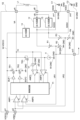
- ⁇ Configuration> 1 is a diagram showing an example of a power supply circuit 1 according to the present embodiment.
- the power supply circuit 1 is installed in an electronic device such as an active electrostatic stylus that can be equipped with a battery and can receive power from an external source, and supplies a potential to an electric circuit in the stylus.
- the power supply circuit 1 converts power supplied from a primary battery such as a dry cell, a secondary battery such as a lithium ion battery, and power supplied from an external power supply path such as an AC (alternating current) adapter or a USB (Universal Serial Bus) into power appropriate for the digital circuit, analog circuit, and LC oscillator circuit.
- the power supply circuit 1 then supplies the converted power to the digital circuit, analog circuit, and LC oscillator circuit.
- the power supply circuit 1 also charges a rechargeable secondary battery such as a lithium ion battery that is equipped with power supplied from outside.
- the power supply circuit 1 is configured to include, for example, a potential generating circuit 10, a boost circuit 20, constant voltage circuits 30, 60, 70, and 80, a charging circuit 40, and a band gap circuit 50.
- a potential generating circuit 10 for example, a boost circuit 20, constant voltage circuits 30, 60, 70, and 80, a charging circuit 40, and a band gap circuit 50.
- the device in which the power supply circuit 1 is mounted is not limited to a stylus, and may be any device having an electric circuit.
- the constant voltage circuit 30 is, for example, an LDO (Low Dropout) circuit, which converts the supplied potential to a constant potential of, for example, 4.0 V and outputs it. Specifically, the constant voltage circuit 30 converts the potential VIN supplied from an external power supply path such as a USB to a predetermined potential VDD33 based on the reference potential VREF supplied from the bandgap circuit 50. The constant voltage circuit 30 supplies the converted potential VDD33 to the power supply line W_VDD33 via the switch SW1.
- LDO Low Dropout
- the switch SW1 is, for example, a transistor or a mechanical switch, and shorts or opens between the constant voltage circuit 30 and the power supply line W_VDD33 based on the operation of the constant voltage circuit 30. Specifically, when the constant voltage circuit 30 is supplying potential VDD33 to the power supply line W_VDD33, the switch SW1 shorts between the constant voltage circuit 30 and the power supply line W_VDD33. In addition, when the constant voltage circuit 30 stops supplying potential VDD33 to the power supply line W_VDD33, the switch SW1 opens between the constant voltage circuit 30 and the power supply line W_VDD33.
- the charging circuit 40 is a circuit for supplying potential to a lithium-ion battery to charge it when the lithium-ion battery is used as the battery of a device in which the power supply circuit 1 is installed. Specifically, the charging circuit 40 converts the potential VDD33 supplied from the constant voltage circuit 30 via the power supply line W_VDD33 into a potential that can be charged into the lithium-ion battery, based on the reference potential VREF supplied from the band gap circuit 50. The charging circuit 40 charges the lithium-ion battery by supplying the converted potential to the lithium-ion battery via a path not shown.
- the boost circuit 20 is, for example, a boost DC-DC converter, and either boosts the supplied potential and outputs it, or outputs the supplied potential as is. Specifically, when a dry cell is used as the battery of the device in which the power supply circuit 1 is mounted, the boost circuit 20 boosts the potential VBAT of about 0.95V to about 1.60V supplied from the dry cell to about 2.1V based on the reference potential VREF supplied from the band gap circuit 50, and supplies the boosted potential to the power supply line W_VDD33 as potential VDD33.
- the boost circuit 20 supplies the potential VBAT of about 2.80V to about 4.40V supplied from the lithium ion battery to the power supply line W_VDD33 as potential VDD33 without boosting it.
- the bandgap circuit 50 is a standard for the operation of each circuit provided in the power supply circuit 1, and generates a reference potential VREF that is always constant regardless of temperature, power supply voltage, manufacturing process characteristics, etc., and supplies the generated reference potential VREF to each circuit.
- the bandgap circuit 50 uses the potential VDD33 supplied from the constant voltage circuit 30 or the boost circuit 20 via the power supply line W_VDD33 as a power source to generate the reference potential VREF, and supplies the generated reference potential VREF to each circuit.
- the potential generating circuit 10 is a DC-DC converter capable of generating multiple potentials, and generates a potential VDDD of approximately 1.4 V from the potential VDD33 supplied from the power supply line W_VDD33, a potential VDD2 of approximately 2.1 V, and a potential VR1 based on the potential VDD2, based on the reference potential VREF output from the bandgap circuit 50.
- the potential generating circuit 10 supplies the generated potential VDDD to each digital circuit in the power supply circuit 1.
- the potential generating circuit 10 also supplies the generated potential VDD2 to the constant voltage circuits 70 and 80.
- the potential generating circuit 10 also supplies the generated potential VR1 to the constant voltage circuit 60.
- the constant voltage circuit 60 is, for example, an LDO circuit, and converts the supplied potential to a predetermined potential and outputs it. Specifically, the constant voltage circuit 60 compares the magnitude of the reference potential VREF supplied from the band gap circuit 50 with the potential VR1 supplied from the potential generation circuit 10. When the potential of the reference potential VREF is equal to or higher than the potential VR1, the constant voltage circuit 60 generates a potential VDDD of 1.35V to 1.40V from the potential VDD33 supplied via the power supply line W_VDD33. The constant voltage circuit 30 then supplies the generated potential VDDD to each digital circuit in the power supply circuit 1. Furthermore, when the potential of the reference potential VREF is lower than the potential VR1, the constant voltage circuit 60 stops generating and outputting the potential VDDD.
- the constant voltage circuits 70 and 80 are, for example, LDO circuits, and convert the supplied potential to a predetermined potential and output it. Specifically, the constant voltage circuit 70 converts the potential VDD2 supplied from the potential generating circuit 10 to a potential VDDA of approximately 1.85 V based on the reference potential VREF supplied from the bandgap circuit 50. The constant voltage circuit 70 supplies the converted potential VDDA to each analog circuit in the power supply circuit 1. The constant voltage circuit 80 also converts the potential VDD2 supplied from the potential generating circuit 10 to a potential VDDLC of approximately 1.74 V to 2.055 V based on the reference potential VREF supplied from the bandgap circuit 50. The constant voltage circuit 80 supplies the converted potential VDDLC to each LC oscillation circuit in the power supply circuit 1.
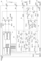
- FIG. 2 is a diagram showing an example of the potential generating circuit 10.
- the potential generating circuit 10 includes a control circuit 11, output circuits 12 to 14, amplifier circuits AMP1 to AMP4, buffer circuits BUF1 and BUF2, transistors TR1 to TR3, variable resistors R1 to R4, a constant voltage source V1, and a constant current source I1.
- An inductive element L1 having an inductance of about 22 ⁇ H is connected between terminals pA and pB of the potential generating circuit 10 via a signal line.
- a load capacitance C1 is connected to terminal po1 of the potential generating circuit 10 as a load capacitance of an electric circuit or electric element connected in a subsequent stage.
- a load capacitance C2 is connected to terminal po2 of the potential generating circuit 10 as a load capacitance of an electric circuit or electric element connected in a subsequent stage.
- the amplifier circuits AMP1 and AMP2 are, for example, comparators that determine whether the potential input to the non-inverting input terminal + is equal to or greater than the potential input to the inverting input terminal -, and transmit the determination result to the control circuit 11. Specifically, under the control of the control circuit 11, the amplifier circuit AMP1 determines whether the reference potential VREF input to the non-inverting input terminal + from the bandgap circuit 50 via the terminal pi2 is equal to or greater than the potential VR2, which is the divided potential of the variable resistors R3 and R4 input to the inverting input terminal -. The amplifier circuit AMP1 transmits the determination result to the control circuit 11.
- the amplifier circuit AMP2 determines whether the reference potential VREF input to the non-inverting input terminal + from the bandgap circuit 50 via the terminal pi2 is equal to or greater than the potential VR1, which is the divided potential of the variable resistors R1 and R2 input to the inverting input terminal -.
- the amplifier circuit AMP2 transmits the determination result to the control circuit 11.
- the control circuit 11 sends a signal to the buffer circuits BUF1 and BUF2 to cause the DC-DC converter formed by the buffer circuits BUF1 and BUF2 and the transistors TR1 and TR2 to output the potential VA or to stop the output of the potential VA.
- the control circuit 11 also operates the power supply circuit 1 in one of the first to fifth operating modes.
- the control circuit 11 controls the output circuits 12 and 13 to output a signal from one of the output circuits 12 and 13 in accordance with a combination of the magnitude relationship between the potential of the first signal SDDD output from the output circuit 12 and a predetermined first set potential, and the magnitude relationship between the potential of the second signal SDD2 output from the output circuit 13 and a predetermined second set potential.
- the control circuit 11 determines the magnitude relationship between the first signal SDDD and the first set potential based on the state of the output from the amplifier circuit AMP1.
- the control circuit 11 also determines the magnitude relationship between the second signal SDD2 and the second set potential based on the state of the output from the amplifier circuit AMP2. Note that the operation of the potential generating circuit 10 in each operating mode will be described later with reference to Figures 5A to 5E, and will not be described here.
- Buffer circuits BUF1 and BUF2 are buffer circuits comprised of, for example, MOS-FETs (metal-oxide-semiconductor field-effect transistors), which amplify the signal input to buffer circuit BUF1 while maintaining its logic, and output the augmented signal.
- buffer circuit BUF1 amplifies the signal input from control circuit 11 while maintaining its logic, and outputs the augmented signal to the gate terminal of transistor TR1.
- Buffer circuit BUF2 amplifies the signal input from control circuit 11 to buffer circuit BUF2 while maintaining its logic, and outputs the augmented signal to the gate terminal of transistor TR2.
- Transistors TR1 and TR3 are, for example, P-type MOS-FETs. Transistors TR1 and TR3 supply the potential supplied to their source terminals to their drain terminals or stop the supply in accordance with the signal input to their gate terminals. Specifically, when the state of the signal input to their gate terminals is low, transistors TR1 and TR3 supply the potential supplied to their source terminals to their drain terminals, but stop the supply when the potential of the signal input to their gate terminals is high.
- the gate terminal of transistor TR1 is connected to the output terminal of buffer circuit BUF1, the source terminal is connected to power supply line W_VDD33 via terminal pi1, and the drain terminal is connected to one end of inductive element L1 via node no and terminal pA.
- the gate terminal of the transistor TR3 is connected to the output terminal for the transistor TR3 of the control circuit 11, the source terminal is connected to the power supply line W_VDD33 via the terminal pi1, and the drain terminal is connected to the positive terminal of the constant current source I1 and the inverting input terminal - of the amplifier circuit AMP4.
- Transistor TR2 is, for example, an N-type MOS-FET. Transistor TR2 extracts charge from the drain terminal to the source terminal or stops the extraction according to a signal input to the gate terminal. Specifically, when the signal input to the gate terminal is in a high state, transistor TR2 extracts charge from the drain terminal to the source terminal, and when the signal input to the gate terminal is in a low state, transistor TR2 stops the extraction.
- the gate terminal of transistor TR2 is connected to the output terminal of buffer circuit BUF2, the source terminal is connected to the ground line W_GND, and the drain terminal is connected to one end of inductive element L1 via node no and terminal pA.
- the buffer circuits BUF1 and BUF2 and the transistors TR1 and TR2 function as a DC-DC converter.
- the DC-DC converter generates a potential VA by alternately switching the drain terminals and source terminals of the transistors TR1 and TR2 between conductive and non-conductive, and supplies the generated potential VA to the node no.
- the DC-DC converter supplies a potential VDD33 from the power line W_VDD33 to the node no via the transistor TR1.
- the DC-DC converter draws out a potential from the node no to the ground line W_GND via the transistor TR2.
- the constant voltage source V1 is a voltage source that generates a voltage so that the potential difference between the positive and negative terminals is a predetermined DC voltage, and supplies the generated DC voltage.
- the positive terminal of the constant voltage source V1 is connected to the non-inverting input terminal + of the amplifier circuit AMP3, and the negative terminal is connected to the node no.
- the constant current source I1 is a current source that generates a predetermined DC current so that the DC current flows from the positive terminal to the negative terminal under the control of the control circuit 11, and supplies the generated DC current.
- the positive terminal of the constant current source I1 is connected to the inverting input terminal - of the amplifier circuit AMP4 and the drain terminal of the transistor TR3, and the negative terminal is connected to the ground wire W_GND.
- the amplifier circuit AMP3 is, for example, a comparator, and performs zero-cross detection to detect the timing when the potential input to the non-inverting input terminal + exceeds or falls below the ground potential GND input to the inverting input terminal -. Specifically, under the control of the control circuit 11, the amplifier circuit AMP3 determines whether the potential input to the non-inverting input terminal + from the constant voltage source V1 is equal to or greater than the ground potential GND of the ground line W_GND input to the inverting input terminal -. The amplifier circuit AMP3 transmits the determination result to the control circuit 11.
- the amplifier circuit AMP4 is, for example, a comparator, and performs peak current detection to detect the timing at which the current flowing through the current path connected to the non-inverting input terminal + becomes equal to or exceeds a predetermined current flowing through the current path connected to the inverting input terminal -. Specifically, under the control of the control circuit 11, the amplifier circuit AMP4 determines whether the potential VA input from the drain terminals of transistors TR1 and TR2 to the non-inverting input terminal + is equal to or greater than the potential of the drain terminal of transistor TR3 and the positive terminal of constant current source I1 input to the inverting input terminal -. The amplifier circuit AMP4 transmits the determination result to the control circuit 11.
- the output circuit 12 outputs the potential VB supplied from the terminal pB as the first signal SDDD or stops the output based on the control of the control circuit 11.
- the output circuit 12 operates in one of the operation modes of the LDO mode, the DC-DC mode, and the standby mode. Details of the operation of the output circuit 12 in each operation mode will be explained later with reference to Figures 5A to 5E, so the explanation will be omitted here.
- the output circuit 13 outputs the potential VB supplied from the terminal pB as the second signal SDD2 or stops the output based on the control of the control circuit 11.
- the details of the operation of the output circuit 13 will be explained later with reference to Figures 5A to 5E, so the explanation will be omitted here.
- the output circuit 14 outputs the potential VDD33 supplied from the power supply line W_VDD33 as the second signal SDD2 or stops the output based on the control of the control circuit 11.
- the output circuit 14 operates in one of the operation modes of the current limit mode, the through mode, the DC-DC mode, and the standby mode. Details of the operation of the output circuit 14 in each operation mode will be explained later with reference to Figures 5A to 5E, so the explanation will be omitted here.
- variable resistors R1 to R4 are resistive elements whose resistance values at both ends can be changed.
- the resistance values of the variable resistors R1 to R4 are changed under the control of the control circuit 11.
- the variable resistors R1 and R2 function as a voltage divider circuit.
- the variable resistors R1 and R2 divide the potential VDDD output from the output circuit 12 using the resistance values of the variable resistors R1 and R2, outputting the divided potential VR1 to the inverting input terminal - of the amplifier circuit AMP2, and outputting the potential VR1 to the constant voltage circuit 60 via the terminal po3.
- One end of the variable resistor R1 is connected to the output terminal of the output circuit 12 and the terminal po1, and the other end is connected to one end of the variable resistor R2, the inverting input terminal - of the amplifier circuit AMP2, and the terminal po3.
- One end of the variable resistor R2 is connected to the other end of the variable resistor R1, the inverting input terminal - of the amplifier circuit AMP2, and the terminal po3, and the other end is connected to the ground line W_GND.
- the variable resistors R3 and R4 function as a voltage divider circuit.
- the variable resistors R3 and R4 divide the potential VDD2 output from the output circuit 13 or 14 using the resistance values of the variable resistors R3 and R4, and output the divided potential VR2 to the inverting input terminal - of the amplifier circuit AMP1.
- One end of the variable resistor R3 is connected to the output terminal of the output circuit 13, the output terminal of the output circuit 14, and the terminal po2, and the other end is connected to one end of the variable resistor R4 and the inverting input terminal - of the amplifier circuit AMP1.
- One end of the variable resistor R4 is connected to the other end of the variable resistor R3 and the inverting input terminal - of the amplifier circuit AMP1, and the other end is connected to the ground wire W_GND.
- FIG. 3 is a diagram showing an example of the configuration of the output circuits 12 to 14 together with other circuits in the potential generating circuit 10.
- the control circuit 11 includes, for example, an output control circuit 111 and a voltage control circuit 112.
- the output control circuit 111 controls the output circuits 12-14 and the switch SW10. Specifically, the output control circuit 111 transmits control signals CT121, CT122, CT124, and CT126 to the output circuit 12 to control the operation of the output circuit 12. The output control circuit 111 also transmits control signals CT131 and CT132 to the output circuit 13 to control the operation of the output circuit 13. The output control circuit 111 also transmits control signals CT142-CT144 to the output circuit 14 to control the operation of the output circuit 14. The output control circuit 111 also transmits an instruction to the voltage control circuit 112 to output the potential VA or to stop the output.
- the voltage control circuit 112 sends a signal to the buffer circuits BUF1 and BUF2 of the DC-DC converter formed by the buffer circuits BUF1 and BUF2 and the transistors TR1 and TR2 in accordance with the instructions transmitted from the output control circuit 111 so that the DC-DC converter outputs the potential VA or stops the output.
- the output circuit 12 includes, for example, transistors TR121 to TR127 and a buffer circuit BUF121.
- the output circuit 12 and the control circuit 11 form a backflow prevention circuit 15.
- the buffer circuit BUF121 is a buffer circuit including, for example, a MOS-FET, which amplifies the input signal while maintaining its logic, and outputs the amplified signal. Specifically, the buffer circuit BUF121 amplifies the control signal CT121 sent from the output control circuit 111 while maintaining its logic, and outputs the amplified signal to the gate terminal of transistor TR121 and the source terminal of transistor TR122.
- Transistors TR121 to TR127, TR131 to TR133, TR141 to TR143, TR145 and TR146 are, for example, P-type MOS-FETs. Transistors TR121 to TR127, TR131 to TR133, TR141 to TR143, TR145 and TR146 supply the potential supplied to their source terminals to their drain terminals or stop the supply in accordance with a signal input to their gate terminals. Specifically, when the state of the signal input to their gate terminals is low, transistors TR121 to TR127, TR131 to TR133, TR141 to TR143, TR145 and TR146 supply the potential supplied to their source terminals to their drain terminals, while stopping the supply when the potential of the signal input to their gate terminals is high. In addition, the back gate terminals of transistors TR122 to TR127, TR131 to TR133, TR141 to TR143, TR145, and TR146, except for transistor TR121, are connected to the source terminals.
- the gate terminal of transistor TR121 is connected to the output terminal of buffer circuit BUF121 and the source terminal of transistor TR122, and the source terminal is connected to the other end of inductive element L1 via terminal pB, as well as to the source terminal of transistor TR124, the drain terminal of transistor TR131, and one end of switch SW10.
- the drain terminal of transistor TR121 is connected to one end of load capacitance C1 via terminal po1, as well as to the source terminals of transistors TR123 and TR127, and the backgate terminal is connected to the source terminals of transistors TR124 and TR126.
- Transistor TR122 has a gate terminal to which a control signal CT122 sent from the output control circuit 111 is input.
- the source terminal of transistor TR122 is connected to the gate terminal of transistor TR121 and the output terminal of buffer circuit BUF121, and the drain terminal is connected to the drain terminal of transistor TR123.
- the control signal CT122 transmitted from the output control circuit 111 is input to the gate terminal of the transistor TR123.
- the source terminal of the transistor TR123 is connected to one end of the load capacitance C1 via the terminal po1, and is also connected to the drain terminal of the transistor TR121 and the source terminal of the transistor TR127, and the drain terminal is connected to the drain terminal of the transistor TR122.
- Transistor TR124 receives a control signal CT124 sent from the output control circuit 111 at its gate terminal.
- the source terminal of transistor TR124 is connected to the other end of inductive element L1 via terminal pB, and is also connected to the source terminal of transistor TR121, the drain terminal of transistor TR131, and one end of switch SW10.
- the drain terminal of transistor TR124 is connected to the drain terminal of transistor TR125.
- Transistor TR124 and transistor TR125 form a first short-circuit control circuit.
- Transistor TR125 has a gate terminal to which a control signal CT124 transmitted from the output control circuit 111 is input.
- transistor TR125 has a source terminal connected to the back gate terminal of transistor TR121 and the source terminal of transistor TR126, and a drain terminal connected to the drain terminal of transistor TR124.
- Transistor TR125 and transistor TR124 form a first short-circuit control circuit.
- Transistor TR126 has a gate terminal to which a control signal CT126 transmitted from the output control circuit 111 is input.
- transistor TR126 has a source terminal connected to the back gate terminal of transistor TR121 and the source terminal of transistor TR125, and a drain terminal connected to the drain terminal of transistor TR127.
- Transistor TR126 and transistor TR127 form a second short-circuit control circuit.
- Transistor TR127 has a gate terminal to which a control signal CT126 transmitted from the output control circuit 111 is input.
- the source terminal of transistor TR127 is connected to one end of the load capacitance C1 via terminal po1, and is also connected to the drain terminal of transistor TR121 and the source terminal of transistor TR123, and the drain terminal is connected to the drain terminal of transistor TR126.
- Transistor TR127 and transistor TR126 form a second short-circuit control circuit.
- the output circuit 13 includes, for example, transistors TR131 to TR133 and a buffer circuit BUF131.
- the buffer circuit BUF131 is a buffer circuit including, for example, a MOS-FET, which amplifies the input signal while maintaining its logic, and outputs the amplified signal. Specifically, the buffer circuit BUF131 amplifies the control signal CT131 sent from the output control circuit 111 while maintaining its logic, and outputs the amplified signal to the gate terminal of transistor TR131 and the source terminal of transistor TR132.
- the gate terminal of transistor TR131 is connected to the output terminal of buffer circuit BUF131 and the source terminal of transistor TR132.
- the source terminal of transistor TR131 is connected to one end of load capacitance C2 via terminal po2 and to the source terminals of transistors TR133, TR141, and TR146.
- the drain terminal of transistor TR131 is connected to the other end of inductive element L1 via terminal pB and is connected to the source terminals of transistors TR121 and TR124 and one end of switch SW10.
- the control signal CT132 transmitted from the output control circuit 111 is input to the gate terminal of the transistor TR132.
- the source terminal of the transistor TR132 is connected to the output terminal of the buffer circuit BUF131 and the gate terminal of the transistor TR131.
- the drain terminal of the transistor TR132 is connected to the drain terminal of the transistor TR133.
- Transistor TR133 has a gate terminal to which a control signal CT132 transmitted from the output control circuit 111 is input.
- the source terminal of transistor TR133 is connected to one end of load capacitance C2 via terminal po2, and is also connected to the source terminals of transistors TR131, TR141, and TR146.
- the drain terminal of transistor TR133 is connected to the drain terminal of transistor TR132.
- the output circuit 14 includes, for example, transistors TR141 to TR146.
- the gate terminal of transistor TR141 is connected to the source terminals of transistors TR144 and TR145.
- the source terminal of transistor TR141 is connected to one end of load capacitance C2 via terminal po2, and is also connected to the source terminals of transistors TR131, TR133, and TR146.
- the drain terminal of transistor TR141 is connected to the drain terminals of transistors TR142 and TR143.
- Transistor TR142 has a gate terminal to which a control signal CT142 sent from the output control circuit 111 is input.
- the source terminal of transistor TR142 is connected to the power supply line W_VDD33 via terminal pi1, and is also connected to the source terminals of transistors TR1 and TR143.
- the drain terminal of transistor TR142 is connected to the drain terminals of transistors TR141 and TR143.
- Transistor TR143 has a gate terminal to which a control signal CT143 sent from the output control circuit 111 is input.
- the source terminal of transistor TR143 is connected to the power supply line W_VDD33 via terminal pi1, and is also connected to the source terminals of transistors TR1 and TR142.
- the drain terminal of transistor TR143 is connected to the drain terminals of transistors TR141 and TR142.
- Transistor TR144 is, for example, an N-type MOS-FET. Transistor TR144 extracts charge from the drain terminal to the source terminal or stops the extraction according to a signal input to the gate terminal. Specifically, when the signal input to the gate terminal is in a high state, transistor TR144 extracts charge from the drain terminal to the source terminal, and when the signal input to the gate terminal is in a low state, transistor TR144 stops the extraction. Specifically, a control signal CT144 transmitted from the output control circuit 111 is input to the gate terminal of transistor TR144. The source terminal of transistor TR144 is connected to the source terminal of transistor TR145 and the gate terminal of TR141. The drain terminal of transistor TR144 is connected to the ground line W_GND.
- Transistor TR145 has a gate terminal to which a control signal CT144 transmitted from the output control circuit 111 is input.
- transistor TR145 has a source terminal connected to the source terminal of transistor TR144 and the gate terminal of TR141.
- transistor TR145 has a drain terminal connected to the drain terminal of transistor TR146.
- Transistor TR146 has a gate terminal to which a control signal CT144 transmitted from the output control circuit 111 is input.
- the source terminal of transistor TR146 is connected to one end of the load capacitance C2 via terminal po2, and is also connected to the source terminals of transistors TR131, TR133, and TR144.
- the drain terminal of transistor TR146 is connected to the drain terminal of transistor TR145.
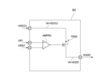
- FIG. 4 is a diagram showing an example of the constant voltage circuit 60.
- the constant voltage circuit 60 includes, for example, an amplifier circuit AMP60 and a transistor TR60.
- the amplifier circuit AMP60 is, for example, a comparator that determines whether the potential input to the non-inverting input terminal + is equal to or greater than the potential input to the inverting input terminal -, and outputs the determination result to the transistor TR60. Specifically, the amplifier circuit AMP60 determines whether the potential VR1 input to the non-inverting input terminal + from the potential generating circuit 10 is equal to or greater than the reference potential VREF input to the inverting input terminal - from the band gap circuit 50. If the determination result is a positive determination, the amplifier circuit AMP60 outputs a high-state signal to the gate terminal of the transistor TR60. If the determination result is a negative determination, the amplifier circuit AMP60 outputs a low-state signal to the gate terminal of the transistor TR60.
- Transistor TR60 is, for example, a P-type MOS-FET. Transistor TR60 makes the source terminal and drain terminal conductive or non-conductive according to the potential input to the gate terminal. Specifically, when the state of the signal input to the gate terminal is low, transistor TR60 makes the source terminal and drain terminal conductive, while when the potential of the signal input to the gate terminal is high, transistor TR60 makes the source terminal and drain terminal non-conductive. When transistor TR60 has conductivity between the source terminal and drain terminal, it supplies from the drain terminal a potential that is a voltage drop from the potential supplied to the source terminal by an amount equal to the potential difference according to the source-drain resistance.
- the transistor TR60 has a gate terminal connected to the output terminal of the amplifier circuit AMP60, a source terminal connected to the power supply line W_VDD33, and a drain terminal connected to the power supply line W_VDDD.
- the configuration of the power supply circuit 1 has been described above. Next, the operation of the power supply circuit 1 in each mode will be described in detail.
- the output circuit 12 in the power supply circuit 1 operates in any one of the operation modes of the LDO mode, the DC-DC mode, and the standby mode.
- the output circuit 14 in the power supply circuit 1 operates in any one of the operation modes of the current limit mode, the through mode, the DC-DC mode, and the standby mode.
- the power supply circuit 1 switches its operation depending on whether the device in which the power supply circuit 1 is mounted is equipped with a dry cell battery or a lithium ion battery. A case will be described where the device in which the power supply circuit 1 is mounted is equipped with a dry cell mode. After starting up the power supply circuit 1, the power supply circuit 1 first operates the output circuit 12 in LDO mode, and then operates it in DC-DC mode. After starting up the power supply circuit 1, the power supply circuit 1 also first operates the output circuit 14 in current limit mode, and then operates it in through mode. Furthermore, when the device in which the power supply circuit 1 is mounted is in a sleep state, the power supply circuit 1 also operates the output circuits 12 to 14 in standby mode.
- the power supply circuit 1 After starting up the power supply circuit 1, the power supply circuit 1 first operates the output circuit 12 in LDO mode, and then operates it in DC-DC mode. After starting up the power supply circuit 1, the power supply circuit 1 first operates the output circuit 14 in current limit mode for a predetermined time, and then operates it in through mode while the output circuit 12 is operating in LDO mode. Furthermore, when the output circuit 12 switches its operating mode from LDO mode to DC-DC mode, the power supply circuit 1 switches the operating mode of the output circuit 14 from through mode to DC-DC mode, and operates the output circuit 14 in DC-DC mode. Furthermore, when the device equipped with the power supply circuit 1 is in a sleep state, the power supply circuit 1 operates the output circuits 12 to 14 in standby mode.
- FIG. 5A is a diagram showing an example of the operation of the potential generating circuit 10 in the first mode.
- the state in which the source terminal and the drain terminal of the transistor are conductive is called the ON state
- the state in which the source terminal and the drain terminal of the transistor are non-conductive is called the OFF state.
- the voltage control circuit 112 in the control circuit 11 controls the operation of the DC-DC converter formed by the transistors TR1 and TR2 and the buffer circuits BUF1 and BUF2 so as to stop the generation of the potential VA.
- the output control circuit 111 transitions the potential of the terminal pB to the ground potential GND by short-circuiting the switch SW10.
- the output control circuit 111 in the control circuit 11 transmits a control signal CT121 to the buffer circuit BUF121 so that the state of the signal output from the buffer circuit BUF121 becomes a high impedance state.
- the output control circuit 111 also transmits a low state control signal CT122 to the gate terminals of the transistors TR122 and TR123, and sets the transistors TR122 and TR123 to the on state.
- the output control circuit 111 also transmits a low state control signal CT126 to the gate terminals of the transistors TR126 and TR127, and sets the transistors TR126 and TR127 to the on state.
- the output control circuit 111 also transmits a high state control signal CT124 to the gate terminals of the transistors TR124 and TR125, and sets the transistors TR124 and TR125 to the off state.
- the gate terminal of transistor TR121 is supplied with potential VDDD from the constant voltage circuit 60 via on-state transistors TR122 and TR123 and terminal po1. Also in the first mode, the source terminal of transistor TR121 is supplied with ground potential GND via switch SW10. Also in the first mode, the drain terminal of transistor TR121 is supplied with potential VDDD from the constant voltage circuit 60 via terminal po1. Furthermore, the backgate terminal of transistor TR121 is supplied with potential VDDD from the constant voltage circuit 60 via on-state transistors TR126 and TR127 and terminal po1.
- transistor TR121 is turned off in accordance with the states of transistors TR122 to TR127. Also, in the first mode, the backgate terminal of transistor TR121 is connected to the drain terminal via transistors TR126 and TR127, forming a parasitic diode from the source terminal to the drain terminal via the backgate terminal. In the first mode, transistor TR121 is conductive in the direction from the source terminal to the drain terminal, but is non-conductive in the direction from the drain terminal to the source terminal.
- the backflow prevention circuit 15 including the output circuit 12 and the control circuit 11 is in a first state in which the ground potential GND is supplied to the source terminal.
- the reverse current prevention circuit 15 prevents current from flowing from the input side to the output side of the output circuit 12 because the parasitic diode is conductive in the direction from the input side to the output side of the output circuit 12, but the potential of the output side terminal po1 is higher than the potential of the input side terminal pB. Also, in the first state, the reverse current prevention circuit 15 prevents current from flowing back from the output side to the input side because the parasitic diode is not conductive in the direction from the output side to the input side of the output circuit 12.
- the output control circuit 111 in the control circuit 11 sends a control signal CT131 to the buffer circuit BUF131 so that the state of the signal output from the buffer circuit BUF131 becomes a high impedance state.
- the output control circuit 111 sends a low state control signal CT132 to the gate terminals of the transistors TR132 and TR133, setting the transistors TR132 and TR133 to the on state.
- the gate terminal of the transistor TR131 is supplied with a potential VDD2 from the output circuit 14 via the transistors TR132 and TR133 that are in the on state. Also in the first mode, the source terminal of the transistor TR131 is supplied with a potential VDD2 from the output circuit 14. Also in the first mode, the drain terminal of the transistor TR131 is supplied with a ground potential GND via the switch SW10.
- transistor TR131 is turned off in accordance with the states of transistors TR132 and TR133.
- the back gate terminal of transistor TR131 is connected to the source terminal, a parasitic diode is formed from the drain terminal to the source terminal via the back gate terminal.
- Transistor TR131 is conductive in the direction from the drain terminal to the source terminal, but is non-conductive in the direction from the source terminal to the drain terminal.
- the parasitic diode of the output circuit 13 is conductive in the direction from the input side to the output side, the potential of the output side terminal po2 is higher than the potential of the input side terminal pB, so current is prevented from flowing from the input side to the output side of the output circuit 13. Also, in the first mode, the parasitic diode of the output circuit 13 is not conductive in the direction from the output side to the input side, so current is prevented from flowing back from the output side to the input side.
- the output control circuit 111 in the control circuit 11 sends a high-state control signal CT144 to the gate terminals of transistors TR144 to TR146, setting transistor TR144 to an on state and transistors TR145 and TR146 to an off state.
- the gate terminal of transistor TR141 is supplied with ground potential GND from transistor TR144, which is in an on state, via the ground line W_GND, and the transistor TR141 is turned on. Note that, in the first mode, the back gate terminal of transistor TR146 is connected to the source terminal, thereby preventing current from flowing in the direction from the source terminal to the drain terminal.
- the output control circuit 111 When the power supply circuit 1 is in the first mode and the output circuit 14 is in the current limiting mode, the output control circuit 111 sends a high-state control signal CT142 to the gate terminal of transistor TR142 to set transistor TR142 to the off state. When the power supply circuit 1 is in the first mode and the output circuit 14 is in the current limiting mode, the output control circuit 111 sends a low-state control signal CT143 to the gate terminal of transistor TR143 to set transistor TR143 to the on state.
- the output circuit 14 when the power supply circuit 1 is in the first mode and the output circuit 14 is in the current limiting mode, the output circuit 14 outputs a potential VDD2 from the power supply line W_VDD33 via the transistors TR143 and TR141 in the on state so that the potential VDD2 is approximately the same as the potential VDD33 of the power supply line W_VDD33. Since the on resistance of the transistor TR143 is greater than the on resistance of the transistor TR142, the output circuit 14 outputs a potential VDD2 to the terminal po2 in the current limiting mode so that the output current is smaller than when the output circuit 14 is operating in the through mode.
- the output control circuit 111 When the power supply circuit 1 is in the first mode and the output circuit 14 is in the through mode, the output control circuit 111 sends a low-state control signal CT142 to the gate terminal of transistor TR142, setting transistor TR142 to the on state. When the power supply circuit 1 is in the first mode and the output circuit 14 is in the through mode, the output control circuit 111 sends a high-state control signal CT143 to the gate terminal of transistor TR143, setting transistor TR143 to the off state.
- the output circuit 14 when the power supply circuit 1 is in the first mode and the output circuit 14 is in the through mode, the output circuit 14 outputs a potential VDD2 from the power supply line W_VDD33 via the transistors TR142 and TR141 in the on state so that the potential VDD2 is approximately the same as the potential VDD33 of the power supply line W_VDD33. Since the on resistance of the transistor TR142 is smaller than the on resistance of the transistor TR143, the output circuit 14 outputs a potential VDD2 to the terminal po2 in the through mode so that the output current is greater than when the output circuit 14 is operating in the current limit mode.
- FIG. 5B is a diagram showing an example of the operation of the potential generating circuit 10 in the second mode.
- the voltage control circuit 112 in the control circuit 11 controls the operation of the DC-DC converter formed by the transistors TR1 and TR2 and the buffer circuits BUF1 and BUF2 so as to generate the potential VA.
- the output control circuit 111 also controls the switch SW10 to be open, thereby preventing the terminal pB from being connected to the ground line W_GND.
- the output control circuit 111 in the control circuit 11 transmits a control signal CT121 to the buffer circuit BUF121 so that the state of the signal output from the buffer circuit BUF121 becomes a low state.
- the output control circuit 111 also transmits a high-state control signal CT122 to the gate terminals of the transistors TR122 and TR123, and sets the transistors TR122 and TR123 to an off state.
- the output control circuit 111 also transmits a high-state control signal CT126 to the gate terminals of the transistors TR126 and TR127, and sets the transistors TR126 and TR127 to an off state.
- the output control circuit 111 also transmits a low-state control signal CT124 to the gate terminals of the transistors TR124 and TR125, and sets the transistors TR124 and TR125 to an on state.
- the backflow prevention circuit 15 including the control circuit 11 and the output circuit 12 is in the second state in which the potential VB is supplied to the source terminal.
- the backflow prevention circuit 15 has a parasitic diode formed from the drain terminal of the transistor TR121 toward the source terminal via the backgate terminal by connecting the backgate terminal of the transistor TR121 to the source terminal via the transistors TR124 and TR125.
- the output control circuit 111 in the control circuit 11 sends a control signal CT131 to the buffer circuit BUF131 so that the state of the signal output from the buffer circuit BUF131 becomes a high state.
- the output control circuit 111 sends a high-state control signal CT132 to the gate terminals of the transistors TR132 and TR133, setting the transistors TR132 and TR133 to an off state.
- a high-state signal is input to the gate terminal of the transistor TR131 from the buffer circuit BUF131. Also in the second mode, the source terminal of the transistor TR131 is supplied with the potential VDD2 from the output circuit 14. Also in the second mode, the drain terminal of the transistor TR131 is supplied with the potential VB of the terminal pB.
- transistor TR131 is turned off in accordance with the states of transistors TR132 and TR133.
- transistor TR131 since the back gate terminal of transistor TR131 is connected to the source terminal, a parasitic diode is formed from the drain terminal to the source terminal via the back gate terminal.
- Transistor TR131 is conductive in the direction from the drain terminal to the source terminal, but is non-conductive in the direction from the source terminal to the drain terminal.
- the parasitic diode of the output circuit 13 is conductive in the direction from the input side to the output side, the potential of the output side terminal po2 is higher than the potential of the input side terminal pB, so current is prevented from flowing from the input side to the output side of the output circuit 13. Also, in the second mode, the parasitic diode of the output circuit 13 is not conductive in the direction from the output side to the input side, so current is prevented from flowing back from the output side to the input side.
- the output control circuit 111 in the control circuit 11 sends a high-state control signal CT144 to the gate terminals of transistors TR144 to TR146, setting transistor TR144 to the on state and transistors TR145 and TR146 to the off state.
- the output control circuit 111 also sends a low-state control signal CT142 to the gate terminal of transistor TR142, setting transistor TR142 to the on state.
- the output control circuit 111 also sends a high-state control signal CT143 to the gate terminal of transistor TR143, setting transistor TR143 to the off state.
- the output circuit 14 outputs a second signal SDD2 from the power supply line W_VDD33 via the on-state transistors TR142 and TR141 so that the potential VDD2 is approximately the same as the potential VDD33 of the power supply line W_VDD33.
- the back gate terminal of transistor TR146 is connected to the source terminal, thereby preventing current from flowing in the direction from the source terminal to the drain terminal.
- FIG. 5C is a diagram showing an example of the operation of the potential generating circuit 10 in the third mode.
- the voltage control circuit 112 in the control circuit 11 controls the operation of the DC-DC converter formed by the transistors TR1 and TR2 and the buffer circuits BUF1 and BUF2 so as to generate the potential VA.
- the output control circuit 111 controls the switch SW10 to be open, thereby preventing the terminal pB from being connected to the ground line W_GND.
- the output control circuit 111 in the control circuit 11 transmits a control signal CT121 to the buffer circuit BUF121 so that the state of the signal output from the buffer circuit BUF121 becomes a high state.
- the output control circuit 111 also transmits a high state control signal CT122 to the gate terminals of the transistors TR122 and TR123, and sets the transistors TR122 and TR123 to an off state.
- the output control circuit 111 also transmits a high state control signal CT126 to the gate terminals of the transistors TR126 and TR127, and sets the transistors TR126 and TR127 to an off state.
- the output control circuit 111 also transmits a low state control signal CT124 to the gate terminals of the transistors TR124 and TR125, and sets the transistors TR124 and TR125 to an on state.
- a high-state signal is input to the gate terminal of transistor TR121 from buffer circuit BUF121.
- a potential VB is supplied to the source terminal of transistor TR121 via terminal pB.
- a potential VDDD is supplied to the drain terminal of transistor TR121 from constant voltage circuit 60 via terminal po1.
- a potential VB is supplied to the backgate terminal of transistor TR121 via transistors TR124 and TR125 that are in the on state and terminal pB.
- transistor TR121 is turned off in accordance with the states of transistors TR122 to TR127. Also, in the third mode, the backgate terminal of transistor TR121 is connected to the source terminal via transistors TR124 and TR125, forming a parasitic diode from the drain terminal to the source terminal via the backgate terminal. In the third mode, transistor TR121 is conductive in the direction from the drain terminal to the source terminal, but is non-conductive in the direction from the source terminal to the drain terminal.
- the backflow prevention circuit 15 including the control circuit 11 and the output circuit 12 is in a second state in which the source terminal is supplied with the potential VB.
- the backflow prevention circuit 15 prevents current from flowing from the output side to the input side of the output circuit 12 because the parasitic diode is conductive in the direction from the output side to the input side of the output circuit 12, but the potential of the terminal pB on the input side is higher than the potential of the terminal po1 on the output side.
- the backflow prevention circuit 15 prevents current from flowing back from the input side to the output side because the parasitic diode is not conductive in the direction from the input side to the output side of the output circuit 12.
- the output control circuit 111 in the control circuit 11 sends a control signal CT131 to the buffer circuit BUF131 so that the state of the signal output from the buffer circuit BUF131 becomes high.
- the output control circuit 111 also sends a high-state control signal CT132 to the gate terminals of the transistors TR132 and TR133, setting the transistors TR132 and TR133 to the off state. Note that the operation of the output circuit 13 in the third mode is the same as in the second mode, so a description thereof will be omitted.
- the output control circuit 111 in the control circuit 11 sends a high-state control signal CT144 to the gate terminals of transistors TR144 to TR146, setting transistor TR144 to an on state and transistors TR145 and TR146 to an off state.
- the output control circuit 111 When the power supply circuit 1 is in the third mode and the output circuit 14 is in the current limiting mode, the output control circuit 111 sends a high-state control signal CT142 to the gate terminal of the transistor TR142 to set the transistor TR142 to the off state. When the power supply circuit 1 is in the third mode and the output circuit 14 is in the current limiting mode, the output control circuit 111 sends a low-state control signal CT143 to the gate terminal of the transistor TR143 to set the transistor TR143 to the on state.
- the output control circuit 111 sends a low-state control signal CT142 to the gate terminal of the transistor TR142 to set the transistor TR142 to the on state.
- the output control circuit 111 sends a low-state control signal CT143 to the gate terminal of the transistor TR143 to set the transistor TR143 to the off state.
- the back gate terminal of the transistor TR146 is connected to the source terminal, so that in the first mode, a current does not flow in the direction from the source terminal to the drain terminal.
- the operation of the output circuit 14 in the third mode is the same as in the first mode, so a description thereof will be omitted.
- FIG. 5D is a diagram showing an example of the operation of the potential generating circuit 10 in the fourth mode.
- the voltage control circuit 112 in the control circuit 11 controls the operation of the DC-DC converter formed by the transistors TR1 and TR2 and the buffer circuits BUF1 and BUF2 so as to generate the potential VA.
- the output control circuit 111 controls the switch SW10 to be open, thereby preventing the terminal pB from being connected to the ground line W_GND.
- the output control circuit 111 in the control circuit 11 sends a control signal CT121 to the buffer circuit BUF121 so that the state of the signal output from the buffer circuit BUF121 becomes a low state.
- the output control circuit 111 also sends a high-state control signal CT122 to the gate terminals of the transistors TR122 and TR123, setting the transistors TR122 and TR123 to an off state.
- the output control circuit 111 also sends a high-state control signal CT126 to the gate terminals of the transistors TR126 and TR127, setting the transistors TR126 and TR127 to an off state.
- the output control circuit 111 also sends a low-state control signal CT124 to the gate terminals of the transistors TR124 and TR125, setting the transistors TR124 and TR125 to an on state.
- the states of the transistor TR121, the output circuit 12, and the backflow prevention circuit 15 in the fourth mode are the same as in the second mode, so their explanation will be omitted.
- the output control circuit 111 in the control circuit 11 sends a control signal CT131 to the buffer circuit BUF131 so that the state of the signal output from the buffer circuit BUF131 becomes low.
- the output control circuit 111 sends a high-state control signal CT132 to the gate terminals of the transistors TR132 and TR133, setting the transistors TR132 and TR133 to the off state.
- a low-state signal is input to the gate terminal of the transistor TR131 from the buffer circuit BUF131, and the transistor TR131 is turned on. Also, in the fourth mode, the output circuit 13 receives the potential VB of the terminal pB at the drain terminal of the transistor TR131, and outputs a second signal SDD2 with a potential VDD2 from the source terminal of the transistor TR131 via the terminal po2.
- the output control circuit 111 in the control circuit 11 sends a low-state control signal CT144 to the gate terminals of transistors TR144 to TR146, turning off transistor TR144 and turning on transistors TR145 and TR146.
- the output control circuit 111 also sends a high-state control signal CT142 to the gate terminal of transistor TR142, turning off transistor TR142.
- the output control circuit 111 also sends a high-state control signal CT143 to the gate terminal of transistor TR143, turning off transistor TR143. Note that the back gate terminals of transistors TR142 to TR144 are connected to the source terminals, preventing current from flowing from the source terminals to the drain terminals in the fourth mode.
- the gate terminal of transistor TR141 is supplied with potential VDD from terminal po2 via transistors TR145 and TR146, which are in the on state.
- transistor TR141 is in the on state when the potential of potential VDD2 is lower than the potential of the drain terminal of transistor TR141.
- transistors TR142 and TR143 prevent current from flowing from power line W_VDD33 to terminal po2 via transistor TR141, which is in the on state, because the conduction direction of the parasitic diode is from the drain terminal to the source terminal.
- transistor TR141 when the potential of potential VDD2 is higher than the potential of the drain terminal of transistor TR141, transistor TR141 is turned off. In the fourth mode and when transistor TR141 is turned off, the direction of conduction of the parasitic diode of transistor TR141 is from the drain terminal to the source terminal, so that current is prevented from flowing from terminal po2 to power line W_VDD33 via the parasitic diodes of transistors TR142 and TR143.
- FIG. 5E is a diagram showing an example of the operation of the potential generating circuit 10 in the fifth mode.
- the voltage control circuit 112 in the control circuit 11 controls the operation of the DC-DC converter formed by the transistors TR1 and TR2 and the buffer circuits BUF1 and BUF2 so as to stop the generation of the potential VA.
- the output control circuit 111 transitions the potential of the terminal pB to the ground potential GND, which is the potential of the ground line W_GND, by short-circuiting the switch SW10.
- the output control circuit 111 in the control circuit 11 transmits a control signal CT121 to the buffer circuit BUF121 so that the state of the signal output from the buffer circuit BUF121 becomes a high impedance state.
- the output control circuit 111 also transmits a low state control signal CT122 to the gate terminals of the transistors TR122 and TR123, and sets the transistors TR122 and TR123 to the on state.
- the output control circuit 111 also transmits a low state control signal CT126 to the gate terminals of the transistors TR126 and TR127, and sets the transistors TR126 and TR127 to the on state.
- the output control circuit 111 also transmits a high state control signal CT124 to the gate terminals of the transistors TR124 and TR125, and sets the transistors TR124 and TR125 to the off state.
- the gate terminal of the transistor TR121 is supplied with the potential VDDD from the constant voltage circuit 60 via the on-state transistors TR122 and TR123 and the terminal po1.
- the source terminal of the transistor TR121 is supplied with the ground potential GND via the switch SW10.
- the drain terminal of the transistor TR121 is supplied with the potential VDDD from the constant voltage circuit 60 via the terminal po1.
- the backgate terminal of the transistor TR121 is supplied with the potential VDDD via the on-state transistors TR126 and TR127 and the terminal po1. Note that the states of the transistor TR121 and the backflow prevention circuit 15 in the fifth mode are the same as those in the first mode, so a description thereof will be omitted.
- the output control circuit 111 in the control circuit 11 sends a control signal CT131 to the buffer circuit BUF131 so that the state of the signal output from the buffer circuit BUF131 becomes a high impedance state.
- the output control circuit 111 sends a low state control signal CT132 to the gate terminals of the transistors TR132 and TR133, setting the transistors TR132 and TR133 to the off state.
- the gate terminal of the transistor TR131 is supplied with the potential VDD2 from the output circuit 14 via the transistors TR132 and TR133 that are in the on state. Also, in the fifth mode, the source terminal of the transistor TR131 is supplied with the potential VDD2 from the terminal po2. Also, in the fifth mode, the drain terminal of the transistor TR131 is supplied with the ground potential GND via the switch SW10. Note that the operation of the output circuit 13 in the fifth mode is the same as in the first mode, so a description thereof will be omitted.
- the output control circuit 111 in the control circuit 11 sends a low-state control signal CT144 to the gate terminals of transistors TR144 to TR146, setting transistor TR144 to an off state and transistors TR145 and TR146 to an on state.
- the output control circuit 111 also sends a high-state control signal CT142 to the gate terminal of transistor TR142, setting transistor TR142 to an off state.
- the output control circuit 111 also sends a high-state control signal CT143 to the gate terminal of transistor TR143, setting transistor TR143 to an off state.
- the back gate terminals of transistors TR142 to TR144 are connected to the source terminals, thereby preventing current from flowing from the source terminals to the drain terminals. Also, the operation of the output circuit 14 in the fifth mode is the same as in the fourth mode, so a description thereof will be omitted.
- FIG. 6A is a first example of a timing chart showing the output state of the potential generating circuit 10.
- FIG. 6B is a second example of a timing chart showing the output state of the potential generating circuit 10.
- the control circuit 11 sets the operation mode of the power supply circuit 1 to the fourth mode, the first set potential to 1.4 V, and the second set potential to 2.1 V.
- the control circuit 11 sets the operation mode of the power supply circuit 1 to the fourth mode, the first set potential to 1.4 V, and the second set potential to 2.1 V.
- the control circuit 11 controls the states of the control signals CT121 and CT131 so that the output circuits 12 and 13 alternately output the control signals at regular intervals.
- the control circuit 11 stops the output from the output circuit 13 and controls the states of the control signals CT121 and CT131 to perform an output from the output circuit 12.
- the control circuit 11 stops the output by the output circuit 12 and controls the states of the control signals CT121 and CT131 to output from the output circuit 13.
- the control circuit 11 controls the states of the control signals CT121 and CT131 to output from only one of the output circuits 12 and 14.
- FIG. 7 is a first example of a timing chart showing the transition of each signal in the potential generating circuit 10.
- the device in which the power supply circuit 1 is mounted is equipped with a dry cell as a battery, and the power supply circuit 1 operates by switching between a first mode, a second mode, and a fifth mode.
- the first set potential is set to 1.4V.
- the second set potential is set to 2.1V.
- the control circuit 11 sets the operating mode of the power supply circuit 1 to the first mode, and sets the output circuit 14 to the current limiting mode. Specifically, the control circuit 11 sets the states of the control signals CT121 and CT131 to a high impedance state. The control circuit 11 also sets the states of the control signals CT122, CT126, CT132, CT142, and CT144 to a high state. The control circuit 11 also sets the states of the control signals CT124 and CT143 to a low state. The control circuit 11 outputs each control signal whose state has been set.
- the output circuit 12 operates in LDO mode and stops outputting the potential VDDD.
- a potential is supplied to the terminal po1 by the constant voltage circuit 60, and the potential VDDD starts to transition to the first set potential of 1.4 V.
- the output circuit 13 stops outputting the potential VDD2.
- the output circuit 14 also operates in a current limiting mode, and outputs the potential of the power supply line W_VDD33 to the terminal po2 while suppressing the inrush current.
- the potential VDD2 of the terminal po2 starts to transition to the second set potential of 2.1 V.
- the control circuit 11 sets the output circuit 14 to the through mode. Specifically, the control signals CT132 and CT142 transition to a low state. In addition, the control circuit 11 transitions the state of the control signal CT143 to a high state.
- the output circuit 12 operates in LDO mode and stops outputting the potential VDDD.
- a potential is supplied to the terminal po1 by the constant voltage circuit 60, and the potential VDDD reaches the first set potential of 1.4 V.
- the output circuit 13 stops outputting the potential VDD2.
- the output circuit 14 also operates in the through mode, and outputs the potential of the power supply line W_VDD33 to the terminal po2 in a state in which a large current can flow.
- the potential VDD2 of the terminal po2 has reached the second set potential of 2.1 V.
- the control circuit 11 sets the operating mode of the power supply circuit 1 to the second mode. Specifically, the control circuit 11 sets the states of the control signals CT121, CT122, and CT142 to a low state. The control circuit 11 also sets the states of the control signals CT131, CT132, CT124, CT143, and CT144 to a high state. The control circuit 11 outputs each control signal whose state has been set.
- the output circuit 12 operates in DC-DC mode and outputs the potential VDDD.
- a potential is supplied to the terminal po1 by the output circuit 12, and the potential VDDD is maintained at 1.4 V, which is the first set potential.
- the output circuit 13 stops outputting the potential VDD2.
- the output circuit 14 also operates in the through mode, and outputs the potential of the power supply line W_VDD33 to the terminal po2 in a state in which a large current can flow.
- the potential VDD2 of the terminal po2 is maintained at 2.1 V, which is the second set potential.
- the control circuit 11 sets the operating mode of the power supply circuit 1 to the fifth mode. Specifically, the control circuit 11 sets the states of the control signals CT121 and CT131 to a high impedance state. The control circuit 11 also sets the states of the control signals CT122, CT142, and CT143 to a high state. The control circuit 11 also sets the states of the control signals CT124, CT132, and CT144 to a low state. The control circuit 11 outputs each control signal whose state has been set.
- the output circuit 12 operates in standby mode and stops outputting the potential VDDD.
- the supply of potential from the output circuit 12 and the constant voltage circuit 60 to the terminal po1 is cut off, and the potential gradually decreases.
- the output circuit 13 stops outputting the potential VDD2.
- the output circuit 14 operates in standby mode and stops outputting the potential VDD2 to the terminal po2.
- the supply of potential VDD2 to the terminal po2 is cut off, and the potential gradually decreases.
- control circuit 11 sets the operating mode of the power supply circuit 1 to the first mode and sets the output circuit 14 to the through mode.
- the operation of the control circuit 11 at time t74 is the same as that at time t71, and therefore will not be described.
- the output circuit 12 operates in LDO mode and stops outputting the potential VDDD.
- a potential is supplied to the terminal po1 by the constant voltage circuit 60, and the potential VDDD starts to transition to the first set potential of 1.4 V.
- the output circuit 13 stops outputting the potential VDD2.
- the output circuit 14 also operates in the through mode, and outputs the potential of the power supply line W_VDD33 to the terminal po2 in a state in which a large current can flow.
- the potential VDD2 of the terminal po2 starts to transition to the second set potential of 2.1 V.
- control circuit 11 sets the operating mode of the power supply circuit 1 to the second mode.
- the operation of the control circuit 11 and the output circuits 12 to 14 at time t75 is the same as that at time t72, and therefore will not be described.
- FIG. 8 is a second example of a timing chart showing the transition of each signal in the potential generating circuit 10.
- the device in which the power supply circuit 1 is mounted is equipped with a lithium ion battery as a battery, and the power supply circuit 1 operates by switching between a third mode, a fourth mode, and a fifth mode.
- the first set potential is set to 1.4V.
- the second set potential is set to 2.1V.
- the control circuit 11 sets the operation mode of the power supply circuit 1 to the third mode, and sets the output circuit 14 to the current limiting mode. Specifically, the control circuit 11 sets the states of the control signals CT121, CT122, CT126, CT131, CT132, CT142, and CT144 to a high state. The control circuit 11 also sets the states of the control signals CT124 and CT143 to a low state. The control circuit 11 outputs each control signal whose state has been set.
- the output circuit 12 operates in LDO mode and stops outputting the potential VDDD.
- a potential is supplied to the terminal po1 by the constant voltage circuit 60, and the potential VDDD starts to transition to the first set potential of 1.4 V.
- the output circuit 13 stops outputting the potential VDD2.
- the output circuit 14 also operates in a current limiting mode, and outputs the potential of the power supply line W_VDD33 to the terminal po2 while suppressing the inrush current.
- the potential VDD2 of the terminal po2 starts to transition to the second set potential of 2.1 V.
- the control circuit 11 sets the output circuit 14 to the through mode. Specifically, the control circuit 11 transitions the state of the control signal CT142 to a low state. The control circuit 11 also transitions the state of the control signal CT143 to a high state.
- the output circuit 12 operates in LDO mode and stops outputting the potential VDDD.
- a potential is supplied to the terminal po1 by the constant voltage circuit 60, and the potential VDDD has reached the first set potential of 1.4 V.
- the output circuit 13 stops outputting the potential VDD2.
- the output circuit 14 operates in the through mode and outputs the potential of the power supply line W_VDD33 to the terminal po2 in a state in which a large current can flow.
- the potential VDD2 of the terminal po2 reaches the second set potential of 4.2 V.
- the control circuit 11 sets the operating mode of the power supply circuit 1 to the fourth mode. Specifically, the control circuit 11 determines whether the potential VDDD of the terminal po1 is equal to or greater than the first set potential, and whether the potential VDD2 of the terminal po2 is equal to or greater than the second set potential. The control circuit 11 determines that the potential VDDD of the terminal po1 is equal to or greater than the first set potential, and that the potential VDD2 of the terminal po2 is less than the second set potential. The control circuit 11 sets the states of the control signals CT121 and CT124 to a low state, and sets the state of the control signal CT142 to a high state. The control circuit 11 outputs each control signal whose state has been set.
- the output circuit 12 operates in DC-DC mode and outputs the potential VDDD.
- a potential is supplied to the terminal po1 by the output circuit 12, and the potential VDDD is maintained at 1.4 V, which is the first set potential.
- the output circuit 13 stops outputting the potential VDD2 to the terminal po2.
- the output circuit 14 also operates in DC-DC mode and stops outputting the potential to the terminal po2. The supply of potential from the output circuits 13 and 14 to the potential VDD2 of the terminal po2 is cut off, and the potential gradually decreases.
- the control circuit 11 sets the operating mode of the power supply circuit 1 to the fifth mode. Specifically, the control circuit 11 sets the states of the control signals CT121 and CT131 to a high impedance state. The control circuit 11 also sets the state of the control signal CT124 to a high state. The control circuit 11 also sets the states of the control signals CT122, CT126, and CT132 to a low state. The control circuit 11 outputs each control signal whose state has been set.
- the output circuit 12 operates in standby mode and stops outputting the potential VDDD.
- the supply of potential from the output circuit 12 and the constant voltage circuit 60 to the terminal po1 is cut off, and the potential gradually decreases.
- the output circuit 13 stops outputting the potential VDD2. Also, the output circuit 14 operates in standby mode and stops outputting the potential VDD2 to the terminal po2. The supply of potential VDD2 to the terminal po2 is cut off, and the potential gradually decreases.
- control circuit 11 sets the operating mode of the power supply circuit 1 to the third mode and sets the output circuit 14 to the through mode.
- the operation of the control circuit 11 at time t78 is the same as that at time t81, and therefore will not be described.
- the output circuit 12 operates in LDO mode and stops outputting the potential VDDD.
- a potential is supplied to the terminal po1 by the constant voltage circuit 60, and the potential VDDD starts to transition to the first set potential of 1.4 V.
- the output circuit 13 stops outputting the potential VDD2.
- the output circuit 14 also operates in the through mode, and outputs the potential of the power supply line W_VDD33 to the terminal po2 in a state in which a large current can flow.
- the potential VDD2 of the terminal po2 starts to transition to the second set potential of 2.1 V.
- the control circuit 11 sets the operation mode of the power supply circuit 1 to the fourth mode. Specifically, the control circuit 11 determines whether the potential VDDD of the terminal po1 is equal to or greater than the first set potential, and whether the potential VDD2 of the terminal po2 is equal to or greater than the second set potential. When the potential VDDD of the terminal po1 is equal to or greater than the first set potential, and the potential VDD2 of the terminal po2 is less than the second set potential, the control circuit 11 sets the state of the control signal CT121 to a high state, and sets the state of the control signal CT131 to a low state.
- the control circuit 11 sets the state of the control signal CT121 to a low state, and sets the state of the control signal CT131 to a high state. At time t85, the control circuit 11 outputs each control signal whose state has been set. After time t85, the potential VDDD of the terminal po1 is near the first set potential, and the potential VDD2 of the terminal po2 is near the second set potential, so the control signals CT121 and CT131 alternate with each other.
- the output circuit 12 operates in DC-DC mode and outputs the potential VDDD according to the state of the control signal CT121.
- a potential is supplied to the terminal po1 by the output circuit 12, and the potential VDDD is maintained at 1.4 V, which is the first set potential.
- the output circuit 13 outputs the potential VDD2 according to the state of the control signal CT131.
- the output circuit 14 also operates in DC-DC mode and stops outputting the potential to the terminal po2.
- the potential VDD2 of the terminal po2 is supplied by the output circuit 13, and the potential VDD2 is maintained at the second set potential of 2.1 V.
- Figure 9 is an example of a flowchart showing the flow of a series of processes in the potential generating circuit 10.
- the device in which the power supply circuit 1 is mounted is equipped with a lithium ion battery as a battery, and the power supply circuit 1 is operating in the fourth mode.
- Step SP10 The potential generating circuit 10 obtains the output potentials of the terminals po1 and po2. Specifically, the potential generating circuit 10 divides the potential VDDD of the terminal po1 using variable resistors R1 and R2 to obtain the divided potential VR1. The potential generating circuit 10 also divides the potential VDD2 of the terminal po2 using variable resistors R3 and R4 to obtain the divided potential VR2. Then, the process proceeds to step SP12.
- Step SP12 The potential generating circuit 10 judges whether or not a combination of the magnitude relationship between the potential VDDD and the first set potential and the magnitude relationship between the potential VDD2 and the second set potential satisfies a predetermined condition. Specifically, the potential generating circuit 10 judges whether the potential VDDD of the terminal po1 is equal to or higher than the first set potential (e.g., 1.4 V) and the potential VDD2 of the terminal po2 is lower than the second set potential (e.g., 2.1 V), or whether the potential VDDD of the terminal po1 is lower than the first set potential and the potential VDD2 of the terminal po2 is equal to or higher than the second set potential. If the judgment is affirmative, the process proceeds to step SP14, and if the judgment is negative, the process proceeds to step SP16.
- the first set potential e.g., 1.4 V
- the potential VDD2 of the terminal po2 is lower than the second set potential (e.g., 2.1 V)
- Step SP14 The potential generating circuit 10 switches the output mode to a fixed output mode so that a potential is output only from an output circuit that outputs a potential less than a set potential. Specifically, in the fixed output mode, when the potential VDDD of the terminal po1 is less than the first set potential and the potential VDD2 of the terminal po2 is equal to or greater than the second set potential, the potential generating circuit 10 outputs the potential VDDD from the output circuit 12 and stops outputting the potential VDD2 from the output circuit 13.
- the potential generating circuit 10 stops outputting the potential VDDD from the output circuit 12 and outputs the potential VDD2 from the output circuit 13.
- the potential generating circuit 10 switches the output mode from the alternating output mode to the fixed output mode at the timing for switching the outputs of the output circuits 12 and 13. Then, the process proceeds to step SP18.
- Step SP16 The potential generating circuit 10 switches the output mode to an alternate output mode so that potentials are alternately output from the output circuits 12 and 13 at regular intervals. Specifically, in the alternate output mode, the potential generating circuit 10 alternately outputs the potential VDDD from the output circuit 12 and the potential VDD2 from the output circuit 13 at regular intervals. Then, the process proceeds to step SP18.
- Step SP18 The potential generating circuit 10 outputs a potential from the output circuit based on the output mode. Specifically, in the fixed output mode, the potential generating circuit 10 outputs a potential from one of the output circuits 12 and 13 and stops outputting the potential from the other. In the alternating output mode, the potential generating circuit 10 outputs a potential from one of the output circuits 12 and 13 while alternately switching the outputs of the output circuits 12 and 13 at regular intervals. Then, the series of processing flows shown in FIG. 9 ends.
- the potential generating circuit 10 includes an output circuit 12 (first output circuit) that outputs a first signal SDDD, an output circuit 13 (second output circuit) that outputs a second signal SDD2 different from the first signal SDD, and a control circuit 11 that controls the output circuits 12 and 13 to output a signal from one of the output circuits 12 and 13 depending on the combination of the magnitude relationship between the potential VDDD of the first signal SDD and the first set potential, and the magnitude relationship between the potential VDD2 of the second signal SDD2 and the second set potential.
- the potential generating circuit 10 determines whether to switch the output from the output circuits 12 and 13 based on the magnitude relationship of the signal potentials, so a predetermined set potential can be generated in a short time.
- the control circuit 11 sets the output mode to the fixed output mode and causes the output circuit 13 to output the second signal SDD2, and when the potential VDD2 of the second signal SDD2 is equal to or greater than the second set potential and the potential VDDD of the first signal SDDD is less than the first set potential, the control circuit 11 sets the output mode to the fixed output mode and causes the output circuit 12 to output the first signal SDDD.
- the potential generating circuit 10 prioritizes output of signals from output circuits that have not yet reached the set potential, so that the specified set potential can be generated with low power consumption and high efficiency (e.g., power conversion efficiency of 70.0% or more).
- the control circuit 11 sets the output mode to the alternating output mode and alternates between the output of the first signal SDDD by the output circuit 12 and the output of the second signal SDD2 by the output circuit 13 at regular intervals.
- the potential generating circuit 10 alternates between the output circuits 12 and 13, so that the potentials of multiple signals can be evenly transitioned toward the predetermined set potential while suppressing bias.
- the control circuit 11 switches the output mode from the alternating output mode to the fixed output mode at the timing for switching the outputs of the output circuits 12 and 13 when the potential VDDD of the first signal SDDD becomes equal to or higher than the first set potential, or when the potential VDD2 of the second signal SDD2 becomes equal to or higher than the second set potential.
- the potential generating circuit 10 switches the output mode at the same time as the output circuits 12 and 13 switch outputs, thereby preventing overcurrent from occurring when the output mode is switched.
- the backflow prevention circuit 15 has a source terminal, a drain terminal, a gate terminal, and a backgate terminal, and operates in a first state in which a ground potential GND (first potential) is supplied to the source terminal, and in a second state in which a potential VB (second potential) higher than the ground potential GND is supplied to the source terminal, and includes an output circuit 12 that outputs a potential supplied to the source terminal from the drain terminal based on the potential of the gate terminal, and a control circuit 11 that is connected to the gate terminal, source terminal, and backgate terminal, and in the first state, controls the potential of the gate terminal so that the output circuit 12 stops outputting, controls the potential of the backgate terminal so that it has the same potential as the drain terminal, and in the second state, controls the potential of the backgate terminal so that it has the same potential as the source terminal.
- GND ground potential
- VB second potential
- the backgate terminal of the backflow prevention circuit 15 is connected to the drain terminal when the potential of the source terminal is low, and the backgate terminal is connected to the source terminal when the potential of the source terminal can become high, thereby preventing a backflow of current in the output circuit.
- the output circuit 12 has a first short-circuit control circuit in which both ends are short-circuited in the first state and both ends are open in the second state, one end is connected to the backgate terminal, and the other end is connected to the drain terminal, and a second short-circuit control circuit in which both ends are open in the first state and both ends are short-circuited in the second state, one end is connected to the backgate terminal, and the other end is connected to the source terminal.
- the backflow prevention circuit 15 controls the connection destination of the backgate terminal of the output circuit 12 depending on the state of the short circuit control circuit, making it easy to control the prevention of backflow of current in the output circuit 12.
- the present invention is not limited to the above-described embodiment.
- the above-described embodiment may be modified by a person skilled in the art as appropriate, and the modifications may be included within the scope of the present invention as long as they include the characteristics of the present invention.
- the elements of the above-described embodiment and the modifications described below may be combined to the extent technically possible, and the combinations of these may be included within the scope of the present invention as long as they include the characteristics of the present invention.
- the output circuit 14 controls the conduction and non-conduction between the gate terminal of transistor TR142 and terminal po2 by transistors TR145 and TR146, but this is not limited to this, and the conduction and non-conduction between the gate terminal of transistor TR142 and terminal po2 may be controlled only by transistor TR146 excluding transistor TR145.
- the output circuit 14 can operate with a small number of components, so the potential generating circuit 10 can generate a predetermined set potential at low cost and in a short time.
- the potential generating circuit 10 generates two potentials VDDD and VDD2 using two output circuits 12 and 13, but this is not limited to the above.
- the potential generating circuit 10 may generate three or more potentials using three or more output circuits.
- the potential generating circuit 10 controls each output circuit so that a signal is output from an output circuit that outputs a potential that has not reached a preset potential for each potential.
- the potential generating circuit 10 causes the output circuits to output signals alternately at regular intervals.
- the potential generating circuit 10 can generate three or more predetermined set potentials in a short period of time.
- REFERENCE SIGNS LIST 10 potential generating circuit
- 11 control circuit
- 12 output circuit (first output circuit)
- 13 output circuit (second output circuit)
- 15 backflow prevention circuit
Landscapes
- Engineering & Computer Science (AREA)
- Power Engineering (AREA)
- Continuous-Control Power Sources That Use Transistors (AREA)
- Logic Circuits (AREA)
- Semiconductor Integrated Circuits (AREA)
Priority Applications (4)
| Application Number | Priority Date | Filing Date | Title |
|---|---|---|---|
| PCT/JP2023/006451 WO2024176381A1 (ja) | 2023-02-22 | 2023-02-22 | 電位生成回路、逆流防止回路、及び電位生成回路の制御方法 |
| JP2025502004A JPWO2024176381A1 (enExample) | 2023-02-22 | 2023-02-22 | |
| CN202380079647.5A CN120202606A (zh) | 2023-02-22 | 2023-02-22 | 电位生成电路、防逆流电路及电位生成电路的控制方法 |
| US19/298,620 US20250372999A1 (en) | 2023-02-22 | 2025-08-13 | Potential generating circuit, reverse flow preventing circuit, and control method of potential generating circuit |
Applications Claiming Priority (1)
| Application Number | Priority Date | Filing Date | Title |
|---|---|---|---|
| PCT/JP2023/006451 WO2024176381A1 (ja) | 2023-02-22 | 2023-02-22 | 電位生成回路、逆流防止回路、及び電位生成回路の制御方法 |
Related Child Applications (1)
| Application Number | Title | Priority Date | Filing Date |
|---|---|---|---|
| US19/298,620 Continuation US20250372999A1 (en) | 2023-02-22 | 2025-08-13 | Potential generating circuit, reverse flow preventing circuit, and control method of potential generating circuit |
Publications (1)
| Publication Number | Publication Date |
|---|---|
| WO2024176381A1 true WO2024176381A1 (ja) | 2024-08-29 |
Family
ID=92500384
Family Applications (1)
| Application Number | Title | Priority Date | Filing Date |
|---|---|---|---|
| PCT/JP2023/006451 Ceased WO2024176381A1 (ja) | 2023-02-22 | 2023-02-22 | 電位生成回路、逆流防止回路、及び電位生成回路の制御方法 |
Country Status (4)
| Country | Link |
|---|---|
| US (1) | US20250372999A1 (enExample) |
| JP (1) | JPWO2024176381A1 (enExample) |
| CN (1) | CN120202606A (enExample) |
| WO (1) | WO2024176381A1 (enExample) |
Citations (3)
| Publication number | Priority date | Publication date | Assignee | Title |
|---|---|---|---|---|
| JPH05341885A (ja) * | 1992-06-08 | 1993-12-24 | Ricoh Co Ltd | 電源制御装置 |
| JP2000164805A (ja) * | 1998-11-25 | 2000-06-16 | Fujitsu Ltd | 内部電圧生成回路 |
| JP2009301209A (ja) * | 2008-06-11 | 2009-12-24 | Mitsumi Electric Co Ltd | 電源制御用半導体集積回路 |
-
2023
- 2023-02-22 JP JP2025502004A patent/JPWO2024176381A1/ja active Pending
- 2023-02-22 CN CN202380079647.5A patent/CN120202606A/zh active Pending
- 2023-02-22 WO PCT/JP2023/006451 patent/WO2024176381A1/ja not_active Ceased
-
2025
- 2025-08-13 US US19/298,620 patent/US20250372999A1/en active Pending
Patent Citations (3)
| Publication number | Priority date | Publication date | Assignee | Title |
|---|---|---|---|---|
| JPH05341885A (ja) * | 1992-06-08 | 1993-12-24 | Ricoh Co Ltd | 電源制御装置 |
| JP2000164805A (ja) * | 1998-11-25 | 2000-06-16 | Fujitsu Ltd | 内部電圧生成回路 |
| JP2009301209A (ja) * | 2008-06-11 | 2009-12-24 | Mitsumi Electric Co Ltd | 電源制御用半導体集積回路 |
Also Published As
| Publication number | Publication date |
|---|---|
| US20250372999A1 (en) | 2025-12-04 |
| JPWO2024176381A1 (enExample) | 2024-08-29 |
| CN120202606A (zh) | 2025-06-24 |
Similar Documents
| Publication | Publication Date | Title |
|---|---|---|
| US7928715B2 (en) | Switching regulator | |
| JP5840165B2 (ja) | Dc−dcコンバータ | |
| CN101588082B (zh) | 充电控制用半导体集成电路以及充电装置 | |
| US20090135632A1 (en) | Step-down switching regulator capable of providing high-speed response with compact structure | |
| CN103545896A (zh) | 一种双向开关电路、移动电源电路及其控制方法 | |
| US20160294280A1 (en) | Charge pump circuit | |
| US20200395846A1 (en) | Charge-pump control circuit and battery control circuit | |
| CN101901019B (zh) | 一种高压恒流启动的内部电源电路 | |
| CN113328734A (zh) | 快速阻断开关 | |
| JP7002423B2 (ja) | スイッチ回路 | |
| CN105337497B (zh) | 改善直流升压电路瞬态响应的系统 | |
| US10056896B2 (en) | Switching element driving device | |
| JP4655850B2 (ja) | 電源供給制御回路 | |
| WO2024176381A1 (ja) | 電位生成回路、逆流防止回路、及び電位生成回路の制御方法 | |
| CN106716803A (zh) | 变压装置 | |
| US11146172B2 (en) | Startup/brownout active clamping for capacitor-drop power supply | |
| CN101019299A (zh) | 电源装置以及移动设备 | |
| US11626802B2 (en) | Detection circuit and DC-DC converter | |
| CN113067477B (zh) | 输出功率控制电路和控制芯片以及电源系统 | |
| CN217063571U (zh) | 一种开关电源驱动芯片的直流稳压电源电路 | |
| JP2012090420A (ja) | 半導体スイッチ及び充電回路 | |
| CN103186155B (zh) | 具有位准转换功能的数字控制器及其位准转换电路 | |
| JP2013025695A (ja) | Dc−dcコンバータ | |
| US20220320993A1 (en) | Gate driver circuit for a power supply voltage converter | |
| CN115694147A (zh) | 一种高边功率驱动电路 |
Legal Events
| Date | Code | Title | Description |
|---|---|---|---|
| 121 | Ep: the epo has been informed by wipo that ep was designated in this application |
Ref document number: 23924035 Country of ref document: EP Kind code of ref document: A1 |
|
| WWE | Wipo information: entry into national phase |
Ref document number: 2025502004 Country of ref document: JP |
|
| WWE | Wipo information: entry into national phase |
Ref document number: 202380079647.5 Country of ref document: CN |
|
| WWP | Wipo information: published in national office |
Ref document number: 202380079647.5 Country of ref document: CN |
|
| NENP | Non-entry into the national phase |
Ref country code: DE |
|
| 122 | Ep: pct application non-entry in european phase |
Ref document number: 23924035 Country of ref document: EP Kind code of ref document: A1 |