WO2024167153A1 - 솔더 레지스트용 수지 조성물 - Google Patents
솔더 레지스트용 수지 조성물 Download PDFInfo
- Publication number
- WO2024167153A1 WO2024167153A1 PCT/KR2024/000621 KR2024000621W WO2024167153A1 WO 2024167153 A1 WO2024167153 A1 WO 2024167153A1 KR 2024000621 W KR2024000621 W KR 2024000621W WO 2024167153 A1 WO2024167153 A1 WO 2024167153A1
- Authority
- WO
- WIPO (PCT)
- Prior art keywords
- resin
- solder resist
- resin composition
- weight
- meth
- Prior art date
- Legal status (The legal status is an assumption and is not a legal conclusion. Google has not performed a legal analysis and makes no representation as to the accuracy of the status listed.)
- Ceased
Links
Images
Classifications
-
- C—CHEMISTRY; METALLURGY
- C08—ORGANIC MACROMOLECULAR COMPOUNDS; THEIR PREPARATION OR CHEMICAL WORKING-UP; COMPOSITIONS BASED THEREON
- C08L—COMPOSITIONS OF MACROMOLECULAR COMPOUNDS
- C08L33/00—Compositions of homopolymers or copolymers of compounds having one or more unsaturated aliphatic radicals, each having only one carbon-to-carbon double bond, and only one being terminated by only one carboxyl radical, or of salts, anhydrides, esters, amides, imides or nitriles thereof; Compositions of derivatives of such polymers
-
- C—CHEMISTRY; METALLURGY
- C08—ORGANIC MACROMOLECULAR COMPOUNDS; THEIR PREPARATION OR CHEMICAL WORKING-UP; COMPOSITIONS BASED THEREON
- C08L—COMPOSITIONS OF MACROMOLECULAR COMPOUNDS
- C08L61/00—Compositions of condensation polymers of aldehydes or ketones; Compositions of derivatives of such polymers
- C08L61/04—Condensation polymers of aldehydes or ketones with phenols only
-
- C—CHEMISTRY; METALLURGY
- C08—ORGANIC MACROMOLECULAR COMPOUNDS; THEIR PREPARATION OR CHEMICAL WORKING-UP; COMPOSITIONS BASED THEREON
- C08L—COMPOSITIONS OF MACROMOLECULAR COMPOUNDS
- C08L63/00—Compositions of epoxy resins; Compositions of derivatives of epoxy resins
-
- H—ELECTRICITY
- H05—ELECTRIC TECHNIQUES NOT OTHERWISE PROVIDED FOR
- H05K—PRINTED CIRCUITS; CASINGS OR CONSTRUCTIONAL DETAILS OF ELECTRIC APPARATUS; MANUFACTURE OF ASSEMBLAGES OF ELECTRICAL COMPONENTS
- H05K3/00—Apparatus or processes for manufacturing printed circuits
- H05K3/22—Secondary treatment of printed circuits
- H05K3/28—Applying non-metallic protective coatings
-
- H—ELECTRICITY
- H05—ELECTRIC TECHNIQUES NOT OTHERWISE PROVIDED FOR
- H05K—PRINTED CIRCUITS; CASINGS OR CONSTRUCTIONAL DETAILS OF ELECTRIC APPARATUS; MANUFACTURE OF ASSEMBLAGES OF ELECTRICAL COMPONENTS
- H05K3/00—Apparatus or processes for manufacturing printed circuits
- H05K3/22—Secondary treatment of printed circuits
- H05K3/28—Applying non-metallic protective coatings
- H05K3/285—Permanent coating compositions
- H05K3/287—Photosensitive compositions
Definitions
- the present invention relates to a resin composition for solder resist providing excellent developability, resolution and reliability.
- the photosensitive resin composition can form various types of micro-patterns by applying the principle of photolithography, it is utilized in various forms to form micro-circuit patterns on electronic devices or printed circuit boards.
- the photosensitive resin composition is used in the manufacture of printed wiring boards, the manufacture of liquid crystal display panels, or printing plates.
- Solder resist is a printed circuit board protective material used to prevent solder from attaching to unnecessary areas during solder formation, prevent solder bridges from forming, and maintain electrical insulation of conductive parts.
- Patent No. 10-1063048 discloses an alkaline developing type solder resist including a carboxyl group-containing photosensitive resin, an oxime ester photopolymerization initiator, a compound having an ethylenically unsaturated group, and a thermosetting component.
- solder resists that use a photosensitive resin as the main resin having two or more double bonds and carboxylic acid groups in the molecule and a relatively high molecular weight, it is effective in that it can improve the hardness of the coating film and the appearance defects that may occur during the process, but there is a problem that the developability is lowered and high resolution is not provided because it is not completely removed by an alkaline developer. In addition, there was a problem that the resolution, insulation characteristics, and reliability of the semiconductor package were lowered because the residue of the uncured composition remained on the substrate after the alkaline development.
- the present invention provides a resin composition for solder resist which provides excellent developability, resolution and reliability.
- the present invention provides a resin composition for a solder resist, which comprises a carboxylic acid-containing photosensitive resin, an epoxy resin, an epoxy group-free phenolic resin, and a photoinitiator, and has a width of a residue after development of 1 ⁇ m or less.
- the present invention provides a resin composition for solder resist which provides excellent developability, resolution, and reliability.
- the resin composition for solder resist of the present invention provides excellent developability and resolution with a width of residue after development of 1 ⁇ m or less, and at the same time, no cured film residue remains on the substrate after development, so that stable reliability can be provided to the semiconductor substrate.
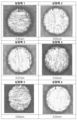
- Figure 1 is a microscope photograph measuring the width of the residue after development in Experimental Example 1-6.
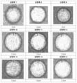
- Figure 2 is a microscope photograph measuring the width of the residue after development in Experimental Example 7-15.
- the present invention provides excellent developability and resolution by controlling the length of the residue after development of a resin composition for solder resist, and at the same time, stable reliability can be provided to a semiconductor substrate because no cured film residue remains on the substrate after alkali development.
- Developability refers to a property in which a portion that has not been cured by light is cleanly removed without residue in the development process
- resolution refers to a property in which a predetermined circuit pattern is precisely implemented.
- the resin composition for solder resist according to the present invention has excellent developability as the width of the residue after development is 1 ⁇ m or less, for example, 0.7 ⁇ m or less, or as another example, less than 0.5 ⁇ m. If the width of the residue after development exceeds the above-mentioned range, the amount of the film residue remaining on the substrate after alkaline development is large, so that not only is it difficult to form a circuit of a semiconductor package in a desired pattern, but also defects in the semiconductor package may be caused, thereby reducing reliability. In particular, if the amount of the film residue remaining on the substrate increases and the width of the residue increases, not only is it difficult to form a fine circuit pattern in a desired shape, but also when mounting a semiconductor device on the substrate, smooth current supply may not be possible.
- the width of the residue can be measured by the following method.
- the resin composition for solder resist is applied onto a substrate, exposed using a circular exposure film having a diameter of 100 ⁇ m, and the width of the residue is measured under an electron microscope after alkaline development.
- the portion exposed to light during exposure is cured, and the portion on which the circular exposure film is placed is not exposed to light and is therefore uncured. If the uncured portion is completely removed during alkaline development, a circular pattern having the same size as the exposure film is formed. However, if the developability is reduced and the pattern is not completely removed, a circular pattern having a diameter smaller than the exposure film is formed and a residue is formed as a band around the peripheral edge thereof.
- the present invention provides a resin composition for solder resist having excellent developability by controlling the width of the residue to 1 ⁇ m or less.
- the resin composition for solder resist according to the present invention comprises a carboxylic acid-containing photosensitive resin, an epoxy resin, an epoxy group-free phenolic resin, and a photoinitiator.
- the resin composition for solder resist according to the present invention may further comprise additives commonly used in the relevant technical field to impart various functions, such as a hydrophobic oligomer, an acrylic monomer, a solvent, a pigment, a catalyst, an ion catcher, a dispersant, a filler, etc., within the range that does not impair the purpose and effect of the present invention.
- the functional group such as “acid value” used in this specification is measured by a conventional method known in the art, and can be measured, for example, by a titration method.
- the “weight average molecular weight” is measured by a conventional method known in the art, and can be measured, for example, by a gel permeation chromatography (GPC) method.
- the “softening point” is measured by a conventional method known in the art, and can be measured, for example, by a dropping point meter (Dropping Point system calorimetry DP70) of Mettler Toledo.
- the photosensitive resin serves to impart photocurability and developability to the photosensitive resin composition.
- the resin composition for solder resist of the present invention includes a carboxylic acid-containing photosensitive resin as the photosensitive resin.
- the above carboxylic acid-containing photosensitive resin may be an acid-modified acrylate.
- the acid-modified acrylate may be produced by copolymerizing an ethylenically unsaturated compound monomer containing an acid functional group and an ethylenically unsaturated compound monomer copolymerizable with the above monomer.
- (meth)acrylic acid, itaconic acid, maleic acid, maleic anhydride, fumaric acid, and maleic acid alkyl esters can be used, and these can be used alone or in combination of two or more.
- maleic acid alkyl esters examples include, but are not limited to, monomethyl maleic acid, ethyl maleic acid, n-propyl maleic acid, isopropyl maleic acid, n-butyl maleic acid, n-hexyl maleic acid, n-octyl maleic acid, 2-ethylhexyl maleic acid, n-nonyl maleic acid, n-dodecyl maleic acid, and the like.
- Non-limiting examples of ethylenically unsaturated compound monomers copolymerizable with the ethylenically unsaturated compound monomer containing the above acid group include (meth)acrylic acid esters, styrene, styrene derivatives, and the like.
- the acid-modified acrylate may be one represented by the following chemical formula 1.
- n is an integer between 5 and 50
- n is an integer between 5 and 50.
- the carboxylic acid-containing photosensitive resin of the present invention may be any of the photosensitive resins (A-1) to (A-5) below, and these may be used alone or in combination of two or more thereof.
- a photosensitive resin containing a carboxyl group obtained by reacting a compound having two or more phenolic hydroxyl groups in one molecule with an alkylene oxide, reacting the reaction product obtained with an unsaturated group-containing monocarboxylic acid, and reacting the reaction product obtained with a polybasic acid anhydride.
- a photosensitive resin containing a carboxyl group which is obtained by reacting a compound having two or more phenolic hydroxyl groups in one molecule with a cyclic carbonate compound, reacting the reaction product obtained with an unsaturated group-containing monocarboxylic acid, and reacting the reaction product obtained with a polybasic acid anhydride.
- a photosensitive resin containing a carboxyl group obtained by reacting an alkylene oxide or an alkylene cyclic carbonate with a phenolic or novolac resin having two or more phenolic hydroxyl groups per molecule, reacting an acrylic or methacrylic monomer having an isocyanate group with the product obtained by reacting the phenolic or novolac resin having two or more phenolic hydroxyl groups per molecule, and then reacting the remaining hydroxyl groups with an acid anhydride.
- the above carboxylic acid-containing photosensitive resin may be used having an acid value of 30 to 200 mgKOH/g, for example, 50 to 100 mgKOH/g. If the acid value is below the above-mentioned range, the developability for alkaline water may be reduced and residues may be left on the substrate, and if it exceeds the above-mentioned range, detachment of the pattern may occur.
- the above carboxylic acid-containing photosensitive resin may be used having a weight average molecular weight of 3,000 to 30,000 g/mol, for example, 10,000 to 20,000 g/mol. If the weight average molecular weight is less than the above-mentioned range, the binding function between the components required as a binder resin is weak, and the resin may not be able to withstand physical external force during development, which may cause the pattern to be lost, or the heat resistance, solvent resistance, etc. may be poor. On the other hand, if the weight average molecular weight exceeds the above-mentioned range, the developability for an alkaline developer may be poor, and the flowability may deteriorate, making it difficult to control the thickness of the coating film or secure uniformity.
- the photosensitive resin composition of the present invention may contain 25 to 55 parts by weight, for example, 30 to 50 parts by weight, of the carboxylic acid-containing photosensitive resin. If the content of the carboxylic acid-containing photosensitive resin is less than the above-mentioned range, physical properties such as heat resistance and solvent resistance may deteriorate, and if it exceeds the above-mentioned range, storage stability may deteriorate and flowability may deteriorate, thereby deteriorating workability.
- the resin composition for solder resist according to the present invention comprises an epoxy resin.
- the epoxy resin imparts thermosetting properties to the photosensitive resin composition, and can form a solder resist layer by thermosetting the pattern remaining after exposure and development.
- polyglycidyl ethers of polyhydric phenols and derivatives thereof can be used.
- polyglycidyl ethers of polyhydric phenols such as bisphenol A type epoxy resin, hydrogenated bisphenol A type epoxy resin, bisphenol F type epoxy resin, novolac epoxy resin, phenol-novolac epoxy resin, cresol-novolac epoxy resin, N-glycidyl epoxy resin, bisphenol A type novolac epoxy resin, chelate epoxy resin, glyoxane epoxy resin, amino group-containing epoxy resin, rubber-modified epoxy resin, dicyclopentadiene phenolic epoxy resin, silicon-modified epoxy resin, ⁇ -caprolactone-modified epoxy resin, bisphenol S epoxy resin, diglycidyl phthalate resin, heterocyclic epoxy resin, and biphenyl epoxy resin can be used.
- the above epoxy resin may be used by mixing two or more types of epoxy resins.
- the epoxy resin may include a bisphenol-type epoxy resin and a biphenyl epoxy resin.
- the epoxy resin may include a bisphenol A-type epoxy resin and a biphenyl epoxy resin.
- the bisphenol A type epoxy resin may be one having an epoxy equivalent of 200 to 600 g/eq, for example, 400 to 550 g/eq, a softening point of 50 to 100° C., and a weight average molecular weight of 1,000 to 5,000 g/mol, for example, 1,000 to 3,000 g/mol.
- the bisphenol-type epoxy resin may be a bisphenol A-type epoxy resin represented by the following chemical formula 4.
- the biphenyl epoxy resin may be one having an epoxy equivalent of 100 to 1,000 g/eq, for example, 100 to 300 g/eq, a softening point of 50 to 150°C, and a weight average molecular weight of 300 to 10,000 g/mol, for example, 300 to 1,000 g/mol.
- an epoxy equivalent of 100 to 1,000 g/eq for example, 100 to 300 g/eq
- a softening point of 50 to 150°C a weight average molecular weight of 300 to 10,000 g/mol, for example, 300 to 1,000 g/mol.
- the biphenyl epoxy resin may be represented by the following chemical formula 5.
- R is an alkyl group having 1 to 5 carbon atoms.
- the above epoxy resin may further include an aliphatic epoxy resin, a fatty acid epoxy resin derived from a natural product, a polybutadiene epoxy resin, a cycloaliphatic epoxy resin, etc. These may be used alone or in a mixture of two or more types.
- the resin composition for solder resist of the present invention may contain 3 to 30 parts by weight, for example, 10 to 30 parts by weight, of the epoxy resin.
- it may contain 1.5 to 15 parts by weight, for example, 5 to 15 parts by weight, of the bisphenol A type epoxy resin and 1.5 to 15 parts by weight, for example, 5 to 15 parts by weight, of the biphenyl epoxy resin.
- the resin composition for solder resist of the present invention comprises a phenol-based resin that does not contain an epoxy group.
- a solder resist is manufactured by applying a photocurable composition on a substrate, placing an exposure film having a circuit pattern formed thereon, and exposing it to light. The portion exposed to light during exposure is cured, and the portion where the exposure film is placed and not exposed to light is uncured. Thereafter, the uncured portion is removed with a developer, so that a solder resist layer having a desired circuit pattern can be formed on the substrate. If the portion not exposed to light during development is cleanly removed by the developer, the circuit board conducts electricity smoothly, so that a highly reliable PCB substrate can be manufactured.
- the unexposed portion is affected by the light, so that it is not cleanly removed by the developer, and residues remain, resulting in a problem of reduced reliability.
- the epoxy-group-free phenol-based resin has no unsaturated group and epoxy group in its molecule, thereby preventing oxidation, suppressing radical reactions at an uncured interface that is not exposed to light and is not cured, and having acid properties, so that an uncured film can be easily removed by an alkaline developer during development.
- the developing time for removing an uncured portion can be shortened, and the width of the residue left in the cured film can be minimized, thereby significantly improving the resolution and reliability of a solder resist film manufactured using the same.
- the resin composition for solder resist of the present invention can suppress a reaction due to heat during a storage process, thereby improving the storability.
- the above epoxy group-free phenolic resin may include a phenol novolac resin, a cresol novolac resin, or a mixture thereof.
- the acid value of the epoxy-free phenol-based resin may be 80 to 150 g/eq, for example, 100 to 130 g/eq.
- the acid value of the epoxy-free phenol-based resin is less than 80 g/eq, developability by an alkaline developer may deteriorate, and when it exceeds 150 g/eq, hydrophilicity may increase, which may cause surface quality to deteriorate during alkaline development.
- the weight average molecular weight of the epoxy-free phenol-based resin may be 800 to 5,000 g/mol, for example, 1,000 to 4,000 g/mol.
- the weight average molecular weight of the epoxy-free phenol-based resin is less than 800 g/mol, a sufficient network may not be formed during a curing reaction with epoxy, which may deteriorate reliability, and when it exceeds 5,000 g/mol, alkaline developability may deteriorate.
- the above phenol novolac resin can be represented by the following chemical formula 2.
- cresol novolac phenol resin can be represented by the following chemical formula 3.
- the resin composition for solder resist of the present invention may contain 1 to 7 parts by weight, for example, 2 to 6 parts by weight, of the epoxy group-free phenolic resin. If the content of the epoxy group-free phenolic resin is less than 1 part by weight, the acidity may decrease, the photocuring reaction may not be controlled, and thus the developability may decrease and residue may remain. If it exceeds 7 wt%, deterioration due to acidity may occur during alkaline development.
- the resin composition for solder resist of the present invention contains a photoinitiator.
- the photoinitiator improves the curability of the photosensitive resin composition, thereby improving not only surface but also deep curability, thereby improving the ability to form a fine pattern.
- the photoinitiator may include a benzophenone-based compound, a benzoin alkyl ether-based compound, an acetophenone-based compound, a thioxanthone-based compound, an alkylanthraquinone-based compound, and an acylphosphine oxide-based compound.
- the photoinitiator may be an ⁇ -amino acetophenone-based compound, for example, 2-benzyl-2-dimethylamino-1-(4-morpholino-phenyl)-1-butanone, 2-methyl-1-[(4-methylthio)phenyl]-2-(4-morpholino-phenyl)-1-propanol, 2-(4-methylbenzyl)-2-(dimethylamino)-1-(4-morpholinophenyl)butan-1-one, and the like. These may be used alone or in combination of two or more.
- the resin composition for solder resist of the present invention may contain 1 to 15 parts by weight of the photoinitiator, for example, 1 to 5 parts by weight. If the content of the photoinitiator is less than the above-mentioned range, the radical initiation reaction does not occur smoothly upon exposure to light, making it difficult for curing to proceed, which may inhibit film formation and pattern formation, and if it exceeds the above-mentioned range, the reaction speed between the radical of the photoinitiator and the double bond may be too fast, making it difficult for the curing reaction to proceed uniformly on the surface or deep, or making it difficult to form a high molecular weight, which may make it difficult to form a film.
- the resin composition for solder resist according to the present invention may further contain an acrylic monomer.
- the acrylic monomer serves to impart photocurability.
- the above acrylic monomer may be a multifunctional acrylic monomer, for example, a (meth)acrylate monomer having three or more functions, or another example, three to six functions. In this case, sufficient photocurability may be imparted. If the functional group of the acrylic monomer is less than three functional groups, photocuring may not occur sufficiently, and thus deep curability may be reduced or HAST (Highly accelerated stress tester) resistance may be reduced.
- HAST Highly accelerated stress tester
- Non-limiting examples of the above multifunctional acrylic monomers include trifunctional (meth)acrylate monomers such as trimethylolpropane tri(meth)acrylate, pentaerythritol tri(meth)acrylate, etc.; tetrafunctional (meth)acrylate monomers such as pentaerythritol tetra(meth)acrylate, ditrimethylolpropane tetra(meth)acrylate, etc.; dipentaerythritol poly(meth)acrylates such as dipentaerythritol hexa(meth)acrylate, etc., which may be used alone or in a mixture of two or more.
- the resin composition for solder resist of the present invention may contain 1 to 20 parts by weight, for example, 1 to 10 parts by weight, of the acrylic monomer. If the content of the acrylic monomer is less than the above-mentioned range, the photocurability may be insufficient, making it difficult to form a pattern by alkaline development after light irradiation, and if it exceeds the above-mentioned range, the touch-drying property of the coating film may be reduced, or the solubility of the resin composition in an alkaline aqueous solution, which is a developer, may be reduced, making the coating film vulnerable.
- the resin composition for solder resist according to the present invention may further contain an organic solvent, a hydrophobic oligomer, a pigment, a filler, and other additives as needed.
- Organic solvents are used for viscosity adjustment and are not particularly limited as long as they are used in the relevant technical field.
- dipropylene glycol monoethyl ether, naphtha, etc. can be used.
- Pigments are used to impart a coloring effect, and are not particularly limited as long as they are used in the relevant technical field.
- azo pigments phthalocyanine pigments, etc. can be used.
- the filler is intended to improve properties such as strength, and is not particularly limited as long as it is used in the relevant technical field.
- inorganic fillers such as barium sulfate, talc, silica, aluminum oxide, and aluminum hydroxide can be used.
- barium sulfate having a particle size (D 50 ) of 20 ⁇ m or less, for example, 10 ⁇ m or less, and as another example, 1 ⁇ m or less can be used.
- the resin composition for solder resist of the present invention may contain 10 to 40 parts by weight of the filler, for example, 20 to 30 parts by weight.
- the strength of the coating film may be lowered, or the viscosity of the composition may increase, which may lower the smoothness of the coating film and make it difficult for light to reach the deep portion, thereby lowering the deep curability, which may cause an undercut phenomenon.
- Hydrophobic oligomers can impart photocurability and reduce heat stress.
- a non-limiting example of the hydrophobic oligomer is an epoxidized polybutadiene resin.
- the resin composition for solder resist of the present invention may contain 1 to 20 parts by weight of the hydrophobic oligomer, for example, 1 to 10 parts by weight. If the content of the hydrophobic oligomer exceeds the above-mentioned range, the curability may be reduced, causing an undercut phenomenon, or cracks may occur in the formed coating film due to heat stress.
- additives commonly used in the relevant technical field such as catalysts and ion catchers
- the catalyst is intended to promote the thermosetting reaction, and is not particularly limited as long as it is used in the relevant technical field.
- melamine, etc. can be used.
- the ion catcher is intended to remove the eluted ions, and is not particularly limited as long as it is used in the relevant technical field.
- Al, Mg, Zr series inorganic materials, etc. can be used.
- it may include finely divided silica that imparts thixotropic properties, a dispersant that helps disperse the filler, and an antifoaming agent for forming a smooth coating surface.
- each component was mixed to prepare a resin composition for each experimental example.
- the resin composition for each experimental example was applied to a copper substrate by screen printing, dried in a hot air oven at 80°C for 40 minutes, and then cooled to room temperature. If the drying time exceeds 50 minutes, the resolution may be reduced due to thermal curing.
- An exposure film patterned according to the original size was pressed onto each substrate, exposed at 900 mJ/cm2 through an exposure device equipped with a high-pressure mercury lamp, developed for 120 seconds in a 1% sodium carbonate aqueous solution at 30°C, and rinsed with DI water for 1 minute to form a pattern.
- the opening size was measured with a microscope (VHX-600ESO, Keyence, 700x magnification) based on a size of 100 ⁇ m, and the maximum width among the areas that appeared in the shape of a brass-colored ring, not a copper-colored one, was measured to evaluate the width of the residue after development.
- the width of the residue of each experimental example is shown in Tables 1 and 2 and Figures 1 and 2.
- Photosensitive resin Acid-modified acrylate (cresol novolac phenol modified, acid value 90 mgKOH/g, Mw 12,000)
- Phthalic acid monomer acid value 271 g/eq, Mw 304
- Cresol novolac epoxy resin acid value 210 g/eq, Mw 580
- Novolac epoxy resin acid value 180 g/eq, Mw 580
- Epoxy resin 1 Bisphenol A type epoxy resin (Cas no. 25068-38-6, EEW 450-500 g/eq, Mw 2,000)
- Epoxy resin 2 Biphenyl epoxy resin (Cas no. 89118-70-7, EEW 180 g/eq, Mw 354)
- Hydrophobic oligomer Epoxidized polybutadiene resin (Cas no. 71342-74-0, EEW 193 g/eq, Viscosity(45 °C) 29,000 mPa.s)
- Acrylic monomer DPHA (Dipentaerythritol hexa acrylate)
- Photoinitiator 2-Benzyl-2-dimethylamino-1-(4-morpholino-phenyl)-1-butanone
- Ion catcher A mixture of Mg 6 Al 2 [(OH) 16 CO 3 ]*4H 2 O 70% and Zr(HPO 4 ) 2 30%
- Pigment 1 Azo pigment
- Pigment 2 Phthalocyanine pigment
- Solvent 1 Dipropylene glycol monomethyl ether
- the resin composition of each experimental example was applied to a substrate by screen printing, dried at 80°C for 40 minutes, and cooled to room temperature. Afterwards, the resin composition was developed with a 1% sodium carbonate aqueous solution at 30°C, and the time until no residue remained (developing time) was measured.
- the resin composition of each experimental example was applied onto a substrate by screen printing, dried at 80°C for 40 minutes, and cooled to room temperature.
- a circular exposure film (diameter 100 ⁇ m) having a pattern formed thereon was placed and pressed, exposed at 900 mJ/cm2 through an exposure device equipped with a high-pressure mercury lamp, developed in a 1% sodium carbonate aqueous solution at 30°C for 120 seconds, rinsed with DI water for 1 minute, and heat-cured in a hot air oven (150°C) for 1 hour.
- the 100 ⁇ m-sized opening area of the substrate manufactured in this way was observed using a microscope (VHX-600ESO, Keyenece, x 700 magnification), and the minimum opening size that maintained a circular shape was measured to evaluate the resolution.
- the resin compositions of Experimental Examples 1-6 according to the present invention in which the width of the residue was 1 ⁇ m or less, exhibited excellent developability with a short developing time, and at the same time, exhibited high resolution with a minimum opening size of 80 ⁇ m or more.
- the resin compositions of Experimental Examples 7-15 in which the width of the residue after developing exceeded 1 ⁇ m, exhibited properties that were inferior to those of Experimental Examples 1-6 in all measured items.
- the present invention provides a resin composition for solder resist which provides excellent developability, resolution, and reliability.
- the resin composition for solder resist of the present invention provides excellent developability and resolution with a width of residue after development of 1 ⁇ m or less, and at the same time, no cured film residue remains on the substrate after development, so that stable reliability can be provided to the semiconductor substrate.
Landscapes
- Chemical & Material Sciences (AREA)
- Health & Medical Sciences (AREA)
- Chemical Kinetics & Catalysis (AREA)
- Medicinal Chemistry (AREA)
- Polymers & Plastics (AREA)
- Organic Chemistry (AREA)
- Engineering & Computer Science (AREA)
- Manufacturing & Machinery (AREA)
- Microelectronics & Electronic Packaging (AREA)
- Non-Metallic Protective Coatings For Printed Circuits (AREA)
Abstract
본 발명은 우수한 현상성, 해상성 및 신뢰성을 제공하는 솔더 레지스트용 수지 조성물에 관한 것이다.
Description
본 발명은 우수한 현상성, 해상성 및 신뢰성을 제공하는 솔더 레지스트용 수지 조성물에 관한 것이다.
감광성 수지 조성물은 포토 리소그래피의 원리를 응용하여 다양한 형태의 미세 패턴을 형성할 수 있기 때문에, 전자 기기나 인쇄 회로 기판 상에 미세 회로 패턴을 형성하는데 다양한 형태로 활용되고 있다. 예를 들어, 인쇄 배선 기판 제조, 액정 표시판 제조 또는 인쇄 제판 등에 감광성 수지 조성물이 이용되고 있다.
솔더 레지스트(Solder Resist)는 인쇄 회로 기판 보호재로서 솔더 형성 시 솔더가 불필요한 부위에 부착되는 것을 막고 솔더 브리지가 형성되지 않도록 하는 동시에, 도전부의 전기 절연성을 유지하는 목적으로 사용된다. 기판의 초대형화 및 박막화에 따라, 얇은 두께의 코팅층을 폭넓게 형성할 수 있고 높은 정밀도를 갖는 솔더 레지스트에 대한 다양한 연구가 진행되고 있다. 일례로, 특허 제10-1063048호는 카르복실기 함유 감광성 수지, 옥심 에스테르계 광중합 개시제, 에틸렌성 불포화기를 갖는 화합물 및 열경화성 성분을 포함하는 알칼리 현상형 솔더 레지스트를 개시하고 있다.
최근, 전자 기기의 소형화와 경량화에 따라, 패키지 및 인쇄 배선판의 고집적, 고밀도화가 가속화되면서 미세 회로 패턴에 대한 요구가 증가하고, 그에 따라 더 얇은 두께에서 높은 정밀도를 나타내는 고해상도 솔더 레지스트에 대한 수요가 높아지고 있다. 분자 내 이중결합 및 카르복실산기를 두개 이상 가지고 있고, 분자량이 비교적 높은 감광성 수지를 주 수지로 사용하는 종래의 솔더 레지스트의 경우, 도막의 경도를 향상시키고 공정상 발생 가능한 외관 불량을 개선할 수 있다는 점에서 효과적이나, 알칼리 현상액에 완전히 제거되지 못하여 현상성이 저하되고, 높은 해상도를 제공하지 못하는 문제가 있다. 또한, 알칼리 현상 후 기판에 미경화된 조성물의 잔여물이 남아, 반도체 패키지의 해상도, 절연 특성 및 신뢰성이 저하되는 문제가 있었다.
이에, 우수한 현상성, 해상성 및 신뢰성을 제공할 수 있는, 솔더 레지스트용 수지 조성물이 요구된다.
본 발명은 우수한 현상성, 해상성 및 신뢰성을 제공하는 솔더 레지스트용 수지 조성물을 제공한다.
본 발명은 카르복실산 함유 감광성 수지, 에폭시 수지, 에폭시기 미함유 페놀계 수지 및 광개시제를 포함하고, 현상 후 잔여물(residue)의 폭이 1 ㎛ 이하인 솔더 레지스트용 수지 조성물을 제공한다.
본 발명은 우수한 현상성, 해상성 및 신뢰성을 제공하는 솔더 레지스트용 수지 조성물을 제공한다. 본 발명의 솔더 레지스트용 수지 조성물은 현상 후 잔여물의 폭이 1 ㎛ 이하로, 우수한 현상성 및 해상성을 제공하는 동시에, 현상 후 기판에 경화 도막 잔여물이 남지 않아 반도체 기판에 안정적인 신뢰성을 제공할 수 있다.
도 1은 실험예 1-6의 현상 후 잔여물의 폭을 측정한 현미경 사진이다.
도 2는 실험예 7-15의 현상 후 잔여물의 폭을 측정한 현미경 사진이다.
이하, 본 발명에 대하여 상세히 설명한다. 그러나, 하기 내용에 의해서만 한정되는 것은 아니며, 필요에 따라 각 구성요소가 다양하게 변형되거나 선택적으로 혼용될 수 있다. 따라서, 본 발명의 사상 및 기술 범위에 포함되는 모든 변경, 균등물 내지 대체물을 포함하는 것으로 이해되어야 한다.
본 발명은 솔더 레지스트용 수지 조성물의 현상 후 잔여물의 길이를 제어함으로써, 우수한 현상성 및 해상성을 제공하는 동시에, 알칼리 현상 후 기판에 경화 도막 잔여물이 남지 않아 반도체 기판에 안정적인 신뢰성을 제공할 수 있다. 현상성은 광에 의해 경화되지 않은 부분이 현상 공정에서 잔여물 없이 깨끗하게 제거되는 성질을 의미하고, 해상성은 소정의 회로 패턴을 정밀하게 구현하는 성질을 의미한다.
본 발명에 따른 솔더 레지스트용 수지 조성물은 현상 후 잔여물(residue)의 폭이 1 ㎛ 이하, 예를 들어 0.7 ㎛ 이하, 다른 예로 0.5 ㎛ 미만으로 현상성이 우수하다. 현상 후 잔여물의 폭이 전술한 범위를 초과하는 경우, 알칼리 현상 후 기판에 잔류하는 도막 잔여물의 양이 많아, 반도체 패키지의 회로를 원하는 패턴으로 형성하기 어려울 뿐만 아니라, 반도체 패키지의 불량을 초래하여 신뢰성을 저하시킬 수 있다. 특히, 기판 상 잔류하는 도막 잔여물의 양이 증가하고, 잔여물의 폭이 증가되면, 원하는 형태의 미세한 회로 패턴을 형성하기 어려울 뿐만 아니라, 기판 상에 반도체 소자 실장 시, 원활한 전류 공급을 하지 못할 수 있다.
상기 잔여물의 폭은 하기 방법으로 측정할 수 있다. 상기 솔더 레지스트용 수지 조성물을 기판 상에 도포하고, 지름이 100 ㎛인 원 형태의 노광 필름을 사용하여 노광하고, 알칼리 현상 후 전자 현미경으로 잔여물의 폭을 측정한다. 노광 시 광에 노출되는 부분은 경화되고, 원 형태의 노광 필름이 놓여진 부분은 광에 노출되지 않아 미경화된다. 알칼리 현상 시 미경화된 부분이 완전하게 제거되면 노광 필름 크기와 동일한 크기로 원형 패턴이 형성되나, 현상성이 저하되어 완전히 제거되지 않는 경우 노광 필름 보다 작은 지름의 원형 패턴이 형성되고 그 주변 가장자리에 잔여물(residue)이 띠를 두른 것처럼 형성된다. 본 발명은 이러한 잔여물의 폭을 1 ㎛ 이하로 제어함으로써, 현상성이 우수한 솔더 레지스트용 수지 조성물을 제공한다.
본 발명에 따른 솔더 레지스트용 수지 조성물은 카르복실산 함유 감광성 수지, 에폭시 수지, 에폭시기 미함유 페놀계 수지 및 광개시제를 포함한다. 본 발명에 따른 솔더 레지스트용 수지 조성물은 소수성 올리고머, 아크릴 모노머, 용제, 안료, 촉매, 이온 캐처, 분산제, 충진재 등, 본 발명의 목적과 효과를 저해하지 않는 한도 내에서 다양한 기능을 부여하기 위해 해당 기술분야에서 통상적으로 사용되는 첨가제를 더 포함할 수 있다.
본 명세서에서 사용된 “산가”와 같은 작용기가는 해당 기술분야에 알려진 통상의 방법에 의해 측정된 것이며, 예를 들어 적정(titration)의 방법으로 측정할 수 있다. “중량평균분자량"은 해당 기술분야에 알려진 통상의 방법에 의해 측정된 것이며, 예를 들어 GPC(gel permeation chromatograph) 방법으로 측정할 수 있다. “연화점”은 해당 기술분야에 알려진 통상의 방법에 의해 측정된 것이며, 예를 들어 메틀러 토레도(Mettler Toledo)社의 적점 측정기(Dropping Point system calorimetry DP70)로 측정할 수 있다.
카르복실산 함유 감광성 수지
감광성 수지는 감광성 수지 조성물에 광경화성 및 현상성을 부여하는 역할을 한다. 본 발명의 솔더 레지스트용 수지 조성물은 감광성 수지로 카르복실산 함유 감광성 수지를 포함한다.
상기 카르복실산 함유 감광성 수지는 산 변성 아크릴레이트일 수 있다. 일례로, 상기 산 변성 아크릴레이트는 산기(acid functional group)를 포함하는 에틸렌성 불포화 화합물 단량체 및 상기 단량체와 공중합 가능한 에틸렌성 불포화 화합물 단량체를 공중합하여 제조할 수 있다.
상기 산기를 포함하는 에틸렌성 불포화 화합물 단량체로는 (메타)아크릴산, 이타콘산, 말레인산, 무수말레인산, 푸마르산 및 말레인산 알킬 에스테르 등을 사용할 수 있고, 이들을 단독으로 또는 2종 이상 혼합하여 사용할 수 있다. 상기 말레인산 알킬 에스테르의 예로는 모노메틸 말레인산, 에틸 말레인산, n-프로필 말레인산, 이소프로필 말레인산, n-부틸 말레인산, n-헥실 말레인산, n-옥틸 말레인산, 2-에틸헥실 말레인산, n-노닐 말레인산, n-도데실 말레인산 등이 있으나, 이에 제한되는 것은 아니다.
상기 산기를 포함하는 에틸렌성 불포화 화합물 단량체와 공중합 가능한 에틸렌성 불포화 화합물 단량체의 비제한적인 예로는 (메타)아크릴산 에스테르, 스티렌, 스티렌 유도체 등을 들 수 있다. 예를 들어, 메틸 (메타)아크릴레이트, 에틸 (메타)아크릴레이트, 프로필 (메타)아크릴레이트, 부틸 (메타)아크릴레이트, 벤질 (메타)아크릴레이트, 디메틸아미노에틸 (메타)아크릴레이트, 이소부틸 (메타)아크릴레이트, t-부틸 (메타)아크릴레이트, 시클로헥실 (메타)아크릴레이트, 이소보닐 (메타)아크릴레이트, 에틸헥실 (메타)아크릴레이트, 2-페녹시에틸 (메타)아크릴레이트, 테트라하이드로퍼푸릴 (메타)아크릴레이트, 히드록시에틸 (메타)아크릴레이트, 2-히드록시프로필 (메타)아크릴레이트, 2-히드록시-3-클로로프로필 (메타)아크릴레이트, 4-히드록시부틸 (메타)아크릴레이트, 아실옥틸옥시-2-히드록시프로필 (메타)아크릴레이트, 글리세롤 (메타)아크릴레이트, 2-메톡시에틸 (메타)아크릴레이트, 3-메톡시부틸 (메타)아크릴레이트, 에톡시디에틸렌글리콜 (메타)아크릴레이트, 메톡시트리에틸렌글리콜 (메타)아크릴레이트, 메톡시트리프로필렌글리콜 (메타)아크릴레이트, 폴리(에틸렌글리콜)메틸에테르 (메타)아크릴레이트, 페녹시디에틸렌글리콜 (메타)아크릴레이트, p-노닐페녹시폴리프로필렌글리콜 (메타)아크릴레이트, 글리시딜 (메타)아크릴레이트, 테트라플루오로프로필 (메타)아크릴레이트, 헥사플루오로이소프로필 (메타)아크릴레이트옥타플루오로펜틸 (메타)아크릴레이트, 헵타데카플루오로데실 (메타)아크릴레이트, 트리브로모페닐 (메타)아크릴레이트, 메틸α-히드록시메틸 (메타)아크릴레이트, 에틸α-히드록시메틸 (메타)아크릴레이트, 프로필α-히드록시메틸 (메타)아크릴레이트, 부틸α-히드록시메틸 (메타)아크릴레이트, 디시클로펜타닐 (메타)아크릴레이트, 디시클로펜테닐 (메타)아크릴레이트, 디시클로펜타닐옥시에틸 (메타)아크릴레이트, 디시클로펜테닐옥시에틸 (메타)아크릴레이트와 같은 불포화 카르복실산 에스테르류; 스티렌, α-메틸스티렌, 비닐 톨루엔, 메톡시 스티렌, 클로로 스티렌과 같은 방향족 비닐류; 비닐 메틸 에테르, 비닐 에틸 에테르, 알릴 글리시딜 에테르와 같은 불포화 에테르류; N-비닐 피롤리돈, N-비닐 카바졸, N-비닐 모폴린과 같은 N-비닐 삼차아민류; N-페닐 말레이미드, N-(4-클로로페닐)말레이미드, N-(4-히드록시페닐)말레이미드, N-시클로헥실 말레이미드와 같은 불포화 이미드류; 무수 말레인산, 무수 메틸 말레인산과 같은 무수 말레인산류; 알릴 글리시딜 에테르, 글리시딜 (메타)아크릴레이트, 3,4-에폭시시클로헥실메틸 (메타)아크릴레이트와 같은 불포화 글리시딜 화합물류 또는 이들의 혼합물이 사용될 수 있으나 이에 제한되는 것은 아니다.
일례로, 상기 산변성 아크릴레이트로는 하기 화학식 1로 표시되는 것을 사용할 수 있다.
[화학식 1]

상기 화학식 1에서,
m은 5 내지 50의 정수이고,
n은 5 내지 50의 정수이다.
본 발명의 카르복실산 함유 감광성 수지는 하기 (A-1) 내지 (A-5)의 감광성 수지일 수 있으며, 이들을 단독으로 또는 2종 이상 혼합하여 사용할 수 있다.
(A-1) 불포화 카르복실산과 불포화기 함유 화합물의 공중합에 의해 얻어지는 카르복실기 함유 감광성 수지
(A-2) 2관능 고형 에폭시 수지의 수산기를 추가로 에피클로로히드린으로 에폭시화한 다관능 에폭시 수지에 (메트)아크릴산을 반응시키고, 생성된 수산기에 2염기산 무수물을 부가시킨 카르복실기 함유 감광성 수지
(A-3) 1분자 중에 2개 이상의 페놀성 수산기를 갖는 화합물과 알킬렌옥사이드를 반응시켜 얻어지는 반응 생성물에 불포화기 함유 모노카르복실산을 반응시키고, 얻어지는 반응 생성물에 다염기산 무수물을 반응시켜 얻어지는 카르복실기 함유 감광성 수지
(A-4) 1 분자 중에 2개 이상의 페놀성 수산기를 갖는 화합물과 환상 카보네이트 화합물을 반응시켜 얻어지는 반응 생성물에 불포화기 함유 모노카르복실산을 반응시키고, 얻어지는 반응 생성물에 다염기산 무수물을 반응시켜 얻어지는 카르복실기 함유 감광성 수지,
(A-5) 분자당 2개 이상의 페놀성 수산기를 갖는 페놀계 또는 노볼락계 수지에 알킬렌 옥사이드 또는 알킬렌 사이클릭 카보네이트를 반응시켜 얻은 생성물에 이소시아네이트기를 갖는 아크릴 또는 메타크릴 단량체를 반응시키고, 다시 남아있는 수산기에 산무수물을 반응시켜 얻어지는 카르복실기 함유 감광성 수지
상기 카르복실산 함유 감광성 수지로 산가가 30 내지 200 mgKOH/g, 예를 들어 50 내지 100 mgKOH/g인 것을 사용할 수 있다. 산가가 전술한 범위 미만인 경우 알칼리수에 대한 현상성이 낮아지고 기판에 잔사를 남길 수 있고, 전술한 범위를 초과하는 경우 패턴의 탈착이 일어날 수 있다.
상기 카르복실산 함유 감광성 수지로 중량평균분자량이 3,000 내지 30,000 g/mol, 예를 들어 10,000 내지 20,000 g/mol인 것을 사용할 수 있다. 중량평균분자량이 전술한 범위 미만인 경우 바인더 수지로서 요구되는 구성 성분 간 바인딩 기능이 약하고, 현상 시 물리적 외력에 견딜 수 없어 패턴이 소실되거나, 내열성, 내용제성 등이 열세해질 수 있다. 반면, 중량평균분자량이 전술한 범위를 초과하는 경우 알칼리 현상액에 대한 현상성이 열세해지고, 흐름성이 나빠져 코팅막 두께 제어나 균일성(uniformity) 확보가 어려워질 수 있다.
본 발명의 감광성 수지 조성물은 상기 카르복실산 함유 감광성 수지를 25 내지 55 중량부, 예를 들어 30 내지 50 중량부 포함할 수 있다. 카르복실산 함유 감광성 수지의 함량이 전술한 범위 미만인 경우 내열성, 내용제성 등의 물성이 저하될 수 있고, 전술한 범위를 초과하는 경우 저장 안정성이 저하되고, 흐름성이 나빠져 작업성이 저하될 수 있다.
에폭시 수지
본 발명에 따른 솔더 레지스트용 수지 조성물은 에폭시 수지를 포함한다. 에폭시 수지는 감광성 수지 조성물에 열경화성을 부여하여, 노광 및 현상 후 남은 패턴을 열경화시킴으로써 솔더 레지스트층을 형성할 수 있다.
상기 에폭시 수지로는 다가 페놀의 폴리글리시딜 에테르 및 그의 유도체 등을 사용할 수 있다. 예를 들어, 다가 페놀의 폴리글리시딜 에테르인 비스페놀 A형 에폭시 수지, 수소화 비스페놀 A형 에폭시 수지, 비스페놀 F형 에폭시 수지, 노볼락 에폭시 수지, 페놀-노볼락 에폭시 수지, 크레졸-노볼락 에폭시 수지, N-글리시딜 에폭시 수지, 비스페놀 A형 노볼락 에폭시 수지, 킬레이트형 에폭시 수지, 글리옥산 에폭시 수지, 아미노기 함유 에폭시 수지, 고무변성 에폭시 수지, 디시클로펜타디엔 페놀성 에폭시 수지, 규소 변성 에폭시 수지, ε- 카프로락톤 변성 에폭시 수지, 비스페놀 S 에폭시 수지, 디글리시딜 프탈레이트 수지, 헤테로 환상 에폭시 수지, 비페닐 에폭시 수지 등을 사용할 수 있다.
상기 에폭시 수지로 2종 이상의 에폭시 수지를 혼합하여 사용할 수 있다. 일례로, 상기 에폭시 수지는 비스페놀형 에폭시 수지 및 비페닐 에폭시 수지를 포함할 수 있다. 다른 예로, 상기 에폭시 수지는 비스페놀 A형 에폭시 수지 및 비페닐 에폭시 수지를 포함할 수 있다. 상기 2종의 에폭시 수지를 혼용하는 경우, 비스페놀형 에폭시 수지로부터 우수한 부착성 및 내화학성 효과를 얻는 동시에, 비페닐 에폭시 수지로부터 내열성 및 열건조 조건 하에서의 열안정성을 보완하는 효과를 얻을 수 있다.
상기 비스페놀 A형 에폭시 수지로는 에폭시 당량이 200 내지 600 g/eq, 예를 들어 400 내지 550 g/eq이고, 연화점이 50 내지 100 ℃이고, 중량평균분자량이 1,000 내지 5,000 g/mol, 예를 들어 1,000 내지 3,000 g/mol인 것을 사용할 수 있다. 비스페놀 A형 에폭시 수지의 물성이 전술한 범위를 만족하는 경우, 우수한 부착성 및 내화학성이 발현될 수 있다.
일례로, 상기 비스페놀형 에폭시 수지는 비스페놀 A형 에폭시 수지로, 하기 화학식 4로 표시되는 것일 수 있다.
[화학식 4]

상기 비페닐 에폭시 수지로는 에폭시 당량이 100 내지 1,000 g/eq, 예를 들어 100 내지 300 g/eq이고, 연화점이 50 내지 150 ℃이고, 중량평균분자량이 300 내지 10,000 g/mol, 예를 들어 300 내지 1,000 g/mol인 것을 사용할 수 있다. 비페닐 에폭시 수지의 물성이 전술한 범위를 만족하는 경우, 우수한 내열성 및 열안정성이 발현될 수 있다.
일례로, 상기 비페닐 에폭시 수지는 하기 화학식 5로 표시되는 것일 수 있다.
[화학식 5]

상기 화학식 5에서, R은 탄소수 1 내지 5개의 알킬기이다.
상기 에폭시 수지는 지방족계 에폭시 수지, 천연물에서 유래한 지방산계 에폭시 수지, 폴리부타디엔계 에폭시 수지, 사이클로지방족계 에폭시 수지 등을 더 포함할 수 있다. 이들은 단독으로 또는 2종 이상 혼합하여 사용될 수 있다.
본 발명의 솔더 레지스트용 수지 조성물은 상기 에폭시 수지를 3 내지 30 중량부, 예를 들어 10 내지 30 중량부 포함할 수 있다. 일례로, 상기 비스페놀 A형 에폭시 수지 1.5 내지 15 중량부, 예를 들어 5 내지 15 중량부 및 상기 비페닐 에폭시 수지 1.5 내지 15 중량부, 예를 들어 5 내지 15 중량부를 포함할 수 있다. 각 에폭시 수지의 함량이 전술한 범위 미만인 경우 경화 증진 효과가 불충분할 수 있고, 전술한 범위를 초과하는 경우 코팅 외관이 불량해지거나 코팅막의 강도가 약해질 수 있다.
에폭시기 미함유 페놀계 수지
본 발명의 솔더 레지스트용 수지 조성물은 에폭시기 미함유 페놀계 수지를 포함한다.
솔더 레지스트는 기판 상 광경화 조성물을 도포하고, 그 위에 회로 패턴이 형성된 노광 필름을 두고 광에 노출시켜 제조된다. 노광 시 광에 노출되는 부분은 경화되고, 노광 필름이 놓여져 광에 노출되지 않는 부분은 미경화된다. 이후, 미경화된 부분을 현상액으로 제거하여 기판 상에 원하는 회로 패턴을 가진 솔더 레지스트층을 형성할 수 있다. 현상 시 광에 노출되지 않는 부분이 현상액에 의해 깨끗하게 제거되는 경우 회로 기판의 통전이 원활하게 되어 신뢰성이 높은 PCB 기판을 제조할 수 있다. 반면, 광에 노출되는 부분(노출부)과 노출되지 않는 부분(미노출부)이 맞닿는 경계면에서 미노출부가 광에 의해 영향을 받아 현상액에 의해 깨끗하게 제거되지 않고 잔사가 남아 잔여물이 발생되고, 그 결과 신뢰성이 저하되는 문제가 발생될 수 있다.
특히, 솔더 레지스트층을 형성하는 조성물 내 에폭시기 함유 페놀계 수지 또는 에폭시 화합물로부터 유래되는 페놀계 수지가 포함되면, 솔더 레지스트 제조 공정 중 노광에 의해 광경화되는 노출부의 영향을 받아 미노출부에서도 라디칼 반응이 발생됨에 따라 경화가 발생되어 현상성이 저하되는 문제가 있었다.
본 발명에서는 에폭시기 미함유 페놀계 수지를 적용함으로써, 이러한 잔여물의 발생을 최소화시킬 수 있다. 구체적으로, 상기 에폭시기 미함유 페놀계 수지는 분자 내 불포화기 및 에폭시기가 없어 산화를 방지하고, 광에 노출되지 않아 경화되지 않는 미경화 계면에서 라디칼 반응을 억제하고, 산(acid) 특성을 가지고 있어 현상 시 미경화 도막이 알칼리 현상액에 의해 쉽게 제거될 수 있다. 이로 인해 경화되지 않은 부분을 제거하는 현상 시간을 단축하고 경화 도막에 남겨진 잔여물의 폭을 최소화시켜, 이를 사용하여 제조된 솔더 레지스트 도막의 해상성 및 신뢰성을 현저히 향상시킬 수 있다. 또한, 본 발명의 솔더 레지스트용 수지 조성물의 저장 과정 중 열에 의한 반응을 억제하여 저장성을 향상시킬 수 있다.
상기 에폭시기 미함유 페놀계 수지는 페놀 노볼락 수지, 크레졸 노볼락 수지 또는 이들의 혼합물을 포함할 수 있다.
상기 에폭시기 미함유 페놀계 수지의 산가는 80 내지 150 g/eq, 예를 들어 100 내지 130 g/eq일 수 있다. 에폭시기 미함유 페놀계 수지의 산가가 80 g/eq 미만인 경우 알칼리 현상액에 의한 현상성이 저하될 수 있고, 150 g/eq를 초과하는 경우 친수도가 증가하여 알칼리 현상 시 표면 품질 저하가 초래될 수 있다. 상기 에폭시기 미함유 페놀계 수지의 중량평균분자량은 800 내지 5,000 g/mol, 예를 들어 1,000 내지 4,000 g/mol일 수 있다. 에폭시기 미함유 페놀계 수지의 중량평균분자량이 800 g/mol 미만인 경우 에폭시와 경화 반응 시 충분한 네트워크를 형성하지 못하여 신뢰성이 저하될 수 있고, 5,000 g/mol를 초과하는 경우 알칼리 현상성이 저하될 수 있다.
상기 페놀 노볼락 수지는 하기 화학식 2로 표시될 수 있다.
[화학식 2]

상기 크레졸 노볼락 페놀 수지는 하기 화학식 3으로 표시될 수 있다.
[화학식 3]

본 발명의 솔더 레지스트용 수지 조성물은 상기 에폭시기 미함유 페놀계 수지를 1 내지 7 중량부, 예를 들어 2 내지 6 중량부 포함할 수 있다. 에폭시기 미함유 페놀계 수지의 함량이 1 중량부 미만인 경우 산도가 저하되고, 광경화 반응을 조절하지 못해 현상성이 저하되어 잔사가 남을 수 있고, 7 중량%를 초과하는 경우 알칼리 현상 시 산도에 의한 열화가 발생할 수 있다.
광개시제
본 발명의 솔더 레지스트용 수지 조성물은 광개시제를 포함한다. 광개시제는 감광성 수지 조성물의 경화성을 향상시켜, 표면뿐만 아니라 심부 경화성을 향상시켜 미세 패턴 형성성을 향상시키는 역할을 한다.
상기 광개시제로는 벤조페논계 화합물, 벤조인알킬에테르계 화합물, 아세토페논계 화합물, 티옥산톤계 화합물, 알킬안트라퀴논계 화합물 및 아실포스핀옥시드계 화합물 등을 사용할 수 있다. 일례로, 상기 광개시제는 α-아미노 아세토페논계 화합물, 예를 들어 2-벤질-2-디메틸아미노-1-(4-모르폴리노-페닐)-1-부타논(2-Benzyl-2-dimethylamino-1-(4-morpholino-phenyl)-1-butanone), 2-메틸-1-[(4-메틸티오)페닐]-2-(4-모포리닐)-1-프로판올, 2-(4-메틸벤질)-2-(디메틸아미노)-1-(4-모포리노페닐)부탄-1-온 등일 수 있고, 이들을 단독으로 또는 2종 이상을 혼합하여 사용할 수 있다.
본 발명의 솔더 레지스트용 수지 조성물은 상기 광개시제를 1 내지 15 중량부, 예를 들어 1 내지 5 중량부 포함할 수 있다. 광개시제의 함량이 전술한 범위 미만인 경우 광 노출 시 라디칼 개시 반응이 원활히 일어나지 않아 경화가 진행되기 어려워 도막 형성 및 패턴 형성이 저해될 수 있고, 전술한 범위를 초과하는 경우 광개시제의 라디칼과 이중 결합과의 반응 속도가 너무 빨라 경화 반응이 표면 또는 심부에서 균일하게 진행되기 어려워지거나, 고분자량 형성이 어려워져 도막 형성이 어려워질 수 있다.
아크릴 모노머
본 발명에 따른 솔더 레지스트용 수지 조성물은 아크릴 모노머를 더 포함할 수 있다. 아크릴 모노머는 광경화성을 부여하는 역할을 한다.
상기 아크릴 모노머는 다관능 아크릴 모노머일 수 있고, 예를 들어 3관능 이상, 다른 예로 3 내지 6 관능의 (메타)아크릴레이트 모노머일 수 있다. 이 경우, 충분한 광경화성을 부여할 수 있다. 상기 아크릴 모노머의 관능기가 3관능기 미만일 경우 광경화가 충분히 일어나지 못해 심부 경화성이 저하되거나 HAST(Highly accelerated stress tester) 내성이 저하될 수 있다.
상기 다관능 아크릴 모노머의 비제한적인 예로는 트리메틸올프로판 트리(메타)아크릴레이트, 펜타에리트리톨 트리(메타)아크릴레이트 등과 같은 3관능 (메타)아크릴레이트 모노머; 펜타에리트리톨 테트라(메타)아크릴레이트, 디트리메틸올프로판 테트라(메타)아크릴레이트 등과 같은 4관능 (메타)아크릴레이트 모노머; 디펜타에리트리톨 헥사(메타)아크릴레이트와 같은 디펜타에리트리톨 폴리(메타)아크릴레이트 등이 있는데, 이들은 단독으로 사용되거나 2종 이상이 혼합되어 사용될 수 있다.
본 발명의 솔더 레지스트용 수지 조성물은 상기 아크릴 모노머를 1 내지 20 중량부, 예를 들어 1 내지 10 중량부 포함할 수 있다. 아크릴 모노머의 함량이 전술한 범위 미만인 경우 광경화성이 충분치 못하여 광조사 후 알칼리 현상에 의한 패턴 형성이 어려워질 수 있고, 전술한 범위를 초과하는 경우 도막의 지촉 건조성이 저하되거나, 현상액인 알칼리 수용액에 대한 수지 조성물의 용해성이 저하되어 도막이 취약해질 수 있다.
첨가제
본 발명에 따른 솔더 레지스트용 수지 조성물은 필요에 따라 유기 용제, 소수성 올리고머, 안료, 충진재 및 기타 첨가제를 더 포함할 수 있다.
유기 용제는 점도 조정을 위한 것으로, 해당 기술분야에 사용되는 것이라면 특별히 제한되지 않는다. 일례로, 디프로필렌글리콜 모노에틸 에테르, 나프타 등을 사용할 수 있다.
안료는 착색 효과를 부여하기 위한 것으로, 해당 기술분야에 사용되는 것이라면 특별히 제한되지 않는다. 일례로, 아조계 안료, 프탈로시아닌계 안료 등을 사용할 수 있다.
충진재는 강도 등의 물성 향상을 위한 것으로, 해당 기술분야에 사용되는 것이라면 특별히 제한되지 않는다. 일례로, 황산바륨, 탈크, 실리카, 산화알루미늄, 수산화알루미늄 등의 무기 필러가 사용될 수 있다. 이때, 입경(D50)이 20 ㎛ 이하, 예를 들어 10 ㎛ 이하, 다른 예로 1 ㎛ 이하인 황산바륨을 사용할 수 있다. 본 발명의 솔더 레지스트용 수지 조성물은 상기 충진재를 10 내지 40 중량부, 예를 들어 20 내지 30 중량부 포함할 수 있다. 상기 충진재의 함량이 전술한 범위를 벗어나게 되면 도막의 강도가 저하되거나 조성물의 점도 상승으로 인해 도막의 평활성이 낮아지고 광이 심부까지 닿기 어려워 심부 경화성이 저하되어 언더컷 현상이 발생될 수 있다.
소수성 올리고머는 광경화성을 부여하고, 열에 의한 스트레스를 감소 시킬 수 있다. 상기 소수성 올리고머의 비제한적인 예로는 에폭시화 폴리부타디엔 수지가 있다. 본 발명의 솔더 레지스트용 수지 조성물은 상기 소수성 올리고머를 1 내지 20 중량부, 예를 들어 1 내지 10 중량부 포함할 수 있다. 소수성 올리고머의 함량이 전술한 범위를 벗어나게 되면 경화성이 저하되어 언더컷 현상이 발생되거나, 열에 의한 스트레스로 인해 형성된 도막의 크랙이 발생될 수 있다.
이 외에, 촉매, 이온 캐처 등 해당 기술분야에서 통상적으로 사용되는 첨가제가 사용될 수 있다. 촉매는 열경화 반응을 촉진시키기 위한 것으로, 해당 기술분야에 사용되는 것이라면 특별히 제한되지 않는다. 일례로, 멜라민 등이 사용될 수 있다. 이온 캐처는 용출 이온을 제거하기 위한 것으로, 해당 기술분야에 사용되는 것이라면 특별히 제한되지 않는다. 일례로, Al, Mg, Zr 계열 무기물 등이 사용될 수 있다.
이 외에도, 요변성을 부여하는 미분 실리카, 필러의 분산을 돕는 분산제, 평활한 도막 표면을 형성하기 위한 소포제 등이 포함될 수 있다.
이하 실시예를 통하여 본 발명을 보다 구체적으로 설명한다. 그러나, 하기 실시예는 본 발명의 이해를 돕기 위한 것일 뿐, 어떠한 의미로든 본 발명의 범위가 실시예로 한정되는 것은 아니다.
[실험예 1-15]
하기 표 1, 2에 기재된 조성에 따라 각 성분을 혼합하여, 각 실험예의 수지 조성물을 제조하였다. 각 실험예의 수지 조성물을 구리 기판에 스크린 인쇄법으로 도포하고, 80 ℃에서 40 분 열풍 오븐으로 건조시킨 후, 실온으로 냉각하였다. 건조 시간이 50 분을 초과하면 열 경화에 의해 해상성이 저하될 수 있다. 각 기판에 원 사이즈 별로 패터닝 되어있는 노광 필름을 압착시키고, 고압 수은등이 탑재된 노광기를 통해 900 mJ/㎠로 노광한 후, 30 ℃, 1 % 탄산나트륨 수용액으로 120 초 동안 현상하고, DI water로 1 분 동안 수세하여 패턴을 형성하였다. 각 실험예의 수지 조성물이 형성한 여러 개의 원형 패턴 중 100 ㎛ 크기를 기준으로 오프닝 사이즈(opening size)를 현미경(VHX-600ESO, Keyence社, 700 배율)으로 측정하고, 구리 동색이 아닌 황동색의 고리 형태로 나타난 부위 중 최대 폭을 측정하여 현상 후 잔여물의 폭으로 평가하였다. 각 실험예의 잔여물의 폭은 표 1, 2 및 도 1, 2에 나타내었다.


감광성 수지: 산 변성 아크릴레이트(크레졸노볼락 페놀 변성, 산가 90 mgKOH/g, Mw 12,000)
페놀계 수지 1: 크레졸 노볼락 페놀 수지(산가 108 g/eq, Mw 1,500, 화학식 3의 화합물(n=13))
페놀계 수지 2: 페놀 노볼락 수지(산가 120 g/eq, Mw 3,500, 화학식 2의 화합물(n=23))
자일록 수지: 산가 320 g/eq, Mw 780
프탈산 모노머: 산가 271 g/eq, Mw 304
크레졸 노볼락 에폭시 수지: 산가 210 g/eq, Mw 580
노볼락 에폭시 수지: 산가 180 g/eq, Mw 580
에폭시 수지 1: 비스페놀 A형 에폭시 수지(Cas no. 25068-38-6, EEW 450-500 g/eq, Mw 2,000)
에폭시 수지 2: 비페닐 에폭시 수지(Cas no. 89118-70-7, EEW 180 g/eq, Mw 354)
소수성 올리고머: 에폭시화 폴리부타디엔 수지(Cas no. 71342-74-0, EEW 193 g/eq, Viscosity(45 ℃) 29,000 mPa.s)
아크릴 모노머: DPHA(Dipentaerythritol hexa acrylate)
광개시제: 2-Benzyl-2-dimethylamino-1-(4-morpholino-phenyl)-1-butanone
충진재: 황산바륨(D50 0.3 ㎛)
반응 촉매: 멜라민
이온 캐처: Mg6Al2[(OH)16CO3]*4H2O 70% 및 Zr(HPO4)2 30%의 혼합물
안료 1: 아조계 안료
안료 2: 프탈로시아닌계 안료
용제 1: Dipropylene glycol monomethyl ether
용제 2: Solvent naphtha
[물성 평가]
각 실험예에 따라 제조된 수지 조성물의 물성을 하기의 방법으로 측정한 후, 그 결과를 하기 표 3, 4에 나타내었다.
현상 시간
각 실험예의 수지 조성물을 스크린 인쇄법으로 기판에 도포하고, 80 ℃에서 40 분 건조시키고 실온에서 냉각하였다. 이후 30 ℃, 1 % 탄산나트륨 수용액으로 현상하면서 잔사가 남지 않는 시간(현상 시간)을 측정하였다.
해상성
각 실험예의 수지 조성물을 기판상에 스크린 인쇄법에 의해 도포하고, 80 ℃에서 40 분간 건조시키고 실온으로 냉각하였다. 각각의 기판에 패턴이 형성된 원형의 노광 필름(지름 100 ㎛)을 올려 압착시키고, 고압 수은 등이 탑재된 노광기를 통해 900 mJ/㎠로 노광하고, 30 ℃, 1 % 탄산나트륨 수용액에 120 초 동안 현상하고 DI water로 1 분 동안 수세하고, 1 시간 동안 열풍 오븐(150 ℃)으로 열경화 시켰다.
이렇게 제조된 기판의 100 ㎛ 크기의 오프닝(opening) 부위를 현미경(VHX-600ESO, Keyenece社, x 700 배율)을 이용하여 관찰하여, 원 형태를 유지하고 있는 최소 오프닝 사이즈(opening size)을 측정하여 해상성을 평가하였다.


상기 표 3, 4에 나타난 바와 같이, 잔여물의 폭이 1 ㎛ 이하인 본 발명에 따른 실험예 1-6의 수지 조성물은 짧은 현상 시간으로 우수한 현상성을 나타내는 동시에, 최소 오프닝 사이즈가 80 ㎛ 이상으로 높은 해상성을 나타내었다. 반면, 현상 후 잔여물의 폭이 1 ㎛를 초과하는 실험예 7-15의 수지 조성물은 측정 항목 전반적으로 실험예 1-6에 비하여 열세한 물성을 나타내었다.
본 발명은 우수한 현상성, 해상성 및 신뢰성을 제공하는 솔더 레지스트용 수지 조성물을 제공한다. 본 발명의 솔더 레지스트용 수지 조성물은 현상 후 잔여물의 폭이 1 ㎛ 이하로, 우수한 현상성 및 해상성을 제공하는 동시에, 현상 후 기판에 경화 도막 잔여물이 남지 않아 반도체 기판에 안정적인 신뢰성을 제공할 수 있다.
Claims (5)
- 카르복실산 함유 감광성 수지, 에폭시 수지, 에폭시기 미함유 페놀계 수지 및 광개시제를 포함하는 솔더 레지스트용 수지 조성물로서,상기 솔더 레지스트용 수지 조성물을 기판 상에 도포하고, 지름이 100 ㎛인 원 형태의 노광 필름을 사용하여 노광하고, 알칼리 현상 후 전자 현미경으로 관찰 시, 잔여물(residue)의 폭이 1 ㎛ 이하인 솔더 레지스트용 수지 조성물.
- 제1항에 있어서,상기 카르복실산 함유 감광성 수지의 산가가 30 내지 200 mgKOH/g이고, 중량평균분자량이 3,000 내지 30,000 g/mol인 솔더 레지스트용 수지 조성물.
- 제1항에 있어서,상기 에폭시기 미함유 페놀계 수지가 페놀 노볼락 수지, 크레졸 노볼락 페놀 수지 또는 이들의 혼합물을 포함하고,상기 에폭시기 미함유 페놀계 수지의 산가가 80 내지 150 g/eq이고, 중량평균분자량이 800 내지 5,000 g/mol인 솔더 레지스트용 수지 조성물.
- 제1항에 있어서,상기 에폭시기 미함유 페놀계 수지가 하기 화학식 2로 표시되는 페놀 노볼락 수지, 하기 화학식 3으로 표시되는 크레졸 노볼락 페놀 수지, 또는 이들의 혼합물을 포함하는 솔더 레지스트용 수지 조성물:[화학식 2]
 [화학식 3]
- 제1항에 있어서,상기 솔더 레지스트용 수지 조성물은 아크릴 모노머 및 충진재를 더 포함하고,상기 카르복실산 함유 감광성 수지 25 내지 55 중량부, 상기 에폭시 수지 3 내지 30 중량부, 상기 에폭시기 미함유 페놀계 수지 1 내지 7 중량부, 상기 광개시제 1 내지 15 중량부, 상기 아크릴 모노머 1 내지 20 중량부 및 상기 충진재 10 내지 40 중량부를 포함하는 솔더 레지스트용 수지 조성물.
Applications Claiming Priority (2)
| Application Number | Priority Date | Filing Date | Title |
|---|---|---|---|
| KR1020230016627A KR20240123972A (ko) | 2023-02-08 | 2023-02-08 | 솔더 레지스트용 수지 조성물 |
| KR10-2023-0016627 | 2023-02-08 |
Publications (1)
| Publication Number | Publication Date |
|---|---|
| WO2024167153A1 true WO2024167153A1 (ko) | 2024-08-15 |
Family
ID=92262810
Family Applications (1)
| Application Number | Title | Priority Date | Filing Date |
|---|---|---|---|
| PCT/KR2024/000621 Ceased WO2024167153A1 (ko) | 2023-02-08 | 2024-01-12 | 솔더 레지스트용 수지 조성물 |
Country Status (3)
| Country | Link |
|---|---|
| KR (1) | KR20240123972A (ko) |
| TW (1) | TWI865304B (ko) |
| WO (1) | WO2024167153A1 (ko) |
Citations (5)
| Publication number | Priority date | Publication date | Assignee | Title |
|---|---|---|---|---|
| KR20070108919A (ko) * | 2005-03-31 | 2007-11-13 | 쇼와 덴코 가부시키가이샤 | 솔더 레지스트용 내연제 조성물 및 그 경화 제품 |
| KR100845657B1 (ko) * | 2004-07-07 | 2008-07-10 | 다이요 잉키 세이조 가부시키가이샤 | 광 경화성·열 경화성 수지 조성물과 그것을 사용한 건식필름, 및 그의 경화물 |
| KR20110007044A (ko) * | 2009-07-15 | 2011-01-21 | 아지노모토 가부시키가이샤 | 수지 조성물 |
| KR20170060534A (ko) * | 2015-11-24 | 2017-06-01 | 주식회사 케이씨씨 | 광경화성 열경화성 수지 조성물 |
| KR20220116721A (ko) * | 2021-02-15 | 2022-08-23 | 주식회사 케이씨씨 | 감광성 수지 조성물 |
Family Cites Families (5)
| Publication number | Priority date | Publication date | Assignee | Title |
|---|---|---|---|---|
| JPH0818224A (ja) * | 1994-06-30 | 1996-01-19 | Hitachi Ltd | アディティブめっき用接着剤とそれを用いたプリント配線板の製法 |
| JPH1087960A (ja) * | 1996-09-20 | 1998-04-07 | Kanegafuchi Chem Ind Co Ltd | ソルダーレジスト用樹脂組成物 |
| KR102031014B1 (ko) * | 2012-07-13 | 2019-10-11 | 닛뽄 가야쿠 가부시키가이샤 | 알칼리 현상형 수지, 그것을 사용한 감광성 수지 조성물 |
| WO2017122460A1 (ja) * | 2016-01-13 | 2017-07-20 | 太陽インキ製造株式会社 | ドライフィルムおよびプリント配線板 |
| CN110642998A (zh) * | 2019-08-27 | 2020-01-03 | 中山精合电子材料有限公司 | 一种环氧树脂组合物、固化性干膜、固化物及印刷电路板 |
-
2023
- 2023-02-08 KR KR1020230016627A patent/KR20240123972A/ko not_active Ceased
-
2024
- 2024-01-12 WO PCT/KR2024/000621 patent/WO2024167153A1/ko not_active Ceased
- 2024-01-16 TW TW113101630A patent/TWI865304B/zh active
Patent Citations (5)
| Publication number | Priority date | Publication date | Assignee | Title |
|---|---|---|---|---|
| KR100845657B1 (ko) * | 2004-07-07 | 2008-07-10 | 다이요 잉키 세이조 가부시키가이샤 | 광 경화성·열 경화성 수지 조성물과 그것을 사용한 건식필름, 및 그의 경화물 |
| KR20070108919A (ko) * | 2005-03-31 | 2007-11-13 | 쇼와 덴코 가부시키가이샤 | 솔더 레지스트용 내연제 조성물 및 그 경화 제품 |
| KR20110007044A (ko) * | 2009-07-15 | 2011-01-21 | 아지노모토 가부시키가이샤 | 수지 조성물 |
| KR20170060534A (ko) * | 2015-11-24 | 2017-06-01 | 주식회사 케이씨씨 | 광경화성 열경화성 수지 조성물 |
| KR20220116721A (ko) * | 2021-02-15 | 2022-08-23 | 주식회사 케이씨씨 | 감광성 수지 조성물 |
Also Published As
| Publication number | Publication date |
|---|---|
| KR20240123972A (ko) | 2024-08-16 |
| TWI865304B (zh) | 2024-12-01 |
| TW202433175A (zh) | 2024-08-16 |
Similar Documents
| Publication | Publication Date | Title |
|---|---|---|
| KR20110102193A (ko) | 내열성 및 기계적 성질이 우수한 감광성 수지 조성물 및 인쇄회로기판용 보호필름 | |
| WO2011053100A2 (ko) | 아크릴레이트 수지, 이를 포함하는 포토레지스트 조성물, 및 포토레지스트 패턴 | |
| KR20220116721A (ko) | 감광성 수지 조성물 | |
| JP2023115039A (ja) | 感光性樹脂組成物、並びにこれを用いた感光性フィルム、レジストパターンの形成方法及びプリント配線板 | |
| WO2024167153A1 (ko) | 솔더 레지스트용 수지 조성물 | |
| KR102814475B1 (ko) | 솔더 레지스트 조성물 | |
| JP2704661B2 (ja) | 不飽和基含有ポリカルボン酸樹脂、これを含む樹脂組成物、ソルダーレジスト樹脂組成物及びそれらの硬化物 | |
| KR102734984B1 (ko) | 감광성 수지 조성물 | |
| KR102886976B1 (ko) | 감광성 수지 조성물 | |
| KR102793408B1 (ko) | 감광성 수지 조성물 | |
| KR102925045B1 (ko) | 신뢰성 평가 방법 및 상기 평가 방법에 따라 측정된 신뢰성이 우수한 감광성 수지 조성물 | |
| KR102752560B1 (ko) | 솔더 레지스트 조성물 | |
| KR20060081361A (ko) | 광 경화성ㆍ열 경화성의 일액형 솔더 레지스트 조성물 및그것을 사용한 인쇄 배선판 | |
| KR102925043B1 (ko) | 솔더 레지스트 조성물 | |
| KR20250038965A (ko) | 솔더 레지스트 조성물 | |
| KR20230132089A (ko) | 감광성 수지 조성물 | |
| KR20240064322A (ko) | 감광성 수지 조성물 | |
| KR102925044B1 (ko) | 감광성 수지 조성물 | |
| CN113176705B (zh) | 感光性树脂组合物 | |
| TWI830302B (zh) | 光敏感樹脂組成物 | |
| KR20050077345A (ko) | 액상 포토 솔더 레지스트 조성물 | |
| JP4641685B2 (ja) | 画像形成用感光性樹脂組成物 | |
| KR20250039056A (ko) | 솔더 레지스트 조성물 | |
| KR20240007328A (ko) | 감광성 수지 조성물 | |
| KR100941781B1 (ko) | 액상 포토 솔더 레지스트 조성물 및 이로부터 제조된 포토솔더 레지스트 필름 |
Legal Events
| Date | Code | Title | Description |
|---|---|---|---|
| 121 | Ep: the epo has been informed by wipo that ep was designated in this application |
Ref document number: 24753485 Country of ref document: EP Kind code of ref document: A1 |
|
| NENP | Non-entry into the national phase |
Ref country code: DE |
|
| 122 | Ep: pct application non-entry in european phase |
Ref document number: 24753485 Country of ref document: EP Kind code of ref document: A1 |