WO2024166351A1 - 光導波路素子とそれを用いた光変調デバイス並びに光送信装置 - Google Patents
光導波路素子とそれを用いた光変調デバイス並びに光送信装置 Download PDFInfo
- Publication number
- WO2024166351A1 WO2024166351A1 PCT/JP2023/004535 JP2023004535W WO2024166351A1 WO 2024166351 A1 WO2024166351 A1 WO 2024166351A1 JP 2023004535 W JP2023004535 W JP 2023004535W WO 2024166351 A1 WO2024166351 A1 WO 2024166351A1
- Authority
- WO
- WIPO (PCT)
- Prior art keywords
- optical waveguide
- optical
- metal film
- waveguide
- substrate
- Prior art date
- Legal status (The legal status is an assumption and is not a legal conclusion. Google has not performed a legal analysis and makes no representation as to the accuracy of the status listed.)
- Ceased
Links
Images








Classifications
-
- G—PHYSICS
- G02—OPTICS
- G02B—OPTICAL ELEMENTS, SYSTEMS OR APPARATUS
- G02B6/00—Light guides; Structural details of arrangements comprising light guides and other optical elements, e.g. couplings
- G02B6/10—Light guides; Structural details of arrangements comprising light guides and other optical elements, e.g. couplings of the optical waveguide type
- G02B6/12—Light guides; Structural details of arrangements comprising light guides and other optical elements, e.g. couplings of the optical waveguide type of the integrated circuit kind
-
- G—PHYSICS
- G02—OPTICS
- G02B—OPTICAL ELEMENTS, SYSTEMS OR APPARATUS
- G02B6/00—Light guides; Structural details of arrangements comprising light guides and other optical elements, e.g. couplings
- G02B6/10—Light guides; Structural details of arrangements comprising light guides and other optical elements, e.g. couplings of the optical waveguide type
- G02B6/12—Light guides; Structural details of arrangements comprising light guides and other optical elements, e.g. couplings of the optical waveguide type of the integrated circuit kind
- G02B6/122—Basic optical elements, e.g. light-guiding paths
- G02B6/125—Bends, branchings or intersections
-
- G—PHYSICS
- G02—OPTICS
- G02F—OPTICAL DEVICES OR ARRANGEMENTS FOR THE CONTROL OF LIGHT BY MODIFICATION OF THE OPTICAL PROPERTIES OF THE MEDIA OF THE ELEMENTS INVOLVED THEREIN; NON-LINEAR OPTICS; FREQUENCY-CHANGING OF LIGHT; OPTICAL LOGIC ELEMENTS; OPTICAL ANALOGUE/DIGITAL CONVERTERS
- G02F1/00—Devices or arrangements for the control of the intensity, colour, phase, polarisation or direction of light arriving from an independent light source, e.g. switching, gating or modulating; Non-linear optics
- G02F1/01—Devices or arrangements for the control of the intensity, colour, phase, polarisation or direction of light arriving from an independent light source, e.g. switching, gating or modulating; Non-linear optics for the control of the intensity, phase, polarisation or colour
- G02F1/03—Devices or arrangements for the control of the intensity, colour, phase, polarisation or direction of light arriving from an independent light source, e.g. switching, gating or modulating; Non-linear optics for the control of the intensity, phase, polarisation or colour based on ceramics or electro-optical crystals, e.g. exhibiting Pockels effect or Kerr effect
- G02F1/035—Devices or arrangements for the control of the intensity, colour, phase, polarisation or direction of light arriving from an independent light source, e.g. switching, gating or modulating; Non-linear optics for the control of the intensity, phase, polarisation or colour based on ceramics or electro-optical crystals, e.g. exhibiting Pockels effect or Kerr effect in an optical waveguide structure
Definitions
- the present invention relates to an optical waveguide element and an optical modulation device and optical transmission device using the same, and in particular to an optical waveguide element having a substrate on which an optical waveguide is formed.
- optical waveguide elements such as optical modulators are widely used, which form an optical waveguide on a substrate with electro-optical effects such as lithium niobate (LN) and have a modulation electrode that modulates the light waves propagating through the optical waveguide.
- LN lithium niobate
- Patent Document 1 proposes a method for easily identifying the location where optical loss such as propagation loss or coupling loss of an optical waveguide occurs even in a miniaturized optical waveguide element.
- an optical waveguide element including a substrate 1 on which a folded optical waveguide 2 is formed is provided with a grating 6 formed in a part of the optical waveguide 2, or a grating 6 connected to a monitor optical waveguide which merges with or branches from a part of the optical waveguide, and is characterized in that a light wave is input from a light source LD to the optical waveguide via the grating, or at least a part of the light wave propagating through the optical waveguide is output and received by a light receiving element (PD1, PD2).
- a light receiving element PD1, PD2
- a spot size conversion section SSC is provided at the end of the optical waveguide 2 to expand the MFD to 3 ⁇ m or more.
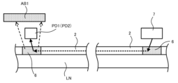
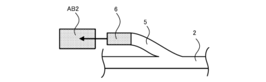
- Patent Document 1 also proposes arranging a light absorbing member AB1 such as a metal behind the light receiving element in order to absorb high-order diffracted light from the grating 6 that cannot be received by the light receiving element PD1 (PD2) and the multiple reflected light thereof, as shown in Figure 2. It also discloses a configuration in which a grating 6 is arranged at the tip of a branching waveguide 5 branching off from an optical waveguide 2, and a light absorbing member AB2 is arranged downstream of the grating 6 in order to absorb noise light leaking from the grating 6, as shown in Figure 3.
- a light absorbing member AB1 such as a metal behind the light receiving element
- an optical component OB such as an optical fiber or lens LEN is attached to an optical waveguide element having a substrate 1 on which a folded optical waveguide 2 is formed.
- inspection light L0 is incident from a specific lens LEN, and the optical element OB is adjusted so that the light receiving sensitivity of the monitor PD provided on the optical waveguide element chip is maximized.
- the light absorbing members (AB1, AB2) When the light absorbing members (AB1, AB2) are arranged in the positions shown in FIG. 2 or FIG. 3, it is suitable for removing noise light after passing through the monitor PD.
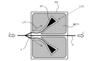
- the position of the monitor PD in the structure of the optical waveguide element with a folded optical waveguide as shown in FIG. 4, the position of the monitor PD is close to the input waveguide end of the optical waveguide 2, so the leakage light of the input light (see symbol LT2 in FIG. 5) is likely to enter the monitor (PD1, PD2).
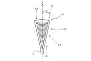
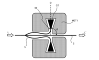
- the diffraction grating GT is designed so that light waves traveling in the direction of arrow A are bounced up directly above the diffraction grating GT (perpendicular to the drawing), and is optimized with the light receiving surface of the light receiving element PD.
- the angle ⁇ of the diffraction grating fanning out from the arrow A is set to about 7°.
- the problem that the present invention aims to solve is to provide an optical waveguide element that solves the problems described above and reduces the noise light that enters the light receiving element. It is also to provide an optical modulation device and an optical transmission device that use this optical waveguide element.
- An optical waveguide element including a substrate having an optical waveguide formed thereon, the optical waveguide having a main waveguide and a branch waveguide branching off from a part of the main waveguide, the optical waveguide including a diffraction grating disposed at an end of the branch waveguide, a light receiving element disposed on the substrate for receiving light waves diffracted by the diffraction grating, and a metal film disposed on the substrate to surround the diffraction grating.
- the metal film is characterized in that it is a part of an electrode formed on the substrate.
- the metal film is disposed at least on a straight line connecting the diffraction grating and a branch point where the branch waveguide branches off from the main waveguide.
- the optical waveguide element described in (1) above is characterized in that the angle formed by the extension direction of the main waveguide at the branch point where the branch waveguide branches off from the main waveguide and the tangent direction at the end of the curve formed by the branch waveguide is 40 degrees or more.
- the metal film has a pattern having a portion along a part of the edge of the light receiving element where the metal film is not disposed when the substrate is viewed in a plan view, and the pattern also serves as a positioning means for the light receiving element.
- the metal film comprises a first metal film having at least a portion that is disposed inside the light receiving element when the substrate is viewed in plan, and a second metal film that is composed only of a portion that is disposed outside the light receiving element and has a portion that surrounds the first metal film, and the second metal film is configured to be thicker than the first metal film.
- the optical waveguide element described in (6) above is characterized in that the electrode formed on the substrate is multi-stage, and the first and second metal films are formed from metal films of any of the stages constituting the electrode.
- the thickness of the metal film disposed inside the light receiving element when the substrate is viewed in plan is 2 ⁇ m or less.
- An optical modulation device comprising an optical waveguide element according to any one of (1) to (8) above, a housing for housing the optical waveguide element, and an optical fiber for inputting and outputting light waves to and from the optical waveguide element.
- the optical modulation device described in (9) above is characterized in that a modulation electrode that modulates the light wave propagating through the optical waveguide is provided on the substrate, and an electronic circuit that amplifies the modulation signal input to the modulation electrode is provided inside or outside the housing.
- An optical transmission device comprising the optical modulation device described in (10) above and an electronic circuit that outputs a modulation signal that causes the optical modulation device to perform a modulation operation.
- the present invention provides an optical waveguide element having a substrate on which an optical waveguide is formed, the optical waveguide having a main waveguide and a branch waveguide branching from a part of the main waveguide, a diffraction grating arranged at the end of the branch waveguide, a light receiving element arranged on the substrate for receiving light waves diffracted by the diffraction grating, and a metal film arranged on the substrate so as to surround the diffraction grating. Therefore, for example, stray light such as leakage light emitted from the branch part between the main waveguide and the branch waveguide is absorbed by the metal film and is prevented from reaching the diffraction grating. As a result, it is possible to provide an optical waveguide element that reduces noise light entering the light receiving element. It is also possible to provide an optical modulation device and an optical transmission device using an optical waveguide element having such an effect.
- FIG. 1 is a plan view showing an example of an optical waveguide element described in Patent Document 1.
- FIG. 1 is a side view illustrating an optical waveguide and a grating in the optical waveguide element described in Patent Document 1.
- FIG. 1 is a plan view illustrating a state in which a light absorbing member (electrode or the like) is disposed after a grating in the optical waveguide element described in Patent Document 1.
- 11 is a plan view illustrating the position adjustment of the optical member OB with respect to the optical waveguide 2.
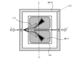
- FIG. 1A and 1B are diagrams illustrating a state in which leakage light is incident on a diffraction grating provided in a branching waveguide.
- FIG. 1A and 1B are diagrams illustrating a state in which leakage light is incident on a diffraction grating provided in a branching waveguide.
- FIG. 2 is a diagram illustrating an example of a diffraction grating used in the optical waveguide element of the present invention.
- 1A to 1C are diagrams illustrating a first embodiment of an optical waveguide element according to the present invention.
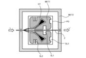
- 1A to 1C are diagrams illustrating a second embodiment of the optical waveguide element of the present invention. This is a cross-sectional view taken along dashed line C-C' in Figure 8.
- FIG. 8 is a diagram for explaining the arrangement angle of the diffraction grating in FIG. 7 .
- FIG. 11 is a diagram showing an application example of FIG. 10 .
- FIG. 9 is a diagram for explaining an example in which slits are provided in the first metal film MET1 in the embodiment of FIG. 8.
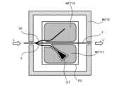
- FIG. 13A and 13B are diagrams illustrating an example in which a diffraction grating is disposed only in one of two branching waveguides.
- 1 is a diagram showing how a part of a light wave branched by a multi-mode interference waveguide (MMI) 20 is guided to a light receiving element PD.
- MMI multi-mode interference waveguide
- 1 is a diagram illustrating an optical waveguide element in which an input section and an output section for optical waves are formed on opposite sides of a substrate 1 (chip).
- 1 is a diagram illustrating an optical waveguide element in which an input section and an output section for optical waves are formed on adjacent sides of a substrate 1 (chip).
- 1 is a plan view showing an optical modulation device and an optical transmission device according to the present invention;
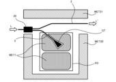
- the present invention provides an optical waveguide element comprising a substrate 1 on which an optical waveguide 2 is formed, the optical waveguide 2 having a main waveguide 2 and a branch waveguide 5 branching off from a part of the main waveguide, a diffraction grating GT arranged at an end of the branch waveguide 2, a light receiving element PD arranged on the substrate for receiving light waves diffracted by the diffraction grating, and a metal film MET1 arranged on the substrate so as to surround the diffraction grating.
- a substrate having an electro-optic effect such as lithium niobate (LN), lithium tantalate (LT), or PLZT (lead lanthanum zirconate titanate), a vapor-deposited film made of these materials, or a composite substrate in which these materials are bonded to a substrate of a different type can be used.
- various materials such as semiconductor materials and organic materials can also be used.
- One method of forming an optical waveguide is to use a rib-type optical waveguide in which the portion of the substrate corresponding to the optical waveguide is convex by etching the surface of the substrate other than the optical waveguide and forming grooves on both sides of the optical waveguide.By using a horizontal slot waveguide in which a slot waveguide structure is formed in the thickness direction by thinning the substrate, it is possible to reduce bending loss. It is also possible to form an optical waveguide by forming a high refractive index portion on the substrate surface using a thermal diffusion method, a proton exchange method, etc. of Ti, etc. It is also possible to form a composite optical waveguide by diffusing a high refractive index material into a rib-type optical waveguide portion. In particular, when using a folded optical waveguide, a convex waveguide with a width or height of about 1 ⁇ m, which has strong light confinement, is used.
- the substrate on which the optical waveguide is formed is thinned by grinding and polishing to a thickness of 10 ⁇ m or less, more preferably 5 ⁇ m or less, and even more preferably less than 1 ⁇ m (the lower limit of the thickness is preferably 0.3 ⁇ m or more), or a thinned substrate is produced using the smart cut method (a method of thinning by ion implantation peeling).
- the height of the rib-type optical waveguide is preferably set to 1 ⁇ m or less. It is also possible to form a vapor-grown film on a holding substrate with a thickness of about the same as the above-mentioned substrate, and process the film into the shape of the above-mentioned optical waveguide.
- the substrate (thin plate, thin film) on which the optical waveguide is formed is bonded to a holding substrate by direct bonding or via an adhesive layer such as resin to increase mechanical strength.
- a holding substrate for direct bonding a material with a lower refractive index than the optical waveguide or the substrate on which the optical waveguide is formed and a thermal expansion coefficient close to that of the optical waveguide, such as quartz, is preferably used.
- an intermediate layer with a low refractive index it is also possible to use the same material as the substrate on which the optical waveguide is formed, such as an LN substrate, as a reinforcing substrate, or to use a substrate with a high refractive index such as silicon as the holding substrate.
- the "substrate” in this invention is a concept that includes this holding substrate.
- the optical waveguide element of the present invention is characterized in that a metal film is disposed so as to surround a diffraction grating disposed at an end of a branching waveguide.
- 7 is a plan view for explaining a first embodiment of the optical waveguide element of the present invention.
- the lower part of the light receiving element PD is invisible, but the light receiving element PD is made transparent so that the metal film MET1 and the diffraction grating GT can be seen.
- the symbol L indicates a light wave incident on the optical waveguide 2 in the region of interest, and the symbol L' indicates a light wave exiting from the optical waveguide 2.
- the diffraction grating GT may be subject to leakage light LT1 from the branch point where the main waveguide 2 and the branch waveguide 5 branch, and leakage light LT2 from the input section of the optical waveguide 2 formed in the optical waveguide element.
- leakage light LT1 occurs in the vicinity of the diffraction grating GT, by arranging the metal film MET1 so as to surround the diffraction grating, it is possible to reliably suppress the leakage light LT1 from entering the diffraction grating. In particular, as shown in FIG.
- the metal film MET1 is arranged at least on the straight line connecting the branch point where the branch waveguide 5 branches off from the main waveguide 2 and the diffraction grating GT, thereby suppressing the leakage light LT1 from the branch point from reaching the diffraction grating GT.
- the metal layer MET1 can also prevent leakage light LT2 from the input portion of the optical waveguide element from reaching the diffraction grating GT. Furthermore, in order to effectively suppress leakage light (stray light) generated from places other than the branch point, such as leakage light LT2, at the diffraction grating GT, it is also possible to arrange a second metal film to surround the first metal film MET1, as shown in Figure 8.
- the first metal film MET1 is a metal film having at least a portion disposed inside the light receiving element PD when the substrate 1 is viewed in plan view. As will be described later, the first metal film MET1 may have a portion protruding outside the light receiving element PD.
- the second metal film MET2 is a metal film that is composed only of a portion that is disposed outside the light receiving element PD and that has a portion that surrounds the first metal film MET1.
- FIG. 9 shows a schematic cross-sectional view taken along dashed line CC' in FIG.
- the substrate 1 on which the optical waveguide 2 is formed is formed on the upper surface of the holding substrate 3.
- Branch waveguides 5 are formed to sandwich the central main waveguide 2, and around the optical waveguide 2 and the branch waveguide 5, any dielectric material having a lower refractive index than the substrate 1, whether organic or inorganic, is used.
- a resin such as a resist, which has a small Young's modulus and is easy to pattern, is preferably used, for example, a polyamide resin, a melamine resin, a phenol resin , an amino resin, or an epoxy resin.
- SiO2 , SiN , Al2O3 , MgF, La2O3 , ZnO, MgO, CaF2 , Y2O3 , or the like is used.
- this buffer layer BF it is possible to reduce the scattering loss of light in the optical waveguide 2 and the branching waveguide 5, and as a result, the optical loss characteristics are improved.
- the first metal film MET1 is arranged to sandwich the branching waveguide 5, and a resist RE is arranged to cover the optical waveguide 2. It is also possible to remove the buffer layer and arrange the resist so that it is in contact with the optical waveguide. By forming the resist RE when mounting the light receiving element PD, it is expected that the upper surface of the resist RE can be used to improve installation accuracy (horizontal).
- the light receiving element PD is fixed with adhesive AD.
- the light waves traveling upward from the diffraction grating GT (not shown in FIG. 9) arranged at the end of the branching waveguide 5 are incident on the light receiving element PD arranged on the upper side of the substrate 1.
- the light receiving element PD has light receiving surfaces PS with photoelectric conversion function provided in two locations corresponding to the two diffraction gratings.
- the two light receiving surfaces PS may be configured to output monitor signals separately, but if necessary, the two light receiving surfaces can be integrally formed as a single light receiving surface, and the two light waves obtained from the two diffraction gratings can be combined and output as a monitor signal.
- the first metal film MET1 and the second metal film MET2 are not particularly limited as long as they are made of a material that can absorb light waves, such as Au.
- a control electrode such as a modulation electrode or a DC bias electrode, that is disposed on the substrate of the optical waveguide element
- the control electrode is formed by stacking multiple electrode layers in a multi-stage structure (such as a staircase structure in which the protruding end portions of each stage are positioned at different positions), it is also possible to configure the first metal film and the second metal film by combining different stages (electrode layers).
- the thickness of the first metal film MET1 is 2 ⁇ m or less, more preferably 1 ⁇ m or less, and even more preferably less than 0.7 ⁇ m.
- the lower limit of the thickness is preferably 0.3 ⁇ m or more. Since the first metal film MET1 has a portion located below the light receiving element PD, a thinner thickness makes it possible to place a permanent resist on the metal film MET1 using a permanent resist or the like, and to mount the light receiving element and the optical waveguide in parallel with high precision. Note that if the metal film is too thin, the light absorption performance decreases, so it is preferable to ensure the above-mentioned thickness.
- the first metal film MET1 is placed close to the main waveguide 2 and the branching waveguide 5, so it is necessary to precisely control the distance between the optical waveguide and the metal film. For this reason, an electron beam (EB) lithography device is used to pattern the EB resist.
- EB resist is also used to form the electrode layer of the first or specific stage of the control electrode (modulation electrode or DC bias electrode) placed close to the optical waveguide. For this reason, it is preferable to form the first metal layer in accordance with the formation of the electrode layer of the stage in which EB resist is used for the control electrode.
- the thickness of the second metal film MET2 is thicker than the thickness of the first metal film MET1.
- the upper surface of the second metal film MET2 is located at a position higher than the position of the lower surface of the light receiving element PD. This is because, when leakage light (stray light) from outside the second metal film enters the area of the second metal film MET2, not only the light waves propagating inside the substrate 1 but also the light waves propagating in the space above the substrate 1 can be blocked efficiently.
- the thickness of the second metal film MET2 is thick in order to improve the electrical bandwidth and high frequency characteristics.
- a pattern can be formed in the photoresist using an ultraviolet exposure machine, just as in the case of the control electrode, to give it a thickness of, for example, about 8 to 30 ⁇ m.
- the angle ⁇ of the diffraction grating GT arranged at the end 50 of the branch waveguide 5 is set to, for example, 40 degrees or more.
- the angle ⁇ is 40 degrees or more, the angle at which the leakage light LT1 emitted from the branch point of the branch waveguide 5 intersects with the tangent direction D of the diffraction grating GT changes from 0 degrees to 90 degrees. Therefore, the amount of stray light introduced from the diffraction grating to the light receiving element PD is reduced, like the stray light (IL2 or IL3) incident on the diffraction grating GT in FIG. 6.
- the angle ⁇ of the diffraction grating GT becomes extremely important.
- Figures 15 and 16 are application examples of the optical waveguide element of the present invention.
- a diffraction grating GT is provided on only one of the two branch waveguides.
- a first metal film MET11 is provided to surround the diffraction grating.
- a metal film MET10 is formed to cover the other branch waveguide, and absorbs the light waves propagating through that waveguide.
- the light receiving element PD only needs to have a light receiving surface that corresponds to at least the diffraction grating GT, and a light receiving element with two light receiving surfaces may be used to reduce the number of parts.
- FIG. 16 it is formed using a multimode interference waveguide (MMI) 20 of the branching waveguide 5. Even in such a case, it is possible to attach a diffraction grating GT to the end of the branching waveguide 5. Also, a first metal film MET1 is arranged to surround the diffraction grating GT. Naturally, if the light receiving element has multiple light receiving surfaces, it is preferable to form a metal film under the unused light receiving surfaces. Furthermore, a second metal film (MET20, MET21) may also be formed to surround the light receiving element PD.
- MMI multimode interference waveguide
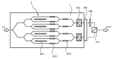
- the configuration of the optical waveguide element of the present invention is effective not only in the case of using a folded optical waveguide as shown in FIG. 4, but also in the case of an optical waveguide element in which an input part (Lin) and an output part (Lout) of the optical wave are formed on the opposing sides of the substrate 1 (chip) as shown in FIG. 17, or in the case of an input part and an output part of the optical wave are formed on the adjacent sides of the substrate 1 (chip) as shown in FIG. 18.
- the input part is disposed away from the light receiving element PD, but when multiple Mach-Zehnder type optical waveguides are used, more leakage light (stray light) is generated than in the branching and multiplexing parts of each Mach-Zehnder type optical waveguide.
- it is extremely important to suppress the leakage light from entering the diffraction grating for example, to position the optical component OB in a state in which a predetermined voltage is applied to the modulation electrode RF1 and the DC bias electrodes (DC1, DC2) and the amount of light received by the light receiving element PD is optimized.
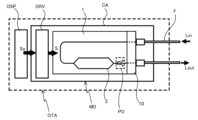
- a compact optical modulation device MD can be provided by housing the optical waveguide element (substrate 1) of the present invention in a housing CA made of metal or the like and connecting the outside of the housing to the optical waveguide element with an optical fiber F.
- Reference numeral 10 denotes a reinforcing member superimposed on substrate 1 along the end face of substrate 1, and is used when directly joining an optical component such as an optical fiber to the end face of substrate 1.
- An electronic circuit that outputs a modulation signal S0 that causes the optical modulation device MD to perform a modulation operation can be connected to the optical modulation device MD to configure an optical transmission device OTA. Since the modulation signal S to be applied to the optical waveguide element needs to be amplified, a driver circuit DRV is used.
- the driver circuit DRV and the digital signal processor DSP can be placed outside the housing CA, but can also be placed inside the housing CA. In particular, by placing the driver circuit DRV inside the housing, the propagation loss of the modulation signal from the driver circuit can be further reduced and a wider bandwidth can be achieved.
- an optical waveguide element that reduces the noise light that enters the light receiving element. It is also possible to provide an optical modulation device and an optical transmission device that use this optical waveguide element.
- Substrate 2 Optical waveguide 5 Branching waveguide (monitoring optical waveguide) GT Diffraction grating MET1 First metal film MET2 Second metal film LT1, LT2 Leakage light
Landscapes
- Physics & Mathematics (AREA)
- Engineering & Computer Science (AREA)
- General Physics & Mathematics (AREA)
- Optics & Photonics (AREA)
- Microelectronics & Electronic Packaging (AREA)
- Nonlinear Science (AREA)
- Chemical & Material Sciences (AREA)
- Ceramic Engineering (AREA)
- Crystallography & Structural Chemistry (AREA)
- Optical Integrated Circuits (AREA)
Abstract
Description
光導波路素子を小型化するため、折り返し光導波路2のモードフィールド径(MFD)が1μm程度と小さいため、光導波路2の端部にはスポットサイズ変換部SSCを設け、MFDを3μm以上に広げることが行われている。
一般的に、回析格子の矢印Aから扇状に広がっている角度αは、7°程度の角度に設定される。
このため、図5の主導波路2と分岐導波路5との分岐部からの漏れ光LT1や、光導波路2への入力光の漏れ光LT2は、回折格子GTで跳ね上げられ、受光素子のノイズとなり易い。
(1) 光導波路を形成した基板を備えた光導波路素子において、該光導波路が、主導波路と該主導波路の一部から分岐する分岐導波路とを有し、該分岐導波路の端部に配置された回折格子と、該基板上に配置され、該回折格子で回折される光波を受光するための受光素子と、該回折格子を取り囲むように、該基板上に配置される金属膜とを備えることを特徴とする。
本発明は、図7及び8に示すように、光導波路2を形成した基板1を備えた光導波路素子において、該光導波路2が、主導波路2と該主導波路の一部から分岐する分岐導波路5とを有し、該分岐導波路2の端部に配置された回折格子GTと、該基板上に配置され、該回折格子で回折される光波を受光するための受光素子PDと、該回折格子を取り囲むように、該基板上に配置される金属膜MET1とを備えることを特徴とする。
また、半導体材料や有機材料など種々の材料も利用可能である。
また、Tiなどを熱拡散法やプロトン交換法などで基板表面に高屈折率部分を形成することで光導波路を形成することも可能である。リブ型光導波路部分に高屈折率材料を拡散するなど、複合的な光導波路を形成することも可能である。特に、折り曲げた光導波路を使用する場合には、光閉じ込めの強い、幅又は高さが1μm程度の凸状導波路を用いる。
図7は、本発明の光導波路素子に係る第1の実施例を説明する平面図である。本来であれば、受光素子PDの下部は見えない構造であるが、受光素子PDを透明化し、金属膜MET1と回析格子GTが見えるように図示している。また、符号Lは着目している領域の光導波路2に入射する光波であり、符号L’は該光導波路2から出射する光波を示す。
さらに、漏れ光LT2のように、分岐点以外の場所から発生する漏れ光(迷光)で、回折格子GTに漏れ光を効果的に抑制するため、図8に示すように、第1の金属膜MET1を取り囲むように第2の金属膜を配置することも可能である。
また、第2の金属膜MET2は、受光素子PDの外側に配置される部分のみから構成され、かつ前記第1の金属膜MET1を取り囲む部分を備えた金属膜である。
図9では、光導波路2を形成した基板1は、保持基板3の上面に形成されている。中央の主導波路2を挟むように分岐導波路5が形成され、光導波路2と分岐導波路5の周囲には、基板1よりも屈折率の低い誘電体であれば有機/無機を問わないが、有機誘電体であれば、レジストのような樹脂で、ヤング率が小さく、パターニングしやすいものが望ましく、例えば、ポリアミド系樹脂、メラミン系樹脂、フェノール系樹脂、アミノ系樹脂、エポキシ系樹脂などの材料を設ける。また、無機誘電体であれば、SiO2、SiN、Al2O3、MgF、La2O3、ZnO、MgO、CaF2、Y2O3などを設ける。
このバッファ層BFを設けることにより、光導波路2と分岐導波路5の光の散乱損失を低減させることができ、その効果により光ロス特性が向上する。
また、制御電極を複数の電極層を積み上げ多段状(階段状などのように、各段毎に突出している端部の位置が異なる状態)に形成する場合は、第1の金属膜と第2の金属膜を異なる段(電極層)の組合せで構成することも可能である。
このため、分岐導波路5が主導波路2から分岐した分岐点における主導波路2の延在方向(図10の左右方向)と、該分岐導波路5が形成する曲線の端部で回折格子が取り付けられている位置での接線方向Dとが形成する角度θは、例えば40度以上に設定する。角度θが40度以上になると、分岐導波路5の分岐点から放射される漏れ光LT1と回折格子GTの接線方向Dとが交わる角度が、0度から90度へと変化する。このため、図6の回折格子GTに入射する迷光(IL2又はIL3)のように、回折格子から受光素子PDへ導入される迷光の量が減少することとなる。
特に、分岐導波路の分岐点から回折格子GTまでは、直線距離で約350μmと近いため、回析格子GTの角度θは、極めて重要となる。
2 光導波路
5 分岐導波路(モニタ用光導波路)
GT 回折格子
MET1 第1の金属膜
MET2 第2の金属膜
LT1,LT2 漏れ光
Claims (11)
- 光導波路を形成した基板を備えた光導波路素子において、
該光導波路が、主導波路と該主導波路の一部から分岐する分岐導波路とを有し、
該分岐導波路の端部に配置された回折格子と、
該基板上に配置され、該回折格子で回折される光波を受光するための受光素子と、
該回折格子を取り囲むように、該基板上に配置される金属膜とを備えることを特徴とする光導波路素子。 - 請求項1に記載の光導波路素子において、該金属膜は、該基板に形成された電極の一部で構成することを特徴とする光導波路素子。
- 請求項1に記載の光導波路素子において、該金属膜は、該分岐導波路が該主導波路から分岐した分岐点と該回折格子とを結ぶ直線上に少なくとも配置されていることを特徴とする光導波路素子。
- 請求項1に記載の光導波路素子において、該分岐導波路が該主導波路から分岐した分岐点における該主導波路の延在方向と、該分岐導波路が形成する曲線の該端部における接線方向とが形成する角度は40度以上であることを特徴とする光導波路素子。
- 請求項1に記載の光導波路素子において、該金属膜は、該基板を平面視した場合に、該受光素子の縁の一部に沿って該金属膜が配置されていない部分を有するパターンを備え、該パターンが該受光素子の位置決め手段を兼ねていることを特徴とする光導波路素子。
- 請求項1に記載の光導波路素子において、該金属膜は、該基板を平面視した場合に、該受光素子の内側に配置される部分を少なくとも有する第1の金属膜と、該受光素子の外側に配置される部分のみから構成され、かつ前記第1の金属膜を取り囲む部分を備えた第2の金属膜を有し、前記第2の金属膜は、前記第1の金属膜より厚みが大きくなるように設定されていることを特徴とする光導波路素子。
- 請求項6に記載の光導波路素子において、該基板に形成された電極が多段状であり、前記第1及び第2の金属膜は、該電極を構成するいずれかの段の金属膜で形成されていることを特徴とする光導波路素子。
- 請求項1に記載の光導波路素子において、該基板を平面視した場合に該受光素子の内側に配置される該金属膜の厚みは、2μm以下であることを特徴とする光導波路素子。
- 請求項1乃至8のいずれかに記載の光導波路素子と、該光導波路素子を収容する筐体と、該光導波路素子に光波を入出力する光ファイバとを有することを特徴とする光変調デバイス。
- 請求項9に記載の光変調デバイスにおいて、該光導波路を伝搬する光波を変調する変調電極を該基板に設け、該変調電極に入力する変調信号を増幅する電子回路を該筐体の内部又は外部に有することを特徴とする光変調デバイス。
- 請求項10に記載の光変調デバイスと、該光変調デバイスに変調動作を行わせる変調信号を出力する電子回路とを有することを特徴とする光送信装置。
Priority Applications (2)
| Application Number | Priority Date | Filing Date | Title |
|---|---|---|---|
| CN202380024095.8A CN118786373A (zh) | 2023-02-10 | 2023-02-10 | 光波导元件、使用光波导元件的光调制器件及光发送装置 |
| PCT/JP2023/004535 WO2024166351A1 (ja) | 2023-02-10 | 2023-02-10 | 光導波路素子とそれを用いた光変調デバイス並びに光送信装置 |
Applications Claiming Priority (1)
| Application Number | Priority Date | Filing Date | Title |
|---|---|---|---|
| PCT/JP2023/004535 WO2024166351A1 (ja) | 2023-02-10 | 2023-02-10 | 光導波路素子とそれを用いた光変調デバイス並びに光送信装置 |
Publications (1)
| Publication Number | Publication Date |
|---|---|
| WO2024166351A1 true WO2024166351A1 (ja) | 2024-08-15 |
Family
ID=92262245
Family Applications (1)
| Application Number | Title | Priority Date | Filing Date |
|---|---|---|---|
| PCT/JP2023/004535 Ceased WO2024166351A1 (ja) | 2023-02-10 | 2023-02-10 | 光導波路素子とそれを用いた光変調デバイス並びに光送信装置 |
Country Status (2)
| Country | Link |
|---|---|
| CN (1) | CN118786373A (ja) |
| WO (1) | WO2024166351A1 (ja) |
Citations (8)
| Publication number | Priority date | Publication date | Assignee | Title |
|---|---|---|---|---|
| JPH09311232A (ja) * | 1996-05-21 | 1997-12-02 | Hitachi Ltd | 光導波路、その製造方法および光モジュール |
| JP2004163675A (ja) * | 2002-11-13 | 2004-06-10 | Ricoh Co Ltd | モニタ付有機導波路型光変調器および光変調装置および光集積回路 |
| US20170168234A1 (en) * | 2015-12-09 | 2017-06-15 | Coriant Advanced Technology, LLC | Shielded photonic integrated circuit |
| US20170192171A1 (en) * | 2016-01-06 | 2017-07-06 | Coriant Advanced Technology, LLC | Integrated on-chip polarizer |
| JP2017191178A (ja) * | 2016-04-12 | 2017-10-19 | 住友電気工業株式会社 | 光送信器 |
| JP2018173604A (ja) * | 2017-03-31 | 2018-11-08 | 住友大阪セメント株式会社 | 光変調器 |
| WO2020213067A1 (ja) * | 2019-04-16 | 2020-10-22 | 日本電信電話株式会社 | 光合波回路および光源 |
| JP2021162642A (ja) * | 2020-03-31 | 2021-10-11 | 住友大阪セメント株式会社 | 光導波路素子とそれを用いた光変調デバイス並びに光送信装置 |
-
2023
- 2023-02-10 WO PCT/JP2023/004535 patent/WO2024166351A1/ja not_active Ceased
- 2023-02-10 CN CN202380024095.8A patent/CN118786373A/zh active Pending
Patent Citations (8)
| Publication number | Priority date | Publication date | Assignee | Title |
|---|---|---|---|---|
| JPH09311232A (ja) * | 1996-05-21 | 1997-12-02 | Hitachi Ltd | 光導波路、その製造方法および光モジュール |
| JP2004163675A (ja) * | 2002-11-13 | 2004-06-10 | Ricoh Co Ltd | モニタ付有機導波路型光変調器および光変調装置および光集積回路 |
| US20170168234A1 (en) * | 2015-12-09 | 2017-06-15 | Coriant Advanced Technology, LLC | Shielded photonic integrated circuit |
| US20170192171A1 (en) * | 2016-01-06 | 2017-07-06 | Coriant Advanced Technology, LLC | Integrated on-chip polarizer |
| JP2017191178A (ja) * | 2016-04-12 | 2017-10-19 | 住友電気工業株式会社 | 光送信器 |
| JP2018173604A (ja) * | 2017-03-31 | 2018-11-08 | 住友大阪セメント株式会社 | 光変調器 |
| WO2020213067A1 (ja) * | 2019-04-16 | 2020-10-22 | 日本電信電話株式会社 | 光合波回路および光源 |
| JP2021162642A (ja) * | 2020-03-31 | 2021-10-11 | 住友大阪セメント株式会社 | 光導波路素子とそれを用いた光変調デバイス並びに光送信装置 |
Also Published As
| Publication number | Publication date |
|---|---|
| CN118786373A (zh) | 2024-10-15 |
Similar Documents
| Publication | Publication Date | Title |
|---|---|---|
| JP5012624B2 (ja) | 光導波路素子 | |
| JP4658658B2 (ja) | 光変調器 | |
| JP7585940B2 (ja) | 光導波路素子とそれを用いた光変調デバイス並びに光送信装置 | |
| CN214795475U (zh) | 光波导元件、使用光波导元件的光调制器件及光发送装置 | |
| JP6056800B2 (ja) | 光変調器 | |
| US11892745B2 (en) | Wavelength conversion element and method for manufacturing same | |
| WO2001069308A1 (en) | Optical waveguide modulator with output light monitor | |
| JP2006301612A (ja) | 光変調器 | |
| WO2007122877A1 (ja) | 光変調素子 | |
| JP7054068B2 (ja) | 光制御素子とそれを用いた光変調デバイス並びに光送信装置 | |
| US11442225B2 (en) | Wavelength conversion element and method for manufacturing wavelength conversion element | |
| KR20090093427A (ko) | 표면 플라즈몬 공명을 이용한 전광 스위치 | |
| US6868210B2 (en) | Optical waveguide and their application of the optical communication system | |
| WO2024166351A1 (ja) | 光導波路素子とそれを用いた光変調デバイス並びに光送信装置 | |
| WO2022102053A1 (ja) | 光接続構造、光モジュールおよび光接続構造の製造方法 | |
| CN221378428U (zh) | 光波导元件、使用光波导元件的光调制器件及光发送装置 | |
| JP5133930B2 (ja) | 光変調器モジュール | |
| KR100960078B1 (ko) | 표면 플라즈몬 공명을 이용한 광 아이솔레이터 | |
| WO2024201728A1 (ja) | 光導波路素子とそれを用いた光変調デバイス並びに光送信装置 | |
| WO2025203274A1 (ja) | 光導波路素子及びそれを用いた光変調器並びに光送信装置 | |
| WO2024069952A1 (ja) | 光導波路素子及びそれを用いた光変調デバイス並びに光送信装置 | |
| CN121399531A (zh) | 光波导元件及使用其的光调制器以及光发送装置 | |
| CN111886536A (zh) | 光调制装置 | |
| JP2007286428A (ja) | 光導波路型光変調器及び出力光モニタ付光導波路型光変調器 |
Legal Events
| Date | Code | Title | Description |
|---|---|---|---|
| WWE | Wipo information: entry into national phase |
Ref document number: 202380024095.8 Country of ref document: CN |
|
| 121 | Ep: the epo has been informed by wipo that ep was designated in this application |
Ref document number: 23921180 Country of ref document: EP Kind code of ref document: A1 |
|
| WWE | Wipo information: entry into national phase |
Ref document number: 18851323 Country of ref document: US |
|
| NENP | Non-entry into the national phase |
Ref country code: DE |
|
| 122 | Ep: pct application non-entry in european phase |
Ref document number: 23921180 Country of ref document: EP Kind code of ref document: A1 |