WO2024161641A1 - 生体電気信号計測電極、生体電気信号計測装置及び生体電気信号計測電極の製造方法 - Google Patents
生体電気信号計測電極、生体電気信号計測装置及び生体電気信号計測電極の製造方法 Download PDFInfo
- Publication number
- WO2024161641A1 WO2024161641A1 PCT/JP2023/003629 JP2023003629W WO2024161641A1 WO 2024161641 A1 WO2024161641 A1 WO 2024161641A1 JP 2023003629 W JP2023003629 W JP 2023003629W WO 2024161641 A1 WO2024161641 A1 WO 2024161641A1
- Authority
- WO
- WIPO (PCT)
- Prior art keywords
- dielectric
- conductive
- conductor
- signal measurement
- conductive portion
- Prior art date
- Legal status (The legal status is an assumption and is not a legal conclusion. Google has not performed a legal analysis and makes no representation as to the accuracy of the status listed.)
- Ceased
Links
Images








Classifications
-
- A—HUMAN NECESSITIES
- A61—MEDICAL OR VETERINARY SCIENCE; HYGIENE
- A61B—DIAGNOSIS; SURGERY; IDENTIFICATION
- A61B5/00—Measuring for diagnostic purposes; Identification of persons
- A61B5/24—Detecting, measuring or recording bioelectric or biomagnetic signals of the body or parts thereof
- A61B5/25—Bioelectric electrodes therefor
- A61B5/251—Means for maintaining electrode contact with the body
- A61B5/256—Wearable electrodes, e.g. having straps or bands
Definitions
- the present disclosure relates to a bioelectric signal measurement electrode for forming a bioelectric signal, a bioelectric signal measurement device including the same, and a method for manufacturing the bioelectric signal measurement electrode.
- capacitive electrodes have been known as electrodes for detecting bioelectrical signals such as brainwaves, in which the hair, which acts as a dielectric, is sandwiched between the scalp and the electrode to form a capacitor.
- capacitive electrodes include an amplifier circuit such as an operational amplifier, and are also called active electrodes.
- Patent Document 1 discloses, as an example of an active electrode, "an electrode for detecting bioelectrical signals on the skin surface, comprising a skin contact portion, a metallic substrate, and a coating containing iridium oxide, the coating covering at least a portion of the skin contact portion of the electrode, and the coating comprising a nanostructured surface pattern.”
- the present disclosure has been made in light of the above-mentioned background, and provides a bioelectric signal measuring electrode, a bioelectric signal measuring device, and a method for manufacturing a bioelectric signal measuring electrode that can improve attachment to a living body and test accuracy, and reduce the burden on the living body.
- a bioelectrical signal measurement electrode comprising: a first conductive part that is in direct contact with the skin of a living body and has flexibility to expand and contract while avoiding foreign matter on the skin; a dielectric layered on the first conductive part; and a second conductive part layered on the dielectric, the first conductive part, the dielectric, and the second conductive part form a capacitor on the skin, the first conductive part and the second conductive part are composed of a flat part and a convex part protruding from the surface of the flat part, and the dielectric is formed in an uneven shape between the first conductive part and the second conductive part.
- a bioelectric signal measuring device including a bioelectric signal measuring electrode, the bioelectric signal measuring electrode including a first conductive part that is in direct contact with the skin of a living body and has flexibility to expand and contract while avoiding foreign matter on the skin, a dielectric layered on the first conductive part, and a second conductive part layered on the dielectric, the first conductive part, the dielectric, and the second conductive part forming a capacitor on the skin, the first conductive part and the second conductive part being composed of a flat part and a convex part protruding from the surface of the flat part, and the dielectric being formed in an uneven shape between the first conductive part and the second conductive part, and a processing device connected to the bioelectric signal measuring electrode and transmitting a biosignal received from the bioelectric signal measuring electrode to an external device.
- a method for manufacturing a bioelectrical signal measurement electrode comprising a step of laminating a first conductive portion having flexibility to extend while avoiding foreign objects on the skin, a dielectric selected from materials that generate an alternating current of a predetermined frequency when an alternating electric field is applied, and a second conductive portion sandwiching the dielectric between the first conductive portion to form a capacitor, wherein the first conductive portion and the second conductive portion are formed so that convex portions protrude from the surface of a flat portion, and the dielectric is formed in an uneven shape between the first conductive portion and the second conductive portion.
- the present disclosure provides a bioelectric signal measuring electrode, a bioelectric signal measuring device, and a method for manufacturing a bioelectric signal measuring electrode that can improve attachment to a living body and test accuracy, and reduce the burden on the living body.
- FIG. 1 is a diagram showing a schematic configuration of a bioelectrical signal measuring system 1 according to a first embodiment of the present disclosure.
- FIG. 2 is a cross-sectional view of the bioelectrical signal measurement electrode 120 according to the first embodiment of the present disclosure.
- FIG. 3 is a block diagram showing an example of the configuration of the processing device 130 according to the first embodiment of the present disclosure.
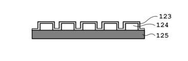
- FIG. 4A is a cross-sectional view of the bioelectrical signal measurement electrode 120 according to the first embodiment of the present disclosure during a manufacturing process.
- FIG. 4B is a cross-sectional view of the bioelectrical signal measurement electrode 120 according to the first embodiment of the present disclosure in a manufacturing process.
- FIG. 1 is a diagram showing a schematic configuration of a bioelectrical signal measuring system 1 according to a first embodiment of the present disclosure.
- FIG. 2 is a cross-sectional view of the bioelectrical signal measurement electrode 120 according to the first embodiment of the present disclosure.
- FIG. 3 is a block diagram showing an example of the
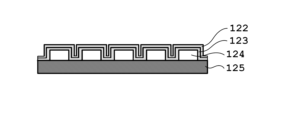
- FIG. 4C is a cross-sectional view of the bioelectrical signal measurement electrode 120 according to the first embodiment of the present disclosure during a manufacturing process.
- FIG. 4D is a cross-sectional view of the bioelectrical signal measurement electrode 120 according to the first embodiment of the present disclosure during a manufacturing process.
- FIG. 4E is a cross-sectional view of the bioelectrical signal measurement electrode 120 according to the first embodiment of the present disclosure during a manufacturing process.
- FIG. 4F is a cross-sectional view of the bioelectrical signal measurement electrode 120 according to the first embodiment of the present disclosure during a manufacturing process.
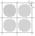
- FIG. 5 is a plan view of the bioelectric signal measurement electrode 120 according to the first embodiment of the present disclosure during a manufacturing process.
- FIG. 6 is a plan view of a manufacturing process of the bioelectric signal measurement electrode 120 according to a modified example of the first embodiment of the present disclosure.
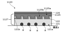
- FIG. 7 is a cross-sectional view of a bioelectrical signal measurement electrode 1120 according to the second embodiment of the present disclosure.
- FIG. 8A is a cross-sectional view of a manufacturing process of a bioelectrical signal measurement electrode 1120 according to the second embodiment of the present disclosure.
- FIG. 8B is a cross-sectional view of the bioelectrical signal measurement electrode 1120 according to the second embodiment of the present disclosure during a manufacturing process.
- FIG. 8C is a cross-sectional view of the bioelectrical signal measurement electrode 1120 according to the second embodiment of the present disclosure during a manufacturing process.
- FIG. 8A is a cross-sectional view of a manufacturing process of a bioelectrical signal measurement electrode 1120 according to the second embodiment of the present disclosure.
- FIG. 8B is a cross-sectional view of the bioelectrical signal measurement electrode 1120 according to
- FIG. 8D is a cross-sectional view of the bioelectrical signal measurement electrode 1120 according to the second embodiment of the present disclosure during a manufacturing process.
- FIG. 8E is a cross-sectional view of the bioelectrical signal measurement electrode 1120 according to the second embodiment of the present disclosure during a manufacturing process.
- FIG . 1 is a diagram showing a schematic configuration of the bioelectric signal measurement system 1 according to the first embodiment of the present disclosure.
- the bioelectric signal measurement system 1 according to the first embodiment is used to measure brain waves as bioelectric signals and analyze the brain state and mental state of the subject P.
- the bioelectric signal measurement system 1 shown in FIG. 1 includes a bioelectric signal measurement device 100 worn on the head of the subject P who receives bioelectric signal measurement, a mobile terminal device (external device) 200 that receives the bioelectric signal measured by the bioelectric signal measurement device 100, and a terminal device (external device) 300 that receives the bioelectric signal under specific conditions.
- FIG. 1 shows the connection relationship for data communication between the bioelectric signal measurement device 100, the mobile terminal device 200, and the terminal device 300.
- the bioelectric signal measuring device 100 includes a main body (headgear) 110 that is attached to the head of the subject P, a plurality of bioelectric signal measuring electrodes 120 arranged inside the main body 110, and a processing device 130 electrically connected to each measuring electrode.
- the main body 110 may be of any shape as long as it can be attached to the head of the subject P, and may be a type that covers the entire head or a type that covers only a part of the head.
- the bioelectric signal measuring electrodes 120 which will be described later with reference to FIG. 2, are attached to a predetermined position on the main body 110 to measure brain waves, and measure brain waves by directly contacting the scalp.
- the processing device 130 which will be described above with reference to FIG. 3, is a device for controlling the operation of the bioelectric signal measuring device 100, and has a structure in which components for executing and controlling each operation are mounted on a circuit board.
- the portable terminal device 200 is a terminal device used by the subject P or a medical professional who performs the measurements.
- the portable terminal device 200 is connected to the processing device 130 of the bioelectric signal measuring device 100 so as to be capable of data communication, and receives brain waves, which are the measured bioelectric signals.
- the portable terminal device 200 also analyzes the received brain waves, and displays the analysis results to the subject P or the medical professional.
- One example of the analysis is understanding the state of the brain of the subject P, his mental state such as depression, and his overall health condition based on the received brain waves.
- the portable terminal device 200 is typically a terminal device capable of wireless communication, such as a smartphone, but is of course not limited to such devices.
- the terminal device may be a feature phone, a personal digital assistant, a PDA, a laptop computer, a desktop computer, a portable game machine, a stationary game machine, or any other device that is capable of the above-mentioned analysis and result display.
- the portable terminal device 200 of the subject P and the portable terminal device 200 of the medical staff may be of the same or different types, and may be connected to the processing device 130 of the bioelectric signal measuring device 100 simultaneously or sequentially so as to be capable of communication.
- the terminal device 300 is a device for receiving brain waves, which are bioelectric signals, in place of the mobile terminal device 200 when the bioelectric signal measuring device 100 is used together with another medical device (not shown).
- the terminal device 300 may be a laptop computer or a desktop computer.
- the medical device in question is, for example, an MRI (Magnetic Resonance Imaging) device, but is not limited to this. That is, when the bioelectric signal measuring device 100 is used for measurement in conjunction with an MRI device that cannot use radio waves in its vicinity, the terminal device 300 connected by wire to the bioelectric signal measuring device 100 is used to process the bioelectric signal.
- MRI Magnetic Resonance Imaging
- the terminal device 300 is connected to the processing device 130 of the bioelectric signal measuring device 100 so as to be able to communicate data, and receives brain waves, which are measured bioelectric signals. Furthermore, the terminal device 300 also analyzes and displays the received brain waves.
- the medical device is an MRI device
- EEG measurement is performed by the bioelectrical signal measuring device 100 while the MRI examination is being performed.
- the results of the EEG measurement are then displayed on the terminal device 300, and various status results of the subject P are provided to the medical staff.
- the bioelectrical signal measuring system 1 according to embodiment 1 envisages a case in which EEG measurement is also performed while an examination is being performed using a general medical device. This makes it possible to correlate the examination using the general medical device with the results of the EEG analysis, allowing the various conditions of the subject P to be understood and predicted in more detail.
- the bioelectric signal measuring device 100 may be fixed to the arm, leg, or chest (in front of the heart) of subject P, and muscle movement may be received as a bioelectric signal and analyzed.
- the bioelectric signal measuring system 1 and the bioelectric signal measuring device 100 are not limited to measuring brain waves in the human body, but can be applied to measure electrical signals of living organisms, including not only humans but also non-human animals.
- the mobile terminal device 200 and the terminal device 300 are connected to the bioelectric signal measuring device 100 so as to be able to communicate data with each other, but the bioelectric signal measuring system 1 may be configured such that only either the mobile terminal device 200 or the terminal device 300 is connected. In other words, the mobile terminal device 200 and the terminal device 300 are not essential components of the bioelectric signal measuring system 1, and it is sufficient if either one is included.
- Fig. 2 is a cross-sectional view of the bioelectrical signal measurement electrode 120 according to the first embodiment of the present disclosure.
- Fig. 2 shows how the bioelectrical signal measurement electrode 120 is in contact with the scalp S and hair H.
- the bioelectrical signal measurement electrode 120 is placed so as to be in direct contact with the scalp S, which is the skin of the subject P.
- the bioelectrical signal measurement electrode 120 has a structure in which a first conductor (first conductor portion) 121, a dielectric 122, a second conductor 123, a resin body 124, a third conductor 125, and an external metal terminal 126 are layered in this order above the scalp S.
- a capacitor 127 is formed by the first conductor 121, the dielectric 122, the second conductor 123, and the third conductor 125.
- the first conductor 121 is in direct contact with the scalp S of the subject P.
- the first conductor 121 also surrounds the hairs H on the scalp S and penetrates between the hairs H.
- the first conductor 121 expands and contracts to avoid the hairs H, which are a type of foreign matter on the scalp S, and is in direct contact with the scalp S.
- the foreign matter refers to substances that are not necessary for measuring bioelectrical signals, and includes not only hair H, but also clumps of sebum and other general debris.
- the first conductor 121 is composed of a flat portion 121a that contacts the scalp S and multiple protruding portions 121b that protrude from the flat portion 121a.
- the first conductor 121 may be, for example, conductive silicone in order to have the flexibility to expand and contract while avoiding foreign matter including hair H as described above.
- the first conductor 121 is made of a material in which a conductive material is contained in silicone rubber, which is a flexible base material. More specifically, the first conductor 121 is a material in which PDMS (dimethylpolysiloxane), which is an example of a base material, contains carbon black or carbon nanotubes (CNT) as a conductive material.
- PDMS dimethylpolysiloxane
- the base material of the first conductor 121 is not limited to the above materials, and various materials can be used as long as they function as a material for forming the capacitor 127 and have the flexibility described above.
- urethane resin polyvinyl alcohol with added borax (slime), starch (kudzu, potato starch, etc.), gellan gum (biological polymer), gel (a mixture of methacrylic acid ester monomer, acrylic acid oligomer, and photopolymerization initiator (photoinitiator)).
- urethane resin polyvinyl alcohol with added borax (slime), starch (kudzu, potato starch, etc.), gellan gum (biological polymer), gel (a mixture of methacrylic acid ester monomer, acrylic acid oligomer, and photopolymerization initiator (photoinitiator)).
- photoinitiator photoinitiator
- the conductive material of the first conductor 121 is not limited to the above materials, but may be a carbon-based material such as CNT or graphite, gold (Au), silver (Ag), copper (Cu), zinc (Zn), sodium chloride (NaCl), platinum (Pt), aluminum (Al), chromium (Cr), molybdenum (Mo), sodium (Na), titanium (Ti), zirconium (Zr), stainless steel, iron (Fe), cobalt (Co), nickel (Ni), or gadolinium (Gd), or a combination of these.
- a combination includes an alloy of two or more materials, coating one material with another material, and mixing two or more materials into a base material.
- the conductive material of the first conductor 121 is biocompatible.
- biocompatibility refers to the property of having affinity with living tissue or organs and not causing foreign body reactions or rejection reactions.
- gold, stainless steel, cobalt, titanium, etc. can be cited as preferable materials.
- Some examples of more specific materials include Ag-(Sn-In-Zn), Ag-Pd-Cu-Au, Ag-Pd-Cu-Zn, Ag-Sn-(Cu) amalgam, Au-Cu, Au-Cu-Ag, Au-Cu-Ag-Pt-Pd, Au-Pt-Pd, Co-Cr, Co-Cr-Fe-Ni, Co-Cr-Mo, Co-Cr-Ni-Cu, Co-Cr-Ni-Mo-Fe, Co-Cr-Ni-W-Fe, Co-Cr-Ta-Ni, Co-Cr-W-Ni, Co-Ni- Cr-Mo, Fe-Cr-Ni-Co, Nd-Fe-B, Ni-Co, Ni-Cr, Pt, Pt-Fe-Nb, Pt-In, Pt-Ir, Sm-Co, SUS301, SUS316, SUS316L, SUS420J1, SUS420J2, SUS430F
- a metal that does not affect MRI measurement which is a medical device, is preferable.
- diamagnetic materials such as gold, silver, copper, zinc, aluminum oxide, or sodium chloride, or paramagnetic materials such as platinum, aluminum, chromium, molybdenum, sodium, titanium, zirconium, or stainless steel are preferable conductive materials.
- a diamagnetic material is a material that, when a strong magnetic field is applied from the outside, has a very weak magnetism in the opposite direction, and when the magnetic field is set to zero, the magnetism becomes zero.
- a paramagnetic material is a material that, when a magnetic field is applied from the outside, has a weak magnetism in the same direction as the magnetic field, but loses magnetism when the magnetic field is set to zero.
- a material that, when a magnetic field is applied from the outside, has a strong magnetism in the same direction as the magnetic field, and remains magnetized even when the magnetic field is set to zero is called a ferromagnetic material.
- Such ferromagnetic materials include iron, cobalt, nickel, and gadolinium, and these materials are highly likely to affect MRI measurement.
- the conductive material of the first conductor 121 is a material that has the above-mentioned biocompatibility and does not affect MRI measurements.
- examples include gold or titanium. More specific examples of materials include Ag-(Sn-In-Zn), Ag-Pd-Cu-Au, Ag-Pd-Cu-Zn, Ag-Sn-(Cu) amalgam, Au-Cu, Au-Cu-Ag, Au-Cu-Ag-Pt-Pd, Au-Pt-Pd, Pt, Pt-Fe-Nb, Pt-In, Pt-Ir, SUS301, SUS316, SUS316L, SUS420J1, SUS420J2, SUS430F, SUS444, SUS447J1, Ta, Ti-15Mo-5Zr-3AI, Ti-6AI-2Nb-1Ta-0.8Mo, Ti-6AI-4V, Ti-6AI-7Nb, and Ti-Mo.
- the thickness of the first conductor 121 is, for example, 50 nm to 1000 nm. However, the thickness of the first conductor 121 may be changed as appropriate depending on the part of the living body with which it comes into contact.
- the dielectric 122 is sandwiched between the two conductors (the first conductor 121 and the second conductor 123) of the capacitor 127 and is formed in an uneven shape.
- the dielectric 122 is a material with predetermined insulating properties. In particular, when an AC electric field acts on the capacitor 126, the material generates an AC current of a predetermined frequency.
- the predetermined frequency is 0.05 Hz to 100 Hz.
- the dielectric 122 has predetermined dielectric relaxation properties depending on the frequency.
- the dielectric relaxation properties are important parameters for measuring weak voltages such as brain waves.
- the effective frequency band for electromyography is around 5 Hz to 500 Hz
- the effective frequency band for electrocardiography is around 0.05 Hz to 100 Hz.
- the dielectric 122 is made of, for example, a polymer-based material. Specifically, the dielectric 122 is made of parylene, a type of polymer obtained from paraxylene. Parylene includes Parylene N, Parylene C, Parylene D, Parylene HT, and Parylene C-UVF, among others. Parylene C is particularly preferred in view of its large electrostatic dissipation factor (corresponding to the above-mentioned dielectric relaxation characteristics) and small dielectric constant.
- a photosensitive polyimide coating agent, a fluorine-based coating agent, or PDMS can also be used, and the fluorine-based coating agent has a large electrostatic dissipation factor and is considered to be a more preferred material.
- the thickness of the dielectric 122 is an important parameter for measuring weak brain waves. This will be discussed in more detail when explaining the capacitor 126 below. For example, it is between 100 nm and 1000 nm. Specifically, when Parylene C is used as the dielectric 122, the thickness of the dielectric 122 is approximately 500 nm. However, the thickness of the dielectric 122 may be changed as appropriate depending on the part of the living body with which it comes into contact.
- the second conductor 123 does not come into direct contact with the scalp S, and is therefore made of a single metal in order to improve the efficiency of extracting electrical signals.
- the second conductor 123 is made of a gold/titanium laminate.
- the second conductor 123 is also formed in an uneven shape so as to follow the shape of the dielectric.
- the second conductor 123 protrudes from the surface of the third conductor 125, which is the flat part of the electrode plate (second conductive part) of the capacitor 127, and corresponds to the convex part of the electrode plate.
- the second conductor 123 is not limited to the above materials, but may be silver, copper, zinc, aluminum oxide, sodium chloride, platinum, aluminum, chromium molybdenum, sodium, titanium, zirconium, stainless steel, iron, cobalt, nickel chromium, tantalum, niobium, tungsten, or gadolinium, or a combination of these.
- a combination includes an alloy of two or more materials, or a laminate of two or more materials.
- the material for the second conductor 123 is preferably a metal that does not affect the MRI measurement, which is a medical device, since it is anticipated that electroencephalogram measurements will be performed while MRI measurements are being performed.
- preferred materials are diamagnetic materials such as gold, silver, copper, zinc, aluminum oxide, or sodium chloride, or paramagnetic materials such as platinum, aluminum, chromium, molybdenum, sodium, titanium, zirconium, or stainless steel.
- the resin body 124 is disposed between the second conductor 123 and the third conductor 125.
- a plurality of through holes 124a are formed in the resin body 124.
- the through holes 124a of the resin body 124 are filled with the first conductor 121, the dielectric 122, and the second conductor 123.
- the material of the resin body 124 may be, for example, a resist material. More specifically, SU-8, which is a negative photoresist, is used as the material of the resin body 124 in order to easily form the shape of the resin body 124.
- the material of the resin body 124 is not limited to the above.
- the thickness of the resin body 124 is, for example, 100 ⁇ m to 1000 ⁇ m. However, the thickness of the resin body 124 may be changed as appropriate depending on the characteristics of the bioelectrical signal to be measured.
- the third conductor 125 does not need to be flexible since it does not come into direct contact with the scalp S, and a relatively hard conductive substrate can be used in consideration of the manufacturing process of the bioelectrical signal measurement electrode 120.
- a flat silicon substrate can be used as the third conductor 125.
- the third conductor 125 corresponds to the flat part of the electrode plate (second conductive part) of the capacitor 127.
- other materials can also be used for the third dielectric 125 as long as they can be processed by MEMS, and for example, titanium, titanium alloys, molybdenum, tantalum, or niobium can be used.
- the third conductor 125 together with the second conductor 123, functions as one side electrode plate (second conductive part) of the capacitor 127 described below.
- the reason for this structure is to provide the third conductor 125 with the same thickness and characteristics as the first conductor 121, which functions as the opposite side electrode plate (first conductive part) of the capacitor described below.
- the thickness of the third conductor 125 is, for example, 10 ⁇ m to 1000 ⁇ m.
- the external metal terminal 126 is a terminal for connecting wiring leading to the processing device 130. Unlike the first conductor 121, the external metal terminal 126 does not come into direct contact with the scalp S, and is therefore made of a single metal to improve the efficiency of drawing out electrical signals.
- the external metal terminal 126 is made of copper.
- the external metal terminal 126 is not limited to the above materials, but may be gold, silver, zinc, aluminum oxide, sodium chloride, platinum, aluminum, chromium molybdenum, sodium, titanium, zirconium, stainless steel, iron, cobalt, nickel, or gadolinium, or a combination of these.
- a combination includes an alloy of two or more materials, or a laminate of two or more materials.
- diamagnetic materials such as gold, silver, copper, zinc, aluminum oxide, or sodium chloride, or paramagnetic materials such as platinum, aluminum, chromium, molybdenum, sodium, titanium, zirconium, or stainless steel are preferable materials.
- the capacitor 127 is composed of the first conductor 121, the dielectric 122, the second conductor 123, and the third conductor 124, which are arranged on the scalp S.
- the scalp S is not used as part of the electrode plate, and the hair H is not used as a dielectric, which is an insulating material. Therefore, even if a reverse current occurs in the bioelectric signal measurement electrode 120 for some reason, the reverse current is stopped by the dielectric 122, which has insulating properties, and the reverse current does not flow to the subject P.
- the capacitor 127 by forming the capacitor 127 with the first conductor 121, the dielectric 122, and the second conductor 123 arranged on the scalp S, it is possible to prevent adverse effects of the reverse current on the subject P.
- the bioelectrical signal measuring device 100 is used to measure weak electroencephalograms, in order to accurately and easily detect the electroencephalograms, the following is important with respect to the structure of the capacitor 127.
- the electric quantity Q of the electroencephalogram to be measured satisfies the following formula (1).
- QS CV...(1)
- S is the cross-sectional area of the capacitor 127 in a direction perpendicular to the lamination direction (the area of the interface between the first conductor 121 and the dielectric 122, or the area of the interface between the dielectric 122 and the second conductor 123).
- C is the capacitance of the capacitor 127.
- V is the voltage generated in the capacitor 127 (the potential difference generated between the first conductor 121 and the second conductor 123).
- the capacitance C of the capacitor 127 is generally given by the following formula (2).
- C ⁇ S/d...(2)
- ⁇ is the relative dielectric constant of the dielectric 122.
- d is the thickness of the dielectric 122.
- S is the cross-sectional area of the capacitor 127 in the direction perpendicular to the lamination direction.
- the electric field strength E in the capacitor 127 is expressed by the following formula (3).
- E V/d...(3)
- V and d are the same as in equations (1) and (2)
- V is the voltage generated in the capacitor 127
- d is the thickness of the dielectric 122.
- the thickness d of the dielectric 122 constituting the capacitor 127 is an important parameter, and that the thickness d must be set within a predetermined range. They have also found that when setting the thickness within the predetermined range, it is important to also take into account the relative dielectric constant ⁇ of the dielectric 122. Based on this idea, it has been derived that the thickness d of the dielectric 122 is preferably set to 100 nm or more and 1000 nm or less. In other words, by setting the thickness of the dielectric 122 in this manner, it is possible to realize the characteristics of the capacitor 127 that can accurately and easily process weak bioelectric signals.
- FIG. 3 is a block diagram showing an example of the configuration of the processing device 130 according to the first embodiment of the present disclosure. Note that the processing device 130 does not need to include all of the components shown in FIG. 3, and may have a configuration in which some components are omitted, or may include other components.
- the processing device 130 includes a memory 131 including RAM, ROM, non-volatile memory, HDD, etc., a processor 132 consisting of a CPU, etc., and a communication interface 133. These components are electrically connected to each other via control lines and data lines.
- Memory 131 includes RAM, ROM, non-volatile memory, and HDD, and functions as a storage unit.
- ROM stores instructions as programs for executing applications related to bioelectrical signal processing and the OS. Such programs are loaded and executed by processor 132.
- RAM is used to write and read data while the programs stored in ROM are being processed by processor 132.
- Non-volatile memory is memory into which data is written and read by the execution of the programs, and data written here is retained even after execution of the programs has ended.
- the processor 132 is composed of an FPGA (Field Programmable Gate Array) or a CPU (microcomputer), and functions as a control unit for controlling other connected components based on various programs stored in the memory 131. Specifically, the processor 132 reads out and executes programs for executing applications related to bioelectrical signal processing and programs for executing the OS from the memory 131.
- the processor 132 may be composed of a single CPU, or may be composed of multiple CPUs.
- the communication interface 133 functions as a communication unit that transmits and receives information (bioelectric signals) between the bioelectric signal measurement electrode 120, the mobile terminal device 200, and the terminal device 300 via a communication processing circuit and an antenna.
- the communication processing circuit performs processing for receiving the bioelectric signal supplied from the bioelectric signal measurement electrode 120.
- the communication processing circuit transmits the received bioelectric signal to the mobile terminal device 200 via the antenna, or transmits the received bioelectric signal to the terminal device 300 via a connected communication wiring.
- the communication processing circuit performs processing based on a wideband wireless communication method such as the LTE method, but it is also possible to process based on a method related to narrowband wireless communication such as wireless LANs such as IEEE802.11 and Bluetooth (registered trademark), or a method related to contactless wireless communication.
- a wideband wireless communication method such as the LTE method
- a method related to narrowband wireless communication such as wireless LANs such as IEEE802.11 and Bluetooth (registered trademark)
- a method related to contactless wireless communication In addition to wireless communication, wired communication can also be used.
- Figures 4A to 4F are cross-sectional views in the manufacturing process of the bioelectric signal measurement electrode 120 according to the first embodiment of the present disclosure.
- Figure 5 is a plan view in the manufacturing process of the bioelectric signal measurement electrode 120 according to the first embodiment of the present disclosure.
- Figures 4A to 4F are partial cross-sectional views in the stacking direction of an intermediate body in each manufacturing process.
- Figure 5 is a partial plan view of the intermediate body at the stage of Figure 4B.
- a silicon wafer that will become the third conductor 125 is prepared ( Figure 4A).
- the silicon wafer functions as a support in this manufacturing process.
- the dimensions of the silicon wafer are determined according to the number of bioelectrical signal measurement electrodes 120 to be manufactured at one time. For example, the diameter of the silicon wafer is 150 nm.
- a resin body 124 is formed on the upper surface of the prepared third conductor 125, which is a silicon wafer (FIG. 4B). Specifically, SU-8 is applied to a thickness of about 250 ⁇ m by spin coating. After that, a plurality of through holes 124a are formed in the resin body 124. More specifically, when SU-8, a negative resist material, is used for the resin body 124, a mask is formed to cover the portion that will become the through holes 124a, and the mask formation surface is irradiated with UV light and further heated. After that, the mask is removed and the portion not irradiated with UV light is also removed, forming the resin body 124 with the through holes 124a formed. In particular, as shown in FIG. 5, within the square surrounded by the dicing line DL, the through holes 124a are formed in a matrix in the region of the bioelectrical signal measurement electrode 120 indicated by the dashed line.
- the second conductor 123 is laminated so as to cover the resin body 124 ( Figure 4C). Specifically, chromium and gold are successively deposited by sputtering. For example, the gold has a thickness of about 30 nm, and the titanium has a thickness of about 15 nm.
- the dielectric 122 is formed so as to cover the second conductor 123 ( Figure 4D). Specifically, a film of parylene C is deposited on the upper surface of the second conductor 123 by chemical vapor deposition (CVD).
- a material with as small a dielectric constant as possible is selected for the dielectric 122, and its thickness is adjusted based on the dielectric constant, the area (cross-sectional area S) of the interface between the first conductor 121 and the dielectric 122, and the strength E of the electric field acting on the capacitor.
- the first conductor 121 is formed so as to cover the dielectric 122 ( Figure 4E). Specifically, the intermediate body with the dielectric 122 formed is inserted into a specified mold, the mold is evacuated, and then conductive silicone is poured in and hardened. Through this process, a capacitor 127 consisting of the first conductor 121, dielectric 122, second conductor 123, and third conductor 125 is formed. The manufacture of the bioelectrical signal measurement electrode 120 is completed.
- an external metal terminal 126 is formed on the back surface (the surface opposite to the surface on which the resin body 124 is formed) of the third conductor 125, which is a silicon wafer (FIG. 4F).
- the third conductor 125 which is a silicon wafer (FIG. 4F).
- a copper film is formed using a known plating technique.
- the wafer is diced along the dicing lines DL shown in FIG. 5, completing the manufacture of the chip-sized bioelectrical signal measurement electrode 120.
- the first conductor 121 may be formed to cover the dielectric 122 after the dicing.
- the order of forming the constituent materials of the bioelectrical signal measurement electrode 120 is not limited to the above and can be changed as appropriate.
- the external metal terminal 125 may be formed before the resin body 124 is formed.
- the film forming method for each component can be selected from various film forming techniques such as electron beam method, vapor deposition, sputtering, plating, etc., and will be selected appropriately according to the material to be formed.
- the resin body 124 is arranged in a dispersed matrix shape, but is not limited to such a shape.
- the resin body 124 may be composed of convex portions 124b formed in a matrix shape (island shape) and connecting portions 124c connecting the convex portions 124b.
- the first conductor 121, the dielectric 122, and the second conductor 123 are also formed on the side and top surfaces of the connecting portions 124c, making it possible to increase the surface area of the dielectric 122. This also improves the characteristics of the capacitor 127 itself.
- the electrode plate at one end of the capacitor 127 is composed of the second conductor 123 and the third conductor 125, but in order to simplify the manufacturing process, it may be composed of only the third dielectric 125. This case will be described below as embodiment 2, but since only the shapes of the respective members are different and the materials used are the same, a description of the same parts as in embodiment 1 will be omitted.
- FIG. 7 is a cross-sectional view of the bioelectric signal measurement electrode 1120 according to embodiment 2 of the present disclosure.
- FIG. 7 shows how the bioelectric signal measurement electrode 1120 is in contact with the scalp S and hair H.
- the bioelectric signal measurement electrode 1120 is placed so as to be in direct contact with the scalp S, which is the skin of the subject P.
- the bioelectric signal measurement electrode 1120 has a structure in which a first conductor 121, a dielectric 122, a third conductor 1125, and an external metal terminal 126 are layered in this order above the scalp S.
- a capacitor 1127 is formed by the first conductor 121, the dielectric 122, and the third conductor 1125.
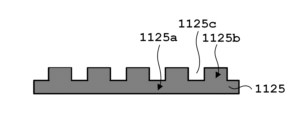
- the resin body is not present, and the third conductor 1125 is formed to take on the convex and matrix shape (island shape) of the resin body. That is, the third conductor 1125 is not formed only in a flat plate shape like the third conductor 125 of the first embodiment, but has unevenness on its surface. In other words, the third conductor 1125 has a flat portion 1125a and a convex portion 1125b protruding from the surface of the flat portion 1125a.
- the flat portion 1125a corresponds to the flat portion of the electrode plate (second conductive portion) of the capacitor 1127
- the convex portion 1125b corresponds to the convex portion of the electrode plate (second conductive portion) of the capacitor 1127.
- FIGS 7A to 7G are cross-sectional views in a manufacturing process of the bioelectric signal measurement electrode 1120 according to the second embodiment of the present disclosure.
- Figure 8 is a plan view in a manufacturing process of the bioelectric signal measurement electrode 1120 according to the second embodiment of the present disclosure. Specifically, Figures 7A to 7G are partial cross-sectional views in the stacking direction of an intermediate body in each manufacturing process. Figure 8 is a partial plan view of the intermediate body at the stage of Figure 7C.
- a silicon wafer that will become the third conductor 1125 is prepared (FIG. 8A).
- the silicon wafer functions as a support in this manufacturing process.
- the dimensions of the silicon wafer are determined according to the number of bioelectrical signal measurement electrodes 1120 to be manufactured at one time. For example, the diameter of the silicon wafer is about 150 nm.
- recesses 1125c and protrusions 1125b are formed on the surface of the third conductor 1125, which is a silicon wafer (FIG. 8B).
- unevenness is formed on the surface of the third conductor 1125 by known photolithography and etching techniques.
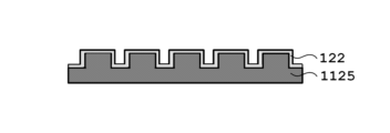
- a silicon wafer is used as a material that can be processed by MEMS, so that an uneven structure for forming the dielectric 122 in an uneven shape can be formed even without the resin body 124 and second conductor 123 as in embodiment 1.
- the third conductor 1125 be made thinner by etching, but an integrated circuit can be formed on the third conductor 1125, enabling integration with a signal processing circuit.
- the dielectric 122 is laminated on the upper surface of the third conductor 1125 ( Figure 8C). Specifically, a film of parylene C is formed on the upper surface of the third conductor 1125 by CVD.
- the first conductor 121 is formed on the surface of the dielectric 122 ( Figure 8D). Specifically, the intermediate body with the dielectric 122 formed is inserted into a specified mold, the mold is evacuated, and then conductive silicone is poured in and hardened. Through this process, a capacitor 1127 consisting of the first conductor 121, the dielectric 122, and the third conductor 1125 is formed, and the manufacture of the bioelectrical signal measurement electrode 1120 is completed.
- the bioelectric signal measurement electrode includes a first conductive part that is in direct contact with the scalp S, which is the skin of a living body, and has flexibility to expand and contract while avoiding foreign objects such as hair H on the skin, a dielectric layered on the first conductive part, and a second conductive part layered on the dielectric, and the first conductive part, the dielectric, and the second conductive part form a capacitor on the scalp S, the first conductive part and the second conductive part are composed of a flat part and a convex part protruding from the surface of the flat part, and the dielectric is formed in an uneven shape between the first conductive part and the second conductive part.
- the first conductive part having such flexibility improves attachment to the human body, and an alternating current of a predetermined frequency flows in the capacitor formed on the scalp S, thereby improving the accuracy of the test.
- the bioelectric signal measurement electrode can reduce the burden on the living body.
- an AC current of a predetermined frequency may be generated in the dielectric.
- the thickness of the dielectric may be 100 nm or more and 1000 nm or less.
- the first conductive portion may be made of a material in which a conductive material is contained in a flexible base material.
- the base material may also be made of a silicone-based resin.
- the conductive material may be biocompatible. This configuration can prevent adverse effects on the living body caused by the bioelectrical signal measurement electrodes, and reduce the burden on the living body.
- the bioelectrical signal measurement electrode may include an external metal terminal laminated on the second conductive portion. This configuration makes it easier to extract the bioelectrical signal measured by the bioelectrical signal measurement electrode.
- the second conductive part and the external metal terminal may be made of a paramagnetic or diamagnetic material.
- the bioelectric signal measuring device includes the bioelectric signal measuring electrode described above, and a processing device connected to the bioelectric signal measuring electrode and transmitting the bioelectric signal received from the bioelectric signal measuring electrode to an external device.
- the bioelectric signal measuring device also improves attachment to the human body due to the flexible first conductive part, and an alternating current of a predetermined frequency flows in the capacitor formed on the scalp S, improving the accuracy of the test.
- the bioelectric signal measuring device can reduce the burden on the living body.
- the manufacturing method of the bioelectric signal measurement electrode is a manufacturing method of the bioelectric signal measurement electrode including a step of laminating a first conductive part having flexibility to extend while avoiding foreign objects such as hair H on the scalp S, a dielectric selected from materials that generate an alternating current of a predetermined frequency when an alternating electric field acts, and a second conductive part sandwiching the dielectric between the first conductive part to form a capacitor, in which the first conductive part and the second conductive part are formed so that a convex part protrudes from the surface of the flat part, and the dielectric is formed in an uneven shape between the first conductive part and the second conductive part.
- the first conductor having flexibility improves attachment to the human body, and an alternating current of a predetermined frequency flows in the capacitor formed on the scalp S, thereby improving the accuracy of the test.
- this manufacturing method makes it possible to provide a bioelectric signal measurement electrode that can reduce the burden on the living body.
- the thickness of the dielectric may be adjusted based on the area of the interface between the first conductor and the dielectric, the dielectric constant of the dielectric, and the strength of the electric field acting on the capacitor. This manufacturing process can increase the voltage generated in the capacitor even in the case of a weak bioelectric signal, thereby improving the detection accuracy of the bioelectric signal itself.
- Bioelectrical signal measuring device 120 1120 Bioelectrical signal measuring electrode 121 First conductor (first conductor portion) 122 Dielectric 123 Second conductor 124 Resin body 125, 1125 Third conductor 126 External metal terminal 127, 1127 Capacitor 130 Processing device
Landscapes
- Life Sciences & Earth Sciences (AREA)
- Health & Medical Sciences (AREA)
- Medical Informatics (AREA)
- Biophysics (AREA)
- Pathology (AREA)
- Engineering & Computer Science (AREA)
- Biomedical Technology (AREA)
- Heart & Thoracic Surgery (AREA)
- Physics & Mathematics (AREA)
- Molecular Biology (AREA)
- Surgery (AREA)
- Animal Behavior & Ethology (AREA)
- General Health & Medical Sciences (AREA)
- Public Health (AREA)
- Veterinary Medicine (AREA)
- Measurement And Recording Of Electrical Phenomena And Electrical Characteristics Of The Living Body (AREA)
Priority Applications (2)
| Application Number | Priority Date | Filing Date | Title |
|---|---|---|---|
| PCT/JP2023/003629 WO2024161641A1 (ja) | 2023-02-03 | 2023-02-03 | 生体電気信号計測電極、生体電気信号計測装置及び生体電気信号計測電極の製造方法 |
| JP2024574224A JPWO2024161641A1 (https=) | 2023-02-03 | 2023-02-03 |
Applications Claiming Priority (1)
| Application Number | Priority Date | Filing Date | Title |
|---|---|---|---|
| PCT/JP2023/003629 WO2024161641A1 (ja) | 2023-02-03 | 2023-02-03 | 生体電気信号計測電極、生体電気信号計測装置及び生体電気信号計測電極の製造方法 |
Publications (1)
| Publication Number | Publication Date |
|---|---|
| WO2024161641A1 true WO2024161641A1 (ja) | 2024-08-08 |
Family
ID=92146229
Family Applications (1)
| Application Number | Title | Priority Date | Filing Date |
|---|---|---|---|
| PCT/JP2023/003629 Ceased WO2024161641A1 (ja) | 2023-02-03 | 2023-02-03 | 生体電気信号計測電極、生体電気信号計測装置及び生体電気信号計測電極の製造方法 |
Country Status (2)
| Country | Link |
|---|---|
| JP (1) | JPWO2024161641A1 (https=) |
| WO (1) | WO2024161641A1 (https=) |
Citations (5)
| Publication number | Priority date | Publication date | Assignee | Title |
|---|---|---|---|---|
| JP2009101032A (ja) * | 2007-10-25 | 2009-05-14 | Fujimura Denshino Gijutsu Kenkyusho:Kk | 遠隔点状3次元電磁波照射システム |
| WO2015180988A1 (en) * | 2014-05-28 | 2015-12-03 | Koninklijke Philips N.V. | Method of manufacturing a flexible conductive track arrangement, flexible conductive track arrangement and neurostimulation system |
| JP2017213391A (ja) * | 2011-11-25 | 2017-12-07 | ヤン,チャンミン | 心拍や電極の接触が良いかどうかを検出するシステム |
| WO2018088400A1 (ja) * | 2016-11-10 | 2018-05-17 | 学校法人 久留米大学 | 脳波スペクトル分析装置のためのセンサ接続装置 |
| JP2018198920A (ja) * | 2017-05-26 | 2018-12-20 | パナソニックIpマネジメント株式会社 | 生体センサおよび生体センサの製造方法 |
-
2023
- 2023-02-03 JP JP2024574224A patent/JPWO2024161641A1/ja active Pending
- 2023-02-03 WO PCT/JP2023/003629 patent/WO2024161641A1/ja not_active Ceased
Patent Citations (5)
| Publication number | Priority date | Publication date | Assignee | Title |
|---|---|---|---|---|
| JP2009101032A (ja) * | 2007-10-25 | 2009-05-14 | Fujimura Denshino Gijutsu Kenkyusho:Kk | 遠隔点状3次元電磁波照射システム |
| JP2017213391A (ja) * | 2011-11-25 | 2017-12-07 | ヤン,チャンミン | 心拍や電極の接触が良いかどうかを検出するシステム |
| WO2015180988A1 (en) * | 2014-05-28 | 2015-12-03 | Koninklijke Philips N.V. | Method of manufacturing a flexible conductive track arrangement, flexible conductive track arrangement and neurostimulation system |
| WO2018088400A1 (ja) * | 2016-11-10 | 2018-05-17 | 学校法人 久留米大学 | 脳波スペクトル分析装置のためのセンサ接続装置 |
| JP2018198920A (ja) * | 2017-05-26 | 2018-12-20 | パナソニックIpマネジメント株式会社 | 生体センサおよび生体センサの製造方法 |
Also Published As
| Publication number | Publication date |
|---|---|
| JPWO2024161641A1 (https=) | 2024-08-08 |
Similar Documents
| Publication | Publication Date | Title |
|---|---|---|
| Yang et al. | Insight into the contact impedance between the electrode and the skin surface for electrophysical recordings | |
| Ferrari et al. | Conducting polymer tattoo electrodes in clinical electro-and magneto-encephalography | |
| Kim et al. | Skin preparation–free, stretchable microneedle adhesive patches for reliable electrophysiological sensing and exoskeleton robot control | |
| Chen et al. | Flexible inorganic bioelectronics | |
| Ji et al. | Skin-integrated, biocompatible, and stretchable silicon microneedle electrode for long-term EMG monitoring in motion scenario | |
| Tian et al. | Large-area MRI-compatible epidermal electronic interfaces for prosthetic control and cognitive monitoring | |
| Srivastava et al. | Long term biopotential recording by body conformable photolithography fabricated low cost polymeric microneedle arrays | |
| Lee et al. | Self-adhesive and capacitive carbon nanotube-based electrode to record electroencephalograph signals from the hairy scalp | |
| Jeong et al. | Solderable and electroplatable flexible electronic circuit on a porous stretchable elastomer | |
| TWI481383B (zh) | 生醫感測器及其電極結構 | |
| Viventi et al. | Flexible, foldable, actively multiplexed, high-density electrode array for mapping brain activity in vivo | |
| Lee et al. | Characterization of Ag/AgCl dry electrodes for wearable electrophysiological sensing | |
| US8892198B2 (en) | Devices and methods for evaluating tissue | |
| CN113180604B (zh) | 用于颅内生理生化信息获取的多模态传感器制备方法 | |
| CN104473637B (zh) | 用于脑电信号探测的电极探针及应用其的干电极单元 | |
| CN113197548A (zh) | 颅内植入式柔性多模态生理生化信息监测设备 | |
| CN108553102A (zh) | 一种柔性可拉伸多通道凸形表面肌电极及其制备方法 | |
| Márton et al. | A multimodal, SU-8-Platinum-Polyimide microelectrode array for chronic in vivo neurophysiology | |
| US9144387B2 (en) | Electrode for measuring bio potential, method of manufacturing the electrode, and system for measuring physiological signal | |
| JP2004504877A (ja) | 非侵入神経の位置と画像装置のための電極配列とセンサー装着システム | |
| Vasconcelos et al. | The arch electrode: A novel dry electrode concept for improved wearing comfort | |
| Kim et al. | Emerging bio‐interfacing wearable devices for signal monitoring: overview of the mechanisms and diverse sensor designs to target distinct physiological bio‐parameters | |
| CN113867006B (zh) | 一种基于γ-Fe2O3@NiO磁性氧化物纳米片的柔性多功能角膜接触镜 | |
| KR101843083B1 (ko) | 다중의 단위 측정기들을 포함하는 생체 신호 측정 장치 및 방법 | |
| Xiong et al. | Sustainable development of electroencephalography materials and technology |
Legal Events
| Date | Code | Title | Description |
|---|---|---|---|
| 121 | Ep: the epo has been informed by wipo that ep was designated in this application |
Ref document number: 23919778 Country of ref document: EP Kind code of ref document: A1 |
|
| ENP | Entry into the national phase |
Ref document number: 2024574224 Country of ref document: JP Kind code of ref document: A |
|
| WWE | Wipo information: entry into national phase |
Ref document number: 2024574224 Country of ref document: JP |
|
| NENP | Non-entry into the national phase |
Ref country code: DE |
|
| 32PN | Ep: public notification in the ep bulletin as address of the adressee cannot be established |
Free format text: NOTING OF LOSS OF RIGHTS PURSUANT TO RULE 112(1) EPC (EPO FORM 1205A DATED 28.10.2025) |