WO2024157969A1 - 半導体素子の製造方法 - Google Patents
半導体素子の製造方法 Download PDFInfo
- Publication number
- WO2024157969A1 WO2024157969A1 PCT/JP2024/001836 JP2024001836W WO2024157969A1 WO 2024157969 A1 WO2024157969 A1 WO 2024157969A1 JP 2024001836 W JP2024001836 W JP 2024001836W WO 2024157969 A1 WO2024157969 A1 WO 2024157969A1
- Authority
- WO
- WIPO (PCT)
- Prior art keywords
- semiconductor wafer
- semiconductor
- cutting
- cutting lines
- manufacturing
- Prior art date
- Legal status (The legal status is an assumption and is not a legal conclusion. Google has not performed a legal analysis and makes no representation as to the accuracy of the status listed.)
- Ceased
Links
Images




Classifications
-
- H—ELECTRICITY
- H10—SEMICONDUCTOR DEVICES; ELECTRIC SOLID-STATE DEVICES NOT OTHERWISE PROVIDED FOR
- H10P—GENERIC PROCESSES OR APPARATUS FOR THE MANUFACTURE OR TREATMENT OF DEVICES COVERED BY CLASS H10
- H10P95/00—Generic processes or apparatus for manufacture or treatments not covered by the other groups of this subclass
Definitions
- This disclosure relates to a method for manufacturing semiconductor devices.
- the objective of this disclosure is to provide a method for manufacturing semiconductor elements that can suppress deviations in the cut line.
- One embodiment of the present disclosure includes a process for preparing a semiconductor wafer after wafer processing, the semiconductor wafer including a SiC semiconductor substrate having a first main surface on one side and a second main surface on the other side, with a plurality of element formation regions and a planned cutting line that divides the plurality of element formation regions, and a semiconductor element structure formed in each of the element formation regions; a wafer holding process for holding the semiconductor wafer on a dicing tape by adhering the dicing tape to the surface of the first main surface side of the semiconductor wafer; and a dicing process for cutting the semiconductor wafer from the surface of the second main surface side of the semiconductor wafer along the planned cutting line with a dicing blade, the direction along the first main surface and perpendicular to the orientation flat of the SiC semiconductor substrate being defined as a first direction, and the direction along the first main surface and parallel to the orientation flat being defined as a second direction.
- the method includes a plurality of first cutting lines that are parallel to the first direction and spaced apart in the second direction, and a plurality of second cutting lines that are parallel to the second direction and spaced apart in the first direction and intersect with the first cutting lines
- the dicing process includes a first process of cutting the semiconductor wafer along a first center line that is a first cutting line that passes through a portion closest to the center of the SiC semiconductor substrate among the plurality of first cutting lines, and a second process of cutting the semiconductor wafer along a second center line that is a second cutting line that passes through a portion closest to the center of the SiC semiconductor substrate among the plurality of second cutting lines, after the first process, and a second process of cutting the semiconductor wafer along each of the plurality of cutting lines excluding the first center line and the second center line.
- This manufacturing method can prevent the cut line from shifting.
- FIG. 1 is a schematic plan view of a semiconductor wafer after a wafer process used in a method for manufacturing a semiconductor device according to an embodiment of the present disclosure.
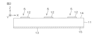
- FIG. 2 is a cross-sectional view taken along line II-II in FIG.
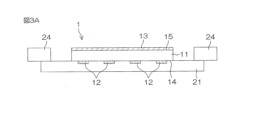
- FIG. 3A is a cross-sectional view for explaining a part of a process for manufacturing a semiconductor element assembly for shipment from a semiconductor wafer after the wafer process.
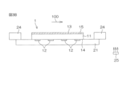
- FIG. 3B is a cross-sectional view for explaining the step subsequent to that of FIG. 3A.
- FIG. 3C is a plan view for explaining the step subsequent to that of FIG. 3A.
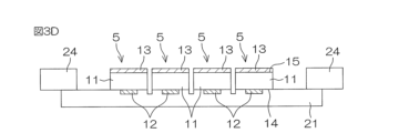
- FIG. 3D is a cross-sectional view for explaining the next step after FIGS. 3B and 3C.
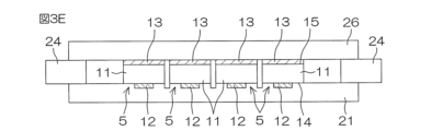
- FIG. 3E is a cross-sectional view for explaining the step subsequent to FIG. 3D.
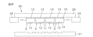
- FIG. 3F is a cross-sectional view for explaining the step subsequent to FIG. 3E.
- FIG. 4 is a schematic cross-sectional view for explaining the structure of the dicing tape.
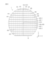
- FIG. 5A is a plan view for explaining a part of the dicing step of FIG. 3D.
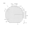
- FIG. 5B is a plan view for explaining the step subsequent to that of FIG. 5A.
- FIG. 5C is a plan view for explaining the step subsequent to FIG. 5B.
- FIG. 5D is a plan view for explaining the step subsequent to FIG. 5C.
- FIG. 1 is a schematic plan view of a semiconductor wafer 1 after a wafer process used in a method for manufacturing a semiconductor device according to one embodiment of the present disclosure.
- the semiconductor wafer 1 is, for example, a SiC (silicon carbide) semiconductor wafer including a SiC single crystal.
- the SiC single crystal is a hexagonal SiC single crystal.
- the SiC single crystal may be a 4H-SiC single crystal.
- the unit cell of the 4H-SiC single crystal includes a tetrahedral structure in which one Si atom is bonded to four C atoms in a tetrahedral arrangement (regular tetrahedral arrangement).
- the unit cell has an atomic arrangement in which the tetrahedral structures are stacked in four periods.
- the unit cell has a hexagonal prism structure with a regular hexagonal silicon face, a regular hexagonal carbon face, and six side faces connecting the silicon face and the carbon face.
- the silicon face is a terminal face terminated by Si atoms.
- Si atom is located at each of the six vertices of the regular hexagon, and one Si atom is located at the center of the regular hexagon.
- the carbon face is a terminal face terminated by C atoms.
- one C atom is located at each of the six vertices of the regular hexagon, and one C atom is located at the center of the regular hexagon.
- the semiconductor wafer 1 includes a plurality of element formation regions 2 and scribe regions (dicing streets) 3 that partition the plurality of element formation regions 2.
- each element formation region 2 is rectangular.
- the plurality of element formation regions 2 are aligned in a matrix at intervals in the X direction (horizontal direction) and Y direction (vertical direction) shown in FIG. 1.
- Planned cutting lines 4 are set in the scribe region 3 of the semiconductor wafer 1.
- a semiconductor element 5 is formed in each element formation region 2.
- the semiconductor element 5 is, for example, a vertical power semiconductor element.
- the semiconductor element 5 is a vertical diode or a vertical transistor.
- the vertical diode may include a vertical SBD (Schottky Barrier Diode).
- the vertical transistor may include a vertical MISFET (Metal Insulator Semiconductor Field Effect Transistor).
- Figure 2 is a cross-sectional view taken along line II-II in Figure 1.
- the semiconductor wafer 1 includes a semiconductor substrate 11, a first electrode 12, and a second electrode 13.
- the Z direction shown in FIG. 1 and FIG. 2 indicates the thickness direction of the semiconductor substrate 1.
- the semiconductor substrate 11 is, for example, a SiC substrate including a SiC single crystal.
- the SiC single crystal is a hexagonal SiC single crystal.
- the semiconductor substrate 11 has a first main surface 14 and a second main surface 15 opposite to the first main surface. It is preferable that the first main surface 14 is a (0001) surface (silicon surface) and the second main surface 15 is a (000-1) surface (carbon surface). This configuration is effective when the semiconductor element includes a SiC-MOSFET or a SiC-SBD.
- the thickness of the semiconductor substrate 11 is preferably 80 ⁇ m or more and 350 ⁇ m or less.
- the first electrode 12 is a metal electrode formed for each element formation region 2 (each semiconductor element 5) on the first main surface 14 of the semiconductor substrate 11. In this embodiment, the first electrode 12 is formed in the center of the first main surface 14 of each element formation region 2.
- the second electrode 13 is a metal electrode formed uniformly on the second main surface 15 of the semiconductor substrate 11. That is, the second electrode 13 is formed in common to a plurality of element formation regions 2 in the semiconductor wafer 1.
- the second electrode 13 may cover the entire second main surface 15.
- the second electrode 13 is formed, for example, from a laminated film of titanium (Ti), nickel (Ni), palladium (Pd), and gold (Au).
- the second electrode 13 may be formed from other materials such as aluminum, copper, silver, titanium nitride, or tungsten.
- the second electrode 13 preferably has a single layer structure or a multilayer structure including at least one of a Ti layer, a Ni layer, a Ni alloy layer, and an Au layer. It is particularly preferable that the second electrode 13 has a single layer structure or a multilayer structure including either or both of a Ni layer and a Ni alloy layer.
- the second electrode 13 may have a multilayer structure including a Ti layer, a Ni layer, and an Au layer stacked in this order from the second main surface 15 side.
- the second electrode 13 may have a layered structure including a NiSi layer, a Ti layer, and a Ni layer stacked in this order from the second main surface 15 side.
- the second electrode 13 may have a layered structure including a Ni layer, a Ti layer, and a Ni layer stacked in this order from the second main surface 15 side.
- the second electrode 13 may have a layered structure including a Ni layer, a Ti layer, and a NiV layer stacked in this order from the second main surface 15 side.
- the second electrode 13 may have a layered structure including a Ni layer and an Au layer stacked in this order from the second main surface 15 side.
- the thickness of the second electrode 13 may be 500 nm or more.
- the thickness of the second electrode 13 may be 1500 nm or less.
- the second electrode 13 may be configured so that the total layer thickness of the Ni layers or Ni alloy layers in the laminate structure is 500 nm or more.
- the second electrode 13 may be configured so that the Ni layers alone in the laminate structure are 500 nm or more.
- the second electrode 13 may be configured so that the Ti layer is 50 nm or more and 100 nm or less.
- a semiconductor element having two electrodes e.g., a diode
- a semiconductor element having three or more electrodes e.g., a transistor
- one semiconductor element in the semiconductor wafer 1 has two or more first electrodes 12 formed on the first main surface 14.
- the configuration of the semiconductor wafer 1, the configuration of the semiconductor element 5, and the manufacturing method thereof are publicly known configurations and manufacturing methods.
- a semiconductor substrate 11 made of SiC is prepared.
- the semiconductor substrate 11 may have a configuration in which a semiconductor layer having a lower impurity concentration than a semiconductor substrate having a relatively high impurity concentration is formed on the semiconductor substrate by epitaxial growth.
- an internal structure (semiconductor element structure) corresponding to the semiconductor element is formed on the surface layer of the semiconductor substrate 11.
- a plurality of first electrodes 12 are formed on the first main surface 14 of the semiconductor substrate 11.
- a second electrode 13 is formed on the second main surface 15 of the semiconductor substrate 11. The second electrode 13 is formed over the entire area of the second main surface 15 (the entire surface of the semiconductor wafer 1).
- the entire area of the second main surface 15 (the entire surface of the semiconductor wafer 1) does not necessarily have to be the entire second main surface 15, and also includes cases where the second electrode 13 is not formed in some areas, such as the peripheral part of the semiconductor wafer 1.
- the semiconductor substrate 11 may be adjusted to a predetermined thickness by a grinding method or the like before the process of forming the second electrode 13.
- the surface on the first main surface 14 side of the semiconductor wafer 1 is an uneven surface.
- the second electrode 13 is formed over the entire area of the second main surface 15 of the semiconductor substrate 11, the surface on the second main surface 15 side of the semiconductor wafer 1 is a flat surface.
- a backside structure such as a collector layer is formed on the surface layer of the second main surface 15 before the process of forming the second electrode 13.
- the semiconductor wafer 1 is cut (diced) by a dicing blade along the intended cutting lines 4. This divides the semiconductor wafer 1 into a plurality of semiconductor elements (chips) 5, each including an element formation region 2.
- the dicing direction may be the positive or negative direction of the X-axis and Y-axis.
- the X direction is a direction parallel to the orientation flat 6 of the semiconductor wafer 1
- the Y direction is a direction along the first main surface 14 of the semiconductor wafer 1 and perpendicular to the orientation flat 6.
- the X direction is the [1-100] direction of the SiC single crystal
- the Y direction is the [11-20] direction of the SiC single crystal.
- the planned cutting lines 4 include a plurality of first planned cutting lines 4A extending in the [11-20] direction (Y direction) and a plurality of second planned cutting lines 4B extending along the [1-100] direction (X direction).
- Figures 3A to 3F are cross-sectional views illustrating an example of a process for manufacturing a semiconductor element assembly for shipment from a semiconductor wafer 1 after wafer processing.
- the semiconductor wafer 1 including the semiconductor substrate 11, the first electrode 12, and the second electrode 13 is held (supported) by the dicing tape 21. That is, the semiconductor wafer 1 is fixed to the ring frame 24 by the dicing tape 21.
- the dicing tape 21 is attached to the surface of the semiconductor wafer 1 on the first main surface 14 side with the surface of the semiconductor wafer 1 on the second main surface 15 side facing up, thereby holding the semiconductor wafer 1 by the dicing tape 21.
- the dicing tape 21 is applied to the uneven surface that is the surface on the first main surface 14 side of the semiconductor wafer 1.
- the semiconductor wafer 1 is held by the dicing tape 21 in a position that is upside down from the position shown in FIG. 2.
- the dicing tape 21 includes a substrate (dicing tape body) 22 and an adhesive layer 23 formed on one side of the substrate 22.
- the substrate 22 includes, for example, polyethylene terephthalate or polyolefin.
- the thickness of the substrate 22 is preferably 50 ⁇ m or more and 300 ⁇ m or less.
- the adhesive layer 23 contains an adhesive that hardens when exposed to ultraviolet light.
- the dicing tape 21 is applied to the uneven surface that is the surface on the first main surface 14 side of the semiconductor wafer 1, so it is necessary for the adhesive layer 23 to have step adhesion properties.
- the thickness of the adhesive layer 23 is made thicker than that of an adhesive layer of a normal dicing tape that is applied to a flat surface.
- the thickness of the adhesive layer 23 is preferably 30 ⁇ m or more and 100 ⁇ m or less.
- the adhesive of the dicing tape 21 is semi-cured by irradiating the dicing tape 21 with ultraviolet light (semi-curing process).
- the thickness of the adhesive layer 23 is thicker than that of an ordinary dicing tape that is applied to a flat surface.
- the adhesive is soft, there is a risk that the semiconductor element (chip) 5 may shake during dicing, which will be described later. Therefore, in order to reduce the shaking of the semiconductor element 5 during dicing, the adhesive of the dicing tape 21 is semi-cured.
- the semiconductor wafer 1 is moved in the direction of the arrow 100 together with the dicing tape 21.
- multiple LED lights 25 are arranged at intervals in a direction that runs along the surface of the dicing tape 21 and is perpendicular to the direction of the arrow 100.
- ultraviolet light emitted from the LED lights 25 is irradiated onto the dicing tape 21.
- the ultraviolet irradiation energy for semi-curing the adhesive of the dicing tape 21 is preferably 20 mJ/cm 2 or more and 500 mJ/cm 2 or less, and more preferably 20 mJ/cm 2 or more and 200 mJ/cm 2 or less.
- ultraviolet rays may be irradiated from below the semiconductor wafer 1 by a mercury lamp (not shown) for a certain period of time onto at least the entire area of the dicing tape 21 that faces the semiconductor wafer 1.
- a mercury lamp not shown
- the preferred range of ultraviolet irradiation energy for semi-curing the adhesive of the dicing tape 21 is the same as the range described above.
- a dicing process is performed. That is, as shown in FIG. 3D, the semiconductor wafer 1 is cut along the intended cutting lines 4 from the surface of the semiconductor wafer 1 on the second main surface 15 side by a dicing blade (not shown). This divides the semiconductor wafer 1 into a plurality of semiconductor elements (chips) 5. A detailed description of the dicing process will be given later.
- an element holding tape (shipping tape) 26 for holding multiple semiconductor elements (chips) 5 is attached to the surface of the semiconductor wafer 1 on the second main surface 15 side. Specifically, the semiconductor wafer 1 is fixed to the ring frame 24 by the element holding tape 26.
- the adhesive strength of the element holding tape 26 is stronger than that of the dicing tape 21. Therefore, after the element holding tape 26 is attached to the surface on the second main surface 15 side of the semiconductor wafer 1, as shown in FIG. 3F, the dicing tape 21 is peeled off from each semiconductor element (chip) 5, and each semiconductor element 5 is held by the element holding tape 26. In this way, a semiconductor element assembly 30 for shipment is manufactured.
- each semiconductor element (chip) 5 is peeled off from the element holding tape 26. In this way, individual semiconductor elements (chips) 5 are obtained.
- FIGS. 5A to 5D are plan views for explaining an example of detailed steps of the dicing process of FIG. 3D.
- FIG. 5 omits the configuration of the semiconductor wafer 1 other than the intended cutting lines 4 (4A, 4B).
- the dicing device has the ability to cut two lines simultaneously using two dicing blades.
- the planned cutting lines 4 (4A, 4B) shown by solid lines indicate the planned cutting lines 4 (4A, 4B) that have already been cut in the current process or an earlier process.
- the planned cutting lines 4 (4A, 4B) shown by dashed lines indicate the planned cutting lines 4 (4A, 4B) that have not been cut at the end of the process.
- the semiconductor wafer 1 is cut along the first planned cutting line 4A (hereinafter referred to as the "first center line 4Ac") that passes through the point closest to the center 200 of the semiconductor substrate 11 among the multiple first planned cutting lines 4A.
- the center 200 of the semiconductor substrate 11 refers to the center of the semiconductor substrate on the disk before the orientation flat 6 is formed.
- the semiconductor wafer 1 is cut along the second cutting line 4B (hereinafter referred to as the "second center line 4Bc") that passes through the point closest to the center of the semiconductor substrate 11 among the multiple second cutting lines 4B.
- the semiconductor wafer 1 is cut along each of the second cutting lines 4B, except for the second center line 4Bc.
- the semiconductor wafer 1 is cut along the two second planned cutting lines 4B-1 that are adjacent to the outside of the second center line 4Bc.
- the semiconductor wafer 1 is cut along the two second planned cutting lines 4B-2 that are adjacent to the outside of the two second planned cutting lines 4B-1 that were previously cut.
- the semiconductor wafer 1 is cut in a similar manner along the remaining second planned cutting lines 4B.
- the semiconductor wafer 1 is cut along each of the first cutting lines 4A, except for the first center line 4Ac.
- the semiconductor wafer 1 is cut along two first planned cutting lines 4A-1 that are adjacent to the outside of the first center line 4Ac.
- the semiconductor wafer 1 is cut along two first planned cutting lines 4A-2 that are adjacent to the outside of the two first planned cutting lines 4A-1 that were previously cut.
- the semiconductor wafer 1 is cut in a similar manner along the remaining first planned cutting lines 4A. In this manner, the semiconductor wafer 1 is divided into a plurality of semiconductor elements (chips) 5.
- the step in FIG. 5D may be performed before the step in FIG. 5C.
- the step in FIG. 5D may be performed after the step in FIG. 5B
- the step in FIG. 5C may be performed after the step in FIG. 5D.
- the step in FIG. 5B may be performed before the step in FIG. 5A. That is, the step in FIG. 5B may be performed first, and then the step in FIG. 5A may be performed after the step in FIG. 5B.
- the step in FIG. 5D may be performed after the step in FIG. 5A, and then the step in FIG. 5C may be performed after the step in FIG. 5D.
- the step in FIG. 5C may be performed after the step in FIG. 5A, and then the step in FIG. 5D may be performed after the step in FIG. 5C.
- the dicing process is performed from the surface on the second main surface 15 side of the semiconductor wafer 1. This makes it possible to smooth the cut surface and suppress the occurrence of chipping, compared to when dicing is performed from the surface on the first main surface 14 side of the semiconductor wafer 1.
- the dicing tape 21 is applied to the uneven surface that is the surface on the first main surface 14 side of the semiconductor wafer 1, so the dicing tape 21 needs to have step absorption properties compared to when the dicing tape is applied to the flat surface that is the surface on the second main surface 15 side of the semiconductor wafer 1.
- the adhesive layer 23 of the dicing tape 21 is made thicker than the adhesive layer of a normal dicing tape that is applied to a flat surface. If the adhesive layer 23 of the dicing tape 21 is made thicker, the adhesive will be soft and there is a risk that the semiconductor element (chip) 5 will shake during dicing, inducing chipping.
- the adhesive of the dicing tape 21 is semi-cured by irradiating the dicing tape 21 with ultraviolet light before dicing. This reduces the shaking of the semiconductor element (chip) 5 during dicing, thereby suppressing the occurrence of chipping.
- the semiconductor wafer 1 Since the semiconductor wafer 1 is warped, the semiconductor wafer 1 has stress toward the center 200 of the semiconductor substrate 11. For this reason, if dicing is performed while the semiconductor wafer 1 still has warpage, the dicing blade may meander or move diagonally relative to the intended cutting line 4. In particular, when a glass chuck table is used to ensure visibility, suction is performed via grooves, but sufficient suction is not ensured over the entire surface, so the cut line is likely to shift relative to the intended cutting line 4 at the cutout portion.
- the semiconductor wafer 1 in the dicing process, is first cut along the first planned cutting line 4A (first center line 4Ac) that passes through the location closest to the center 200 of the semiconductor substrate 11 among the multiple first planned cutting lines 4A (hereinafter referred to as "Process A").
- the semiconductor wafer 1 is cut along the second planned cutting line 4B (second center line 4Bc) that passes through the location closest to the center 200 of the semiconductor substrate 11 among the multiple second planned cutting lines 4B (hereinafter referred to as "Process B").
- Process B is performed first, and then Process A is performed.
- the semiconductor wafer 1 is cut along each of the remaining cutting lines 4 out of the multiple cutting lines 4.
- the semiconductor wafer 1 has stress directed toward the center 200 of the semiconductor substrate 11.
- stress acts perpendicular to the cutting direction, so misalignment of the cut line is less likely to occur compared to when cutting the peripheral portion of the semiconductor wafer 1 in the X direction. Therefore, when cutting the semiconductor wafer 1 by process A, misalignment of the cut line is less likely to occur.
- the semiconductor wafer 1 is cut along each of the remaining planned cutting lines 4, so that the cut lines are less likely to shift when cutting along each of the remaining planned cutting lines 4. This makes it possible to prevent the dicing blade from meandering or moving diagonally relative to the planned cutting lines.
- the order of cutting in the cutting process carried out after process A and process B may be different from the order described above.
- the adhesive on the dicing tape 21 is semi-cured by irradiating it with ultraviolet light before dicing, but this semi-curing step may be omitted.
- the method includes the steps of: preparing a semiconductor wafer (1) after a wafer process, the semiconductor wafer (1) including a SiC semiconductor substrate (11) having a first main surface (14) on one side and a second main surface (15) on the other side, and including a plurality of element formation regions (2) and a cutting line (4) that divides the plurality of element formation regions (2), and a semiconductor element structure formed in each of the element formation regions (2); a wafer holding step of holding the semiconductor wafer (1) on the dicing tape (21) by attaching the dicing tape (21) to a surface of the semiconductor wafer (1) on the first main surface side; and a dicing step of cutting the semiconductor wafer (1) along the cutting line (4) from the surface of the semiconductor wafer (1) on the second main surface side by a dicing blade,
- a direction along the first main surface (14) and perpendicular to an orientation flat (6) of the SiC semiconductor substrate (11) is defined as a first direction (Y direction), and a direction along the first main surface (1
- [Appendix 1-2] The method for manufacturing a semiconductor element according to [Appendix 1-1], wherein the thickness of the SiC semiconductor substrate (11) is 80 ⁇ m or more and 350 ⁇ m or less.
- the SiC semiconductor substrate (11) is a SiC semiconductor substrate including a hexagonal SiC single crystal, the first direction is a [11-20] direction, The method for manufacturing a semiconductor element according to [Appendix 1-1] or [Appendix 1-2], wherein the second direction is a [1-100] direction.
- the second step comprises: a C step of cutting the semiconductor wafer (1) along each of the second cutting lines (4B) except for the second center line (4Bc) among the plurality of second cutting lines (4B);
- the method for manufacturing a semiconductor element described in [Appendix 1-4] includes, after the step C, a step D of cutting the semiconductor wafer (1) along each of the plurality of first cutting lines (4A) except for the first central line (4Ac) among the plurality of first cutting lines (4A).
- the second step comprises: a step E of cutting the semiconductor wafer (1) along each of the first cutting lines (4A) except for the first center line (4Ac) among the plurality of first cutting lines (4A);
- the method for manufacturing a semiconductor element described in [Appendix 1-4] includes, after the step E, a step F of cutting the semiconductor wafer (1) along each of the plurality of second cutting lines (4B) except for the second center line (4Bc) among the plurality of second cutting lines (4B).
- the second step comprises: a G step of cutting the semiconductor wafer (1) along each of the first cutting lines (4A) except for the first center line (4Ac) among the plurality of first cutting lines (4A);
- the method for manufacturing a semiconductor element described in [Appendix 1-7] includes, after the G step, an H step of cutting the semiconductor wafer (1) along each of the second cutting lines (4B) among the plurality of second cutting lines (4B) except for the second center line (4Bc).
- the second step comprises: a step I of cutting the semiconductor wafer (1) along each of the second cutting lines (4B) except for the second center line (4Bc) among the plurality of second cutting lines (4B);
- the method for manufacturing a semiconductor element described in [Appendix 1-7] includes, after the step I, a step J of cutting the semiconductor wafer (1) along each of the plurality of first cutting lines (4A) except for the first central line (4Ac) among the plurality of first cutting lines (4A).
- the semiconductor wafer (1) includes a first electrode (12) formed on the first main surface for each of the element formation regions, and a second electrode (13) formed over the entire surface of the second main surface (15).
- the dicing tape (21) has an adhesive that hardens when exposed to ultraviolet light, The method for manufacturing a semiconductor device according to [Appendix 1-10], further comprising a step of semi-curing the adhesive by irradiating the dicing tape (21) with ultraviolet light between the wafer holding step and the dicing step.
- [Appendix 1-12] a bonding step of bonding an element holding tape (26) to the second main surface side of the semiconductor wafer (1) after the dicing step;
- the dicing tape (21) includes a substrate (22) and an adhesive layer (23) made of the adhesive formed on one surface of the substrate (22), The method for producing a semiconductor element according to [Appendix 1-11], wherein the thickness of the pressure-sensitive adhesive layer (23) is 30 ⁇ m or more and 100 ⁇ m or less.
- the substrate (22) comprises polyethylene terephthalate or polyolefin;
- [Appendix 1-15] The method for manufacturing a semiconductor element according to any one of [Appendix 1-11] to [Appendix 1-13], wherein the ultraviolet irradiation energy in the step of semi-curing the adhesive is 50 mJ/ cm2 or more and 500 mJ/ cm2 or less.
- [Appendix 1-16] The method for manufacturing a semiconductor element according to any one of [Appendix 1-11] to [Appendix 1-13], wherein the ultraviolet irradiation energy in the step of semi-curing the adhesive is 50 mJ/ cm2 or more and 200 mJ/ cm2 or less.
- [Appendix 1-18] The method for manufacturing a semiconductor element according to any one of [Appendix 1-11] to [Appendix 1-16], wherein in the step of semi-curing the adhesive, ultraviolet light is irradiated from below the semiconductor wafer (1) by a mercury lamp for a certain period of time onto at least the entire area of the dicing tape (21) that faces the semiconductor wafer (1).
Landscapes
- Dicing (AREA)
Abstract
ダイシング工程は、複数の第1切断予定ラインのうち、SiC半導体基板の中心に最も近い箇所を通る第1切断予定ラインである第1中央ラインに沿って半導体ウエハを切断するA工程と、複数の第2切断予定ラインのうち、SiC半導体基板の中心に最も近い箇所を通る第2切断予定ラインである第2中央ライン沿って半導体ウエハを切断するB工程とを行う第1工程と、第1工程の後、複数の切断予定ラインのうち、第1中央ラインおよび第2中央ラインを除いた各切断予定ラインに沿って半導体ウエハを切断する第2工程とを含む。
Description
この出願は、2023年1月27日に日本国特許庁に提出された特許出願2023-010594号に基づく優先権を主張しており、この出願の全内容はここに引用により組み込まれるものとする。
本開示は、半導体素子の製造方法に関する。
半導体素子の製造方法では、ダイシングブレードを用いて半導体ウエハをチップ単位に分割する工程が実施されることがある(たとえば、特許文献1参照)。
本開示の目的は、カットラインのずれを抑制できる半導体素子の製造方法を提供することである。
本開示の一実施形態は、一方側の第1主面および他方側の第2主面を有し、複数の素子形成領域および前記複数の素子形成領域を区画する切断予定ラインが設定されたSiC半導体基板と、前記各素子形成領域に形成された半導体素子構造とを含む、ウエハプロセス後の半導体ウエハを用意する工程と、前記半導体ウエハの前記第1主面側の表面に、ダイシングテープを貼着することにより、前記半導体ウエハを前記ダイシングテープに保持させるウエハ保持工程と、ダイシングブレードによって、前記半導体ウエハの前記第2主面側の表面から、前記切断予定ラインに沿って前記半導体ウエハを切断するダイシング工程とを含み、前記第1主面に沿う方向でかつ前記SiC半導体基板のオリエンテーション・フラットに直交する方向を第1方向とし、前記第1主面に沿う方向でかつ前記オリエンテーション・フラットに平行な方向を第2方向とすると、前記切断予定ラインは、前記第1方向に平行でかつ前記第2方向に間隔を空けて配置された複数の第1切断予定ラインと、前記第2方向に平行でかつ前記第1方向に間隔を空けて配置され、前記第1切断予定ラインと交差する複数の第2切断予定ラインとを含み、前記ダイシング工程は、前記複数の第1切断予定ラインのうち、前記SiC半導体基板の中心に最も近い箇所を通る第1切断予定ラインである第1中央ラインに沿って前記半導体ウエハを切断するA工程と、前記複数の第2切断予定ラインのうち、前記SiC半導体基板の中心に最も近い箇所を通る第2切断予定ラインである第2中央ラインに沿って前記半導体ウエハを切断するB工程とを行う第1工程と、前記第1工程の後、前記複数の切断予定ラインのうち、前記第1中央ラインおよび前記第2中央ラインを除いた各切断予定ラインに沿って前記半導体ウエハを切断する第2工程とを含む、半導体素子の製造方法を提供する。
この製造方法では、カットラインのずれを抑制できる。
上述のまたはさらに他の目的、特徴および効果は、添付図面を参照して次に述べる実施形態の説明により明らかにされる。
以下では、添付図面を参照して、本開示の実施形態を詳細に説明する。
図1は、本開示の一実施形態に係る半導体装置の製造方法に用いられるウエハプロセス後の半導体ウエハ1の図解的な平面図である。
半導体ウエハ1は、たとえば、SiC単結晶を含むSiC(炭化珪素)半導体ウエハである。SiC単結晶は、この実施形態では、六方晶SiC単結晶である。SiC単結晶は、4H-SiC単結晶であってもよい。4H-SiC単結晶の単位セルは、1つのSi原子に対して4つのC原子が四面体配列(正四面体配列)の関係で結合された四面体構造を含む。単位セルは、四面体構造が4周期積層された原子配列を有している。
単位セルは、正六角形のシリコン面、正六角形のカーボン面、ならびに、シリコン面およびカーボン面を接続する6つの側面を有する六角柱構造を有している。シリコン面は、Si原子によって終端された終端面である。シリコン面では、正六角形の6つの頂点に1つのSi原子がそれぞれ位置し、正六角形の中心に1つのSi原子が位置している。カーボン面は、C原子によって終端された終端面である。カーボン面では、正六角形の6つの頂点に1つのC原子がそれぞれ位置し、正六角形の中心に1つのC原子が位置している。
半導体ウエハ1は、複数の素子形成領域2および複数の素子形成領域2を区画するスクライブ領域(ダイシングストリート)3を含む。図1に示す平面視において、各素子形成領域2は矩形状である。図1に示す平面視において、複数の素子形成領域2は、図1に示されるX方向(横方向)およびY方向(縦方向)に間隔をおいて行列状に整列して配置されている。
隣接する素子形成領域2の間の部分がスクライブ領域3である。半導体ウエハ1のスクライブ領域3に、切断予定ライン4が設定されている。
各素子形成領域2には、半導体素子5が形成されている。半導体素子5は、たとえば、縦型パワー半導体素子である。具体的には、半導体素子5は、縦型ダイオードまたは縦型トランジスタである。縦型ダイオードは、縦型SBD(Schottky Barrier Diode)を含んでいてもよい。縦型トランジスタは、縦型MISFET(Metal Insulator Semiconductor Field Effect Transistor)を含んでいてもよい。
図2は、図1のII-II線に沿う断面図である。
図2に示されるように、半導体ウエハ1は、半導体基板11、第1電極12および第2電極13を含む。図1および図2に示されるZ方向は、半導体基板1の厚さ方向を示している。
半導体基板11は、たとえば、SiC単結晶を含むSiC基板である。SiC単結晶は、この実施形態では、六方晶SiC単結晶である。半導体基板11は、第1主面14および第1主面とは反対側の第2主面15を有する。第1主面14が(0001)面(シリコン面)であり、第2主面15は(000-1)面(カーボン面)であることが好ましい。このような構成は、半導体素子がSiC-MOSFETやSiC-SBDを含む場合に有効である。半導体基板11の厚さは、80μm以上350μm以下であることが好ましい。
第1電極12は、半導体基板11の第1主面14上に、素子形成領域2毎(半導体素子5毎)に形成されている金属電極である。この実施形態では、第1電極12は、各素子形成領域2の第1主面14の中央部に形成されている。
第2電極13は、半導体基板11の第2主面15上に一様に形成されている金属電極である。つまり、第2電極13は、半導体ウエハ1においては、複数の素子形成領域2に共通に形成されている。第2電極13は、第2主面15の全域を被覆していてもよい。第2電極13は、たとえば、チタン(Ti)、ニッケル(Ni)、パラジウム(Pd)、金(Au)の積層膜によって形成される。むろん、第2電極13は、アルミニウム、銅、銀、窒化チタンまたはタングステンなどの他の材料によって形成されてもよい。
第2電極13は、Ti層、Ni層、Ni合金層およびAu層のうちの少なくとも1つを含む単層構造または積層構造を有していることが好ましい。第2電極13は、Ni層およびNi合金層のいずれか一方または双方を含む単層構造または積層構造を有していることが特に好ましい。たとえば、第2電極13は、第2主面15側からこの順に積層されたTi層、Ni層およびAu層を含む積層構造を有していてもよい。
第2電極13は、第2主面15側からこの順に積層されたNiSi層、Ti層およびNi層を含む積層構造を有していてもよい。第2電極13は、第2主面15側からこの順に積層されたNi層、Ti層およびNi層を含む積層構造を有していてもよい。第2電極13は、第2主面15側からこの順に積層されたNi層、Ti層およびNiV層を含む積層構造を有していてもよい。第2電極13は、第2主面15側からこの順に積層されたNi層およびAu層を含む積層構造を有していてもよい。
たとえば、第2電極13の厚さは、500nm以上であってもよい。第2電極13の厚さは、1500nm以下であってもよい。第2電極13は、前記積層構造において、Ni層またはNi合金層の層厚の合計が500nm以上になるように構成されていてもよい。第2電極13は、前記積層構造において、Ni層のみで500nm以上になるように構成されていてもよい。第2電極13がTi層を含む場合、第2電極13は、Ti層が50nm以上100nm以下になるように構成されていてもよい。
ここでは、2つの電極を有する半導体素子の例(たとえばダイオード)が説明されるが、3つ以上の電極を有する半導体素子(たとえばトランジスタ)が採用されてもよい。半導体素子が3つ以上の電極を有する場合、半導体ウエハ1内の一つの半導体素子は第1主面14上に形成された2つ以上の第1電極12を有する。
半導体ウエハ1の構成、半導体素子5の構成、および、それらの製造方法としては、公知の構成および製造方法が採用される。まず、SiCからなる半導体基板11が用意される。半導体基板11は、エピタキシャル成長法によって、比較的高い不純物濃度を有する半導体基板上に、当該半導体基板よりも低い不純物濃度を有する半導体層を形成した構成を有していてもよい。
次に、半導体素子に対応する内部構造(半導体素子構造)が、半導体基板11の表層部に形成される。次に、複数の第1電極12が、半導体基板11の第1主面14上に形成される。次に、第2電極13が、半導体基板11の第2主面15上に形成される。第2電極13は、第2主面15の全域(半導体ウエハ1の全面)に形成される。
ここで、第2主面15の全域(半導体ウエハ1の全面)は、必ずしも第2主面15の全てである必要はなく、半導体ウエハ1の周辺部等、一部の領域に第2電極13が形成されていない場合も含まれる。半導体基板11は、第2電極13の形成工程の前に研削法などによって所定の厚みに調整されてもよい。
半導体基板11の第1主面14には、素子形成領域2毎に第1電極12が形成されているので、半導体ウエハ1における第1主面14側の表面は凹凸面となる。一方、半導体基板11の第2主面15の全域に第2電極13が形成されているので、半導体ウエハ1における第2主面15側の表面は平坦面となる。
半導体素子がIGBTの場合には、第2電極13の形成工程の前に、第2主面15の表層部にコレクタ層などの裏面構造が形成される。
半導体ウエハ1は、切断予定ライン4に沿ってダイシングブレードにより切断(ダイシング)される。これによって、半導体ウエハ1は、素子形成領域2を含む複数の半導体素子(チップ)5に分割される。ダイシング方向は、X軸およびY軸の正方向であってもよいし、負方向であってもよい。
この実施形態では、X方向は、半導体ウエハ1のオリフラ(オリエンテーション・フラット)6に平行な方向であり、Y方向は、半導体ウエハ1の第1主面14に沿う方向であってかつオリフラ6に直交する方向である。この実施形態では、X方向はSiC単結晶の[1-100]方向であり、Y方向はSiC単結晶の[11-20]方向である。
つまり、切断予定ライン4は、[11-20]方向(Y方向)に延びた複数の第1切断予定ライン4Aと、[1-100]方向(X方向)に沿って延びた、複数の第2切断予定ライン4Bとを含む。
図3A~図3Fは、ウエハプロセス後の半導体ウエハ1から出荷用半導体素子集合体を製造する工程の一例を説明するための断面図である。
図3Aに示されるように、半導体基板11、第1電極12および第2電極13を含む半導体ウエハ1が、ダイシングテープ21によって保持(支持)される。つまり、半導体ウエハ1が、ダイシングテープ21によって、リングフレーム24に固定される。この実施形態では、半導体ウエハ1における第2主面15側の表面を上に向けた姿勢で、半導体ウエハ1における第1主面14側の表面に、ダイシングテープ21が貼着されることにより、半導体ウエハ1がダイシングテープ21によって保持される。
つまり、この実施形態では、半導体ウエハ1における第1主面14側の表面である凹凸面に、ダイシングテープ21が貼着される。言い換えれば、半導体ウエハ1は、図2に示される姿勢から上下反転した姿勢でダイシングテープ21によって保持される。
ダイシングテープ21は、図4に示されるように、基材(ダイシングテープ本体)22と、基材22の片面に形成された粘着剤層23とを含む。基材22は、たとえば、ポリエチレンテレフタレートまたはポリオレフィンを含む。基材22の厚さは、50μm以上300μm以下であることが好ましい。
粘着剤層23は、紫外線照射によって硬化する粘着剤を含む。この実施形態では、半導体ウエハ1における第1主面14側の表面である凹凸面にダイシングテープ21が貼着されるので、粘着剤層23に段差吸着性を持たせる必要がある。このため、粘着剤層23の厚さは、平坦面に貼着される通常のダイシングテープの粘着剤層に比べて厚くされる。粘着剤層23の厚さは、30μm以上100μm以下であることが好ましい。
次に、図3Bおよび図3Cに示すように、ダイシングテープ21に紫外線を照射することにより、ダイシングテープ21の粘着剤を半硬化させる(半硬化工程)。
粘着剤層23の厚さは、平坦面に貼着される通常のダイシングテープの粘着剤層に比べて厚い。そして、粘着剤は柔らかいため、後述のダイシング時に半導体素子(チップ)5が揺れるおそれがある。そこで、ダイシング時に半導体素子5の揺れを低減するために、ダイシングテープ21の粘着剤が半硬化される。
図3Bおよび図3Cに示される半硬化工程では、半導体ウエハ1がダイシングテープ21とともに矢印100の方向に移動される。半導体ウエハ1の移動経路の下方位置には、複数のLEDライト25が、ダイシングテープ21の表面に沿う方向であってかつ矢印100の方向に直交する方向に間隔を空けて配置されている。半導体ウエハ1がLEDライト25の上方を通過する際に、LEDライト25から出射された紫外線がダイシングテープ21に照射される。
ダイシングテープ21の粘着剤を半硬化させるための紫外線照射エネルギーは、20mJ/cm2以上500mJ/cm2以下であることが好ましく、20mJ/cm2以上200mJ/cm2以下であることがより好ましい。
なお、半導体ウエハ1の下方から、水銀ランプ(図示略)によって、少なくともダイシングテープ21における半導体ウエハ1に対向する領域の全域に、紫外線が一定期間、照射されるようにしてもよい。この場合においても、ダイシングテープ21の粘着剤を半硬化させるための紫外線照射エネルギーの好ましい範囲は、上述した範囲と同じである。
次に、ダイシング工程が行なわれる。つまり、図3Dに示されるように、ダイシングブレード(図示略)によって、半導体ウエハ1における第2主面15側の表面から、切断予定ライン4に沿って半導体ウエハ1が切断される。これにより、半導体ウエハ1が複数の半導体素子(チップ)5に分割される。ダイシング工程の詳細な説明は後述する。
次に、図3Eに示されるように、半導体ウエハ1における第2主面15側の表面に、複数の半導体素子(チップ)5を保持させるための素子保持用テープ(出荷用テープ)26が貼着される。具体的には、半導体ウエハ1が、素子保持用テープ26によって、リングフレーム24に固定される。
素子保持用テープ26の粘着力は、ダイシングテープ21の粘着力よりも強い。そこで、半導体ウエハ1における第2主面15側の表面に素子保持用テープ26が貼着された後に、図3Fに示されるように、ダイシングテープ21が各半導体素子(チップ)5から引き剥がされて、各半導体素子5が素子保持用テープ26に保持される。これにより、出荷用の半導体素子集合体30が製造される。
出荷用の半導体素子集合体30が顧客に納品された後に、各半導体素子(チップ)5が素子保持用テープ26から剥がされる。このようにして、個々の半導体素子(チップ)5が得られる。
図5A~図5Dは、図3Dのダイシング工程の詳細な工程の一例を説明するための平面図である。図5においては、説明の便宜上、半導体ウエハ1における切断予定ライン4(4A,4B)以外の構成は省略されている。
この実施形態では、ダイシング装置は、2枚のダイシングブレードによって2ライン同時にカットできる機能を有しているものとする。
図5A、図5B、図5Cおよび図5Dそれぞれにおいて、実線で示される切断予定ライン4(4A,4B)は、当該工程またはそれ以前の工程で切断が行われた切断済みの切断予定ライン4(4A,4B)を示す。
図5A、図5B、図5Cおよび図5Dそれぞれにおいて、破線で示される切断予定ライン4(4A,4B)は、当該工程終了時において切断が行われていない未切断の切断予定ライン4(4A,4B)を示す。
ダイシング工程においては、まず、図5Aに示されるように、複数の第1切断予定ライン4Aのうち、半導体基板11の中心200に最も近い箇所を通る第1切断予定ライン4A(以下、「第1中央ライン4Ac」という。)に沿って、半導体ウエハ1が切断される。半導体基板11の中心200とは、オリフラ6が形成される前の円板上の半導体基板の中心をいう。
次に、図5Bに示されるように、複数の第2切断予定ライン4Bのうち、半導体基板11の中心に最も近い箇所を通る第2切断予定ライン4B(以下、「第2中央ライン4Bc」という。)に沿って、半導体ウエハ1が切断される。
次に、図5Cに示されるように、複数の第2切断予定ライン4Bのうち、第2中央ライン4Bcを除いた残りの各第2切断予定ライン4Bに沿って半導体ウエハ1が切断される。
具体的には、まず、第2中央ライン4Bcの外側にそれぞれ隣接する2つの第2切断予定ライン4B-1に沿って半導体ウエハ1が切断される。次に、直前に切断が行われた2つの第2切断予定ライン4B-1それぞれの外側に隣接する2つの第2切断予定ライン4B-2に沿って半導体ウエハ1が切断される。以下、同様にして、残りの各第2切断予定ライン4Bに沿って半導体ウエハ1が切断される。
次に、図5Dに示されるように、複数の第1切断予定ライン4Aのうち、第1中央ライン4Acを除いた残りの各第1切断予定ライン4Aに沿って半導体ウエハ1が切断される。
具体的には、まず、第1中央ライン4Acの外側にそれぞれ隣接する2つの第1切断予定ライン4A-1に沿って半導体ウエハ1が切断される。次に、直前に切断が行われた2つの第1切断予定ライン4A-1それぞれの外側に隣接する2つの第1切断予定ライン4A-2に沿って半導体ウエハ1が切断される。以下、同様にして、残りの各第1切断予定ライン4Aに沿って半導体ウエハ1が切断される。このようにして、半導体ウエハ1が複数の半導体素子(チップ)5に分割される。
なお、図5Dの工程を、図5Cの工程よりも先に行うようにしてもよい。つまり、図5Bの工程の後に、図5Dの工程を行い、図5Dの工程の後に、図5Cの工程を行うようにしてもよい。
また、図5Bの工程を、図5Aの工程よりも先に行うようにしてもよい。つまり、まず、図5Bの工程を行い、図5Bの工程の後に図5Aの工程を行うようにしてもよい。この場合、図5Aの工程の後に、図5Dの工程を行い、図5Dの工程の後に図5Cの工程を行ってもよい。また、この場合、図5Aの工程の後に、図5Cの工程を行い、図5Cの工程の後に図5Dの工程を行ってもよい。
本実施形態では、半導体ウエハ1における第2主面15側の表面からダイシング工程が実施される。これにより、半導体ウエハ1における第1主面14側の表面からダイシングを行う場合に比べ、切断面を平滑化できるとともに、チッピングの発生を抑制できる。
本実施形態では、半導体ウエハ1における第1主面14側の表面である凹凸面にダイシングテープ21が貼着されるので、半導体ウエハ1における第2主面15側の表面である平坦面にダイシングテープが貼着される場合に比べて、ダイシングテープ21に段差吸収性を持たせる必要ある。
このため、ダイシングテープ21の粘着剤層23は、平坦面に貼着される通常のダイシングテープの粘着剤層よりも厚くされる。ダイシングテープ21の粘着剤層23を厚くすると、粘着剤が柔らかいため、ダイシング時に、半導体素子(チップ)5が揺れ、チッピングを誘発するおそれがある。本実施形態では、ダイシング前に、ダイシングテープ21に紫外線を照射することにより、ダイシングテープ21の粘着剤を半硬化させている。これにより、ダイシング時に半導体素子(チップ)5の揺れが低減されるので、チッピングの発生を抑制できる。
半導体ウエハ1には反りがあるため、半導体ウエハ1は、半導体基板11の中心200に向かってストレスを有している。このため、半導体ウエハ1に反りが残っている状態で、ダイシングを行った場合、ダイシングブレードが蛇行したり、切断予定ライン4に対して斜めに移動したりするおそれがある。特に、視認性を確保するためにガラス製のチャックテーブルを用いる場合には、吸着は溝を介して行われるが、全面での十分な吸着が確保されないため、カットアウト部において切断予定ライン4に対してカットラインのずれが生じやすい。
本実施形態では、ダイシング工程において、まず複数の第1切断予定ライン4Aのうち、半導体基板11の中心200に最も近い箇所を通る第1切断予定ライン4A(第1中央ライン4Ac)に沿って、半導体ウエハ1が切断される(以下、「A工程」という。)。次に、複数の第2切断予定ライン4Bのうち、半導体基板11の中心200に最も近い箇所を通る第2切断予定ライン4B(第2中央ライン4Bc)に沿って、半導体ウエハ1が切断される(以下、「B工程」という。)。あるいは、まず、B工程が行われてから、A工程が行われる。
この後、複数の切断予定ライン4のうちの残りの各切断予定ライン4に沿って、半導体ウエハ1が切断される。
半導体ウエハ1は、半導体基板11の中心200に向かってストレスを有している。半導体ウエハ1をY方向に沿って切断する場合において、半導体ウエハ1のX方向中央部を切断するときには、切断方向に対して垂直方向にストレスが働くため、半導体ウエハ1のX方向の周縁部を切断するときに比べて、カットラインのずれは起こりにくい。したがって、A工程によって、半導体ウエハ1を切断する場合には、カットラインのずれは起こりにくい。
同様に、半導体ウエハ1をX方向に沿って切断する場合において、半導体ウエハ1のY方向中央部を切断するときには、切断方向に対して垂直方向にストレスが働くため、半導体ウエハ1のY方向の周縁部を切断するときに比べて、カットラインのずれは起こりにくい。したがって、B工程によって、半導体ウエハ1を切断する場合には、カットラインのずれは起こりにくい。
A工程およびB工程によって、半導体ウエハ1を4分割すると、半導体ウエハ1全体が有するストレスがリリースされる。
このように、半導体ウエハ1全体が有するストレスがリリースされた後に、残りの各切断予定ライン4に沿って半導体ウエハ1が切断されるので、残りの各切断予定ライン4に沿って切断を行うときにも、カットラインのずれは起こりにくくなる。これにより、ダイシングブレードが蛇行したり、切断予定ラインに対して斜めに移動したりするのを抑制できる。
なお、A工程およびB工程の後に行われる切断工程における切断の順番は、上述した順番と異なる順番であってもよい。
上述の実施形態では、ダイシング前に、ダイシングテープ21の粘着剤に紫外線を照射させて半硬化させているが、この半硬化工程を省略してもよい。
以上、本開示の実施形態について詳細に説明してきたが、これらは本開示の技術的内容を明らかにするために用いられた具体例に過ぎず、本開示はこれらの具体例に限定して解釈されるべきではなく、本開示の範囲は添付の請求の範囲によってのみ限定される。
この明細書および図面の記載から以下に付記する特徴が抽出され得る。
[付記1-1]
一方側の第1主面(14)および他方側の第2主面(15)を有し、複数の素子形成領域(2)および前記複数の素子形成領域(2)を区画する切断予定ライン(4)が設定されたSiC半導体基板(11)と、前記各素子形成領域(2)に形成された半導体素子構造とを含む、ウエハプロセス後の半導体ウエハ(1)を用意する工程と、前記半導体ウエハ(1)の前記第1主面側の表面に、ダイシングテープ(21)を貼着することにより、前記半導体ウエハ(1)を前記ダイシングテープ(21)に保持させるウエハ保持工程と、ダイシングブレードによって、前記半導体ウエハ(1)の前記第2主面側の表面から、前記切断予定ライン(4)に沿って前記半導体ウエハ(1)を切断するダイシング工程とを含み、
前記第1主面(14)に沿う方向でかつ前記SiC半導体基板(11)のオリエンテーション・フラット(6)に直交する方向を第1方向(Y方向)とし、前記第1主面(14)に沿う方向でかつ前記オリエンテーション・フラット(6)に平行な方向を第2方向(X方向)とすると、前記切断予定ライン(4)は、前記第1方向に平行でかつ前記第2方向に間隔を空けて配置された複数の第1切断予定ライン(4A)と、前記第2方向に平行でかつ前記第1方向に間隔を空けて配置され、前記第1切断予定ライン(4A)と交差する複数の第2切断予定ライン(4B)とを含み、
前記ダイシング工程は、
前記複数の第1切断予定ライン(4A)のうち、前記SiC半導体基板(11)の中心(200)に最も近い箇所を通る第1切断予定ライン(4A)である第1中央ライン(4Ac)に沿って前記半導体ウエハ(1)を切断するA工程と、前記複数の第2切断予定ライン(4B)のうち、前記SiC半導体基板(11)の中心(200)に最も近い箇所を通る第2切断予定ライン(4B)である第2中央ライン(4Bc)に沿って前記半導体ウエハ(1)を切断するB工程とを行う第1工程と、
前記第1工程の後、前記複数の切断予定ライン(4)のうち、前記第1中央ライン(4Ac)および前記第2中央ライン(4Bc)を除いた各切断予定ライン(4)に沿って前記半導体ウエハ(1)を切断する第2工程とを含む、半導体素子の製造方法。
一方側の第1主面(14)および他方側の第2主面(15)を有し、複数の素子形成領域(2)および前記複数の素子形成領域(2)を区画する切断予定ライン(4)が設定されたSiC半導体基板(11)と、前記各素子形成領域(2)に形成された半導体素子構造とを含む、ウエハプロセス後の半導体ウエハ(1)を用意する工程と、前記半導体ウエハ(1)の前記第1主面側の表面に、ダイシングテープ(21)を貼着することにより、前記半導体ウエハ(1)を前記ダイシングテープ(21)に保持させるウエハ保持工程と、ダイシングブレードによって、前記半導体ウエハ(1)の前記第2主面側の表面から、前記切断予定ライン(4)に沿って前記半導体ウエハ(1)を切断するダイシング工程とを含み、
前記第1主面(14)に沿う方向でかつ前記SiC半導体基板(11)のオリエンテーション・フラット(6)に直交する方向を第1方向(Y方向)とし、前記第1主面(14)に沿う方向でかつ前記オリエンテーション・フラット(6)に平行な方向を第2方向(X方向)とすると、前記切断予定ライン(4)は、前記第1方向に平行でかつ前記第2方向に間隔を空けて配置された複数の第1切断予定ライン(4A)と、前記第2方向に平行でかつ前記第1方向に間隔を空けて配置され、前記第1切断予定ライン(4A)と交差する複数の第2切断予定ライン(4B)とを含み、
前記ダイシング工程は、
前記複数の第1切断予定ライン(4A)のうち、前記SiC半導体基板(11)の中心(200)に最も近い箇所を通る第1切断予定ライン(4A)である第1中央ライン(4Ac)に沿って前記半導体ウエハ(1)を切断するA工程と、前記複数の第2切断予定ライン(4B)のうち、前記SiC半導体基板(11)の中心(200)に最も近い箇所を通る第2切断予定ライン(4B)である第2中央ライン(4Bc)に沿って前記半導体ウエハ(1)を切断するB工程とを行う第1工程と、
前記第1工程の後、前記複数の切断予定ライン(4)のうち、前記第1中央ライン(4Ac)および前記第2中央ライン(4Bc)を除いた各切断予定ライン(4)に沿って前記半導体ウエハ(1)を切断する第2工程とを含む、半導体素子の製造方法。
[付記1-2]
前記SiC半導体基板(11)の厚さが80μm以上350μm以下である、[付記1-1]に記載の半導体素子の製造方法。
前記SiC半導体基板(11)の厚さが80μm以上350μm以下である、[付記1-1]に記載の半導体素子の製造方法。
[付記1-3]
前記SiC半導体基板(11)が六方晶SiC単結晶を含むSiC半導体基板であり、
前記第1方向が[11-20]方向であり、
前記第2方向が[1-100]方向である、[付記1-1]または[付記1-2]に記載の半導体素子の製造方法。
前記SiC半導体基板(11)が六方晶SiC単結晶を含むSiC半導体基板であり、
前記第1方向が[11-20]方向であり、
前記第2方向が[1-100]方向である、[付記1-1]または[付記1-2]に記載の半導体素子の製造方法。
[付記1-4]
前記第1工程では、前記A工程が行われた後に、前記B工程が行われる、[付記1-1]~[付記1-3]のいずれかに記載の半導体素子の製造方法。
前記第1工程では、前記A工程が行われた後に、前記B工程が行われる、[付記1-1]~[付記1-3]のいずれかに記載の半導体素子の製造方法。
[付記1-5]
前記第2工程は、
前記複数の第2切断予定ライン(4B)のうち、前記第2中央ライン(4Bc)を除いた各第2切断予定ライン(4B)に沿って前記半導体ウエハ(1)を切断するC工程と、
前記C工程の後、前記複数の第1切断予定ライン(4A)のうち、前記第1中央ライン(4Ac)を除いた各第1切断予定ライン(4A)に沿って前記半導体ウエハ(1)を切断するD工程とを含む、[付記1-4]に記載の半導体素子の製造方法。
前記第2工程は、
前記複数の第2切断予定ライン(4B)のうち、前記第2中央ライン(4Bc)を除いた各第2切断予定ライン(4B)に沿って前記半導体ウエハ(1)を切断するC工程と、
前記C工程の後、前記複数の第1切断予定ライン(4A)のうち、前記第1中央ライン(4Ac)を除いた各第1切断予定ライン(4A)に沿って前記半導体ウエハ(1)を切断するD工程とを含む、[付記1-4]に記載の半導体素子の製造方法。
[付記1-6]
前記第2工程は、
前記複数の第1切断予定ライン(4A)のうち、前記第1中央ライン(4Ac)を除いた各第1切断予定ライン(4A)に沿って前記半導体ウエハ(1)を切断するE工程と、
前記E工程の後、前記複数の第2切断予定ライン(4B)のうち、前記第2中央ライン(4Bc)を除いた各第2切断予定ライン(4B)に沿って前記半導体ウエハ(1)を切断するF工程とを含む、[付記1-4]に記載の半導体素子の製造方法。
前記第2工程は、
前記複数の第1切断予定ライン(4A)のうち、前記第1中央ライン(4Ac)を除いた各第1切断予定ライン(4A)に沿って前記半導体ウエハ(1)を切断するE工程と、
前記E工程の後、前記複数の第2切断予定ライン(4B)のうち、前記第2中央ライン(4Bc)を除いた各第2切断予定ライン(4B)に沿って前記半導体ウエハ(1)を切断するF工程とを含む、[付記1-4]に記載の半導体素子の製造方法。
[付記1-7]
前記第1工程では、前記B工程が行われた後に、前記A工程が行われる、[付記1-1]~[付記1-3]のいずれかに記載の半導体素子の製造方法。
前記第1工程では、前記B工程が行われた後に、前記A工程が行われる、[付記1-1]~[付記1-3]のいずれかに記載の半導体素子の製造方法。
[付記1-8]
前記第2工程は、
前記複数の第1切断予定ライン(4A)のうち、前記第1中央ライン(4Ac)を除いた各第1切断予定ライン(4A)に沿って前記半導体ウエハ(1)を切断するG工程と、
前記G工程の後、前記複数の第2切断予定ライン(4B)のうち、前記第2中央ライン(4Bc)を除いた各第2切断予定ライン(4B)に沿って前記半導体ウエハ(1)を切断するH工程とを含む、[付記1-7]に記載の半導体素子の製造方法。
前記第2工程は、
前記複数の第1切断予定ライン(4A)のうち、前記第1中央ライン(4Ac)を除いた各第1切断予定ライン(4A)に沿って前記半導体ウエハ(1)を切断するG工程と、
前記G工程の後、前記複数の第2切断予定ライン(4B)のうち、前記第2中央ライン(4Bc)を除いた各第2切断予定ライン(4B)に沿って前記半導体ウエハ(1)を切断するH工程とを含む、[付記1-7]に記載の半導体素子の製造方法。
[付記1-9]
前記第2工程は、
前記複数の第2切断予定ライン(4B)のうち、前記第2中央ライン(4Bc)を除いた各第2切断予定ライン(4B)に沿って前記半導体ウエハ(1)を切断するI工程と、
前記I工程の後、前記複数の第1切断予定ライン(4A)のうち、前記第1中央ライン(4Ac)を除いた各第1切断予定ライン(4A)に沿って前記半導体ウエハ(1)を切断するJ工程とを含む、[付記1-7]に記載の半導体素子の製造方法。
前記第2工程は、
前記複数の第2切断予定ライン(4B)のうち、前記第2中央ライン(4Bc)を除いた各第2切断予定ライン(4B)に沿って前記半導体ウエハ(1)を切断するI工程と、
前記I工程の後、前記複数の第1切断予定ライン(4A)のうち、前記第1中央ライン(4Ac)を除いた各第1切断予定ライン(4A)に沿って前記半導体ウエハ(1)を切断するJ工程とを含む、[付記1-7]に記載の半導体素子の製造方法。
[付記1-10]
前記半導体ウエハ(1)は、前記第1主面上に前記素子形成領域毎に形成された第1電極(12)と、前記第2主面(15)の全面に形成された第2電極(13)とを含む、[付記1-1]~[付記1-9]のいずれかに記載の半導体素子の製造方法。
前記半導体ウエハ(1)は、前記第1主面上に前記素子形成領域毎に形成された第1電極(12)と、前記第2主面(15)の全面に形成された第2電極(13)とを含む、[付記1-1]~[付記1-9]のいずれかに記載の半導体素子の製造方法。
[付記1-11]
前記ダイシングテープ(21)は、紫外線照射によって硬化する粘着剤を有しており、
前記ウエハ保持工程と前記ダイシング工程との間に、前記ダイシングテープ(21)に紫外線を照射することにより、前記粘着剤を半硬化させる工程を含む、[付記1-10]に記載の半導体素子の製造方法。
前記ダイシングテープ(21)は、紫外線照射によって硬化する粘着剤を有しており、
前記ウエハ保持工程と前記ダイシング工程との間に、前記ダイシングテープ(21)に紫外線を照射することにより、前記粘着剤を半硬化させる工程を含む、[付記1-10]に記載の半導体素子の製造方法。
[付記1-12]
前記ダイシング工程の後に、前記半導体ウエハ(1)の前記第2主面側の表面に、素子保持用テープ(26)を貼着する貼着工程と、
前記貼着工程の後に、前記半導体ウエハ(1)の前記第1主面側の表面から、前記ダイシングテープ(21)を剥がす工程とをさらに含む、[付記1-11]に記載の半導体素子の製造方法。
前記ダイシング工程の後に、前記半導体ウエハ(1)の前記第2主面側の表面に、素子保持用テープ(26)を貼着する貼着工程と、
前記貼着工程の後に、前記半導体ウエハ(1)の前記第1主面側の表面から、前記ダイシングテープ(21)を剥がす工程とをさらに含む、[付記1-11]に記載の半導体素子の製造方法。
[付記1-13]
前記ダイシングテープ(21)が、基材(22)と、前記基材(22)の片面に形成された前記粘着剤からなる粘着剤層(23)とを含み、
前記粘着剤層(23)の厚さが、30μm以上100μm以下である、[付記1-11]に記載の半導体素子の製造方法。
前記ダイシングテープ(21)が、基材(22)と、前記基材(22)の片面に形成された前記粘着剤からなる粘着剤層(23)とを含み、
前記粘着剤層(23)の厚さが、30μm以上100μm以下である、[付記1-11]に記載の半導体素子の製造方法。
[付記1-14]
前記基材(22)が、ポリエチレンテレフタレートまたはポリオレフレフィンを含み、
前記基材(22)の厚さが、50μm以上300μm以下である、[付記1-13]に記載の半導体素子の製造方法。
前記基材(22)が、ポリエチレンテレフタレートまたはポリオレフレフィンを含み、
前記基材(22)の厚さが、50μm以上300μm以下である、[付記1-13]に記載の半導体素子の製造方法。
[付記1-15]
前記粘着剤を半硬化させる工程での紫外線照射エネルギーが、50mJ/cm2以上500mJ/cm2以下である、[付記1-11]~[付記1-13]のいずれかに記載の半導体素子の製造方法。
前記粘着剤を半硬化させる工程での紫外線照射エネルギーが、50mJ/cm2以上500mJ/cm2以下である、[付記1-11]~[付記1-13]のいずれかに記載の半導体素子の製造方法。
[付記1-16]
前記粘着剤を半硬化させる工程での紫外線照射エネルギーが、50mJ/cm2以上200mJ/cm2以下である、[付記1-11]~[付記1-13]のいずれかに記載の半導体素子の製造方法。
前記粘着剤を半硬化させる工程での紫外線照射エネルギーが、50mJ/cm2以上200mJ/cm2以下である、[付記1-11]~[付記1-13]のいずれかに記載の半導体素子の製造方法。
[付記1-17]
前記粘着剤を半硬化させる工程では、前記ダイシングテープ(21)に保持された前記半導体ウエハ(1)が、前記ダイシングテープ(21)とともに、前記ダイシングテープ(21)の表面に沿う方向であってかつ所定の一方向に移動され、
前記半導体ウエハ(1)の移動経路の下方に配置された複数のLEDライト(25)であって、前記前記ダイシングテープ(21)の表面に沿う方向であってかつ前記一方向と直交する方向に間隔を空けて配置された前記複数のLEDライト(25)によって、前記ダイシングテープ(21)に紫外線が照射される、[付記1-11]~[付記1-16]のいずれかに記載の半導体素子の製造方法。
前記粘着剤を半硬化させる工程では、前記ダイシングテープ(21)に保持された前記半導体ウエハ(1)が、前記ダイシングテープ(21)とともに、前記ダイシングテープ(21)の表面に沿う方向であってかつ所定の一方向に移動され、
前記半導体ウエハ(1)の移動経路の下方に配置された複数のLEDライト(25)であって、前記前記ダイシングテープ(21)の表面に沿う方向であってかつ前記一方向と直交する方向に間隔を空けて配置された前記複数のLEDライト(25)によって、前記ダイシングテープ(21)に紫外線が照射される、[付記1-11]~[付記1-16]のいずれかに記載の半導体素子の製造方法。
[付記1-18]
前記粘着剤を半硬化させる工程では、前記半導体ウエハ(1)の下方から、水銀ランプによって、少なくとも前記ダイシングテープ(21)における前記半導体ウエハ(1)に対向する領域の全域に、紫外線が一定時間、照射される、[付記1-11]~[付記1-16]のいずれかに記載の半導体素子の製造方法。
前記粘着剤を半硬化させる工程では、前記半導体ウエハ(1)の下方から、水銀ランプによって、少なくとも前記ダイシングテープ(21)における前記半導体ウエハ(1)に対向する領域の全域に、紫外線が一定時間、照射される、[付記1-11]~[付記1-16]のいずれかに記載の半導体素子の製造方法。
1 半導体ウエハ
2 素子形成領域
3 スクライブ領域
4 切断予定ライン
4A 第1切断予定ライン
4B 第2切断予定ライン
5 半導体素子
6 オリフラ
11 半導体基板
12 第1電極
13 第2電極
14 第1主面
15 第2主面
21 ダイシングテープ
22 基材
23 粘着剤層
24 リングフレーム
25 LEDライト
26 素子保持用テープ(出荷用テープ)
30 半導体素子集合体
100 矢印
200 半導体基板の中心
2 素子形成領域
3 スクライブ領域
4 切断予定ライン
4A 第1切断予定ライン
4B 第2切断予定ライン
5 半導体素子
6 オリフラ
11 半導体基板
12 第1電極
13 第2電極
14 第1主面
15 第2主面
21 ダイシングテープ
22 基材
23 粘着剤層
24 リングフレーム
25 LEDライト
26 素子保持用テープ(出荷用テープ)
30 半導体素子集合体
100 矢印
200 半導体基板の中心
Claims (18)
- 一方側の第1主面および他方側の第2主面を有し、複数の素子形成領域および前記複数の素子形成領域を区画する切断予定ラインが設定されたSiC半導体基板と、前記各素子形成領域に形成された半導体素子構造とを含む、ウエハプロセス後の半導体ウエハを用意する工程と、前記半導体ウエハの前記第1主面側の表面に、ダイシングテープを貼着することにより、前記半導体ウエハを前記ダイシングテープに保持させるウエハ保持工程と、ダイシングブレードによって、前記半導体ウエハの前記第2主面側の表面から、前記切断予定ラインに沿って前記半導体ウエハを切断するダイシング工程とを含み、
前記第1主面に沿う方向でかつ前記SiC半導体基板のオリエンテーション・フラットに直交する方向を第1方向とし、前記第1主面に沿う方向でかつ前記オリエンテーション・フラットに平行な方向を第2方向とすると、前記切断予定ラインは、前記第1方向に平行でかつ前記第2方向に間隔を空けて配置された複数の第1切断予定ラインと、前記第2方向に平行でかつ前記第1方向に間隔を空けて配置され、前記第1切断予定ラインと交差する複数の第2切断予定ラインとを含み、
前記ダイシング工程は、
前記複数の第1切断予定ラインのうち、前記SiC半導体基板の中心に最も近い箇所を通る第1切断予定ラインである第1中央ラインに沿って前記半導体ウエハを切断するA工程と、前記複数の第2切断予定ラインのうち、前記SiC半導体基板の中心に最も近い箇所を通る第2切断予定ラインである第2中央ラインに沿って前記半導体ウエハを切断するB工程とを行う第1工程と、
前記第1工程の後、前記複数の切断予定ラインのうち、前記第1中央ラインおよび前記第2中央ラインを除いた各切断予定ラインに沿って前記半導体ウエハを切断する第2工程とを含む、半導体素子の製造方法。 - 前記SiC半導体基板の厚さが80μm以上350μm以下である、請求項1に記載の半導体素子の製造方法。
- 前記SiC半導体基板が六方晶SiC単結晶を含むSiC半導体基板であり、
前記第1方向が[11-20]方向であり、
前記第2方向が[1-100]方向である、請求項1または2に記載の半導体素子の製造方法。 - 前記第1工程では、前記A工程が行われた後に、前記B工程が行われる、請求項1~3のいずれか一項に記載の半導体素子の製造方法。
- 前記第2工程は、
前記複数の第2切断予定ラインのうち、前記第2中央ラインを除いた各第2切断予定ラインに沿って前記半導体ウエハを切断するC工程と、
前記C工程の後、前記複数の第1切断予定ラインのうち、前記第1中央ラインを除いた各第1切断予定ラインに沿って前記半導体ウエハを切断するD工程とを含む、請求項4に記載の半導体素子の製造方法。 - 前記第2工程は、
前記複数の第1切断予定ラインのうち、前記第1中央ラインを除いた各第1切断予定ラインに沿って前記半導体ウエハを切断するE工程と、
前記E工程の後、前記複数の第2切断予定ラインのうち、前記第2中央ラインを除いた各第2切断予定ラインに沿って前記半導体ウエハを切断するF工程とを含む、請求項4に記載の半導体素子の製造方法。 - 前記第1工程では、前記B工程が行われた後に、前記A工程が行われる、請求項1~3のいずれか一項に記載の半導体素子の製造方法。
- 前記第2工程は、
前記複数の第1切断予定ラインのうち、前記第1中央ラインを除いた各第1切断予定ラインに沿って前記半導体ウエハを切断するG工程と、
前記G工程の後、前記複数の第2切断予定ラインのうち、前記第2中央ラインを除いた各第2切断予定ラインに沿って前記半導体ウエハを切断するH工程とを含む、請求項7に記載の半導体素子の製造方法。 - 前記第2工程は、
前記複数の第2切断予定ラインのうち、前記第2中央ラインを除いた各第2切断予定ラインに沿って前記半導体ウエハを切断するI工程と、
前記I工程の後、前記複数の第1切断予定ラインのうち、前記第1中央ラインを除いた各第1切断予定ラインに沿って前記半導体ウエハを切断するJ工程とを含む、請求項7に記載の半導体素子の製造方法。 - 前記半導体ウエハは、前記第1主面上に前記素子形成領域毎に形成された第1電極と、前記第2主面の全面に形成された第2電極とを含む、請求項1~9のいずれか一項に記載の半導体素子の製造方法。
- 前記ダイシングテープは、紫外線照射によって硬化する粘着剤を有しており、
前記ウエハ保持工程と前記ダイシング工程との間に、前記ダイシングテープに紫外線を照射することにより、前記粘着剤を半硬化させる工程を含む、請求項10に記載の半導体素子の製造方法。 - 前記ダイシング工程の後に、前記半導体ウエハの前記第2主面側の表面に、素子保持用テープを貼着する貼着工程と、
前記貼着工程の後に、前記半導体ウエハの前記第1主面側の表面から、前記ダイシングテープを剥がす工程とをさらに含む、請求項11に記載の半導体素子の製造方法。 - 前記ダイシングテープが、基材と、前記基材の片面に形成された前記粘着剤からなる粘着剤層とを含み、
前記粘着剤層の厚さが、30μm以上100μm以下である、請求項11に記載の半導体素子の製造方法。 - 前記基材が、ポリエチレンテレフタレートまたはポリオレフレフィンを含み、
前記基材の厚さが、50μm以上300μm以下である、請求項13に記載の半導体素子の製造方法。 - 前記粘着剤を半硬化させる工程での紫外線照射エネルギーが、50mJ/cm2以上500mJ/cm2以下である、請求項11~13のいずれか一項に記載の半導体素子の製造方法。
- 前記粘着剤を半硬化させる工程での紫外線照射エネルギーが、50mJ/cm2以上200mJ/cm2以下である、請求項11~13のいずれか一項に記載の半導体素子の製造方法。
- 前記粘着剤を半硬化させる工程では、前記ダイシングテープに保持された前記半導体ウエハが、前記ダイシングテープとともに、前記ダイシングテープの表面に沿う方向であってかつ所定の一方向に移動され、
前記半導体ウエハの移動経路の下方に配置された複数のLEDライトであって、前記前記ダイシングテープの表面に沿う方向であってかつ前記一方向と直交する方向に間隔を空けて配置された前記複数のLEDライトによって、前記ダイシングテープに紫外線が照射される、請求項11~16のいずれか一項に記載の半導体素子の製造方法。 - 前記粘着剤を半硬化させる工程では、前記半導体ウエハの下方から、水銀ランプによって、少なくとも前記ダイシングテープにおける前記半導体ウエハに対向する領域の全域に、紫外線が一定時間、照射される、請求項11~16のいずれか一項に記載の半導体素子の製造方法。
Applications Claiming Priority (2)
| Application Number | Priority Date | Filing Date | Title |
|---|---|---|---|
| JP2023-010594 | 2023-01-27 | ||
| JP2023010594 | 2023-01-27 |
Publications (1)
| Publication Number | Publication Date |
|---|---|
| WO2024157969A1 true WO2024157969A1 (ja) | 2024-08-02 |
Family
ID=91970610
Family Applications (1)
| Application Number | Title | Priority Date | Filing Date |
|---|---|---|---|
| PCT/JP2024/001836 Ceased WO2024157969A1 (ja) | 2023-01-27 | 2024-01-23 | 半導体素子の製造方法 |
Country Status (1)
| Country | Link |
|---|---|
| WO (1) | WO2024157969A1 (ja) |
Citations (7)
| Publication number | Priority date | Publication date | Assignee | Title |
|---|---|---|---|---|
| JPH10242083A (ja) * | 1997-02-26 | 1998-09-11 | Disco Abrasive Syst Ltd | ダイシング方法 |
| JP2005260144A (ja) * | 2004-03-15 | 2005-09-22 | Seiko Epson Corp | 半導体装置の製造方法及び半導体装置 |
| JP2015133434A (ja) * | 2014-01-15 | 2015-07-23 | 株式会社ディスコ | 板状物の分割方法及び紫外線照射ユニット |
| JP2016004960A (ja) * | 2014-06-19 | 2016-01-12 | 住友電気工業株式会社 | 半導体デバイスの製造方法 |
| WO2018190271A1 (ja) * | 2017-04-14 | 2018-10-18 | 三菱電機株式会社 | 炭化珪素半導体装置、電力変換装置、炭化珪素半導体装置の製造方法、および電力変換装置の製造方法 |
| WO2021251420A1 (ja) * | 2020-06-10 | 2021-12-16 | 三井化学東セロ株式会社 | 電子装置の製造方法 |
| JP2022083672A (ja) * | 2020-11-25 | 2022-06-06 | 株式会社ディスコ | SiCウエーハの加工方法 |
-
2024
- 2024-01-23 WO PCT/JP2024/001836 patent/WO2024157969A1/ja not_active Ceased
Patent Citations (7)
| Publication number | Priority date | Publication date | Assignee | Title |
|---|---|---|---|---|
| JPH10242083A (ja) * | 1997-02-26 | 1998-09-11 | Disco Abrasive Syst Ltd | ダイシング方法 |
| JP2005260144A (ja) * | 2004-03-15 | 2005-09-22 | Seiko Epson Corp | 半導体装置の製造方法及び半導体装置 |
| JP2015133434A (ja) * | 2014-01-15 | 2015-07-23 | 株式会社ディスコ | 板状物の分割方法及び紫外線照射ユニット |
| JP2016004960A (ja) * | 2014-06-19 | 2016-01-12 | 住友電気工業株式会社 | 半導体デバイスの製造方法 |
| WO2018190271A1 (ja) * | 2017-04-14 | 2018-10-18 | 三菱電機株式会社 | 炭化珪素半導体装置、電力変換装置、炭化珪素半導体装置の製造方法、および電力変換装置の製造方法 |
| WO2021251420A1 (ja) * | 2020-06-10 | 2021-12-16 | 三井化学東セロ株式会社 | 電子装置の製造方法 |
| JP2022083672A (ja) * | 2020-11-25 | 2022-06-06 | 株式会社ディスコ | SiCウエーハの加工方法 |
Similar Documents
| Publication | Publication Date | Title |
|---|---|---|
| CN103378228B (zh) | 剥离方法 | |
| JP2020145418A (ja) | 基板を製造する方法、及び基板の製造用システム | |
| TW200411755A (en) | Method of processing a semiconductor wafer | |
| TW201501222A (zh) | 半導體晶片之製造方法 | |
| WO2022059473A1 (ja) | 半導体装置の製造方法およびウエハ構造物 | |
| CN120359595A (zh) | 半导体器件的制造方法 | |
| WO2024157969A1 (ja) | 半導体素子の製造方法 | |
| WO2024157970A1 (ja) | 半導体素子の製造方法 | |
| TWI804947B (zh) | 處理基板的方法 | |
| JP2017050408A (ja) | 積層ウェーハの製造方法 | |
| WO2023080091A1 (ja) | 半導体装置の製造方法 | |
| KR102327105B1 (ko) | 발광 다이오드 칩의 제조 방법 및 발광 다이오드 칩 | |
| CN116057673A (zh) | 半导体装置的制造方法以及晶片构造物 | |
| KR102270094B1 (ko) | 발광 다이오드 칩의 제조 방법 및 발광 다이오드 칩 | |
| CN107768486B (zh) | 发光二极管芯片的制造方法和发光二极管芯片 | |
| JP7854156B2 (ja) | 半導体装置の製造方法 | |
| KR102311576B1 (ko) | 발광 다이오드 칩의 제조 방법 및 발광 다이오드 칩 | |
| TWI772341B (zh) | 發光二極體晶片的製造方法及發光二極體晶片 | |
| KR102311574B1 (ko) | 발광 다이오드 칩의 제조 방법 및 발광 다이오드 칩 | |
| JP2018181875A (ja) | 発光ダイオードチップの製造方法及び発光ダイオードチップ | |
| JP2025040419A (ja) | ワークピース支持体 | |
| JP2024083815A (ja) | 半導体装置の製造方法 | |
| JP2018181998A (ja) | 発光ダイオードチップの製造方法及び発光ダイオードチップ | |
| KR102228498B1 (ko) | 발광 다이오드 칩의 제조 방법 및 발광 다이오드 칩 | |
| JP6786166B2 (ja) | 発光ダイオードチップの製造方法及び発光ダイオードチップ |
Legal Events
| Date | Code | Title | Description |
|---|---|---|---|
| 121 | Ep: the epo has been informed by wipo that ep was designated in this application |
Ref document number: 24747296 Country of ref document: EP Kind code of ref document: A1 |
|
| NENP | Non-entry into the national phase |
Ref country code: DE |
|
| 122 | Ep: pct application non-entry in european phase |
Ref document number: 24747296 Country of ref document: EP Kind code of ref document: A1 |
|
| NENP | Non-entry into the national phase |
Ref country code: JP |