WO2024154590A1 - 光検出装置 - Google Patents
光検出装置 Download PDFInfo
- Publication number
- WO2024154590A1 WO2024154590A1 PCT/JP2024/000025 JP2024000025W WO2024154590A1 WO 2024154590 A1 WO2024154590 A1 WO 2024154590A1 JP 2024000025 W JP2024000025 W JP 2024000025W WO 2024154590 A1 WO2024154590 A1 WO 2024154590A1
- Authority
- WO
- WIPO (PCT)
- Prior art keywords
- pixel
- semiconductor substrate
- material layer
- unit
- intra
- Prior art date
- Legal status (The legal status is an assumption and is not a legal conclusion. Google has not performed a legal analysis and makes no representation as to the accuracy of the status listed.)
- Ceased
Links
Images












Classifications
-
- H—ELECTRICITY
- H10—SEMICONDUCTOR DEVICES; ELECTRIC SOLID-STATE DEVICES NOT OTHERWISE PROVIDED FOR
- H10F—INORGANIC SEMICONDUCTOR DEVICES SENSITIVE TO INFRARED RADIATION, LIGHT, ELECTROMAGNETIC RADIATION OF SHORTER WAVELENGTH OR CORPUSCULAR RADIATION
- H10F39/00—Integrated devices, or assemblies of multiple devices, comprising at least one element covered by group H10F30/00, e.g. radiation detectors comprising photodiode arrays
- H10F39/80—Constructional details of image sensors
- H10F39/807—Pixel isolation structures
-
- H—ELECTRICITY
- H10—SEMICONDUCTOR DEVICES; ELECTRIC SOLID-STATE DEVICES NOT OTHERWISE PROVIDED FOR
- H10F—INORGANIC SEMICONDUCTOR DEVICES SENSITIVE TO INFRARED RADIATION, LIGHT, ELECTROMAGNETIC RADIATION OF SHORTER WAVELENGTH OR CORPUSCULAR RADIATION
- H10F39/00—Integrated devices, or assemblies of multiple devices, comprising at least one element covered by group H10F30/00, e.g. radiation detectors comprising photodiode arrays
- H10F39/10—Integrated devices
- H10F39/12—Image sensors
-
- H—ELECTRICITY
- H10—SEMICONDUCTOR DEVICES; ELECTRIC SOLID-STATE DEVICES NOT OTHERWISE PROVIDED FOR
- H10F—INORGANIC SEMICONDUCTOR DEVICES SENSITIVE TO INFRARED RADIATION, LIGHT, ELECTROMAGNETIC RADIATION OF SHORTER WAVELENGTH OR CORPUSCULAR RADIATION
- H10F39/00—Integrated devices, or assemblies of multiple devices, comprising at least one element covered by group H10F30/00, e.g. radiation detectors comprising photodiode arrays
- H10F39/80—Constructional details of image sensors
- H10F39/805—Coatings
- H10F39/8053—Colour filters
-
- H—ELECTRICITY
- H10—SEMICONDUCTOR DEVICES; ELECTRIC SOLID-STATE DEVICES NOT OTHERWISE PROVIDED FOR
- H10F—INORGANIC SEMICONDUCTOR DEVICES SENSITIVE TO INFRARED RADIATION, LIGHT, ELECTROMAGNETIC RADIATION OF SHORTER WAVELENGTH OR CORPUSCULAR RADIATION
- H10F39/00—Integrated devices, or assemblies of multiple devices, comprising at least one element covered by group H10F30/00, e.g. radiation detectors comprising photodiode arrays
- H10F39/80—Constructional details of image sensors
- H10F39/806—Optical elements or arrangements associated with the image sensors
-
- H—ELECTRICITY
- H10—SEMICONDUCTOR DEVICES; ELECTRIC SOLID-STATE DEVICES NOT OTHERWISE PROVIDED FOR
- H10F—INORGANIC SEMICONDUCTOR DEVICES SENSITIVE TO INFRARED RADIATION, LIGHT, ELECTROMAGNETIC RADIATION OF SHORTER WAVELENGTH OR CORPUSCULAR RADIATION
- H10F39/00—Integrated devices, or assemblies of multiple devices, comprising at least one element covered by group H10F30/00, e.g. radiation detectors comprising photodiode arrays
- H10F39/80—Constructional details of image sensors
- H10F39/811—Interconnections
Definitions
- This disclosure relates to a light detection device.
- Patent Document 1 in an image sensor in which one on-chip lens is arranged across multiple pixels, trenches are provided between adjacent pixels and in the center of the phase difference acquisition pixel.
- the purpose of this disclosure is to provide a photodetection device that can improve optical characteristics.
- a photodetector has a first surface and a second surface located opposite to the first surface, and includes a semiconductor substrate on which a plurality of unit pixels are arranged in a matrix, and a plurality of photoelectric conversion units for each unit pixel that generate an electric charge according to the amount of light received by photoelectric conversion; an inter-pixel isolation unit provided between adjacent unit pixels and having a gap that electrically and optically isolates the adjacent unit pixels; an intra-pixel isolation unit provided between adjacent photoelectric conversion units in the unit pixel and having a first material layer that electrically isolates the adjacent photoelectric conversion units; and a connection unit provided between adjacent unit pixels and connecting the intra-pixel isolation unit of one adjacent unit pixel to the intra-pixel isolation unit of the other adjacent unit pixel.
- the gap in the inter-pixel separation section can totally reflect the light that enters the unit pixel, confining it within the unit pixel. This can suppress color mixing between adjacent unit pixels.
- a material with a refractive index close to that of the material (e.g., silicon) that constitutes the semiconductor substrate can be used as the first material layer of the intra-pixel separation section. This can suppress reflection and scattering of light between adjacent photoelectric conversion sections within the unit pixel. From the above, it is possible to improve the optical characteristics of the photodetector.
- FIG. 1 is a diagram illustrating an example of an overall configuration of an imaging device according to an embodiment of the present disclosure.
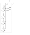
- FIG. 2 shows an example of a readout circuit for a unit pixel of the image pickup device shown in FIG.
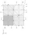
- FIG. 3 is a plan view illustrating an example of the configuration of the imaging device according to the first embodiment of the present disclosure.
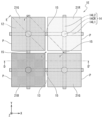
- FIG. 4 is a simplified view of the plan view shown in FIG. 3, and is a plan view showing the positional relationship between the inter-pixel isolation portions, the intra-pixel isolation portions, the connecting portions, and the color filters.
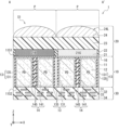
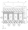
- FIG. 5 is a cross-sectional view taken along line AA' of the plan view shown in FIG.
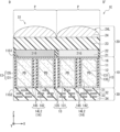
- FIG. 6 is a cross-sectional view taken along line BB' of the plan view shown in FIG. FIG.
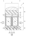
- FIG. 7 is a cross-sectional view taken along line CC' of the plan view shown in FIG.
- FIG. 8 is a plan view illustrating an imaging device according to a first modification of the first embodiment of the present disclosure.
- FIG. 9 is a plan view illustrating an imaging device according to a second modification of the first embodiment of the present disclosure.
- FIG. 10 is a plan view illustrating an imaging device according to a third modification of the first embodiment of the present disclosure.
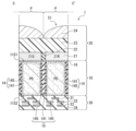
- FIG. 11 is a cross-sectional view illustrating a configuration example of an imaging device according to a second embodiment of the present disclosure.
- FIG. 12 is a plan view illustrating a configuration example of an imaging device according to a third embodiment of the present disclosure.
- FIG. 13 is a cross-sectional view illustrating a configuration example of an imaging device according to a third embodiment of the present disclosure.
- FIG. 14 is a cross-sectional view illustrating a configuration example of an imaging device according to a third embodiment of the present disclosure.
- FIG. 15 is a cross-sectional view illustrating a configuration example of an imaging device according to a third embodiment of the present disclosure.
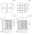
- FIG. 16A is a diagram showing a process sequence of a manufacturing method for an imaging device according to the fourth embodiment of the present disclosure.
- FIG. 16B is a diagram showing a manufacturing method of an imaging device according to the fourth embodiment of the present disclosure in the order of steps.
- FIG. 16C is a diagram showing a process sequence of a manufacturing method for an imaging device according to the fourth embodiment of the present disclosure.
- FIG. 16A is a diagram showing a process sequence of a manufacturing method for an imaging device according to the fourth embodiment of the present disclosure.
- FIG. 16B is a diagram showing a manufacturing method of an imaging
- FIG. 16D is a diagram showing a process sequence of a manufacturing method for an imaging device according to the fourth embodiment of the present disclosure.
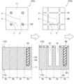
- FIG. 17 is a diagram showing a manufacturing method of an imaging device according to Modification 1 of the fourth embodiment of the present disclosure in the order of steps.
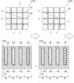
- FIG. 18A is a diagram showing a process sequence of a manufacturing method for an imaging device according to Modification 2 of Embodiment 4 of the present disclosure.
- FIG. 18B is a diagram showing a manufacturing method of an imaging device according to Modification 2 of Embodiment 4 of the present disclosure in the order of steps.
- FIG. 18C is a diagram showing a process sequence of a manufacturing method for an imaging device according to Modification 2 of Embodiment 4 of the present disclosure.
- FIG. 18A is a diagram showing a process sequence of a manufacturing method for an imaging device according to Modification 2 of Embodiment 4 of the present disclosure.
- FIG. 18B is a diagram showing a manufacturing method of an imaging device according to Modification 2 of
- FIG. 19A is a diagram showing a manufacturing method of an imaging device according to a fifth embodiment of the present disclosure in the order of steps.
- FIG. 19B is a diagram showing a manufacturing method of an imaging device according to the fifth embodiment of the present disclosure in the order of steps.
- FIG. 20A is a diagram showing a manufacturing method of an imaging device according to the sixth embodiment of the present disclosure in the order of steps.
- FIG. 20B is a diagram showing a manufacturing method of an imaging device according to the sixth embodiment of the present disclosure in the order of steps.
- FIG. 20C is a diagram showing a process sequence of a manufacturing method for an imaging device according to the sixth embodiment of the present disclosure.
- FIG. 20D is a diagram showing the process steps of a manufacturing method for an imaging device according to the sixth embodiment of the present disclosure.
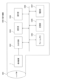
- FIG. 21 is a diagram showing a schematic configuration of an electronic device.
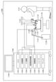
- FIG. 22 is a block diagram showing a schematic configuration example of a vehicle control system, which is an example of a mobile object control system to which the technology according to the present disclosure can be applied.
- FIG. 23 is a diagram showing an example of the installation position of the imaging unit.
- FIG. 24 is a diagram showing an example of a schematic configuration of an endoscopic surgery system to which the technology according to the present disclosure (the present technology) can be applied.
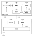
- FIG. 25 is a block diagram showing an example of the functional configuration of the camera head and the CCU shown in FIG. 24. As shown in FIG.
- directions may be described using the terms X-axis, Y-axis, and Z-axis.
- the Z-axis is the thickness direction of the semiconductor substrate 11, which will be described later.
- the X-axis and Y-axis are directions that are perpendicular to the Z-axis.
- the X-axis, Y-axis, and Z-axis are perpendicular to each other.
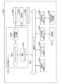
- FIG. 1 is a diagram showing an example of the overall configuration of an imaging device 1 according to an embodiment of the present disclosure.
- the imaging device 1 is an example of the "photodetection device" of the present disclosure, and is, for example, a CMOS (Complementary Metal Oxide Semiconductor) image sensor used in electronic devices such as digital still cameras and video cameras.
- the imaging device 1 has a pixel section (pixel section 100A) in which a plurality of pixels are two-dimensionally arranged in a matrix as an imaging area.
- the imaging device 1 is, for example, a back-illuminated imaging device in this CMOS image sensor or the like.
- the imaging device 1 takes in incident light (image light) from a subject via an optical lens system (not shown), converts the amount of incident light imaged on the imaging surface into an electrical signal on a pixel-by-pixel basis, and outputs it as a pixel signal.
- the imaging device 1 has a pixel section 100A as an imaging area on a semiconductor substrate 11, and also has, for example, a vertical drive circuit 111, a column signal processing circuit 112, a horizontal drive circuit 113, an output circuit 114, a control circuit 115, and an input/output terminal 116 in the peripheral area of this pixel section 100A.
- a plurality of unit pixels P are arranged two-dimensionally in a matrix.
- Each of the plurality of unit pixels P serves as both an imaging pixel and an image plane phase difference pixel.
- the imaging pixel photoelectrically converts the subject image formed by the imaging lens in a photodiode (PD) to generate a signal for generating an image.
- the image plane phase difference pixel divides the pupil region of the imaging lens, and photoelectrically converts the subject image from the divided pupil region to generate a signal for phase difference detection.
- a pixel drive line Lread (specifically, a row selection line and a reset control line) is wired for each pixel row, and a vertical signal line Lsig is wired for each pixel column.
- the pixel drive line Lread transmits a drive signal for reading out signals from the pixels.
- One end of the pixel drive line Lread is connected to an output terminal of the vertical drive circuit 111 corresponding to each row.
- the vertical drive circuit 111 is a pixel drive section that is composed of a shift register, an address decoder, etc., and drives each unit pixel P of the pixel section 100A, for example, row by row.
- the signals output from each unit pixel P of the pixel row selected and scanned by the vertical drive circuit 111 are supplied to the column signal processing circuit 112 through each vertical signal line Lsig.
- the column signal processing circuit 112 is composed of an amplifier, a horizontal selection switch, etc., provided for each vertical signal line Lsig.
- the horizontal drive circuit 113 is composed of a shift register, an address decoder, etc., and drives each horizontal selection switch of the column signal processing circuit 112 in sequence while scanning them. Through selective scanning by this horizontal drive circuit 113, the signals of each pixel transmitted through each of the vertical signal lines Lsig are output in sequence to the horizontal signal line 121, and transmitted to the outside of the semiconductor substrate 11 through the horizontal signal line 121.
- the output circuit 114 processes and outputs signals sequentially supplied from each of the column signal processing circuits 112 via the horizontal signal line 121.
- the output circuit 114 may perform only buffering, or may perform black level adjustment, column variation correction, various digital signal processing, etc., for example.
- the circuit portion consisting of the vertical drive circuit 111, column signal processing circuit 112, horizontal drive circuit 113, horizontal signal line 121, and output circuit 114 may be formed directly on the semiconductor substrate 11, or may be disposed on an external control IC. In addition, these circuit portions may be formed on other substrates connected by cables or the like.
- the control circuit 115 receives a clock and data instructing the operation mode provided from outside the semiconductor substrate 11, and also outputs data such as internal information of the imaging device 1.
- the control circuit 115 further has a timing generator that generates various timing signals, and controls the driving of peripheral circuits such as the vertical drive circuit 111, column signal processing circuit 112, and horizontal drive circuit 113 based on the various timing signals generated by the timing generator.
- the input/output terminal 116 is used to exchange signals with the outside world.
- Fig. 2 illustrates an example of a readout circuit for a unit pixel P of the imaging device 1 illustrated in Fig. 1.
- the unit pixel P includes, for example, four photoelectric conversion units 12A, 12B, 12C, and 12D, transfer transistors TR1, TR2, TR3, and TR4, a floating diffusion FD, a reset transistor RST, an amplification transistor AMP, and a selection transistor SEL.
- the photoelectric conversion units 12A, 12B, 12C, and 12D are each a photodiode (PD).
- the photoelectric conversion unit 12A has an anode connected to a ground voltage line and a cathode connected to the source of the transfer transistor TR1. Similar to the photoelectric conversion unit 12A, the photoelectric conversion units 12B, 12C, and 12D have an anode connected to a ground voltage line and a cathode connected to the sources of the transfer transistors TR2, TR3, and TR4.
- the transfer transistor TR1 is connected between the photoelectric conversion unit 12A and the floating diffusion FD.
- the transfer transistor TR2 is connected between the photoelectric conversion unit 12B and the floating diffusion FD.
- the transfer transistor TR3 is connected between the photoelectric conversion unit 12C and the floating diffusion FD.
- the transfer transistor TR4 is connected between the photoelectric conversion unit 12D and the floating diffusion FD.
- a drive signal TRsig is applied to each gate electrode of the transfer transistors TR1, TR2, TR3, and TR4.
- this drive signal TRsig becomes active, the transfer gates of the transfer transistors TR1, TR2, TR3, and TR4 become conductive, and the signal charges stored in the photoelectric conversion units 12A, 12B, 12C, and 12D are transferred to the floating diffusion FD via the transfer transistors TR1, TR2, TR3, and TR4.
- the floating diffusion FD is connected between the transfer transistors TR1, TR2, TR3, and TR4 and the amplification transistor AMP.
- the floating diffusion FD converts the signal charges transferred by the transfer transistors TR1, TR2, TR3, and TR4 into a voltage signal and outputs it to the amplification transistor AMP.
- the reset transistor RST is connected between the floating diffusion FD and the power supply unit.
- a drive signal RSTsig is applied to the gate electrode of the reset transistor RST.
- this drive signal RSTsig becomes active, the reset gate of the reset transistor RST becomes conductive, and the potential of the floating diffusion FD is reset to the level of the power supply unit.
- the amplifier transistor AMP has its gate electrode connected to the floating diffusion FD and its drain electrode connected to the power supply, and serves as the input of a readout circuit for the voltage signal held by the floating diffusion FD, a so-called source follower circuit.
- the amplifier transistor AMP has its source electrode connected to the vertical signal line Lsig via the selection transistor SEL, and thus constitutes a constant current source connected to one end of the vertical signal line Lsig and a source follower circuit.
- the selection transistor SEL is connected between the source electrode of the amplification transistor AMP and the vertical signal line Lsig.
- a drive signal SELsig is applied to the gate electrode of the selection transistor SEL.
- the selection transistor SEL becomes conductive and the unit pixel P becomes selected.
- the read signal (pixel signal) output from the amplification transistor AMP is output to the vertical signal line Lsig via the selection transistor SEL.
- the signal charges generated in the photoelectric conversion unit 12A, the signal charges generated in the photoelectric conversion unit 12B, the signal charges generated in the photoelectric conversion unit 12C, and the signal charges generated in the photoelectric conversion unit 12D are read out.
- the signal charges read out from each of these photoelectric conversion units 12A, 12B, 12C, and 12D to, for example, a phase difference calculation block of an external signal processing unit, a signal for phase difference autofocus can be obtained.
- FIG. 3 is a plan view showing a configuration example of the imaging device 1 according to the first embodiment of the present disclosure.
- Fig. 4 is a simplified view of the plan view shown in Fig. 3, and is a plan view showing the positional relationship between the inter-pixel isolation portion 13, the intra-pixel isolation portion 14, the connecting portion 15, and the color filter 21.
- the on-chip lens 24 shown in Fig. 3 is omitted.
- Fig. 5 is a cross-sectional view taken along line A-A' in the plan view shown in Fig. 4.
- Fig. 6 is a cross-sectional view taken along line B-B' in the plan view shown in Fig. 4.
- Fig. 7 is a cross-sectional view taken along line C-C' in the plan view shown in Fig. 4.
- the imaging device 1 shown in Figures 3 to 7 is, for example, a back-illuminated imaging device, as described above.
- the multiple unit pixels P arranged two-dimensionally in a matrix in the pixel section 100A each have, for example, a light receiving section 10, a light collecting section 20 provided on the first surface 11S1 side, which is the light incident surface of the light receiving section 10, and a multilayer wiring layer 30 provided on the second surface 11S2 side, which is the opposite side to the first surface 11S1 of the light receiving section 10.
- the imaging device 1 is a back-illuminated type
- the first surface 11S1 corresponds to the back surface
- the second surface 11S2 corresponds to the front surface.
- the light receiving unit 10 has a semiconductor substrate 11 having a first surface 11S1 and a second surface 11S2 facing each other, and a plurality of photoelectric conversion units 12 embedded in the semiconductor substrate 11.
- the semiconductor substrate 11 is, for example, made of a silicon substrate.
- the photoelectric conversion units 12 are, for example, PIN (Positive Intrinsic Negative) type photodiodes (PD) and have a pn junction in a predetermined region of the semiconductor substrate 11.
- a plurality of photoelectric conversion units 12 are embedded in the unit pixel P.
- four photoelectric conversion units 12A, 12B, 12C, and 12D are embedded in the unit pixel P.
- the light receiving section 10 further has an inter-pixel isolation section 13, an intra-pixel isolation section 14, and a connection section 15.
- the inter-pixel isolation section 13 is provided between adjacent unit pixels P. In other words, the inter-pixel isolation section 13 is provided around the unit pixels P.
- the inter-pixel isolation section 13 is provided in a lattice shape in a plan view, as shown in, for example, Figures 3 and 4.
- the inter-pixel isolation section 13 is for electrically and optically isolating adjacent unit pixels P.
- the inter-pixel isolation section 13 penetrates between the first surface 11S1 and the second surface 11S2 of the semiconductor substrate 11, for example, along the thickness direction of the semiconductor substrate 11 (for example, the Z-axis direction).
- the pixel separation portion 13 has a gap 131 and an insulating film 135 (an example of a "first insulating film” in this disclosure) provided between the gap 131 and the semiconductor substrate 11.
- the gap 131 is a slit that penetrates between the first surface 11S1 and the second surface 11S2 of the semiconductor substrate 11.
- the insulating film 135 is provided around this slit (i.e., the gap 131). As shown in FIG. 4, this slit (i.e., the gap 131) is provided in a lattice shape in a plan view.
- the gap 131 may also be referred to as an air layer.
- the insulating film 135 is, for example, a silicon oxide (SiOx), aluminum oxide (AlOx), or hafnium oxide (HfOx) film.
- SiOx silicon oxide
- AlOx aluminum oxide
- HfOx hafnium oxide
- the insulating film 135 can be made into a pinning film having a negative fixed charge.
- the electric field induced by this pinning film can form a hole accumulation layer in the semiconductor substrate 11 that contacts the pinning film, and the generation of dark current due to the interface state of the semiconductor substrate 11 that contacts the pinning film can be suppressed.
- the inter-pixel separation section 13 is located in a planar view between a unit pixel P that overlaps with the red color filter 21R and a unit pixel P that overlaps with the green color filter 21G, and between a unit pixel P that overlaps with the blue color filter 21B and a unit pixel P that overlaps with the green color filter 21G.
- the inter-pixel separation section 13 separates different colors in a planar view. For this reason, the inter-pixel separation section 13 may be referred to as a "different color separation section.”
- the intra-pixel isolation portion 14 is provided between adjacent photoelectric conversion portions 12A, 12B, 12C, and 12D within a unit pixel P.
- the intra-pixel isolation portion 14 serves to electrically isolate adjacent photoelectric conversion portions 12A, 12B, 12C, and 12D.
- the intra-pixel isolation portion 14 is provided in a lattice pattern in a plan view.
- the intra-pixel isolation portion 14 like the inter-pixel isolation portion 13, penetrates between the first surface 11S1 and the second surface 11S2 of the semiconductor substrate 11 along the thickness direction of the semiconductor substrate 11 (e.g., the Z-axis direction).
- the pixel isolation portion 14 has a first material layer 141 and an insulating film 145 (an example of a "second insulating film” in this disclosure) provided between the first material layer 141 and the semiconductor substrate 11.
- the first material layer 141 penetrates between the first surface 11S1 and the second surface 11S2 of the semiconductor substrate 11.
- the insulating film 145 is provided around the first material layer 141.
- the first material layer 141 is preferably made of a material having a refractive index close to that of the semiconductor substrate 11, for example, a material having a refractive index that is 0.6 to 1.4 times that of the semiconductor substrate 11. Since the semiconductor substrate 11 is silicon (Si), the first material layer 141 is preferably made of a material having a refractive index close to that of silicon, for example, a material having a refractive index that is 0.6 to 1.4 times that of the refractive index of silicon. Examples of the first material layer 141 that satisfies such conditions include titanium oxide (TiOx; for example, TiO 2 ), iron oxide (FexOy; for example, Fe 2 O 3 ), or a laminated film of titanium oxide and iron oxide.
- TiOx titanium oxide
- FeOy iron oxide
- Fe 2 O 3 iron oxide
- the first material layer 141 is made of a material (e.g., TiO2 , Fe2O3 ) having a refractive index close to that of the semiconductor substrate 11, reflection of light between the first material layer 141 and the semiconductor substrate 11 can be suppressed, thereby improving the optical characteristics of the unit pixel P.
- a material e.g., TiO2 , Fe2O3
- the first material layer 141 is not limited to TiOx or FexOy, and may be, for example, SiOx (e.g., SiO 2 ) or SiNx (e.g., Si 3 N 4 ), or a laminated film of SiOx and SiNx.
- the first material layer 141 may be one or more of tantalum oxide (TaOx), diamond, zirconium oxide (ZrOx), hafnium oxide (HfOx), cerium oxide (CeOx), aluminum oxide (AlOx), and niobium oxide (NbOx).
- the first material layer 141 may be non-doped polysilicon (Poly-Si) or amorphous silicon (a-Si).
- the insulating film 145 is, for example, a silicon oxide (SiOx), aluminum oxide (AlOx), or hafnium oxide (HfOx) film.
- SiOx silicon oxide
- AlOx aluminum oxide
- HfOx hafnium oxide
- the insulating film 145 can be made into a pinning film having a negative fixed charge.
- the electric field induced by this pinning film can form a hole accumulation layer in the semiconductor substrate 11 that contacts the pinning film, and the generation of dark current due to the interface state of the semiconductor substrate 11 that contacts the pinning film can be suppressed.
- the intra-pixel separation section 14 is located between the photoelectric conversion sections 12A, 12B, 12C, and 12D that overlap with the color filters 21 of the same color in a planar view.
- the intra-pixel separation section 14 separates the same colors in a planar view. For this reason, the intra-pixel separation section 14 may be referred to as a "same-color separation section.”
- the connecting portion 15 is provided between adjacent unit pixels P and connects the intra-pixel isolation portion 14 of one adjacent unit pixel P to the intra-pixel isolation portion 14 of the other adjacent unit pixel P.
- the connecting portion 15 is formed integrally with the intra-pixel isolation portion 14.
- the connecting portion 15 has, for example, a first material layer 141 and an insulating film 145.
- the first material layer 141 of the connecting portion 15 has the same composition as the first material layer 141 of the intra-pixel isolation portion 14.
- the first material layer 141 of the connecting portion 15 is formed integrally with the first material layer 141 of the intra-pixel isolation portion 14.
- the insulating film 145 of the connecting portion 15 has the same composition as the insulating film 145 of the intra-pixel isolation portion 14.
- the insulating film 145 of the connecting portion 15 is formed integrally with the insulating film 145 of the intra-pixel isolation portion 14.
- the first surface 11S1 of the semiconductor substrate 11 is provided with a fixed charge layer 16 that also serves to prevent reflection on the first surface 11S1 of the semiconductor substrate 11.
- the fixed charge layer 16 may be a film having a positive fixed charge, or a film having a negative fixed charge.
- Examples of the material constituting the fixed charge layer 16 include semiconductor materials or conductive materials having a band gap wider than the band gap of the semiconductor substrate 11.
- examples of the material include hafnium oxide (HfOx), aluminum oxide (AlOx), zirconium oxide (ZrOx), tantalum oxide (TaOx), titanium oxide (TiOx), lanthanum oxide (LaOx), praseodymium oxide (PrOx), cerium oxide (CeOx), neodymium oxide (NdOx), promethium oxide (PmOx), samarium oxide (SmOx), europium oxide (EuOx), gallium oxide (GaOx), and the like.
- the fixed charge layer 16 may be a single layer film or a laminated film made of different materials.
- the light-collecting section 20 is provided on the first surface 11S1 of the light-receiving section 10, and includes a color filter 21 that selectively transmits a color preset for each unit pixel P, such as red light (R), green light (G), or blue light (B), a light-shielding section 22 provided between the unit pixels P of the color filter 21, a planarization layer 23, and a lens layer 24L, which are stacked in this order from the light-receiving section 10 side.
- a color filter 21 that selectively transmits a color preset for each unit pixel P, such as red light (R), green light (G), or blue light (B)
- a light-shielding section 22 provided between the unit pixels P of the color filter 21, a planarization layer 23, and a lens layer 24L, which are stacked in this order from the light-receiving section 10 side.
- the color filters 21 are arranged diagonally with two color filters 21G that selectively transmit green light (G), and one color filter 21R, 21B that selectively transmit red light (R) and blue light (B) arranged on each of the orthogonal diagonals.
- the unit pixels P provided with the color filters 21R, 21G, 21B for example, the corresponding color light is detected in each photoelectric conversion section 12. That is, in the pixel section 100A, the unit pixels P that detect red light (R), green light (G), and blue light (B), respectively, are arranged in a Bayer pattern.
- the light shielding portions 22 are intended to prevent light incident obliquely on the color filter 21 from leaking into adjacent unit pixels P, and are provided between the unit pixels P of the color filter 21 as described above. In other words, the light shielding portions 22 are provided in a lattice pattern in the pixel section 100A.
- Examples of materials that constitute the light shielding portions 22 include conductive materials that have light shielding properties. Specific examples include tungsten (W), silver (Ag), copper (Cu), aluminum (Al), and alloys of Al and copper (Cu).
- the planarization layer 23 is intended to planarize the surface of the light incident side S1, which is formed by the color filter 21 and the light shielding portion 22.
- the planarization layer 23 is formed using, for example, silicon oxide (SiOx), silicon nitride (SiNx), silicon oxynitride (SiOxNy), etc.
- the lens layer 24L is provided so as to cover the entire surface of the pixel section 100A, and has, for example, a plurality of on-chip lenses 24 arranged in a gapless manner on its surface.
- the on-chip lenses 24 are for focusing light incident from above onto the photoelectric conversion section 12, and are provided, for example, for each unit pixel P. That is, the on-chip lenses 24 are provided across the multiple photoelectric conversion sections 12 in the unit pixel P.
- the inter-pixel separation section 13 and the boundaries of the multiple on-chip lenses 24 approximately coincide with each other.
- the lens layer 24L is formed of an inorganic material such as silicon oxide (SiOx) or silicon nitride (SiNx). Alternatively, the lens layer 24L may be formed using an organic material with a high refractive index such as an episulfide resin, a thietane compound or a resin thereof.
- the shape of the on-chip lens 24 is not particularly limited, and various lens shapes such as a hemispherical shape or a semicylindrical shape can be used.
- the multi-layer wiring layer 30 is provided on the side opposite to the first surface 11S1 of the light receiving section 10, specifically, on the second surface 11S2 side of the semiconductor substrate 11.
- the multi-layer wiring layer 30 has a configuration in which, for example, a plurality of wiring layers 31, 32, and 33 are stacked with an interlayer insulating layer 34 between them.
- the multi-layer wiring layer 30 also has, for example, a vertical drive circuit 111, a column signal processing circuit 112, a horizontal drive circuit 113, an output circuit 114, a control circuit 115, and input/output terminals 116 formed therein.
- the wiring layers 31, 32, and 33 are formed using, for example, aluminum (Al), copper (Cu), or tungsten (W). Alternatively, the wiring layers 31, 32, and 33 may be formed using polysilicon (Poly-Si).
- the interlayer insulating layer 34 is formed, for example, of a single layer film made of one of silicon oxide (SiOx), TEOS, silicon nitride (SiNx), silicon oxynitride (SiOxNy), etc., or a laminate film made of two or more of these.
- the imaging device 1 has a first surface 11S1 and a second surface 11S2 located on the opposite side of the first surface 11S1, and is equipped with a semiconductor substrate 11 on which a plurality of unit pixels P are arranged in a matrix and on which a plurality of photoelectric conversion units 12 are provided for each unit pixel P, the photoelectric conversion units 12 generating an electric charge corresponding to the amount of received light through photoelectric conversion, an inter-pixel separation unit 13 provided between adjacent unit pixels P and having a gap portion 131 that electrically and optically separates the adjacent unit pixels P, an intra-pixel separation unit 14 provided between adjacent photoelectric conversion units 12A, 12B, 12C, and 12D within the unit pixel P and having a first material layer 141 that electrically separates the adjacent photoelectric conversion units 12, and a connecting unit 15 provided between adjacent unit pixels P and connecting the intra-pixel separation unit 14 of one adjacent unit pixel P to the intra-pixel separation unit 14 of
- the gap 131 of the inter-pixel separation section 13 can totally reflect the light that enters the unit pixel P, confining it within the unit pixel P. This can suppress color mixing between adjacent unit pixels P.
- a material with a refractive index close to that of the material (e.g., silicon) that constitutes the semiconductor substrate 11 can be used as the first material layer 141 of the intra-pixel separation section 14. This can suppress reflection and scattering of light between adjacent photoelectric conversion sections 12A, 12B, 12C, and 12D within the unit pixel P. From the above, the imaging device 1 can improve its optical characteristics.
- the aspect ratio of the void 131 in the inter-pixel isolation 13 will increase. If the aspect ratio of the void 131 increases, the pattern including the intra-pixel isolation 14 will be more likely to collapse, for example, during a cleaning or etching process using a liquid or during a drying process after cleaning or etching.
- the intra-pixel isolation 14 of one adjacent unit pixel P is connected to the intra-pixel isolation 14 of the other unit pixel P by a connecting portion 15 disposed between the unit pixels P. This makes it possible to suppress pattern collapse.
- one unit pixel P has four photoelectric conversion units 12A, 12B, 12C, and 12D.
- the unit pixel P shown in Fig. 4 is also referred to as a 2 x 2 type in this specification because the four photoelectric conversion units 12A, 12B, 12C, and 12D are arranged in pairs in the X-axis direction and in the Y-axis direction.
- the configuration of the unit pixel P is not limited to the 2 x 2 type.
- Modification 1 Fig. 8 is a plan view showing an imaging device 1A according to Modification 1 of the embodiment 1 of the present disclosure.
- the imaging device 1A shown in Fig. 8 is an example of the "photodetection device" of the present disclosure.
- each of the multiple unit pixels P has two photoelectric conversion units 12A, 12B.
- the unit pixel P shown in Fig. 8 is also referred to as a 2x1 type in this specification because the two photoelectric conversion units 12A, 12B are aligned in the X-axis direction but not aligned in the Y-axis direction.
- the imaging device 1A having a 2 ⁇ 1 type unit pixel P shown in FIG. 8 includes an inter-pixel separation section 13 provided between adjacent unit pixels P and having a gap section 131 that electrically and optically separates the adjacent unit pixels P, an intra-pixel separation section 14 provided between adjacent photoelectric conversion sections 12A, 12B within the unit pixel P and having a first material layer 141 that electrically separates the adjacent photoelectric conversion sections 12, and a connecting section 15 provided between adjacent unit pixels P and connecting the intra-pixel separation section 14 of one adjacent unit pixel P to the intra-pixel separation section 14 of the other adjacent unit pixel P.
- the imaging device 1A can prevent color mixing between adjacent unit pixels P and suppress light reflection and scattering between adjacent photoelectric conversion sections 12A, 12B within the unit pixel P. Furthermore, because the connecting section 15 connects the intra-pixel separation section 14 of one adjacent unit pixel P to the intra-pixel separation section 14 of the other unit pixel P, the imaging device can suppress pattern collapse even when the aspect ratio of the gap section 131 becomes high.
- FIG. 9 is a plan view showing an imaging device 1B according to Modification 2 of the first embodiment of the present disclosure.
- the imaging device 1B shown in Fig. 9 is an example of the "photodetection device" of the present disclosure.
- each of the multiple unit pixels P has nine photoelectric conversion units 12.
- the unit pixel P shown in Fig. 9 is also referred to as a 3x3 type in this specification because the nine photoelectric conversion units 12 are arranged in threes in the X-axis direction and threes in the Y-axis direction.
- the imaging device 1B having a 3x3 type unit pixel P shown in FIG. 9 has an inter-pixel separation section 13 having a void section 131, an intra-pixel separation section 14 having a first material layer 141, and a connecting section 15.
- the imaging device 1B can prevent color mixing between adjacent unit pixels P and suppress light reflection and scattering between multiple (e.g., nine) adjacent photoelectric conversion sections 12 within the unit pixel P.
- the connecting section 15 connects the intra-pixel separation section 14 of one adjacent unit pixel P to the intra-pixel separation section 14 of the other unit pixel P, the imaging device 1B can suppress pattern collapse even when the aspect ratio of the void section 131 becomes high.
- FIG. 10 is a plan view illustrating an imaging device 1C according to Modification 3 of the first embodiment of the present disclosure.
- the imaging device 1C illustrated in Fig. 10 is an example of the "photodetection device" of the present disclosure.
- each of the multiple unit pixels P has 16 photoelectric conversion units 12.
- the unit pixel P illustrated in Fig. 10 is also referred to as a 4x4 type in this specification because the 16 photoelectric conversion units 12 are arranged in four each in the X-axis direction and the Y-axis direction.
- the imaging device 1C having a 4x4 type unit pixel P shown in FIG. 10 has an inter-pixel separation section 13 having a gap 131, an intra-pixel separation section 14 having a first material layer 141, and a connecting section 15.
- the imaging device 1C can prevent color mixing between adjacent unit pixels P and suppress light reflection and scattering between multiple (e.g., 16) adjacent photoelectric conversion sections 12 within the unit pixel P.
- the connecting section 15 connects the intra-pixel separation section 14 of one adjacent unit pixel P to the intra-pixel separation section 14 of the other unit pixel P, the imaging device 1C can suppress pattern collapse even when the aspect ratio of the gap 131 becomes high.
- the inter-pixel isolation portion 13 and the intra-pixel isolation portion 14 each penetrate between the first surface 11S1 and the second surface 11S2 of the semiconductor substrate 11 along the thickness direction (e.g., the Z-axis direction) of the semiconductor substrate 11.
- the embodiments of the present disclosure are not limited to this. At least one of the inter-pixel isolation portion 13 and the intra-pixel isolation portion 14 does not have to penetrate the semiconductor substrate 11.
- FIG. 11 is a cross-sectional view showing an example of the configuration of an imaging device 1D according to embodiment 2 of the present disclosure.
- the imaging device 1D shown in FIG. 11 differs from the imaging device 1 shown in FIG. 5 etc. in that the inter-pixel isolation portion 13 and the intra-pixel isolation portion 14 do not penetrate the semiconductor substrate 11.
- the inter-pixel isolation portion 13 and the intra-pixel isolation portion 14 are provided from the first surface 11S1 side of the semiconductor substrate 11 to a midway position in the thickness direction (e.g., the Z-axis direction) of the semiconductor substrate 11.
- the imaging device 1D is, for example, a back-illuminated type
- the first surface 11S1 corresponds to the back surface.
- the pixel separation portion 13 has a gap 131 and an insulating film 135 provided between the gap 131 and the semiconductor substrate 11.
- the gap 131 and the insulating film 135 are provided from the first surface 11S1 side, which corresponds to the back surface of the semiconductor substrate 11, to a midway position in the thickness direction (e.g., the Z-axis direction) of the semiconductor substrate 11.
- the gap 131 and the insulating film 135 do not reach the second surface 11S2 side, which corresponds to the front surface of the semiconductor substrate 11.
- the intra-pixel isolation portion 14 has a first material layer 141 and an insulating film 145 provided between the first material layer 141 and the semiconductor substrate 11.
- the first material layer 141 and the insulating film 145 are provided from the first surface 11S1 side, which corresponds to the back surface of the semiconductor substrate 11, to a position midway in the thickness direction (e.g., the Z-axis direction) of the semiconductor substrate 11.
- the first material layer 141 and the insulating film 145 do not reach the second surface 11S2 side, which corresponds to the front surface of the semiconductor substrate 11.
- the structure of the unit pixel P of the imaging device 1D in a plan view is the same as the structure of the unit pixel P of the imaging device 1 shown in, for example, Figures 3 and 4 in a plan view. Also, in embodiment 2, the configurations of variants 1 to 3 of embodiment 1 can be applied.
- the unit pixel P of the imaging device 1D is not limited to the 2x2 type shown in Figures 3 and 4, but may be, for example, the 2x1 type shown in Figure 8, the 3x3 type shown in Figure 9, or the 4x4 type shown in Figure 10.
- the imaging device 1D includes an inter-pixel separation section 13 having a void section 131, an intra-pixel separation section 14 having a first material layer 141, and a connecting section 15. As a result, like the imaging device 1, the imaging device 1D can prevent color mixing between adjacent unit pixels P and suppress light reflection and scattering between adjacent photoelectric conversion sections 12 within the unit pixel P. Furthermore, since the connecting section 15 connects the intra-pixel separation section 14 of one adjacent unit pixel P to the intra-pixel separation section 14 of the other unit pixel P, the imaging device 1D can suppress pattern collapse even when the aspect ratio of the void section 131 becomes high.
- the intra-pixel separation portion 14 (i.e., the same-color separation portion) has a lattice-like shape in plan view.
- the lattice-like intra-pixel separation portion 14 may have intersections and straight portions made of different materials.
- FIG. 12 is a plan view showing an example of the configuration of an imaging device 1E according to embodiment 3 of the present disclosure.
- FIGS. 13 to 15 are cross-sectional views showing an example of the configuration of an imaging device 1E according to embodiment 3 of the present disclosure.
- FIG. 13 is a cross-sectional view taken along line D-D' in the plan view shown in FIG. 12.
- FIG. 14 is a cross-sectional view taken along line E-E' in the plan view shown in FIG. 12.
- FIG. 15 is a cross-sectional view taken along line F-F' in the plan view shown in FIG. 12. Note that the on-chip lens 24 shown in FIGS. 13 to 15 is omitted in FIG. 12.
- the intra-pixel separation portion 14 in a plan view from the thickness direction (e.g., the Z-axis direction) of the semiconductor substrate 11, has a first straight portion 14L1 extending in the X-axis direction (an example of the "first direction” in this disclosure), a second straight portion 14L2 extending in the Y-axis direction (an example of the "second direction” in this disclosure) perpendicular to the X-axis direction, and an intersection portion 14CR located in the region where the first straight portion 14L1 and the second straight portion 14L2 intersect.
- the first straight portion 14L1, the second straight portion 14L2, and the connecting portion 15 are made of the same material.
- the intersection portion 14CR is made of a different material from the first straight portion 14L1, the second straight portion 14L2, and the connecting portion 15.
- the intra-pixel isolation portion 14 has, as a first material layer, a second material layer 142 used for the first straight portion 14L1, the second straight portion 14L2, and the coupling portion 15, and a third material layer 143 used for the intersection portion 14CR.
- the second material layer 142 has a boron-doped amorphous silicon (BDAS) layer.
- the boron (B) concentration in the BDAS layer is, for example, 1 ⁇ 10 18 cm ⁇ 3 or more. This makes it possible to strengthen the pinning of the sidewalls of the trenches in which the first straight portion 14L1 and the second straight portion 14L2 are disposed.
- the third material layer 143 also has a material layer with a refractive index close to that of silicon (Si) constituting the semiconductor substrate 11, for example at least one of a titanium oxide layer and an iron oxide layer.
- the refractive index difference between the third material layer 143 and the semiconductor substrate 11 is greater than the refractive index difference between the second material layer and the semiconductor substrate. This makes it possible to suppress reflection and scattering of light even at the intersection 14CR, where light reflection and scattering are relatively likely to occur due to the structure.
- the imaging device 1E includes an inter-pixel separation section 13 having a gap section 131, an intra-pixel separation section 14 having a second material layer 142 and a third material layer 143 as a first material layer, and a connection section 15.
- This allows the imaging device 1E to prevent color mixing between adjacent unit pixels P, and to suppress light reflection and scattering between adjacent photoelectric conversion sections 12 within the unit pixel P.
- the pinning of the trench sidewalls is strengthened at the first straight section 14L1 and the second straight section 14L2 of the intra-pixel separation section 14, and light reflection and scattering can be suppressed at the intersection section 14CR.
- the connecting portion 15 connects the intra-pixel isolation portion 14 of one adjacent unit pixel P to the intra-pixel isolation portion 14 of the other adjacent unit pixel P, so that pattern collapse can be suppressed even when the aspect ratio of the void portion 131 becomes high.
- the unit pixels P of the imaging device 1E are not limited to the 2 ⁇ 2 type shown in FIGS. 3 and 4, but may be, for example, the 2 ⁇ 1 type shown in FIG. 8, the 3 ⁇ 3 type shown in FIG. 9, or the 4 ⁇ 4 type shown in FIG. 10.
- the imaging device is manufactured using various devices such as a resist coating device, an exposure device, an etching device, an ion implantation device, a film formation device, etc.
- these devices will be collectively referred to as manufacturing devices.
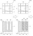
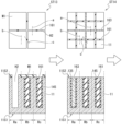
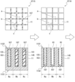
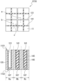
- 16A to 16D are diagrams showing the manufacturing method of an imaging device according to embodiment 4 of the present disclosure in the order of steps.
- the upper diagrams are plan views and the lower diagrams are cross-sectional views.
- line a is a line that intersects with the region where the lattice-shaped inter-pixel separation section 13 (different color separation section) is formed.
- Line b is a line that intersects with the region where the lattice-shaped intra-pixel separation section 14 (same color separation section) is formed.
- Line c is a line that intersects with the connecting direction of the region where the connecting section 15 that connects the intra-pixel separation section 14 (same color separation section) between adjacent unit pixels P is formed.
- region Ra in the cross-sectional view at the bottom indicates the region along line a
- region Rb indicates the region along line b
- region Rc indicates the region along line c. Note that in the cross-sectional view at the bottom, regions Ra, Rb, and Rc are shown lined up in one direction, but this is a schematic depiction due to space limitations. Regions Ra, Rb, and Rc are not actually lined up in one direction. The actual positions of regions Ra, Rb, and Rc overlap with lines a, b, and c shown in the plan view at the top.
- the manufacturing equipment partially etches the semiconductor substrate 11 from the second surface 11S2 side, which is the front surface of the semiconductor substrate 11, to form a slit H1.
- the slit H1 is formed in a region Rb where the intra-pixel isolation portion 14 is formed, and in a region Rc where the connection portion 15 is formed.
- the manufacturing equipment deposits an insulating film 145 and a material film 161 in this order on the second surface 11S2 side of the semiconductor substrate 11 to fill the slits H1 in the regions Rb and Rc.
- the insulating film 145 is a pinning film on the sidewalls of the slits.
- the material film 161 is preferably a material that has dry etching selectivity with respect to silicon (Si) constituting the semiconductor substrate 11, and is preferably, for example, Si3N4 or SiO2 .
- the manufacturing equipment then performs, for example, a CMP process on the second surface 11S2 side of the semiconductor substrate 11 to remove the material film 161 and the insulating film 145 from the second surface 11S2.
- a CMP process on the second surface 11S2 side of the semiconductor substrate 11 to remove the material film 161 and the insulating film 145 from the second surface 11S2.
- the manufacturing equipment forms a mask M1 on the second surface 11S2 of the semiconductor substrate 11.
- the mask M1 has a shape that covers the region Rb where the intra-pixel isolation portion 14 is formed, and exposes the region Rc where the connecting portion 15 is formed, and the region Ra where the inter-pixel isolation portion 13 is formed.
- the mask M1 has a shape that covers the unit pixels P and exposes the space between adjacent unit pixels P.
- the material that constitutes the mask M1 is, for example, SiOx, SiNx, or amorphous carbon (a-C).
- the manufacturing equipment then etches region Ra exposed from mask M1 to form slit H2 in region Ra.
- semiconductor substrate 11 is wet-etched or dry-etched under conditions in which the silicon that constitutes semiconductor substrate 11 is easily etched, and material film 161 and insulating film 145 that fill region Rc, and mask M1 are difficult to etch.
- Material film 161 and insulating film 145 in region Rc exposed from under mask M1 are barely etched, and are left in slit H1.
- the manufacturing equipment deposits the insulating film 135 and the material film 163 in this order on the second surface 11S2 side of the semiconductor substrate 11 to fill the slits H2 in the region Ra.
- the material film 163 is, for example, polysilicon (Poly-Si).
- the manufacturing equipment performs, for example, a CMP process on the second surface 11S2 side of the semiconductor substrate 11 to remove the material film 163, the insulating film 135, and the mask M1 from above the second surface 11S2.
- the region Ra where the inter-pixel isolation portion 13 is to be formed is filled with the material film 163 and the insulating film 135, and the material film 163 and the insulating film 135 are removed from above the second surface 11S2 in other regions.
- the manufacturing equipment simultaneously (or separately) recesses the material films 163, 165 from the second surface 11S2 side of the semiconductor substrate 11.
- the recesses may be etched back.
- the manufacturing equipment fills the recesses created by the recesses with an insulating film 167.
- the insulating film 167 is, for example, SiOx or SiNx.
- the FEOL (Front End of Line) process is completed for the process of forming the inter-pixel isolation portion 13, the intra-pixel isolation portion 14, and the connecting portion 15.
- step ST16 the manufacturing equipment performs a wet etching process using an alkaline solution on the first surface 11S1, which is the back surface of the semiconductor substrate 11, to expose the material films 161, 163 on the first surface 11S1 side.
- silicon (Si) that constitutes the semiconductor substrate 11 is etched, but the material film 163 (e.g., polysilicon) is difficult to etch.
- the manufacturing equipment etches the material film 161 under conditions in which the material film 161 is easily etched and the material film 164 and the semiconductor substrate 11 are difficult to etch. This removes the material film 161 from the slit H1 in the region Rb where the intra-pixel isolation portion 14 is formed, and from the slit H1 in the region Rc where the connection portion 15 is formed.
- the manufacturing equipment deposits a first material layer 141 on the first surface 11S1 side of the semiconductor substrate 11 to fill the slits H1 in the regions Rb and Rc .
- the first material layer 141 is, for example, TiO2 or Fe2O3 .
- the manufacturing equipment then performs, for example, a CMP process on the first surface 11S1 side of the semiconductor substrate 11 to remove the first material layer 141 from above the first surface 11S1.
- a CMP process on the first surface 11S1 side of the semiconductor substrate 11 to remove the first material layer 141 from above the first surface 11S1.
- the region Rb where the intra-pixel isolation portion 14 is to be formed and the region Rc where the connection portion 15 is to be formed are filled with the first material layer 141, and the first material layer 141 is removed from above the first surface 11S1 in other regions.
- the manufacturing equipment etches and removes the material film 163 embedded in the region Ra in which the inter-pixel isolation portion 13 is to be formed, to form the void portion 131.
- the material film 163 is, for example, polysilicon
- the first material layer 141 is, for example, TiO2 or Fe2O3 . For this reason, it is possible to remove the material film 163 by wet etching without etching the first material layer 141.
- a material film 161 is embedded in each slit H1 in the region Rb where the intra-pixel isolation portion 14 is formed and in the region Rc where the connecting portion is formed (step ST12). Then, in the back surface process, the material film 161 is removed from within the slit H1 (step ST16), and the first material layer 141 is embedded in the slit H1 from which the material film 161 has been removed. For example, compared to forming the first material layer 141 in the FEOL process rather than the back surface process, the possibility of contamination of the first material layer 141 can be reduced.
- the first material layer 141 When the first material layer 141 is formed in the FEOL process, it is necessary to select a material having high heat resistance for the first material layer 141 in consideration of the heat treatment temperature in the annealing process of the source/drain, etc. However, in the manufacturing method of the first embodiment, the first material layer 141 is formed in a back surface process after the high-temperature annealing process. Therefore, a material with a relatively low heat resistance can be used for the first material layer 141. This allows a wider range of material options for the first material layer 141.
- the material film 161 (e.g., SiN or SiO 2 ) filled in each slit H1 in the regions Rb and Rc in the FEOL process may be left as it is as a first material layer.
- the material film 161 is an example of the "first material layer" of the present disclosure.
- FIG. 17 is a diagram showing the process sequence of a manufacturing method for an imaging device according to Variation 1 of Embodiment 4 of the present disclosure.
- steps ST21 and ST22 shown in FIG. 17 the upper figures show plan views and the lower figures show cross-sectional views.
- Step ST21 in FIG. 17 is the same as step ST16 in embodiment 4 up to the process of subjecting the first surface 11S1, which is the back surface of the semiconductor substrate 11, to a wet etching process using an alkaline solution to expose material films 161 and 163 on the first surface 11S1 side.
- the manufacturing equipment After exposing the material films 161 and 163 on the first surface 11S1 side, as shown in step ST22 of Fig. 17, the manufacturing equipment etches and removes the material film 163 embedded in the region Ra to form the void portion 131.
- the material film 163 is, for example, polysilicon
- the first material layer 141 is, for example, TiO2 or Fe2O3 . Therefore, it is possible to remove the material film 163 by wet etching without etching the first material layer 141.
- the inter-pixel isolation portion 13, the intra-pixel isolation portion 14, and the connecting portion 15 are completed.
- the material film 161 remaining in the regions Rb and Rc is an example of the "first insulating film" of the present disclosure. According to this modification 1, it is possible to shorten and simplify the manufacturing process compared to the manufacturing method of the above-mentioned embodiment 4.
- the first material layer 141 such as TiO2 or Fe2O3 may be embedded in each slit H1 of the regions Rb and Rc, instead of the material film 161 such as SiN or SiO2 .
- This may narrow the range of material selection for the first material layer 141, or may require a lower temperature for the thermal history, but on the other hand, since the process of forming the material film 161 is unnecessary, the manufacturing process can be shortened and simplified.
- this modified example 2 will be described in the order of the processes using the drawings.
- FIGS. 18A to 18C are diagrams showing the process sequence of a manufacturing method for an imaging device according to Variation 2 of Embodiment 4 of the present disclosure.
- steps ST31 to ST35 shown in FIGS. 18A to 18C the upper figures show plan views and the lower figures show cross-sectional views.
- step ST31 of FIG. 18A the process up to the step of forming slits H1 in regions Rb and Rc of semiconductor substrate 11 is the same as step ST16 of embodiment 4.
- the manufacturing equipment deposits an insulating film 145 and a first material layer 141 in this order on the second surface 11S2 side of the semiconductor substrate 11 to fill the slits H1 in the regions Rb and Rc .
- the first material layer 141 is, for example, TiO2 or Fe2O3 .
- the manufacturing equipment then performs, for example, a CMP process on the second surface 11S2 side of the semiconductor substrate 11 to remove the first material layer 141 and the insulating film 145 from the second surface 11S2.
- a CMP process on the second surface 11S2 side of the semiconductor substrate 11 to remove the first material layer 141 and the insulating film 145 from the second surface 11S2.
- the manufacturing equipment forms a mask M1 on the second surface 11S2 of the semiconductor substrate 11.
- the mask M1 has a shape that covers the region Rb where the intra-pixel isolation portion 14 is formed, and exposes the region Rc where the connecting portion 15 is formed, and the region Ra where the inter-pixel isolation portion 13 is formed.
- the material that constitutes the mask M1 is, for example, SiOx, SiNx, or amorphous carbon (a-C).
- the manufacturing equipment then etches region Ra exposed from mask M1 to form slit H2 in region Ra.
- the semiconductor substrate 11 is wet-etched or dry-etched under conditions in which the silicon that constitutes the semiconductor substrate 11 is easily etched, and the first material layer 141 and insulating film 145 that fill region Rc, and mask M1 are difficult to etch.
- the first material layer 141 and insulating film 145 in region Rc that are exposed from under mask M1 are barely etched and are left in slit H1.
- the manufacturing equipment deposits the insulating film 135 and the material film 163 in this order on the second surface 11S2 side of the semiconductor substrate 11 to fill the slits H2 in the region Ra.
- the material film 163 is, for example, polysilicon (Poly-Si).
- the manufacturing equipment performs, for example, a CMP process on the second surface 11S2 side of the semiconductor substrate 11 to remove the material film 163, the insulating film 135, and the mask M1 from above the second surface 11S2.
- the region Ra where the inter-pixel isolation portion 13 is to be formed is filled with the material film 163 and the insulating film 135, and the material film 163 and the insulating film 135 are removed from above the second surface 11S2 in other regions.
- the manufacturing equipment recesses the first material layer 141 and the material film 163 simultaneously (or separately) from the second surface 11S2 side of the semiconductor substrate 11.
- the recess may be an etch-back.
- the manufacturing equipment fills the recess formed by the recess with an insulating film 167.
- the insulating film 167 is, for example, SiOx or SiNx.
- the FEOL (Front End of Line) process is completed for the process of forming the inter-pixel isolation portion 13, the intra-pixel isolation portion 14, and the connecting portion 15.
- step ST35 the manufacturing equipment performs a wet etching process using an alkaline solution on the first surface 11S1, which is the back surface of the semiconductor substrate 11, to expose the first material layer 141 and the material film 163 on the first surface 11S1 side.
- silicon (Si) constituting the semiconductor substrate 11 is etched, but the first material layer 141 and the material film 163 (e.g., polysilicon) are difficult to etch.
- the manufacturing equipment etches and removes the material film 163 embedded in the region Ra in which the inter-pixel isolation portion 13 is to be formed, to form the void portion 131.
- the material film 163 is, for example, polysilicon
- the first material layer 141 is, for example, TiO2 or Fe2O3 . For this reason, it is possible to remove the material film 163 by wet etching without etching the first material layer 141.
- the inter-pixel isolation portion 13, intra-pixel isolation portion 14, and connecting portion 15 of the imaging device 1 described in embodiment 1 are completed.
- this modification 2 the step of filling the slits H1 in regions Rb and Rc with the material film 161 and the step of removing it are unnecessary, so that the manufacturing process can be shortened and simplified.
- FIG. 19A and 19B are diagrams showing the manufacturing method of an imaging device according to embodiment 5 of the present disclosure in the order of steps.
- steps ST41 to ST44 shown in Fig. 19A and Fig. 19B the upper figures show plan views, and the lower figures show cross-sectional views. Note that steps ST41 to ST44 in Fig. 19A are all backside steps.
- the manufacturing equipment partially etches the semiconductor substrate 11 from the side of the first surface 11S1, which is the back surface of the semiconductor substrate 11, to form a slit H1.
- the slit H1 is formed in the region Rb where the intra-pixel isolation portion 14 is to be formed, and in the region Rc where the connection portion 15 is to be formed.
- the manufacturing equipment deposits an insulating film 145 and a first material layer 141 in this order on the first surface 11S1 side of the semiconductor substrate 11 to fill the slits H1 in the regions Rb and Rc.
- the insulating film 145 is a pinning film, and is, for example, a silicon oxide (SiOx), aluminum oxide (AlOx), or hafnium oxide ( HfOx ) film.
- the first material layer 141 is, for example, TiO2 or Fe2O3 .
- the manufacturing equipment then performs, for example, a CMP process on the first surface 11S1 side of the semiconductor substrate 11 to remove the first material layer 141 and the insulating film 145 from above the first surface 11S1.
- a CMP process on the first surface 11S1 side of the semiconductor substrate 11 to remove the first material layer 141 and the insulating film 145 from above the first surface 11S1.
- the manufacturing equipment forms a mask M1 on the first surface 11S1 of the semiconductor substrate 11.
- the mask M1 has a shape that covers the region Rb where the intra-pixel isolation portion 14 is to be formed, and exposes the region Rc where the connecting portion 15 is to be formed, and the region Ra where the inter-pixel isolation portion 13 is to be formed.
- the manufacturing equipment then etches region Ra exposed from mask M1 to form slit H2 in region Ra.
- the semiconductor substrate 11 is wet-etched or dry-etched under conditions in which the silicon that constitutes the semiconductor substrate 11 is easily etched, and the first material layer 141 and insulating film 145 that fill region Rc, and mask M1 are difficult to etch.
- the first material layer 141 and insulating film 145 in region Rc that are exposed from under mask M1 are barely etched and are left in slit H1.
- the manufacturing equipment forms an insulating film 135 on the first surface 11S1 side of the semiconductor substrate 11 to cover the bottom and side surfaces of the slit H2 in the region Ra.
- the insulating film 135 is a pinning film, and is, for example, a silicon oxide (SiOx), aluminum oxide (AlOx), or hafnium oxide (HfOx) film.
- the manufacturing equipment then performs, for example, a CMP process on the first surface 11S1 side of the semiconductor substrate 11 to remove the insulating film 135 and the mask M1 from the first surface 11S1.
- the insulating film 135 remains in the region Ra where the inter-pixel isolation portion 13 is to be formed, and is removed from the other regions.
- the inter-pixel isolation portion 13, intra-pixel isolation portion 14, and connecting portion 15 of the imaging device 1D described in embodiment 2 are completed.
- the first material layer 141 is formed in a back surface process rather than a FEOL process, which reduces the possibility of contamination occurring in the first material layer 141.
- the range of materials that can be selected for the first material layer 141 can be expanded.
- FIGS. 20A to 20D are diagrams showing the order of steps in a method for manufacturing an imaging device according to embodiment 6 of the present disclosure.
- steps ST51 to ST57 shown in FIGS. 20A and 20D the upper figures show plan views, and the lower figures show cross-sectional views.
- line b is a line that intersects with the region where first straight line portion 14L1 of lattice-shaped intra-pixel separation portion 14 (same-color separation portion) is formed.
- Line d is a line that intersects with the region where intersection portion 14CR of lattice-shaped intra-pixel separation portion 14 (same-color separation portion) is formed.
- region Rb in the cross-sectional view at the bottom indicates the region along line b
- region Rd indicates the region along line d. Note that in the cross-sectional view at the bottom, regions Ra, Rb, Rc, and Rd are shown lined up in one direction, but this is a schematic depiction due to space limitations. Regions Ra, Rb, Rc, and Rd are not actually lined up in one direction. The actual positions of regions Ra, Rb, Rc, and Rd overlap with lines a, b, c, and d shown in the plan view at the top.
- the manufacturing equipment partially etches the semiconductor substrate 11 from the second surface 11S2 side, which is the front surface of the semiconductor substrate 11, to form a slit H3.
- the slit H3 is formed in the region Rd where the intersection 14CR of the intra-pixel separation portion 14 (same-color separation portion) is formed.
- the manufacturing equipment deposits an insulating film 145 and a third material layer 143 in this order on the second surface 11S2 side of the semiconductor substrate 11 to fill the slit H3 in the region Rd.
- the insulating film 145 is a pinning film on the sidewall of the slit, and is, for example, a silicon oxide (SiOx), aluminum oxide (AlOx), or hafnium oxide ( HfOx ) film.
- the third material layer 143 is a material layer having a refractive index close to that of silicon (Si) constituting the semiconductor substrate 11, and is, for example, TiO2 or Fe2O3 .
- the manufacturing equipment then performs, for example, a CMP process on the second surface 11S2 side of the semiconductor substrate 11 to remove the third material layer 143 and the insulating film 145 from above the second surface 11S2.
- a CMP process on the second surface 11S2 side of the semiconductor substrate 11 to remove the third material layer 143 and the insulating film 145 from above the second surface 11S2.
- the manufacturing equipment forms a mask M2 on the second surface 11S2 of the semiconductor substrate 11.
- Mask M2 has a shape that covers region Rd where intersection 14CR of intra-pixel isolation portion 14 is formed and region Ra where inter-pixel isolation portion 13 is formed, and exposes region Rb where straight portions (first straight portion 14L1, second straight portion 14L2) of intra-pixel isolation portion 14 are formed and region Rc where connection portion 15 is formed.
- the material that constitutes mask M2 is, for example, SiOx, SiNx, or amorphous carbon (a-C).
- the manufacturing equipment then etches the regions Rb and Rc exposed from the mask M2 to form slits H1 in the regions Rb and Rc.
- the manufacturing equipment then deposits an insulating film 145 and a second material layer 142 in that order on the second surface 11S2 side of the semiconductor substrate 11 to fill the slits H1 in regions Rb and Rc.
- the insulating film 145 filled in the slits H1 is, for example, a pinning film of the same composition as the insulating film 145 filled in the slits H3.
- the second material layer 142 is a boron-doped amorphous silicon (BDAS) layer.
- the manufacturing equipment then performs, for example, a CMP process on the second surface 11S2 side of the semiconductor substrate 11 to remove the second material layer 142, the insulating film 145, and the mask M2 from above the second surface 11S2.
- the region Rb where the intra-pixel isolation portion 14 is to be formed and the region Rc where the connection portion 15 is to be formed are filled with the second material layer 142 and the insulating film 145, and the second material layer 142 and the insulating film 145 are removed from above the second surface 11S2 in other regions.
- the manufacturing equipment simultaneously (or separately) recesses the second material layer 142 and the third material layer 143 from the second surface 11S2 side of the semiconductor substrate 11.
- the recesses may be etched back.
- the manufacturing equipment fills the recesses created by the recesses with an insulating film 167.
- the insulating film 167 is, for example, SiOx or SiNx.
- the manufacturing equipment forms a mask M3 on the second surface 11S2 of the semiconductor substrate 11.
- Mask M3 has a shape that covers region Rb where the straight line portions of intra-pixel isolation portions 14 are formed and region Rd where intersection portions 14CR of intra-pixel isolation portions 14 are formed, and exposes region Ra where inter-pixel isolation portions 13 are formed and region Rc where connection portions 15 are formed.
- the material that constitutes mask M3 is, for example, SiOx, SiNx, or amorphous carbon (a-C).
- the manufacturing equipment then etches the area Ra exposed from the mask M3 to form a slit H2 in the area Ra.
- the manufacturing equipment then deposits an insulating film 135 and a material film 163 in that order on the second surface 11S2 side of the semiconductor substrate 11 to fill the slit H2 in region Ra.
- the insulating film 135 filled into the slit H2 is a pinning film on the sidewall of the slit, and is, for example, a silicon oxide (SiOx), aluminum oxide (AlOx), or hafnium oxide (HfOx) film.
- the material film 163 is, for example, polysilicon (Poly-Si).
- the manufacturing equipment performs, for example, a CMP process on the second surface 11S2 side of the semiconductor substrate 11 to remove the material film 163, the insulating film 135, and the mask M3 from the second surface 11S2.
- a CMP process on the second surface 11S2 side of the semiconductor substrate 11 to remove the material film 163, the insulating film 135, and the mask M3 from the second surface 11S2.
- the region Ra where the inter-pixel isolation portion 13 is to be formed is filled with the material film 163 and the insulating film 145, and the material film 163 and the insulating film 145 are removed from the second surface 11S2 in other regions.
- the manufacturing equipment recesses the material film 163 from the second surface 11S2 side of the semiconductor substrate 11.
- the recess may be an etch-back.
- the manufacturing equipment fills the recess formed by the recess with an insulating film 167.
- the insulating film 167 filled in region Ra is a film having the same composition as the insulating film 167 filled in regions Rb, Rc, and Rd, for example, SiOx or SiNx.
- the manufacturing equipment then performs a wet etching process using an alkaline solution on the first surface 11S1, which is the back surface of the semiconductor substrate 11, to expose the second material layer 142, the third material layer 143, and the material film 163 on the first surface 11S1 side.
- a wet etching process using an alkaline solution the silicon (Si) that constitutes the semiconductor substrate 11 is etched, but the material film 163 (e.g., polysilicon) is difficult to etch.
- the manufacturing equipment etches and removes the material film 163 embedded in the region Ra in which the inter-pixel isolation portion 13 is to be formed, to form the void portion 131.
- the material film 163 is, for example, polysilicon
- the second material layer 142 is a BDAS layer
- the third material layer 143 is, for example, TiO2 or Fe2O3 . For this reason, it is possible to remove the material film 163 by wet etching without etching the second material layer 142 and the third material layer 143.
- the imaging device 1 and the like can be applied to any type of electronic device equipped with an imaging function, for example, a camera system such as a digital still camera or a video camera, a mobile phone with an imaging function, etc.
- Fig. 21 shows a schematic configuration of an electronic device 1000.
- the electronic device 1000 includes, for example, a lens group 1001, an imaging device 1, a DSP (Digital Signal Processor) circuit 1002, a frame memory 1003, a display unit 1004, a recording unit 1005, an operation unit 1006, and a power supply unit 1007, which are interconnected via a bus line 1008.
- a lens group 1001 an imaging device 1
- a DSP (Digital Signal Processor) circuit 1002 a frame memory 1003, a display unit 1004, a recording unit 1005, an operation unit 1006, and a power supply unit 1007, which are interconnected via a bus line 1008.
- DSP Digital Signal Processor
- the lens group 1001 captures incident light (image light) from a subject and forms an image on the imaging surface of the imaging device 1.
- the imaging device 1 converts the amount of incident light formed on the imaging surface by the lens group 1001 into an electrical signal on a pixel-by-pixel basis and supplies the signal as a pixel signal to the DSP circuit 1002.
- the DSP circuit 1002 is a signal processing circuit that processes the signal supplied from the imaging device 1.
- the DSP circuit 1002 outputs image data obtained by processing the signal from the imaging device 1.
- the frame memory 1003 temporarily holds the image data processed by the DSP circuit 1002 on a frame-by-frame basis.
- the display unit 1004 is, for example, a panel-type display device such as a liquid crystal panel or an organic EL (Electro Luminescence) panel, and records image data of moving images or still images captured by the imaging device 1 on a recording medium such as a semiconductor memory or a hard disk.
- a panel-type display device such as a liquid crystal panel or an organic EL (Electro Luminescence) panel
- a recording medium such as a semiconductor memory or a hard disk.
- the operation unit 1006 outputs operation signals for various functions possessed by the electronic device 1000 in accordance with operations by the user.
- the power supply unit 1007 appropriately supplies various types of power to the DSP circuit 1002, frame memory 1003, display unit 1004, recording unit 1005, and operation unit 1006 as operating power sources to these devices.
- the technology according to the present disclosure can be applied to various products.
- the technology according to the present disclosure may be realized as a device mounted on any type of moving body such as an automobile, an electric vehicle, a hybrid electric vehicle, a motorcycle, a bicycle, a personal mobility device, an airplane, a drone, a ship, or a robot.
- FIG. 22 is a block diagram showing a schematic configuration example of a vehicle control system, which is an example of a mobile object control system to which the technology disclosed herein can be applied.
- the vehicle control system 12000 includes a plurality of electronic control units connected via a communication network 12001.
- the vehicle control system 12000 includes a drive system control unit 12010, a body system control unit 12020, an outside vehicle information detection unit 12030, an inside vehicle information detection unit 12040, and an integrated control unit 12050.
- Also shown as functional components of the integrated control unit 12050 are a microcomputer 12051, an audio/video output unit 12052, and an in-vehicle network I/F (interface) 12053.
- the drive system control unit 12010 controls the operation of devices related to the drive system of the vehicle according to various programs.
- the drive system control unit 12010 functions as a control device for a drive force generating device for generating the drive force of the vehicle, such as an internal combustion engine or a drive motor, a drive force transmission mechanism for transmitting the drive force to the wheels, a steering mechanism for adjusting the steering angle of the vehicle, and a braking device for generating a braking force for the vehicle.
- the body system control unit 12020 controls the operation of various devices installed in the vehicle body according to various programs.
- the body system control unit 12020 functions as a control device for a keyless entry system, a smart key system, a power window device, or various lamps such as headlamps, tail lamps, brake lamps, turn signals, and fog lamps.
- radio waves or signals from various switches transmitted from a portable device that replaces a key can be input to the body system control unit 12020.
- the body system control unit 12020 accepts the input of these radio waves or signals and controls the vehicle's door lock device, power window device, lamps, etc.
- the outside-vehicle information detection unit 12030 detects information outside the vehicle equipped with the vehicle control system 12000.
- the image capturing unit 12031 is connected to the outside-vehicle information detection unit 12030.
- the outside-vehicle information detection unit 12030 causes the image capturing unit 12031 to capture images outside the vehicle and receives the captured images.
- the outside-vehicle information detection unit 12030 may perform object detection processing or distance detection processing for people, cars, obstacles, signs, or characters on the road surface based on the received images.
- the imaging unit 12031 is an optical sensor that receives light and outputs an electrical signal according to the amount of light received.
- the imaging unit 12031 can output the electrical signal as an image, or as distance measurement information.
- the light received by the imaging unit 12031 may be visible light, or may be invisible light such as infrared light.
- the in-vehicle information detection unit 12040 detects information inside the vehicle.
- a driver state detection unit 12041 that detects the state of the driver is connected.
- the driver state detection unit 12041 includes, for example, a camera that captures an image of the driver, and the in-vehicle information detection unit 12040 may calculate the driver's degree of fatigue or concentration based on the detection information input from the driver state detection unit 12041, or may determine whether the driver is dozing off.
- the microcomputer 12051 can calculate the control target values of the driving force generating device, steering mechanism, or braking device based on the information inside and outside the vehicle acquired by the outside vehicle information detection unit 12030 or the inside vehicle information detection unit 12040, and output a control command to the drive system control unit 12010.
- the microcomputer 12051 can perform cooperative control aimed at realizing the functions of an ADAS (Advanced Driver Assistance System), including avoiding or mitigating vehicle collisions, following based on the distance between vehicles, maintaining vehicle speed, vehicle collision warning, or vehicle lane departure warning.
- ADAS Advanced Driver Assistance System
- the microcomputer 12051 can also control the driving force generating device, steering mechanism, braking device, etc. based on information about the surroundings of the vehicle acquired by the outside vehicle information detection unit 12030 or the inside vehicle information detection unit 12040, thereby performing cooperative control aimed at automatic driving, which allows the vehicle to travel autonomously without relying on the driver's operation.
- the microcomputer 12051 can also output control commands to the body system control unit 12020 based on information outside the vehicle acquired by the outside-vehicle information detection unit 12030. For example, the microcomputer 12051 can control the headlamps according to the position of a preceding vehicle or an oncoming vehicle detected by the outside-vehicle information detection unit 12030, and perform cooperative control aimed at preventing glare, such as switching high beams to low beams.
- the audio/image output unit 12052 transmits at least one output signal of audio and image to an output device capable of visually or audibly notifying the occupants of the vehicle or the outside of the vehicle of information.
- an audio speaker 12061, a display unit 12062, and an instrument panel 12063 are exemplified as output devices.
- the display unit 12062 may include, for example, at least one of an on-board display and a head-up display.
- FIG. 23 shows an example of the installation position of the imaging unit 12031.
- the vehicle 12100 has imaging units 12101, 12102, 12103, 12104, and 12105 as the imaging unit 12031.
- the imaging units 12101, 12102, 12103, 12104, and 12105 are provided, for example, at the front nose, side mirrors, rear bumper, back door, and the top of the windshield inside the vehicle cabin of the vehicle 12100.
- the imaging unit 12101 provided at the front nose and the imaging unit 12105 provided at the top of the windshield inside the vehicle cabin mainly acquire images of the front of the vehicle 12100.
- the imaging units 12102 and 12103 provided at the side mirrors mainly acquire images of the sides of the vehicle 12100.
- the imaging unit 12104 provided at the rear bumper or back door mainly acquires images of the rear of the vehicle 12100.
- the images of the front acquired by the imaging units 12101 and 12105 are mainly used to detect preceding vehicles, pedestrians, obstacles, traffic lights, traffic signs, lanes, etc.
- FIG. 23 shows an example of the imaging ranges of the imaging units 12101 to 12104.
- Imaging range 12111 indicates the imaging range of the imaging unit 12101 provided on the front nose
- imaging ranges 12112 and 12113 indicate the imaging ranges of the imaging units 12102 and 12103 provided on the side mirrors, respectively
- imaging range 12114 indicates the imaging range of the imaging unit 12104 provided on the rear bumper or back door.
- an overhead image of the vehicle 12100 viewed from above is obtained by superimposing the image data captured by the imaging units 12101 to 12104.
- At least one of the imaging units 12101 to 12104 may have a function of acquiring distance information.
- at least one of the imaging units 12101 to 12104 may be a stereo camera consisting of multiple imaging elements, or an imaging element having pixels for detecting phase differences.
- the microcomputer 12051 can obtain the distance to each solid object within the imaging ranges 12111 to 12114 and the change in this distance over time (relative speed with respect to the vehicle 12100) based on the distance information obtained from the imaging units 12101 to 12104, and can extract as a preceding vehicle, in particular, the closest solid object on the path of the vehicle 12100 that is traveling in approximately the same direction as the vehicle 12100 at a predetermined speed (e.g., 0 km/h or faster). Furthermore, the microcomputer 12051 can set the inter-vehicle distance that should be maintained in advance in front of the preceding vehicle, and perform automatic braking control (including follow-up stop control) and automatic acceleration control (including follow-up start control). In this way, cooperative control can be performed for the purpose of automatic driving, which runs autonomously without relying on the driver's operation.
- automatic braking control including follow-up stop control
- automatic acceleration control including follow-up start control
- the microcomputer 12051 classifies and extracts three-dimensional object data on three-dimensional objects, such as two-wheeled vehicles, ordinary vehicles, large vehicles, pedestrians, utility poles, and other three-dimensional objects, based on the distance information obtained from the imaging units 12101 to 12104, and can use the data to automatically avoid obstacles.
- the microcomputer 12051 distinguishes obstacles around the vehicle 12100 into obstacles that are visible to the driver of the vehicle 12100 and obstacles that are difficult to see.
- the microcomputer 12051 determines the collision risk, which indicates the risk of collision with each obstacle, and when the collision risk is equal to or exceeds a set value and there is a possibility of a collision, it can provide driving assistance for collision avoidance by outputting an alarm to the driver via the audio speaker 12061 or the display unit 12062, or by forcibly decelerating or steering the vehicle to avoid a collision via the drive system control unit 12010.
- At least one of the imaging units 12101 to 12104 may be an infrared camera that detects infrared rays.
- the microcomputer 12051 can recognize a pedestrian by determining whether or not a pedestrian is present in the captured image of the imaging units 12101 to 12104. The recognition of such a pedestrian is performed, for example, by a procedure of extracting feature points in the captured image of the imaging units 12101 to 12104 as infrared cameras, and a procedure of performing pattern matching processing on a series of feature points that indicate the contour of an object to determine whether or not it is a pedestrian.
- the audio/image output unit 12052 controls the display unit 12062 to superimpose a rectangular contour line for emphasis on the recognized pedestrian.
- the audio/image output unit 12052 may also control the display unit 12062 to display an icon or the like indicating a pedestrian at a desired position.
- the technology of the present disclosure can be applied to the imaging unit 12031.
- the imaging device 1 etc. can be applied to the imaging unit 12031.
- the technology according to the present disclosure (Application example to endoscopic surgery system)
- the technology according to the present disclosure can be applied to various products.
- the technology according to the present disclosure may be applied to an endoscopic surgery system.
- FIG. 24 is a diagram showing an example of the general configuration of an endoscopic surgery system to which the technology disclosed herein (the present technology) can be applied.
- an operator (doctor) 11131 is shown using an endoscopic surgery system 11000 to perform surgery on a patient 11132 on a patient bed 11153.
- the endoscopic surgery system 11000 is composed of an endoscope 11100, other surgical tools 11110 such as an insufflation tube 11111 and an energy treatment tool 11112, a support arm device 11120 that supports the endoscope 11100, and a cart 11200 on which various devices for endoscopic surgery are mounted.
- the endoscope 11100 is composed of a lens barrel 11101, the tip of which is inserted into the body cavity of the patient 11132 at a predetermined length, and a camera head 11102 connected to the base end of the lens barrel 11101.
- the endoscope 11100 is configured as a so-called rigid scope having a rigid lens barrel 11101, but the endoscope 11100 may also be configured as a so-called flexible scope having a flexible lens barrel.
- the tip of the tube 11101 has an opening into which an objective lens is fitted.
- a light source device 11203 is connected to the endoscope 11100, and light generated by the light source device 11203 is guided to the tip of the tube by a light guide extending inside the tube 11101, and is irradiated via the objective lens towards an object to be observed inside the body cavity of the patient 11132.
- the endoscope 11100 may be a direct-viewing endoscope, an oblique-viewing endoscope, or a side-viewing endoscope.
- An optical system and an image sensor are provided inside the camera head 11102, and the reflected light (observation light) from the object of observation is focused on the image sensor by the optical system.
- the observation light is photoelectrically converted by the image sensor to generate an electrical signal corresponding to the observation light, i.e., an image signal corresponding to the observed image.
- the image signal is sent to the camera control unit (CCU: Camera Control Unit) 11201 as RAW data.
- CCU Camera Control Unit
- the CCU 11201 is composed of a CPU (Central Processing Unit), a GPU (Graphics Processing Unit), etc., and controls the overall operation of the endoscope 11100 and the display device 11202. Furthermore, the CCU 11201 receives an image signal from the camera head 11102, and performs various image processing on the image signal, such as development processing (demosaic processing), in order to display an image based on the image signal.
- a CPU Central Processing Unit
- GPU Graphics Processing Unit
- the display device 11202 under the control of the CCU 11201, displays an image based on the image signal that has been subjected to image processing by the CCU 11201.
- the light source device 11203 is composed of a light source such as an LED (Light Emitting Diode) and supplies irradiation light to the endoscope 11100 when photographing the surgical site, etc.
- a light source such as an LED (Light Emitting Diode) and supplies irradiation light to the endoscope 11100 when photographing the surgical site, etc.
- the input device 11204 is an input interface for the endoscopic surgery system 11000.
- a user can input various information and instructions to the endoscopic surgery system 11000 via the input device 11204.
- the user inputs an instruction to change the imaging conditions (type of irradiation light, magnification, focal length, etc.) of the endoscope 11100.
- the treatment tool control device 11205 controls the operation of the energy treatment tool 11112 for cauterizing tissue, incising, sealing blood vessels, etc.
- the insufflation device 11206 sends gas into the body cavity of the patient 11132 via the insufflation tube 11111 to inflate the body cavity in order to ensure a clear field of view for the endoscope 11100 and to ensure a working space for the surgeon.
- the recorder 11207 is a device capable of recording various types of information related to the surgery.
- the printer 11208 is a device capable of printing various types of information related to the surgery in various formats such as text, images, or graphs.
- the light source device 11203 that supplies illumination light to the endoscope 11100 when photographing the surgical site can be composed of a white light source composed of, for example, an LED, a laser light source, or a combination of these.
- a white light source composed of, for example, an LED, a laser light source, or a combination of these.
- the white light source is composed of a combination of RGB laser light sources, the output intensity and output timing of each color (each wavelength) can be controlled with high precision, so that the white balance of the captured image can be adjusted in the light source device 11203.
- the light source device 11203 may be controlled to change the intensity of the light it outputs at predetermined time intervals.
- the image sensor of the camera head 11102 may be controlled to acquire images in a time-division manner in synchronization with the timing of the change in the light intensity, and the images may be synthesized to generate an image with a high dynamic range that is free of so-called blackout and whiteout.
- the light source device 11203 may be configured to supply light of a predetermined wavelength band corresponding to special light observation.
- special light observation for example, by utilizing the wavelength dependency of light absorption in body tissue, a narrow band of light is irradiated compared to the light irradiated during normal observation (i.e., white light), and a predetermined tissue such as blood vessels on the surface of the mucosa is photographed with high contrast, so-called narrow band imaging is performed.
- fluorescent observation may be performed in which an image is obtained by fluorescence generated by irradiating excitation light.
- excitation light is irradiated to the body tissue and the fluorescence from the body tissue is observed (autofluorescence observation), or a reagent such as indocyanine green (ICG) is locally injected into the body tissue and excitation light corresponding to the fluorescent wavelength of the reagent is irradiated to the body tissue to obtain a fluorescent image.
- the light source device 11203 may be configured to supply narrow band light and/or excitation light corresponding to such special light observation.
- FIG. 25 is a block diagram showing an example of the functional configuration of the camera head 11102 and CCU 11201 shown in FIG. 24.
- the camera head 11102 has a lens unit 11401, an imaging unit 11402, a drive unit 11403, a communication unit 11404, and a camera head control unit 11405.
- the CCU 11201 has a communication unit 11411, an image processing unit 11412, and a control unit 11413.
- the camera head 11102 and the CCU 11201 are connected to each other via a transmission cable 11400 so that they can communicate with each other.
- the lens unit 11401 is an optical system provided at the connection with the lens barrel 11101. Observation light taken in from the tip of the lens barrel 11101 is guided to the camera head 11102 and enters the lens unit 11401.
- the lens unit 11401 is composed of a combination of multiple lenses including a zoom lens and a focus lens.
- the imaging unit 11402 is composed of an imaging element.
- the imaging element constituting the imaging unit 11402 may be one (so-called single-plate type) or multiple (so-called multi-plate type).
- each imaging element may generate an image signal corresponding to each of RGB, and a color image may be obtained by combining these.
- the imaging unit 11402 may be configured to have a pair of imaging elements for acquiring image signals for the right eye and the left eye corresponding to 3D (dimensional) display. By performing 3D display, the surgeon 11131 can more accurately grasp the depth of the biological tissue in the surgical site.
- 3D dimensional
- the imaging unit 11402 does not necessarily have to be provided in the camera head 11102.
- the imaging unit 11402 may be provided inside the lens barrel 11101, immediately after the objective lens.
- the driving unit 11403 is composed of an actuator, and moves the zoom lens and focus lens of the lens unit 11401 a predetermined distance along the optical axis under the control of the camera head control unit 11405. This allows the magnification and focus of the image captured by the imaging unit 11402 to be adjusted appropriately.
- the communication unit 11404 is configured with a communication device for transmitting and receiving various information to and from the CCU 11201.
- the communication unit 11404 transmits the image signal obtained from the imaging unit 11402 as RAW data to the CCU 11201 via the transmission cable 11400.
- the communication unit 11404 also receives control signals for controlling the operation of the camera head 11102 from the CCU 11201, and supplies them to the camera head control unit 11405.
- the control signals include information on the imaging conditions, such as information specifying the frame rate of the captured image, information specifying the exposure value during imaging, and/or information specifying the magnification and focus of the captured image.
- the above-mentioned frame rate, exposure value, magnification, focus, and other imaging conditions may be appropriately specified by the user, or may be automatically set by the control unit 11413 of the CCU 11201 based on the acquired image signal.
- the endoscope 11100 is equipped with so-called AE (Auto Exposure) function, AF (Auto Focus) function, and AWB (Auto White Balance) function.
- the camera head control unit 11405 controls the operation of the camera head 11102 based on a control signal from the CCU 11201 received via the communication unit 11404.
- the communication unit 11411 is configured with a communication device for transmitting and receiving various information to and from the camera head 11102.
- the communication unit 11411 receives an image signal transmitted from the camera head 11102 via the transmission cable 11400.
- the communication unit 11411 also transmits to the camera head 11102 a control signal for controlling the operation of the camera head 11102.
- the image signal and the control signal can be transmitted by electrical communication, optical communication, etc.
- the image processing unit 11412 performs various image processing operations on the image signal, which is the RAW data transmitted from the camera head 11102.
- the control unit 11413 performs various controls related to the imaging of the surgical site, etc. by the endoscope 11100, and the display of the captured images obtained by imaging the surgical site, etc. For example, the control unit 11413 generates a control signal for controlling the driving of the camera head 11102.
- the control unit 11413 also causes the display device 11202 to display the captured image showing the surgical site, etc., based on the image signal that has been image-processed by the image processing unit 11412. At this time, the control unit 11413 may recognize various objects in the captured image using various image recognition techniques. For example, the control unit 11413 can recognize surgical tools such as forceps, specific body parts, bleeding, mist generated when the energy treatment tool 11112 is used, etc., by detecting the shape and color of the edges of objects included in the captured image. When the control unit 11413 causes the display device 11202 to display the captured image, it may use the recognition result to superimpose various types of surgical support information on the image of the surgical site. By superimposing the surgical support information and presenting it to the surgeon 11131, the burden on the surgeon 11131 can be reduced and the surgeon 11131 can proceed with the surgery reliably.
- various image recognition techniques such as forceps, specific body parts, bleeding, mist generated when the energy treatment tool 11112 is used, etc.
- the transmission cable 11400 that connects the camera head 11102 and the CCU 11201 is an electrical signal cable that supports electrical signal communication, an optical fiber that supports optical communication, or a composite cable of these.
- communication is performed wired using a transmission cable 11400, but communication between the camera head 11102 and the CCU 11201 may also be performed wirelessly.
- the technology according to the present disclosure can be suitably applied to the imaging unit 11402 provided in the camera head 11102 of the endoscope 11100.
- the imaging device 1 according to the present disclosure or the like By applying the imaging device 1 according to the present disclosure or the like to the imaging unit 11402, the optical characteristics of the imaging unit 11402 can be improved, and therefore a high-definition endoscope 11100 can be provided.
- the present disclosure has been described by the embodiments, modifications, application examples, and application examples, but the descriptions and drawings forming a part of this disclosure should not be understood as limiting the present disclosure.
- the application of the technology according to the present disclosure is not limited to imaging devices such as CMOS image sensors, and may be applied to distance measuring devices such as direct ToF (Time of Flight) sensors and indirect ToF sensors.
- the optical detection device of the present disclosure may be not only an imaging device, but also a distance measuring device.
- the present technology includes various embodiments not described here. At least one of various omissions, substitutions, and modifications of components can be made within the scope of the above-mentioned embodiments and modifications.
- the effects described in this specification are merely examples and are not limited, and other effects may also be present.
- the present disclosure can also be configured as follows: a semiconductor substrate having a first surface and a second surface located opposite to the first surface, a plurality of unit pixels arranged in a matrix, and a plurality of photoelectric conversion parts each generating an electric charge according to an amount of received light by photoelectric conversion for each of the unit pixels; an inter-pixel isolation portion provided between adjacent unit pixels and having a gap portion that electrically and optically isolates the adjacent unit pixels; an intra-pixel isolation section provided between adjacent photoelectric conversion sections in the unit pixel and having a first material layer that electrically isolates the adjacent photoelectric conversion sections; a connecting portion provided between adjacent unit pixels and connecting the intra-pixel isolation portion of one of the adjacent unit pixels to the intra-pixel isolation portion of the other adjacent unit pixel.
- the gap portion is The photodetector according to (1), wherein the photodetector is provided from one of the first surface and the second surface to at least a midpoint in a thickness direction of the semiconductor substrate.
- the first material layer is The photodetector according to (4) or (5), wherein the photodetector is provided from one of the first surface and the second surface to at least a midpoint in a thickness direction of the semiconductor substrate.
- the pixel isolation portion is When viewed from a thickness direction of the semiconductor substrate, A first linear portion extending in a first direction; and a second linear portion extending in a second direction intersecting the first direction.
- the photodetector according to any one of (1) to (8), wherein the intersection is made of a different material from the first straight portion and the second straight portion.
- the pixel isolation portion includes the first material layer. A second material layer used for the first straight portion and the second straight portion; and a third material layer used at the intersection, wherein a refractive index difference between the third material layer and the semiconductor substrate is greater than a refractive index difference between the second material layer and the semiconductor substrate.
- the third material layer has at least one of a titanium oxide layer and an iron oxide layer.
- the photodetector device according to any one of claims 10 to 11, wherein the second material layer comprises a boron-doped amorphous silicon (BDAS) layer.
- the photodetector device according to any one of (1) to (14), wherein the inter-pixel isolation portion and the intra-pixel isolation portion each penetrate between the first surface and the second surface of the semiconductor substrate.
- Imaging device 10
- Light receiving section 11 Semiconductor substrate 11S1 First surface 11S2 Second surface 12, 12A, 12B, 12C, 12D Photoelectric conversion section 13
- Inter-pixel isolation section 14 Intra-pixel isolation section 14CR Intersection section 14L1 First straight section 14L2 Second straight section 15 Connection section 16
- Fixed charge layer 20
- Light collecting section 21
- Color filter 21B (selectively transmits blue light)
- Color filter 21G (selectively transmits green light)
- Color filter 21R selectiveively transmits red light
- Color filter 22 Light shielding section 23 Planarization layer 24 On-chip lens 24L Lens layer 30
- Multilayer wiring layer 31, 32, 33 Wiring layer 34 Interlayer insulating layer 100A
- Pixel section 111
- Column signal processing circuit 113
- Horizontal drive circuit 114
- Output circuit 115
- Control circuit 116
- Input/output terminal 121
- Horizontal signal line 131 Gap portion 135, 145, 167 Insulating film
- First material layer 142
Landscapes
- Solid State Image Pick-Up Elements (AREA)
Abstract
Description
(撮像装置の全体構成例)
図1は、本開示の実施形態に係る撮像装置1の全体構成の一例を示す図である。撮像装置1は、本開示の「光検出装置」の一例であり、例えば、デジタルスチルカメラ、ビデオカメラ等の電子機器に用いられるCMOS(Complementary Metal Oxide Semiconductor)イメージセンサ等である。撮像装置1の撮像エリアとして、複数の画素が行列状に2次元配置された画素部(画素部100A)を有する。撮像装置1は、このCMOSイメージセンサ等において、例えば裏面照射型の撮像装置である。
図2は、図1に示した撮像装置1の単位画素Pの読み出し回路の一例を表したものである。単位画素Pは、例えば、図2に示したように、4つの光電変換部12A,12B,12C,12Dと、転送トランジスタTR1,TR2,TR3,TR4と、フローティングディフュージョンFDと、リセットトランジスタRSTと、増幅トランジスタAMPと、選択トランジスタSELとを有する。
図3は、本開示の実施形態1に係る撮像装置1の構成例を示す平面図である。図4は、図3に示す平面図を簡略化した図であって、画素間分離部13、画素内分離部14、連結部15及びカラーフィルタ21の位置関係を示す平面図である。図4では、図3に示したオンチップレンズ24の図示を省略している。図5は、図4に示す平面図をA-A´線で切断した断面図である。図6は、図4に示す平面図をB-B´線で切断した断面図である。図7は、図4に示す平面図をC-C´線で切断した断面図である。
以上説明したように、本開示の実施形態1に係る撮像装置1は、第1面11S1と、第1面11S1の反対側に位置する第2面11S2とを有し、複数の単位画素Pが行列状に配設されると共に、単位画素P毎に、受光量に応じた電荷を光電変換により生成する複数の光電変換部12を有する半導体基板11と、隣り合う単位画素P間に設けられ、隣り合う単位画素P間を電気的且つ光学的に分離する空隙部131を有する画素間分離部13と、単位画素P内で隣り合う光電変換部12A、12B、12C、12D間に設けられ、隣り合う光電変換部12の間を電気的に分離する第1材料層141を有する画素内分離部14と、隣り合う単位画素P間に設けられ、隣り合う一方の単位画素Pの画素内分離部14と他方の単位画素Pの画素内分離部14とを連結する連結部15と、を備える。
上記の実施形態1では、図3に示したように、1つの単位画素Pが、4つの光電変換部12A,12B,12C,12Dを有することを態様した。図4に示した単位画素Pは、4つの光電変換部12A,12B,12C,12DがX軸方向とY軸方向にそれぞれ2つずつ並んでいることから、本明細書では2×2型ともいう。しかしながら、本開示の実施形態において、単位画素Pの構成は、2×2型に限定されない。
図8は、本開示の実施形態1の変形例1に係る撮像装置1Aを示す平面図である。図8に示す撮像装置1Aは、本開示の「光検出装置」の一例である。撮像装置1Aにおいて、複数の単位画素Pの各々は、2個の光電変換部12A、12Bを有する。図8に示す単位画素Pは、2個の光電変換部12A,12BがX軸方向に並びかつY軸方向には並んでいないことから、本明細書では2×1型ともいう。
図9は、本開示の実施形態1の変形例2に係る撮像装置1Bを示す平面図である。図9に示す撮像装置1Bは、本開示の「光検出装置」の一例である。撮像装置1Bにおいて、複数の単位画素Pの各々は、9個の光電変換部12を有する。図9に示す単位画素Pは、9個の光電変換部12がX軸方向とY軸方向とにそれぞれ3個ずつ並んでいることから、本明細書では3×3型ともいう。
図10は、本開示の実施形態1の変形例3に係る撮像装置1Cを示す平面図である。図10に示す撮像装置1Cは、本開示の「光検出装置」の一例である。撮像装置1Cにおいて、複数の単位画素Pの各々は、16個の光電変換部12を有する。図10に示す単位画素Pは、16個の光電変換部12がX軸方向とY軸方向とにそれぞれ4個ずつ並んでいることから、本明細書では4×4型ともいう。
上記の実施形態1では、図5から図7に示したように、画素間分離部13及び画素内分離部14がそれぞれ、半導体基板11の厚さ方向(例えば、Z軸方向)に沿って半導体基板11の第1面11S1と第2面11S2との間を貫通している態様を示した。しかしながら、本開示の実施形態はこれに限定されない。画素間分離部13及び画素内分離部14の少なくとも一方が、半導体基板11を貫通していなくてもよい。
上記の実施形態1では、画素内分離部14(すなわち、同色間分離部)の平面視による形状が格子状であることを説明した。本開示の実施形態では、格子状の画素内分離部14について、格子の交差部と、格子の直線部とを互いに異なる材料で構成してもよい。
次に、本開示の実施形態4として、実施形態1で説明した撮像装置1の画素間分離部13、画素内分離部14及び連結部15の製造方法を説明する。なお、撮像装置は、レジスト塗布装置、露光装置、エッチング装置、イオン注入装置、成膜装置など、各種の装置を用いて製造される。以下、これらの装置を、製造装置と総称する。
しかし、実施形態1の製造方法では、高温アニール工程を経た後の裏面工程で第1材料層141を形成する。このため、第1材料層141に耐熱性が比較的低い材料を用いることができる。第1材料層141の材料選択の幅を広げることができる。
上記の実施形態4では、FEOL工程で、画素内分離部14が形成される領域Rb及び連結部が形成される領域Rcの各スリットH1に材料膜161を一旦埋め込み、裏面工程で材料膜161を除去してから、上記スリットH1に第1材料層141を埋め込んで、画素内分離部14及び連結部15を形成することを説明した。しかしながら、本開示の実施形態において、画素内分離部14及び連結部15の形成方法はこれに限定されない。
本開示の実施形態では、FEOL工程で、領域Rb、Rcの各スリットH1に埋め込んだ材料膜161(例えば、SiN又はSiO2)をそのまま第1材料層として残してもよい。この場合、材料膜161が本開示の「第1材料層」の一例となる。
本開示の実施形態では、FEOL工程で、領域Rb、Rcの各スリットH1にSiN又はSiO2等の材料膜161ではなく、TiO2又はFe2O3等の第1材料層141を埋め込んでもよい。これにより、第1材料層141について材料選択の幅が狭くなる可能性や、熱履歴の低温化が必要になる可能性は生じるが、その一方で、材料膜161の形成工程が不要となるので、製造工程の短縮、簡易化が可能である。以下、この変形例2について、図面を用いて工程順に説明する。
次に、本開示の実施形態5として、実施形態2で説明した撮像装置1Dの画素間分離部13、画素内分離部14及び連結部15の製造方法を説明する。
次に、本開示の実施形態5として、実施形態3で説明した撮像装置1Eの画素間分離部13、画素内分離部14及び連結部15の製造方法を説明する。
上記撮像装置1等は、例えば、デジタルスチルカメラやビデオカメラ等のカメラシステムや、撮像機能を有する携帯電話等、撮像機能を備えたあらゆるタイプの電子機器に適用することができる。図21は、電子機器1000の概略構成を表したものである。
(移動体への応用例)
本開示に係る技術(本技術)は、様々な製品へ応用することができる。例えば、本開示に係る技術は、自動車、電気自動車、ハイブリッド電気自動車、自動二輪車、自転車、パーソナルモビリティ、飛行機、ドローン、船舶、ロボット等のいずれかの種類の移動体に搭載される装置として実現されてもよい。
本開示に係る技術(本技術)は、様々な製品へ応用することができる。例えば、本開示に係る技術は、内視鏡手術システムに適用されてもよい。
<その他の実施形態>
(1)
第1面と、前記第1面の反対側に位置する第2面とを有し、複数の単位画素が行列状に配設されると共に、前記単位画素毎に、受光量に応じた電荷を光電変換により生成する複数の光電変換部を有する半導体基板と、
隣り合う前記単位画素間に設けられ、隣り合う前記単位画素間を電気的且つ光学的に分離する空隙部を有する画素間分離部と、
前記単位画素内で隣り合う前記光電変換部の間に設けられ、隣り合う前記光電変換部の間を電気的に分離する第1材料層を有する画素内分離部と、
隣り合う前記単位画素間に設けられ、隣り合う一方の前記単位画素の前記画素内分離部と他方の前記単位画素の前記画素内分離部とを連結する連結部と、を備える光検出装置。
(2)
前記空隙部は、
前記第1面及び前記第2面の一方から前記半導体基板の厚さ方向の少なくとも途中位置まで設けられている、前記(1)に記載の光検出装置。
(3)
前記画素内分離部は、前記空隙部と前記半導体基板との間に設けられた第1絶縁膜を有する、前記(1)又は(2)に記載の光検出装置。
(4)
前記画素内分離部は、屈折率が前記半導体基板の屈折率の0.6倍以上1.4倍以下である前記第1材料層を有する、前記(1)から(3)のいずれか1項に記載の光検出装置。
(5)
前記第1材料層は、酸化チタン層及び酸化鉄層の少なくとも一方を有する、前記(1)から(3)のいずれか1項に記載の光検出装置。
(6)
前記第1材料層は、
前記第1面及び前記第2面の一方から、前記半導体基板の厚さ方向の少なくとも途中位置まで設けられている、前記(4)又は(5)に記載の光検出装置。
(7)
前記画素間分離部は、前記第1材料層と前記半導体基板との間に設けられた第2絶縁膜を有する、前記(4)から(6)のいずれか1項に記載の光検出装置。
(8)
前記連結部は、前記画素内分離部と一体に形成されている、前記(1)から(7)のいずれか1項に記載の光検出装置。
(9)
前記画素内分離部は、
前記半導体基板の厚さ方向からの平面視で、
第1方向に延設された第1直線部と
前記第1方向と交差する第2方向に延設された第2直線部と、
前記第1直線部と前記第2直線部とが交差する交差領域に配置された交差部と、を有し、
前記第1直線部及び前記第2直線部は互いに同一の材料で構成され、
前記交差部は前記第1直線部及び前記第2直線部とは異なる材料で構成されている、前記(1)から(8)のいずれか1項に記載の光検出装置。
(10)
前記画素内分離部は、前記第1材料層として、
前記第1直線部及び前記第2直線部に用いられる第2材料層と、
前記交差部に用いられる第3材料層と、を有し
前記第3材料層と前記半導体基板との屈折率差は、前記第2材料層と前記半導体基板との屈折率差よりも大きい、前記(9)に記載の光検出装置。
(11)
前記第3材料層は、酸化チタン層及び酸化鉄層の少なくとも一方を有する、前記(10)に記載の光検出装置。
(12)
前記第2材料層は、ボロンをドープしたアモルファスシリコン(BDAS)層を有する、前記(10)又は(11)に記載の光検出装置。
(13)
前記第1面及び前記第2面の一方の側に設けられ、前記単位画素ごとにオンチップレンズが配置されたレンズ層、を備える前記(1)から(12)のいずれか1項に記載の光検出装置。
(14)
前記レンズ層と前記半導体基板との間に設けられ、前記単位画素ごとに予め設定された色を選択的に透過させるカラーフィルタ、を備える前記(13)に記載の光検出装置。
(15)
前記画素間分離部と前記画素内分離部はそれぞれ、前記半導体基板の前記第1面と前記第2面との間を貫通している、前記(1)から(14)のいずれか1項に記載の光検出装置。
10 受光部
11 半導体基板
11S1 第1面
11S2 第2面
12、12A、12B、12C、12D 光電変換部
13 画素間分離部
14 画素内分離部
14CR 交差部
14L1 第1直線部
14L2 第2直線部
15 連結部
16 固定電荷層
20 集光部
21 カラーフィルタ
21B (青色光を選択的に透過させる)カラーフィルタ
21G (緑色光を選択的に透過させる)カラーフィルタ
21R (赤色光を選択的に透過させる)カラーフィルタ
22 遮光部
23 平坦化層
24 オンチップレンズ
24L レンズ層
30 多層配線層
31、32、33 配線層
34 層間絶縁層
100A 画素部
111 垂直駆動回路
112 カラム信号処理回路
113 水平駆動回路
114 出力回路
115 制御回路
116 入出力端子
121 水平信号線
131 空隙部
135、145、167 絶縁膜
141 第1材料層
142 第2材料層
143 第3材料層
161、163、164、165 材料膜
1000 電子機器
1001 レンズ群
1002 DSP回路
1003 フレームメモリ
1004 表示部
1005 記録部
1006 操作部
1007 電源部
1008 バスライン
11000 内視鏡手術システム
11100 内視鏡
11101 鏡筒
11102 カメラヘッド
11110 術具
11111 気腹チューブ
11112 エネルギー処置具
11120 支持アーム装置
11131 術者(医師)
11132 患者
11153 患者ベッド
11200 カート
11201 カメラコントロールユニット(CCU: Camera Control Unit)
11202 表示装置
11203 光源装置
11204 入力装置
11205 処置具制御装置
11206 気腹装置
11207 レコーダ
11208 プリンタ
11400 伝送ケーブル
11401 レンズユニット
11402 撮像部
11403 駆動部
11404 通信部
11405 カメラヘッド制御部
11411 通信部
11412 画像処理部
11413 制御部
12000 車両制御システム
12001 通信ネットワーク
12010 駆動系制御ユニット
12020 ボディ系制御ユニット
12030 車外情報検出ユニット
12031 撮像部
12040 車内情報検出ユニット
12041 運転者状態検出部
12050 統合制御ユニット
12051 マイクロコンピュータ
12052 音声画像出力部
12061 オーディオスピーカ
12062 表示部
12063 インストルメントパネル
12100 車両
12101、12102、12103、12104、12105 撮像部
12111、12112、12113、12114 撮像範囲
H1、H2、H3 スリット
I 車載ネットワーク
IC 外部制御
Lread 画素駆動線
Lsig 垂直信号線
M1、M2、M3 マスク
P 単位画素
Ra、Rb、Rc、Rd 領域
RST リセットトランジスタ
RSTsig 駆動信号
S1 光入射側
SEL 選択トランジスタ
SELsig 駆動信号
TR1、TR2、TR3、TR4 転送トランジスタ
TRsig 駆動信号
Claims (15)
- 第1面と、前記第1面の反対側に位置する第2面とを有し、複数の単位画素が行列状に配設されると共に、前記単位画素毎に、受光量に応じた電荷を光電変換により生成する複数の光電変換部を有する半導体基板と、
隣り合う前記単位画素間に設けられ、隣り合う前記単位画素間を電気的且つ光学的に分離する空隙部を有する画素間分離部と、
前記単位画素内で隣り合う前記光電変換部の間に設けられ、隣り合う前記光電変換部の間を電気的に分離する第1材料層を有する画素内分離部と、
隣り合う前記単位画素間に設けられ、隣り合う一方の前記単位画素の前記画素内分離部と他方の前記単位画素の前記画素内分離部とを連結する連結部と、を備える光検出装置。 - 前記空隙部は、
前記第1面及び前記第2面の一方から前記半導体基板の厚さ方向の少なくとも途中位置まで設けられている、請求項1に記載の光検出装置。 - 前記画素内分離部は、前記空隙部と前記半導体基板との間に設けられた第1絶縁膜を有する、請求項1に記載の光検出装置。
- 前記画素内分離部は、屈折率が前記半導体基板の屈折率の0.6倍以上1.4倍以下である前記第1材料層を有する、請求項1に記載の光検出装置。
- 前記第1材料層は、酸化チタン層及び酸化鉄層の少なくとも一方を有する、請求項1に記載の光検出装置。
- 前記第1材料層は、
前記第1面及び前記第2面の一方から、前記半導体基板の厚さ方向の少なくとも途中位置まで設けられている、請求項4に記載の光検出装置。 - 前記画素間分離部は、前記第1材料層と前記半導体基板との間に設けられた第2絶縁膜を有する、請求項4に記載の光検出装置。
- 前記連結部は、前記画素内分離部と一体に形成されている、請求項1に記載の光検出装置。
- 前記画素内分離部は、
前記半導体基板の厚さ方向からの平面視で、
第1方向に延設された第1直線部と
前記第1方向と交差する第2方向に延設された第2直線部と、
前記第1直線部と前記第2直線部とが交差する交差領域に配置された交差部と、を有し、
前記第1直線部及び前記第2直線部は互いに同一の材料で構成され、
前記交差部は前記第1直線部及び前記第2直線部とは異なる材料で構成されている、請求項1に記載の光検出装置。 - 前記画素内分離部は、前記第1材料層として、
前記第1直線部及び前記第2直線部に用いられる第2材料層と、
前記交差部に用いられる第3材料層と、を有し
前記第3材料層と前記半導体基板との屈折率差は、前記第2材料層と前記半導体基板との屈折率差よりも大きい、請求項9に記載の光検出装置。 - 前記第3材料層は、酸化チタン層及び酸化鉄層の少なくとも一方を有する、請求項10に記載の光検出装置。
- 前記第2材料層は、ボロンをドープしたアモルファスシリコン(BDAS)層を有する、請求項10に記載の光検出装置。
- 前記第1面及び前記第2面の一方の側に設けられ、前記単位画素ごとにオンチップレンズが配置されたレンズ層、を備える請求項1に記載の光検出装置。
- 前記レンズ層と前記半導体基板との間に設けられ、前記単位画素ごとに予め設定された色を選択的に透過させるカラーフィルタ、を備える請求項13に記載の光検出装置。
- 前記画素間分離部と前記画素内分離部はそれぞれ、前記半導体基板の前記第1面と前記第2面との間を貫通している、請求項1に記載の光検出装置。
Priority Applications (1)
| Application Number | Priority Date | Filing Date | Title |
|---|---|---|---|
| KR1020257025909A KR20250134632A (ko) | 2023-01-18 | 2024-01-04 | 광 검출 장치 |
Applications Claiming Priority (2)
| Application Number | Priority Date | Filing Date | Title |
|---|---|---|---|
| JP2023006129 | 2023-01-18 | ||
| JP2023-006129 | 2023-01-18 |
Publications (1)
| Publication Number | Publication Date |
|---|---|
| WO2024154590A1 true WO2024154590A1 (ja) | 2024-07-25 |
Family
ID=91955845
Family Applications (1)
| Application Number | Title | Priority Date | Filing Date |
|---|---|---|---|
| PCT/JP2024/000025 Ceased WO2024154590A1 (ja) | 2023-01-18 | 2024-01-04 | 光検出装置 |
Country Status (2)
| Country | Link |
|---|---|
| KR (1) | KR20250134632A (ja) |
| WO (1) | WO2024154590A1 (ja) |
Citations (3)
| Publication number | Priority date | Publication date | Assignee | Title |
|---|---|---|---|---|
| US20170365630A1 (en) * | 2016-06-21 | 2017-12-21 | SK Hynix Inc. | Image sensor having nano voids and method for fabricating the same |
| JP2022114386A (ja) * | 2021-01-26 | 2022-08-05 | ソニーセミコンダクタソリューションズ株式会社 | 撮像装置 |
| WO2022220084A1 (ja) * | 2021-04-15 | 2022-10-20 | ソニーセミコンダクタソリューションズ株式会社 | 撮像装置 |
Family Cites Families (1)
| Publication number | Priority date | Publication date | Assignee | Title |
|---|---|---|---|---|
| JP6840480B2 (ja) | 2015-07-23 | 2021-03-10 | エボニック オペレーションズ ゲーエムベーハー | エチレン性不飽和化合物のアルコキシカルボニル化のための、フェロセン系化合物及びこれに基づくパラジウム触媒 |
-
2024
- 2024-01-04 WO PCT/JP2024/000025 patent/WO2024154590A1/ja not_active Ceased
- 2024-01-04 KR KR1020257025909A patent/KR20250134632A/ko active Pending
Patent Citations (3)
| Publication number | Priority date | Publication date | Assignee | Title |
|---|---|---|---|---|
| US20170365630A1 (en) * | 2016-06-21 | 2017-12-21 | SK Hynix Inc. | Image sensor having nano voids and method for fabricating the same |
| JP2022114386A (ja) * | 2021-01-26 | 2022-08-05 | ソニーセミコンダクタソリューションズ株式会社 | 撮像装置 |
| WO2022220084A1 (ja) * | 2021-04-15 | 2022-10-20 | ソニーセミコンダクタソリューションズ株式会社 | 撮像装置 |
Also Published As
| Publication number | Publication date |
|---|---|
| KR20250134632A (ko) | 2025-09-11 |
Similar Documents
| Publication | Publication Date | Title |
|---|---|---|
| KR102723593B1 (ko) | 촬상 소자 및 촬상 소자의 제조 방법 | |
| JPWO2018043654A1 (ja) | 固体撮像装置およびその製造方法、並びに電子機器 | |
| JP7620005B2 (ja) | 撮像装置及び電子機器 | |
| JP7621331B2 (ja) | 撮像装置及び電子機器 | |
| JP7544601B2 (ja) | 撮像素子および撮像装置 | |
| WO2019220861A1 (ja) | 固体撮像素子および固体撮像素子の製造方法 | |
| JP2019012739A (ja) | 固体撮像素子および撮像装置 | |
| KR20240058850A (ko) | 광 검출 장치, 광 검출 장치의 제조 방법 및 전자 기기 | |
| JP2024174999A (ja) | 撮像装置 | |
| WO2022220084A1 (ja) | 撮像装置 | |
| JP7520499B2 (ja) | 半導体素子および電子機器 | |
| WO2024014326A1 (ja) | 光検出装置 | |
| WO2023068172A1 (ja) | 撮像装置 | |
| JP7677899B2 (ja) | 撮像素子および撮像装置 | |
| WO2024143079A1 (ja) | 光検出装置および電子機器 | |
| JP7503399B2 (ja) | 固体撮像装置及びその製造方法、並びに電子機器 | |
| JP7636332B2 (ja) | 撮像素子および撮像装置 | |
| WO2024202674A1 (ja) | 半導体素子および電子機器 | |
| JP2024059430A (ja) | 光検出装置 | |
| WO2024154590A1 (ja) | 光検出装置 | |
| JP7802812B2 (ja) | 撮像装置及び電子機器 | |
| WO2024252897A1 (ja) | 光検出装置および電子機器 | |
| WO2025028016A1 (ja) | 半導体装置、半導体装置の製造方法及び光検出装置 | |
| WO2025028015A1 (ja) | 光検出装置及び半導体装置 | |
| WO2024154666A1 (ja) | 半導体装置 |
Legal Events
| Date | Code | Title | Description |
|---|---|---|---|
| 121 | Ep: the epo has been informed by wipo that ep was designated in this application |
Ref document number: 24744513 Country of ref document: EP Kind code of ref document: A1 |
|
| ENP | Entry into the national phase |
Ref document number: 1020257025909 Country of ref document: KR Free format text: ST27 STATUS EVENT CODE: A-0-1-A10-A15-NAP-PA0105 (AS PROVIDED BY THE NATIONAL OFFICE) |
|
| WWE | Wipo information: entry into national phase |
Ref document number: 1020257025909 Country of ref document: KR |
|
| NENP | Non-entry into the national phase |
Ref country code: DE |
|
| 122 | Ep: pct application non-entry in european phase |
Ref document number: 24744513 Country of ref document: EP Kind code of ref document: A1 |
|
| NENP | Non-entry into the national phase |
Ref country code: JP |