WO2024154565A1 - 光検出装置および電子機器 - Google Patents
光検出装置および電子機器 Download PDFInfo
- Publication number
- WO2024154565A1 WO2024154565A1 PCT/JP2023/046885 JP2023046885W WO2024154565A1 WO 2024154565 A1 WO2024154565 A1 WO 2024154565A1 JP 2023046885 W JP2023046885 W JP 2023046885W WO 2024154565 A1 WO2024154565 A1 WO 2024154565A1
- Authority
- WO
- WIPO (PCT)
- Prior art keywords
- signal
- reference signal
- pixel
- frequency
- clock signal
- Prior art date
- Legal status (The legal status is an assumption and is not a legal conclusion. Google has not performed a legal analysis and makes no representation as to the accuracy of the status listed.)
- Ceased
Links
Images








Classifications
-
- H—ELECTRICITY
- H04—ELECTRIC COMMUNICATION TECHNIQUE
- H04N—PICTORIAL COMMUNICATION, e.g. TELEVISION
- H04N25/00—Circuitry of solid-state image sensors [SSIS]; Control thereof
- H04N25/70—SSIS architectures; Circuits associated therewith
-
- H—ELECTRICITY
- H04—ELECTRIC COMMUNICATION TECHNIQUE
- H04N—PICTORIAL COMMUNICATION, e.g. TELEVISION
- H04N25/00—Circuitry of solid-state image sensors [SSIS]; Control thereof
- H04N25/70—SSIS architectures; Circuits associated therewith
- H04N25/76—Addressed sensors, e.g. MOS or CMOS sensors
- H04N25/77—Pixel circuitry, e.g. memories, A/D converters, pixel amplifiers, shared circuits or shared components
- H04N25/772—Pixel circuitry, e.g. memories, A/D converters, pixel amplifiers, shared circuits or shared components comprising A/D, V/T, V/F, I/T or I/F converters
Definitions
- This disclosure relates to photodetection devices and electronic devices, and in particular to photodetection devices and electronic devices that can suppress increases in circuit area and power consumption.
- Patent Document 1 discloses a solid-state imaging device that performs AD conversion twice on sampled pixel signals, with a high analog gain and a low analog gain, and outputs the two AD conversion results, making it possible to select a signal with an appropriate analog gain.
- This disclosure was made in light of these circumstances, and aims to prevent increases in circuit area and power consumption.
- the photodetection device disclosed herein includes a pixel array unit having a plurality of pixels that output pixel signals according to the amount of incident light, a reference signal generation unit that generates a reference signal, and a comparator provided for each pixel column that compares the pixel signal with the reference signal.
- the reference signal generation unit is a photodetection device that includes a clock signal generation unit that generates a clock signal, a frequency divider that divides the clock signal, a selector that switches between and outputs clock signals of different frequencies, and a reference signal generation circuit that generates the reference signal with a different slope according to the frequency of the clock signal.
- the electronic device disclosed herein is an electronic device equipped with a photodetector device that includes a pixel array unit having a plurality of pixels that output pixel signals according to the amount of incident light, a reference signal generation unit that generates a reference signal, and a comparator that is provided for each pixel column and compares the pixel signal with the reference signal, the reference signal generation unit including a clock signal generation unit that generates a clock signal, a frequency divider that divides the clock signal, a selector that switches between and outputs the clock signals of different frequencies, and a reference signal generation circuit that generates the reference signal with different slopes according to the frequency of the clock signal.
- the light detection device is provided with a pixel array unit having a plurality of pixels that output pixel signals according to the amount of incident light, a reference signal generation unit that generates a reference signal, and a comparator provided for each pixel column that compares the pixel signal with the reference signal, and the reference signal generation unit is provided with a clock signal generation unit that generates a clock signal, a frequency divider that divides the clock signal, a selector that switches between and outputs clock signals of different frequencies, and a reference signal generation circuit that generates the reference signal with different slopes according to the frequency of the clock signal.
- FIG. 1 is a diagram illustrating an example of a schematic configuration of a solid-state imaging device to which the technology according to the present disclosure is applied.
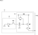
- FIG. 2 is a diagram illustrating an example of a circuit configuration of a pixel.
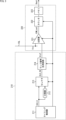
- FIG. 2 is a diagram illustrating an example of the configuration of a reference signal generating unit and an ADC.
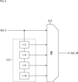
- FIG. 2 is a diagram illustrating a detailed configuration example of a frequency divider and a selector.
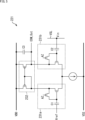
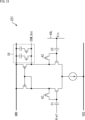
- FIG. 4 is a diagram illustrating an example of a circuit configuration of a comparator.
- FIG. 1 is a diagram illustrating an example of the configuration of a conventional ADC.
- 11 is a timing chart showing an example of the operation of a reference signal generating unit and an ADC.
- FIG. 11 is a diagram illustrating a change in analog gain. 4 is a diagram illustrating an outline of a circuit configuration example of a ramp signal generating circuit.
- FIG. 13 is a timing chart showing another example of the operation of the reference signal generating unit and the ADC.
- FIG. 13 is a diagram illustrating the relationship between the band-limiting capacity and the cutoff frequency.
- 11A and 11B are diagrams illustrating improvement in linearity due to a band-limiting capacity.
- FIG. 13 is a diagram illustrating another example of the circuit configuration of the comparator. 13 is a timing chart showing another example of the operation of the reference signal generating unit and the ADC. 13 is a timing chart showing another example of the operation of the reference signal generating unit and the ADC.
- 1 is a block diagram showing an example configuration of an electronic device to which the technology according to the present disclosure is applied.
- FIG. 1 is a diagram showing an example of a schematic configuration of a solid-state imaging device to which the technology according to the present disclosure is applied.
- the solid-state imaging device 1 shown in FIG. 1 is, for example, a camera module including a CMOS (Complementary Metal Oxide Semiconductor) image sensor and a signal processing circuit that processes signals obtained from the CMOS image sensor.
- the solid-state imaging device 1 includes a pixel array section 10 in which a plurality of pixels 11 are provided. In the pixel array section 10, the plurality of pixels 11 are arranged two-dimensionally (in a matrix).
- the pixel array section 10 has a number of pixels 11 that output pixel signals according to the amount of incident light, a number of drive wirings, and a number of data output lines VSL.
- the drive wirings are wirings to which control signals that control the output of electric charges accumulated in the pixels 11 are applied, and extend, for example, in the row direction.
- the drive wirings are connected, for example, to the output terminals of a vertical drive circuit 21, which will be described later.
- the data output lines VSL are wirings that output pixel signals output from each pixel 11 to a peripheral circuit 20, which will be described later, and extend, for example, in the column direction.
- the data output lines VSL are connected to the output terminals of a readout circuit 13, which will be described later.
- the pixel 11 is configured to include a pixel circuit 12 including a photodiode PD, and a readout circuit 13 that reads out a pixel signal from the pixel circuit 12.
- the photodiode PD is an element that performs photoelectric conversion to generate an electric charge according to the amount of incident light (amount of received light).
- the pixel circuit 12 further has a transfer transistor TRG, and by turning on the transfer transistor TRG, the electric charge stored in the photodiode PD is transferred to the readout circuit 13 (floating diffusion FD).
- the read circuit 13 includes, for example, a floating diffusion FD, a reset transistor RST, an amplification transistor AMP, and a selection transistor SEL.
- the floating diffusion FD is a floating diffusion region that temporarily holds the charge output from the photodiode PD via the transfer transistor TRG.
- a reset transistor RST is connected to the floating diffusion FD, and the data output line VSL is connected via the amplification transistor AMP and the selection transistor SEL.
- the drain of the reset transistor RST is connected to the power supply line VDD, and the source is connected to the floating diffusion FD.
- the reset transistor RST initializes (resets) the floating diffusion FD in response to a control signal applied to the gate electrode. For example, when the reset transistor RST is turned on, the potential of the floating diffusion FD is reset to the potential level of the power supply line VDD. In other words, the floating diffusion FD is initialized.
- the amplifier transistor AMP has a gate electrode connected to the floating diffusion FD and a drain connected to the power supply line VDD, and serves as the input of a source follower circuit that reads out the charge obtained by photoelectric conversion in the photodiode PD.
- the amplifier transistor AMP has a source connected to the data output line VSL via the selection transistor SEL, and thus constitutes a source follower circuit with a constant current source connected to one end of the data output line VSL.
- the selection transistor SEL is connected between the source of the amplification transistor AMP and the data output line VSL, and a control signal is supplied to the gate electrode of the selection transistor SEL as a selection signal.
- the control signal is turned on, the selection transistor SEL becomes conductive, and the pixel 11 including the conductive selection transistor SEL becomes selected.
- the pixel signal output from the amplification transistor AMP is read out to the AD (Analog to Digital) conversion circuit 22 via the data output line VSL.
- the solid-state imaging device 1 further includes a peripheral circuit 20 that processes pixel signals.
- the peripheral circuit 20 generates an image signal based on the pixel signal input from the pixel array section 10 and outputs the image signal to the outside.
- the peripheral circuit 20 includes, for example, a vertical drive circuit 21, an AD conversion circuit 22, a horizontal drive circuit 23, a system control circuit 24, and an output circuit 25.
- the vertical drive circuit 21, sequentially selects a plurality of pixels 11 for each predetermined unit pixel row.
- a "predetermined unit pixel row” refers to a pixel row that can be selected by the same address.
- the AD conversion circuit 22, for example, performs correlated double sampling (CDS) processing on the pixel signals output from each pixel 11 in the pixel row selected by the vertical drive circuit 21.
- the AD conversion circuit 22 extracts the signal level of the pixel signal by performing CDS processing, for example, and holds the pixel signal according to the amount of light received by each pixel 11.
- the AD conversion circuit 22 has an ADC, which will be described later, for each data output line VSL, for example.
- the ADC converts the analog signal (pixel signal) output for each column from the pixel array section 10 into a digital signal and outputs it. The internal configuration of the ADC will be described later.
- the horizontal drive circuit 23 is configured, for example, with a shift register, and controls the column addresses and column scanning of the multiple ADCs in the AD conversion circuit 22. Under the control of the horizontal drive circuit 23, the N-bit digital signals AD converted by each of the multiple ADCs are read out in sequence to the output circuit 25, and output as an image signal (image data) via the output circuit 25.
- the system control circuit 24 controls the driving of each block (the vertical drive circuit 21, the AD conversion circuit 22, and the horizontal drive circuit 23) in the peripheral circuit 20, for example.
- the reference signal generating unit 210 shown in FIG. 3 is, for example, included in the above-mentioned system control circuit 24.
- the reference signal generating unit 210 includes, for example, a timing control unit 211, a frequency divider 212, a selector 213, and a ramp signal generating circuit (reference signal generating circuit) 214.
- the ADC 220 shown in FIG. 3 is included in the AD conversion circuit 22 described above, and is provided for each data output line VSL.
- the ADC 220 includes, for example, a single-slope A/D converter.
- the single-slope A/D converter includes, for example, a comparator 221, a counter 222, and a memory 223.
- the timing control unit 211 functions as a clock signal generating unit that generates a clock signal, and supplies the generated clock signal CLK_0 to the frequency divider 212 and the selector 213.
- the timing control unit 211 also generates a timing signal synchronized with the clock signal CLK_0, and supplies it to the selector 213 and the ramp signal generating circuit 214, and further to the comparator 221 and the counter 222.
- the frequency divider 212 divides the frequency of the clock signal CLK_0 from the timing control unit 211.
- the divided clock signal obtained by dividing the frequency of the clock signal CLK_0 is supplied to the selector 213.
- the selector 213 switches between clock signals of different frequencies and outputs them. Specifically, the selector 213 selects either the clock signal CLK_0 or the divided clock signal from the frequency divider 212 in response to the timing signal from the timing control unit 211, and inputs it to the ramp signal generation circuit 214 as the clock signal CLK_IN.
- FIG. 4 shows a detailed example configuration of the frequency divider 212 and the selector 213.
- the divider 212 shown in FIG. 4 is composed of four divider circuits, each of which is made up of a logic circuit such as a D-type flip-flop.
- clock signal CLK_0 is divided by 2, 4, 8, and 16 to generate divided clock signals of four different frequencies, which are then supplied to the selector 213.
- the selector 213 shown in FIG. 4 is configured as a multiplexer made up of logic circuits. In the example of FIG. 4, either the clock signal CLK_0 or one of the four divided clock signals from the frequency divider 212 is selected and input to the ramp signal generating circuit 214 as the clock signal CLK_IN.
- the ramp signal generating circuit 214 generates a reference signal (ramp signal) Vref for comparison with the pixel signal for each data output line VSL.
- the ramp signal Vref has a ramp waveform with a slope that depends on the frequency of the clock signal CLK_IN. Therefore, the ramp signal generating circuit 214 generates ramp signals Vref with different slopes in response to clock signals of different frequencies input from the selector 213. For example, the ramp signal generating circuit 214 generates ramp signals with two types of slope in response to the frequency of the clock signal CLK_IN.
- the ramp signal generating circuit 214 when a clock signal of a first frequency is input from the selector 213 as the clock signal CLK_IN, the ramp signal generating circuit 214 generates a first ramp signal based on the clock signal of the first frequency.
- the ramp signal generating circuit 214 When a clock signal of a second frequency different from the first frequency is input from the selector 213 as the clock signal CLK_IN, the ramp signal generating circuit 214 generates a second ramp signal with a different slope from the first ramp signal based on the clock signal of the second frequency.
- the ramp signal Vref is input to the ramp signal Vref input terminal of the comparator 221.
- the comparator 221 compares the ramp signal Vref of a ramp waveform supplied from the ramp signal generating circuit 214 with the pixel signal Vin obtained from the pixel 11 for each row via the data output line VSL.
- the counter 222 counts the comparison time of the comparator 221.
- Memory 223 holds the count value of counter 222.
- the output of memory 223 in each ADC 220 is connected to a horizontal transfer line (not shown).
- a comparator 221 arranged for each column compares the pixel signal Vin read out to the data output line VSL with the ramp signal Vref.
- the counters 222 arranged for each column similar to the comparators 221, operate, and the ramp signal Vref and the count value change in one-to-one correspondence, thereby converting the pixel signal Vin into a digital signal.
- the data held in memory 223 is transferred to a horizontal transfer line (not shown).
- the transferred data is input to output circuit 25, and a two-dimensional image is generated by predetermined signal processing.
- the sampled pixel signal is subjected to two AD conversions, one with a high analog gain and one with a low analog gain, and the two AD conversion results are output, making it possible to select a signal with an appropriate analog gain.
- FIG. 5 shows an example of the circuit configuration of the comparator 221.
- the comparator 221 has a pipeline configuration in which the number of input capacitances, differential amplification transistors, and AZ switches is the same as the number of ramp signals input to the comparator 221.
- the comparator 221 has a differential amplifier circuit (differential pair) 231 (lamp side circuit 231a and pixel side circuit 231b) as shown in FIG. 5, for example.
- the differential amplifier circuit (differential pair) 231 (lamp side circuit 231a and pixel side circuit 231b) is an amplifier circuit that amplifies the difference between the pixel signal Vin and the ramp signal Vref of the ramp signal generation circuit 214.
- the lamp side circuit 231a includes, for example, an input capacitance C1, a differential amplification transistor, and an AZ switch.
- the pixel side circuit 231b includes, for example, an input capacitance C2, a differential amplification transistor, and an AZ switch.
- the comparator 221 has an output load circuit 232, as shown in FIG. 5.
- the output load circuit 232 is a circuit that serves as an output load for the differential amplifier circuit (differential pair) 231 (lamp side circuit 231a and pixel side circuit 231b).
- a band-limiting capacitance C3 serving as a low pass filter (LPF) is provided between the power supply line VDD and the output terminal (COM_Out).
- the solid-state imaging device of Patent Document 1 includes an ADC 320 as shown in FIG. 6.
- the solid-state imaging device of Patent Document 1 has two ramp signal generating circuits (ramp signal generating circuit 310H and ramp signal generating circuit 310L).
- the ramp signal generating circuit 310H generates a ramp signal VrefH with a relatively low slope compared to the ramp signal generating circuit 310L based on a clock signal provided by a clock signal generating unit (not shown).
- the ramp signal generating circuit 310L generates a ramp signal VrefL with a relatively high slope compared to the ramp signal generating circuit 310H based on a clock signal provided by a clock signal generating unit (not shown).
- the ADC 320 includes a comparator 321, a counter 322, and a memory 323.
- the comparator 321, the counter 322, and the memory 323 have the same configurations as the comparator 221, the counter 222, and the memory 223 described with reference to FIG. 3, respectively.
- the comparator 321 compares the ramp signals VrefH and VrefL of the ramp waveforms supplied from the two ramp signal generating circuits 310H and 310L with the pixel signal Vin obtained from the pixels 11 for each row via the data output line VSL.
- ramp signals with different analog gains can be generated by switching the frequency of the clock signal CLK_IN input to one ramp signal generating circuit 214.
- the comparator 221 it is sufficient to provide only one pair of differential pairs including an input capacitance, a differential amplification transistor, and an AZ switch, the number of which is equal to the number of ramp signals input to the comparator 221.
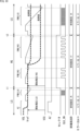
- FIG. 7 is a timing chart showing an example of the operation of the reference signal generating unit 210 and the ADC 220.
- FIG. 7 shows the waveforms of the data output line VSL (pixel signal Vin), the ramp signal Vref, the AZ switch of the comparator 221 (differential amplifier circuit 231), the selector 213, and the clock signal CLK_IN (operation timing) during one horizontal period (A/D conversion period).
- the solid-state imaging device 1 executes auto-zero (AZ) of the ADC 220.
- the ADC 220 performs AZ operation under the control of the timing control unit 211 to set the two input terminals (Vin, Vref) of the comparator 221 to the same voltage.
- the ADC 220 applies an on voltage to the AZ switch, and charges the input capacitances C1 and C2 so that the voltages applied to the two input terminals of the comparator 221 are equal to each other.
- the AZ operation is executed at a start voltage, which will be described later.
- the high frequency clock signal CLK_IN is output from the selector 213.
- the high frequency clock signal CLK_IN is equal to the clock signal CLK_0 from the timing control unit 211.
- the period during which the high-frequency clock signal CLK_IN is output is referred to as the LG (Low Gain) period
- the period during which the low-frequency clock signal CLK_IN is output is referred to as the HG (High Gain) period.
- the solid-state imaging device 1 acquires the AD conversion value (P_low) of the pixel signal Vin during the reset operation (P phase (LG)) in the LG period.
- the ADC 220 applies an off voltage to the AZ switch based on the control by the timing control unit 211.
- the ramp signal generation circuit 214 inputs the P-phase ramp signal Vref to the comparator 221.
- the P-phase pixel signal Vin output from the pixel 11 during the reset operation is provided to the data output line VSL.
- the comparator 221 acquires the P-phase ramp signal Vref and also acquires the P-phase pixel signal Vin.
- the comparator 221 When the P-phase pixel signal Vin is smaller than the P-phase ramp signal Vref, the comparator 221 outputs a comparison result signal COM_Out of H (High), and when the P-phase pixel signal Vin is larger than the P-phase ramp signal Vref, the comparator 221 outputs a comparison result signal COM_Out of L (Low).
- the comparator 221 outputs the comparison result signal COM_Out to the counter 222.
- the counter 222 counts up only while the H comparison result signal COM_Out is being supplied based on the timing signal supplied from the timing control unit 211.
- the count result becomes the AD conversion value P_low of the P phase (LG) and is stored in the memory 223. In this way, the ADC 220 acquires the AD conversion value P_low of the P phase (LG).
- the selector 213 switches, and the low-frequency clock signal CLK_IN is output from the selector 213, that is, the HG period is entered.
- the low-frequency clock signal CLK_IN is a divided clock signal obtained by dividing the clock signal CLK_0 from the timing control unit 211.
- the solid-state imaging device 1 acquires the AD conversion value (P_high) of the pixel signal Vin during the reset operation (P phase (HG)) in the HG period.
- the ADC 220 applies an off voltage to the AZ switch based on the control by the timing control unit 211.
- the ramp signal generation circuit 214 inputs the P-phase ramp signal Vref to the comparator 221.
- the P-phase pixel signal Vin output from the pixel 11 during the reset operation is provided to the data output line VSL.
- the comparator 221 acquires the P-phase ramp signal Vref and also acquires the P-phase pixel signal Vin.
- the comparator 221 When the P-phase pixel signal Vin is smaller than the P-phase ramp signal Vref, the comparator 221 outputs an H comparison result signal COM_Out, and when the P-phase pixel signal Vin is larger than the P-phase ramp signal Vref, the comparator 221 outputs an L comparison result signal COM_Out.
- the comparator 221 outputs the comparison result signal COM_Out to the counter 222.
- the counter 222 counts up only while the H comparison result signal COM_Out is being supplied based on the timing signal supplied from the timing control unit 211.
- the count result becomes the AD conversion value P_high of the P phase (HG) and is stored in the memory 223. In this way, the ADC 220 acquires the AD conversion value P_high of the P phase (HG).
- the solid-state imaging device 1 acquires the AD conversion value (D_high) of the pixel signal Vin when a signal is output during the HG period (D phase (HG)).
- the ADC 220 applies an off voltage to the AZ switch based on the control by the timing control unit 211 when outputting a signal (signal output period).
- the ramp signal generation circuit 214 inputs the D-phase ramp signal Vref to the comparator 221.
- the D-phase pixel signal Vin output from the pixel 11 when outputting a signal is provided to the data output line VSL.
- the comparator 221 acquires the D-phase ramp signal Vref and also acquires the D-phase pixel signal Vin.
- the comparator 221 When the D-phase pixel signal Vin is smaller than the D-phase ramp signal Vref, the comparator 221 outputs an H comparison result signal COM_Out, and when the D-phase pixel signal Vin is larger than the D-phase ramp signal Vref, the comparator 221 outputs an L comparison result signal COM_Out.
- the comparator 221 outputs the comparison result signal COM_Out to the counter 222.
- the counter 222 counts up only while the H comparison result signal COM_Out is being supplied based on the timing signal supplied from the timing control unit 211.
- the count result becomes the D-phase AD conversion value D_high, which is stored in the memory 223. In this way, the ADC 220 acquires the D-phase AD conversion value D_high.
- the selector 213 switches, and the high-frequency clock signal CLK_IN is again output from the selector 213, i.e., the LG period begins.
- the solid-state imaging device 1 acquires the AD conversion value (D_low) of the pixel signal Vin when a signal is output during the LG period (D phase (LG)).
- the ADC 220 applies an off voltage to the AZ switch based on the control by the timing control unit 211 when outputting a signal (signal output period).
- the ramp signal generation circuit 214 inputs the D-phase ramp signal Vref to the comparator 221.
- the D-phase pixel signal Vin output from the pixel 11 when outputting a signal is provided to the data output line VSL.
- the comparator 221 acquires the D-phase ramp signal Vref and also acquires the D-phase pixel signal Vin.
- the comparator 221 When the D-phase pixel signal Vin is smaller than the D-phase ramp signal Vref, the comparator 221 outputs an H comparison result signal COM_Out, and when the D-phase pixel signal Vin is larger than the D-phase ramp signal Vref, the comparator 221 outputs an L comparison result signal COM_Out.
- the comparator 221 outputs the comparison result signal COM_Out to the counter 222.
- the counter 222 counts up only while the H comparison result signal COM_Out is being supplied based on the timing signal supplied from the timing control unit 211.
- the count result becomes the D-phase AD conversion value D_low, which is stored in the memory 223. In this way, the ADC 220 acquires the D-phase AD conversion value D_low.
- the ADC 220 obtains the difference between the D-phase AD conversion value D_high and the P-phase AD conversion value P_high, and stores the obtained difference in the memory 223 as the gradation signal Dout_high. Furthermore, the ADC 220 obtains the difference between the D-phase AD conversion value D_low and the P-phase AD conversion value P_low, and stores the obtained difference in the memory 223 as the gradation signal Dout_low. In this way, the ADC 220 obtains the gradation signals Dout_high and Dout_low.
- the AD conversion circuit 22 reads out the gradation signals Dout_high and Dout_low from the memory 223 of each ADC 220 under the control of the horizontal drive circuit 23, and outputs them to the output circuit 25 via the horizontal transfer line.
- the output circuit 25 determines whether the gradation signal Dout_high is greater than a predetermined threshold Dth. If the gradation signal Dout_high is greater than the threshold Dth, the output circuit 25 selects and outputs the gradation signal Dout_low of the pixel row corresponding to the gradation signal Dout_high greater than the threshold Dth. On the other hand, if the gradation signal Dout_high is equal to or less than the threshold Dth, the output circuit 25 selects and outputs the gradation signal Dout_high equal to or less than the threshold Dth. In this manner, AD conversion is performed in the solid-state imaging device 1.
- the output circuit 25 may also combine the digital signals with different analog gains and output it as image data.
- the output circuit 25 can also output a digital signal that is a blend of the gradation signal Dout_high and the gradation signal Dout_low of each pixel column as an image signal.
- the starting voltage of the ramp signal Vref which is based on a reference potential VSS such as GND, is set to the same level during the LG period and the HG period.
- ramp signals VrefH and VrefL with different analog gains are input independently to a comparator, so the comparator requires two sets of input capacitance to hold the starting voltages of the ramp signals VrefH and VrefL in the LG and HG periods.
- the starting voltage of the ramp signal Vref is at the same level in the LG period and the HG period, so even if the analog gains are different, the operating point of the comparator 221 does not change and only one AZ operation is required. In other words, only one set of input capacitances is required to hold the starting voltage of the ramp signal Vref.
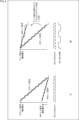
- Figure 8A shows an example of changing the analog gain (slope of the ramp signal) between the LG period and the HG period using conventional technology.
- Figure 8A shows a ramp signal (LG ramp signal) with a low analog gain (large slope) and a ramp signal (HG ramp signal) with a high analog gain (small slope) that are generated according to the default clock signal CLK_0.
- FIG. 8B shows an example of changing the analog gain (slope of the ramp signal) between the LG period and the HG period using the technology disclosed herein.
- a ramp signal (LG ramp signal) with low analog gain (large slope) generated according to the default clock signal CLK_0, and a ramp signal (HG ramp signal) with high analog gain (small slope) generated according to the clock signal CLK_IN obtained by dividing the clock signal CLK_0 by 4 are shown.
- the analog gain (slope of the ramp signal) can be changed between the LG period and the HG period based on clock signals with different division ratios (frequencies). Specifically, by dividing the clock signal, the time of one clock is extended, and the slope of the ramp signal becomes gentler, resulting in a change in the analog gain (to four times (+12 dB) in the example of Figure B).
- the analog gain can be changed by changing the time axis direction of the clock signal between the LG period and the HG period. This makes it possible to make the starting voltage of the ramp signal the same level between the LG period and the HG period.
- a frequency divider 212 and a selector 213 are newly provided as a configuration for outputting clock signals with different division ratios (frequencies). Since the frequency divider 212 and the selector 213 are both made up of logic circuits, even if the frequency divider 212 and the selector 213 are newly provided, the circuit area can be kept small. Therefore, it is possible to realize a configuration that changes the analog gain while suppressing an increase in the circuit area.
- the above operation makes it possible for the solid-state imaging device 1 to perform AD conversion on sampled pixel signals with different analog gains while suppressing increases in the circuit area and power consumption of the ramp signal generation circuit and comparator. As a result, even when the subject contains a mixture of high-illumination and low-illumination areas, it is possible to expand the dynamic range by selecting a signal with an appropriate analog gain.
- FIG. 9 is a diagram showing an outline of an example of the circuit configuration of the ramp signal generating circuit 214. As shown in FIG.
- the ramp signal generating circuit 214 shown in FIG. 9 is configured to include a current mirror circuit CMR formed from a transistor that serves as a current source on the reference current side and a transistor that serves as a current source on the output current side.
- the magnitude of noise and the magnitude of power consumption can be adjusted by adjusting the termination resistance R and the current mirror ratio m/n. Specifically, by reducing the termination resistance R, the noise can be reduced, and by reducing the current mirror ratio m/n, the power consumption can be reduced.
- the starting voltage of the ramp signal Vref must be at the same level during the LG period and the HG period.
- the ramp signal generating circuit 214 adjusts the termination resistor R that determines the ramp signal Vref and the current mirror ratio m/n (the output current m/n x Iref that flows through the termination resistor R) so that the starting voltage of the ramp signal Vref is constant between the LG period and the HG period.
- the level of noise there is a trade-off between the level of noise and the level of power consumption.
- the termination resistance R is made small, the noise can be reduced, but the current mirror ratio m/n must be made large, which increases the power consumption.
- the current mirror ratio m/n is made small, the power consumption can be reduced, but the termination resistance R must be made large, which increases the noise.
- the termination resistance R and the current mirror ratio m/n may be adjusted according to the timing of switching between the LG period and the HG period based on the control by the timing control unit 211.
- the ramp signal generating circuit 214 may adjust the termination resistance R and the current mirror ratio m/n in conjunction with the operation of the selector 213, i.e., in response to switching of the frequency of the clock signal, while keeping the ratio of the termination resistance R and the current mirror ratio m/n (output current) constant.
- the current mirror ratio m/n is made small while the termination resistance R is made large, so that the ratio between the termination resistance R and the current mirror ratio m/n is kept constant. In this case, the noise increases, but the power consumption can be reduced.
- the termination resistance R is reduced while the current mirror ratio m/n is increased, so that the ratio between the termination resistance R and the current mirror ratio m/n is kept constant. In this case, power consumption increases, but noise can be reduced.
- a band-limiting capacitance serving as an LPF is provided between the power supply line VDD and the output terminal (COM_Out).
- Figure 11 shows the relationship between the bandwidth limiting capacity and the cutoff frequency.
- the linearity of the ramp signal input to the comparator 221 deteriorates.
- the linearity of the ramp signal can be improved by increasing the band limiting capacity (lowering the cutoff frequency) in the comparator 221.
- the bandwidth limiting capacitance provided in the comparator 221 may be a bandwidth limiting capacitance CV (variable capacitance) whose capacitance value can be changed.
- the capacitance value of the bandwidth limiting capacitance CV may be adjusted in accordance with the timing of switching between the LG period and the HG period based on the control by the timing control unit 211.
- the comparator 221 may change the capacitance value of the band-limiting capacitance CV in conjunction with the operation of the selector 213, that is, in response to switching of the frequency of the clock signal.
- the ramp signal generating circuit 214 may generate ramp signals having three different slopes according to the frequency of the clock signal CLK_IN.
- the ramp signal generating circuit 214 when a clock signal of a first frequency is input from the selector 213 as the clock signal CLK_IN, the ramp signal generating circuit 214 generates a first ramp signal based on the clock signal of the first frequency.
- the ramp signal generating circuit 214 When a clock signal of a second frequency different from the first frequency is input from the selector 213 as the clock signal CLK_IN, the ramp signal generating circuit 214 generates a second ramp signal with a different slope from the first ramp signal based on the clock signal of the second frequency.
- the ramp signal generating circuit 214 when a clock signal of a third frequency different from the first and second frequencies is input from the selector 213 as the clock signal CLK_IN, the ramp signal generating circuit 214 generates a third ramp signal with a different slope from the first and second ramp signals based on the clock signal of the third frequency.
- the solid-state imaging device 1 After performing the AZ operation, the solid-state imaging device 1 performs a reset operation (P phase (LG)) during the LG period in which the high-frequency clock signal CLK_IN is output.
- P phase (LG) P phase
- the selector 213 switches, and a transition occurs to the MG period in which the clock signal CLK_IN with a mid-frequency range is output.
- the solid-state imaging device 1 performs a reset operation (P phase (MG)) in the MG period.
- the selector 213 switches, and a transition occurs to the HG period in which the low-frequency clock signal CLK_IN is output.
- the solid-state imaging device 1 performs a reset operation (P phase (HG)) and a signal output (D phase (HG)) in the HG period.
- the selector 213 switches, and the MG period begins again, during which the clock signal CLK_IN with a mid-frequency range is output.
- the solid-state imaging device 1 performs signal output (D phase (MG)) during the MG period.
- the selector 213 switches, and the LG period begins again, during which the high-frequency clock signal CLK_IN is output.
- the solid-state imaging device 1 performs signal output (D phase (LG)) during the LG period.
- the above operation makes it possible to select an appropriate analog gain signal when the subject contains a mixture of high, medium, and low illumination areas, with a configuration that minimizes increases in the circuit area and power consumption of the ramp signal generation circuit and comparator.
- the ramp signal generating circuit 214 can generate ramp signals with multiple types of slopes depending on the frequency of the clock signal CLK_IN.
- the technology according to the present disclosure is not limited to application to solid-state imaging devices. That is, the technology according to the present disclosure is applicable to imaging devices such as digital still cameras and video cameras, portable terminal devices having imaging functions, copiers using solid-state imaging devices in image reading units, and other electronic devices that use solid-state imaging devices in image capture units (photoelectric conversion units).
- the solid-state imaging device may be formed as a single chip, or may be in the form of a module having an imaging function in which an imaging unit and a signal processing unit or an optical system are packaged together.
- FIG. 16 is a block diagram showing an example of the configuration of an imaging device as an electronic device to which the technology disclosed herein is applied.
- the imaging device 500 in FIG. 16 comprises an optical section 501 consisting of a group of lenses etc., a solid-state imaging device (imaging device) 502 employing the configuration of the solid-state imaging device 1 in FIG. 1, and a DSP (Digital Signal Processor) circuit 503 which is a camera signal processing circuit.
- the imaging device 500 also comprises a frame memory 504, a display section 505, a recording section 506, an operation section 507, and a power supply section 508.
- the DSP circuit 503, frame memory 504, display section 505, recording section 506, operation section 507, and power supply section 508 are interconnected via a bus line 509.
- the optical unit 501 takes in incident light (image light) from a subject and forms an image on the imaging surface of the solid-state imaging device 502.
- the solid-state imaging device 502 converts the amount of incident light formed on the imaging surface by the optical unit 501 into an electrical signal on a pixel-by-pixel basis and outputs it as a pixel signal.
- the solid-state imaging device 1 of FIG. 1 that is, a solid-state imaging device that changes analog gain (slope of a ramp signal) based on clock signals with different division ratios (frequencies), can be used.
- the display unit 505 is formed of a thin display such as an LCD (Liquid Crystal Display) or an organic EL (Electro Luminescence) display, and displays moving images or still images captured by the solid-state imaging device 502.
- the recording unit 506 records the moving images or still images captured by the solid-state imaging device 502 on a recording medium such as a hard disk or semiconductor memory.
- Operation unit 507 issues operation commands for various functions of imaging device 500 under the operation of a user.
- Power supply unit 508 appropriately supplies various types of power to these devices as operating power sources for DSP circuit 503, frame memory 504, display unit 505, recording unit 506, and operation unit 507.
- the solid-state imaging device 1 As described above, by using the solid-state imaging device 1 to which the above-mentioned embodiment is applied as the solid-state imaging device 502, it is possible to suppress an increase in the circuit area and power consumption of the ramp signal generating circuit and comparator in the solid-state imaging device 502. Therefore, it is possible to reduce the size of the device and the power consumption in imaging devices 500 such as video cameras, digital still cameras, and even camera modules for mobile devices such as mobile phones.
- the technology disclosed herein can be applied to light detection devices in general, including not only solid-state imaging devices as image sensors described above, but also distance measurement sensors that measure distance, also known as ToF (Time of Flight) sensors.
- a distance measurement sensor emits light toward an object, detects the light that is reflected back from the surface of the object, and calculates the distance to the object based on the flight time from when the light is emitted until the reflected light is received.
- the technology according to the present disclosure can have the following configuration.
- a pixel array unit having a plurality of pixels that output pixel signals corresponding to the amount of incident light;
- a reference signal generating unit that generates a reference signal;
- a comparator provided for each pixel column, the comparator comparing the pixel signal with the reference signal;
- the reference signal generation unit a clock signal generating unit that generates a clock signal; a frequency divider for dividing the frequency of the clock signal; a selector for switching between and outputting the clock signals having different frequencies; a reference signal generating circuit that generates the reference signal having a different slope in accordance with the frequency of the clock signal.
- the reference signal generating circuit includes: generating a first reference signal based on the clock signal at a first frequency;
- the photodetection device according to any one of claims 1 to 5, further comprising: a clock signal having a second frequency, the clock signal being supplied to the first reference signal source, the clock signal being supplied to the second reference signal source, and a clock signal having a second frequency.
- the reference signal generating circuit includes: The photodetection device according to (2), further comprising: a third reference signal having a slope different from the slopes of the first reference signal and the second reference signal, based on the clock signal having a third frequency.
- an AD conversion circuit including the comparator, the AD conversion circuit performing AD (Analog to Digital) conversion of the pixel signal based on a comparison result between the reference signal having a different slope and the pixel signal, thereby outputting a different digital signal;
- the light detection device according to any one of (1) to (8), further comprising: an output circuit that selects one of the digital signals and outputs it as image data.
- the photodetector according to claim 9, wherein the output circuit selects one of the digital signals based on a predetermined threshold value.
- an AD conversion circuit including the comparator, the AD conversion circuit performing AD (Analog to Digital) conversion of the pixel signal based on a comparison result between the reference signal having a different slope and the pixel signal, thereby outputting a different digital signal;
- the light detection device according to any one of (1) to (8), further comprising: an output circuit that combines the different digital signals and outputs the combined signal as image data.
- a pixel array unit having a plurality of pixels that output pixel signals corresponding to the amount of incident light;
- a reference signal generating unit that generates a reference signal;
- a comparator provided for each pixel column, the comparator comparing the pixel signal with the reference signal;
- the reference signal generation unit a clock signal generating unit that generates a clock signal; a frequency divider for dividing the frequency of the clock signal; a selector for switching between and outputting the clock signals having different frequencies; and a reference signal generating circuit that generates the reference signal with a different slope depending on the frequency of the clock signal.
- 1 solid-state imaging device 10 pixel array section, 11 pixel, 20 peripheral circuit, 21 vertical drive circuit, 22 AD conversion circuit, 23 horizontal drive circuit, 24 system control circuit, 25 output circuit, 210 reference signal generation section, 211 timing control section, 212 frequency divider, 213 selector, 214 ramp signal generation circuit, 220 ADC, 221 comparator, 222 counter, 223 memory, C1, C2 input capacitance, C3 band limiting capacitance, CMR current mirror circuit, CV band limiting capacitance
Landscapes
- Engineering & Computer Science (AREA)
- Multimedia (AREA)
- Signal Processing (AREA)
- Transforming Light Signals Into Electric Signals (AREA)
Abstract
本開示は、回路面積と消費電力の増大を抑えることができるようにする光検出装置および電子機器に関する。 光検出装置は、入射光量に応じた画素信号を出力する複数の画素を有する画素アレイ部と、参照信号を生成する参照信号生成部と、画素列に設けられた、画素信号と参照信号とを比較する比較器とを備える。参照信号生成部は、クロック信号を生成するクロック信号生成部と、クロック信号を分周する分周器と、異なる周波数のクロック信号を切り替えて出力するセレクタと、クロック信号の周波数に応じて、異なる傾きの参照信号を生成する参照信号生成回路とを有する。本開示に係る技術は、例えば、CMOSイメージセンサに適用することができる。
Description
本開示は、光検出装置および電子機器に関し、特に、回路面積と消費電力の増大を抑えることができるようにする光検出装置および電子機器に関する。
被写体に高照度領域と低照度領域が混在している場合、低照度領域におけるS/Nを確保しつつ、ダイナミックレンジを拡大するためには、それぞれの領域に適したアナログゲインで読み出しを行う必要があった。
これに対して、特許文献1には、サンプリングされた画素信号に対して、高いアナログゲインと低いアナログゲインで2回のAD変換を行い、2つのAD変換結果を出力することで、適切なアナログゲインの信号を選択できるようにした固体撮像装置が開示されている。
しかしながら、特許文献1の固体撮像装置においては、異なるアナログゲイン(傾き)のランプ信号を生成するために2つのランプ信号生成回路を設ける必要があった。また、異なるアナログゲインのランプ信号が入力される比較器においては、入力容量、差動増幅トランジスタ、AZ(Auto Zero)スイッチを含む差動対を2組備える必要があった。そのため、回路面積と消費電力の増大が課題となっていた。
本開示は、このような状況に鑑みてなされたものであり、回路面積と消費電力の増大を抑えることができるようにするものである。
本開示の光検出装置は、入射光量に応じた画素信号を出力する複数の画素を有する画素アレイ部と、参照信号を生成する参照信号生成部と、画素列毎に設けられた、前記画素信号と前記参照信号とを比較する比較器とを備え、前記参照信号生成部は、クロック信号を生成するクロック信号生成部と、前記クロック信号を分周する分周器と、異なる周波数の前記クロック信号を切り替えて出力するセレクタと、前記クロック信号の周波数に応じて、異なる傾きの前記参照信号を生成する参照信号生成回路とを有する光検出装置である。
本開示の電子機器は、入射光量に応じた画素信号を出力する複数の画素を有する画素アレイ部と、参照信号を生成する参照信号生成部と、画素列毎に設けられた、前記画素信号と前記参照信号とを比較する比較器とを備え、前記参照信号生成部は、クロック信号を生成するクロック信号生成部と、前記クロック信号を分周する分周器と、異なる周波数の前記クロック信号を切り替えて出力するセレクタと、前記クロック信号の周波数に応じて、異なる傾きの前記参照信号を生成する参照信号生成回路とを有する光検出装置を備える電子機器である。
本開示においては、光検出装置に、入射光量に応じた画素信号を出力する複数の画素を有する画素アレイ部と、参照信号を生成する参照信号生成部と、画素列毎に設けられた、前記画素信号と前記参照信号とを比較する比較器とが備えられ、前記参照信号生成部には、クロック信号を生成するクロック信号生成部と、前記クロック信号を分周する分周器と、異なる周波数の前記クロック信号を切り替えて出力するセレクタと、前記クロック信号の周波数に応じて、異なる傾きの前記参照信号を生成する参照信号生成回路とが設けられる。
以下、本開示を実施するための形態(以下、実施の形態とする)について説明する。なお、説明は以下の順序で行う。
1.固体撮像装置の概要
2.参照信号生成部とADCの構成例
3.固体撮像装置の動作
4.終端抵抗と出力電流の調整
5.帯域制限容量によるリニアリティの改善
6.変形例
7.電子機器の構成例
2.参照信号生成部とADCの構成例
3.固体撮像装置の動作
4.終端抵抗と出力電流の調整
5.帯域制限容量によるリニアリティの改善
6.変形例
7.電子機器の構成例
<1.固体撮像装置の概要>
図1は、本開示に係る技術を適用した固体撮像装置の概略構成例を示す図である。
図1は、本開示に係る技術を適用した固体撮像装置の概略構成例を示す図である。
図1に示される固体撮像装置1は、例えば、CMOS(Complementary Metal Oxide Semiconductor)イメージセンサと、CMOSイメージセンサから得られた信号を処理する信号処理回路とを備えたカメラモジュールである。固体撮像装置1は、複数の画素11が設けられた画素アレイ部10を備えている。画素アレイ部10において、複数の画素11は、2次元(行列状に)配置されている。
画素アレイ部10は、入射光量に応じた画素信号を出力する複数の画素11、複数の駆動配線、および複数のデータ出力線VSLを有している。駆動配線は、画素11に蓄積された電荷の出力を制御する制御信号が印加される配線であり、例えば、行方向に延在している。複数の駆動配線は、例えば、後述する垂直駆動回路21の出力端に接続されている。データ出力線VSLは、各画素11から出力された画素信号を、後述する周辺回路20に出力する配線であり、例えば、列方向に延在している。データ出力線VSLは、後述する読み出し回路13の出力端に接続されている。
画素11は、例えば図2に示されるように、フォトダイオードPDを含む画素回路12と、画素回路12から画素信号を読み出す読み出し回路13とを含んで構成されている。フォトダイオードPDは、光電変換を行って入射光量(受光量)に応じた電荷を発生する素子である。画素回路12は、さらに、転送トランジスタTRGを有しており、転送トランジスタTRGをオンすることにより、フォトダイオードPDに蓄えられた電荷を読み出し回路13(フローティングディフュージョンFD)に転送する。
読み出し回路13は、例えば、フローティングディフュージョンFD、リセットトランジスタRST、増幅トランジスタAMP、および選択トランジスタSELとを有している。
フローティングディフュージョンFDは、転送トランジスタTRGを介してフォトダイオードPDから出力された電荷を一時的に保持する浮遊拡散領域である。フローティングディフュージョンFDには、例えば、リセットトランジスタRSTが接続されるとともに、増幅トランジスタAMPと選択トランジスタSELを介してデータ出力線VSLが接続されている。
リセットトランジスタRSTでは、ドレインが電源線VDDに接続され、ソースがフローティングディフュージョンFDに接続されている。リセットトランジスタRSTは、ゲート電極に印加される制御信号に応じて、フローティングディフュージョンFDを初期化(リセット)する。例えば、リセットトランジスタRSTがオンされると、フローティングディフュージョンFDの電位が電源線VDDの電位レベルにリセットされる。すなわち、フローティングディフュージョンFDの初期化が行われる。
増幅トランジスタAMPは、ゲート電極がフローティングディフュージョンFDに接続され、ドレインが電源線VDDに接続されており、フォトダイオードPDでの光電変換によって得られる電荷を読み出すソースフォロワ回路の入力部となる。すなわち、増幅トランジスタAMPは、ソースが選択トランジスタSELを介してデータ出力線VSLに接続されることにより、データ出力線VSLの一端に接続される定電流源とソースフォロワ回路を構成する。
選択トランジスタSELは、増幅トランジスタAMPのソースとデータ出力線VSLの間に接続されており、選択トランジスタSELのゲート電極には、選択信号として制御信号が供給される。選択トランジスタSELは、制御信号がオンすると導通状態となり、導通状態となった選択トランジスタSELを含む画素11が選択状態となる。画素11が選択状態になると、増幅トランジスタAMPから出力される画素信号がデータ出力線VSLを介してAD(Analog to Digital)変換回路22に読み出される。
固体撮像装置1は、さらに、画素信号を処理する周辺回路20を備えている。周辺回路20は、画素アレイ部10から入力された画素信号に基づいて画像信号を生成し、外部に出力する。周辺回路20は、例えば、垂直駆動回路21、AD変換回路22、水平駆動回路23、システム制御回路24、および出力回路25を有している。
垂直駆動回路21は、例えば、複数の画素11を所定の単位画素行毎に順に選択する。「所定の単位画素行」とは、同一アドレスで選択可能な画素行を指している。AD変換回路22は、例えば、垂直駆動回路21によって選択された画素行の各画素11から出力される画素信号に対して、相関二重サンプリング(Correlated Double Sampling:CDS)処理を施す。AD変換回路22は、例えば、CDS処理を施すことにより、画素信号の信号レベルを抽出し、各画素11の受光量に応じた画素信号を保持する。AD変換回路22は、例えば、データ出力線VSL毎に、後述するADCを有している。ADCは、画素アレイ部10から列毎に出力されるアナログ信号(画素信号)をデジタル信号に変換して出力する。ADCの内部構成については後述するものとする。
水平駆動回路23は、例えば、シフトレジスタなどによって構成され、AD変換回路22における複数のADCの列アドレスや列走査の制御を行う。水平駆動回路23による制御の下、複数のADCの各々でAD変換されたNビットのデジタル信号が順に出力回路25に読み出され、出力回路25を経由して画像信号(画像データ)として出力される。システム制御回路24は、例えば、周辺回路20内の各ブロック(垂直駆動回路21、AD変換回路22、および水平駆動回路23)の駆動を制御する。
<2.参照信号生成部とADCの構成例>
次に、図3を参照して、参照信号生成部とADCの構成例について説明する。
次に、図3を参照して、参照信号生成部とADCの構成例について説明する。
図3に示される参照信号生成部210は、例えば、上述したシステム制御回路24に含まれる。参照信号生成部210は、例えば、タイミング制御部211、分周器212、セレクタ213、およびランプ信号生成回路(参照信号生成回路)214を含んで構成される。
図3に示されるADC220は、上述したAD変換回路22に含まれ、データ出力線VSL毎に設けられる。ADC220は、例えば、シングルスロープA/D変換器を含んでいる。シングルスロープA/D変換器は、例えば、比較器221、カウンタ222、およびメモリ223を含んで構成される。
タイミング制御部211は、クロック信号を生成するクロック信号生成部として機能し、生成したクロック信号CLK_0を分周器212とセレクタ213に供給する。また、タイミング制御部211は、クロック信号CLK_0に同期したタイミング信号を生成し、セレクタ213とランプ信号生成回路214、さらに、比較器221とカウンタ222に供給する。
分周器212は、タイミング制御部211からのクロック信号CLK_0を分周する。クロック信号CLK_0が分周された分周クロック信号は、セレクタ213に供給される。
セレクタ213は、異なる周波数のクロック信号を切り替えて出力する。具体的には、セレクタ213は、タイミング制御部211からのタイミング信号に応じて、クロック信号CLK_0と、分周器212からの分周クロック信号のいずれかを選択し、クロック信号CLK_INとして、ランプ信号生成回路214に入力する。
図4は、分周器212とセレクタ213の詳細な構成例を示す図である。
図4に示される分周器212は、それぞれD型フリップフロップなどの論理回路からなる、4つの分周回路から構成される。図4の例では、クロック信号CLK_0を2分周、4分周、8分周、16分周した4種類の周波数の分周クロック信号が生成され、セレクタ213に供給される。
図4に示されるセレクタ213は、論理回路からなるマルチプレクサとして構成される。図4の例では、クロック信号CLK_0、または、分周器212からの4種類の周波数の分周クロック信号のいずれかが選択され、クロック信号CLK_INとして、ランプ信号生成回路214に入力される。
図3に戻り、ランプ信号生成回路214は、データ出力線VSL毎の画素信号と比較するための参照信号(ランプ信号)Vrefを生成する。ランプ信号Vrefは、クロック信号CLK_INの周波数に応じた傾き(スロープ)のランプ波形を有する。したがって、ランプ信号生成回路214は、セレクタ213から入力される異なる周波数のクロック信号に応じて、異なる傾きのランプ信号Vrefを生成する。例えば、ランプ信号生成回路214は、クロック信号CLK_INの周波数に応じて、2種類の傾きを有するランプ信号を生成する。
具体的には、クロック信号CLK_INとして、セレクタ213から第1の周波数のクロック信号が入力された場合、ランプ信号生成回路214は、第1の周波数のクロック信号に基づいて、第1のランプ信号を生成する。クロック信号CLK_INとして、セレクタ213から第1の周波数とは異なる第2の周波数のクロック信号が入力された場合、ランプ信号生成回路214は、第2の周波数のクロック信号に基づいて、第1のランプ信号とは異なる傾きの第2のランプ信号を生成する。
ランプ信号Vrefは、比較器221におけるランプ信号Vrefの入力端子に入力される。
比較器221は、ランプ信号生成回路214から供給されるランプ波形のランプ信号Vrefと、行毎に画素11からデータ出力線VSLを介して得られる画素信号Vinとを比較する。
カウンタ222は、比較器221の比較時間をカウントする。
メモリ223は、カウンタ222のカウント値を保持する。各ADC220におけるメモリ223の出力は、図示せぬ水平転送線に接続される。
各ADC220において、列毎に配置された比較器221は、データ出力線VSLに読み出された画素信号Vinとランプ信号Vrefとを比較する。
このとき、比較器221と同様に列毎に配置されたカウンタ222が動作し、ランプ信号Vrefとカウント値が一対一の対応を取りながら変化することで、画素信号Vinがデジタル信号に変換される。
そして、画素信号Vinとランプ信号Vrefが交わったとき、比較器221の出力が反転するとともに、カウンタ222の入力クロックが停止し、または、入力が停止していたクロックがカウンタ222に入力され、AD変換が完了する。
AD変換期間終了後、メモリ223に保持されたデータが、図示せぬ水平転送線に転送される。転送されたデータは、出力回路25に入力され、所定の信号処理により2次元画像が生成される。
以上のような構成により、サンプリングされた画素信号に対して、高いアナログゲインと低いアナログゲインで2回のAD変換を行い、2つのAD変換結果を出力することで、適切なアナログゲインの信号を選択することが可能となる。
図5は、比較器221の回路構成例を示す図である。
比較器221は、入力容量、差動増幅トランジスタ、およびAZスイッチを、比較器221に入力されるランプ信号の数だけ設けたパイプライン構成を採る。比較器221は、例えば、図5に示されるように、差動増幅回路(差動対)231(ランプ側回路231aと画素側回路231b)を有している。差動増幅回路(差動対)231(ランプ側回路231aと画素側回路231b)は、画素信号Vinと、ランプ信号生成回路214のランプ信号Vrefとの差分を増幅する増幅回路である。
ランプ側回路231aは、例えば、入力容量C1、差動増幅トランジスタ、およびAZスイッチを含んで構成される。画素側回路231bは、例えば、入力容量C2、差動増幅トランジスタ、およびAZスイッチを含んで構成される。
さらに、比較器221は、図5に示されるように、出力負荷回路232を有している。出力負荷回路232は、差動増幅回路(差動対)231(ランプ側回路231aと画素側回路231b)の出力負荷となる回路である。
なお、比較器221において、電源線VDDと出力端子(COM_Out)との間には、LPF(Low Pass Filter)としての帯域制限容量C3が設けられる。
ここで、図6を参照して、サンプリングされた画素信号に対して、高いアナログゲインと低いアナログゲインで2回のAD変換を行うようにした、従来のADCの構成例について説明する。例えば、特許文献1の固体撮像装置は、図6に示されるようなADC320を備える。
特許文献1の固体撮像装置は、2つのランプ信号生成回路(ランプ信号生成回路310Hとランプ信号生成回路310L)を有している。
ランプ信号生成回路310Hは、図示せぬクロック信号生成部から与えられるクロック信号に基づいて、ランプ信号生成回路310Lと比べて相対的に低スロープのランプ信号VrefHを生成する。ランプ信号生成回路310Lは、図示せぬクロック信号生成部から与えられるクロック信号に基づいて、ランプ信号生成回路310Hと比べて相対的に高スロープのランプ信号VrefLを生成する。
ADC320は、比較器321、カウンタ322、およびメモリ323を含んで構成される。比較器321、カウンタ322、およびメモリ323は、それぞれ、図3を参照して説明した比較器221、カウンタ222、およびメモリ223と同様の構成を有する。
但し、比較器321は、2つのランプ信号生成回路310H,310Lから供給されるランプ波形のランプ信号VrefH,VrefLと、行毎に画素11からデータ出力線VSLを介して得られる画素信号Vinとを比較する。
このように、特許文献1の固体撮像装置においては、異なるアナログゲイン(傾き)のランプ信号を生成するために2つのランプ信号生成回路310H,310Lを設ける必要があった。また、異なるアナログゲインのランプ信号VrefH,VrefLが入力される比較器321においては、入力容量、差動増幅トランジスタ、AZスイッチを含む差動対を、比較器321に入力されるランプ信号の数、すなわち2組備える必要があった。そのため、回路面積と消費電力の増大が課題となっていた。
一方で、本開示に係る技術を適用した固体撮像装置1においては、1つのランプ信号生成回路214に入力されるクロック信号CLK_INの周波数を切り替えることによって、異なるアナログゲイン(傾き)のランプ信号を生成することができる。また、比較器221においては、入力容量、差動増幅トランジスタ、AZスイッチを含む差動対が、比較器221に入力されるランプ信号の数、すなわち1組だけ設けられればよい。
すなわち、本開示に係る技術を適用した固体撮像装置1においては、特許文献1の固体撮像装置と比較して、回路面積と消費電力の増大を抑えることが可能となる。
<3.固体撮像装置の動作>
本開示に係る技術を適用した固体撮像装置1の動作について説明する。
本開示に係る技術を適用した固体撮像装置1の動作について説明する。
図7は、参照信号生成部210とADC220の動作例を示すタイミングチャートである。
図7には、1水平期間(AD変換期間)における、データ出力線VSL(画素信号Vin)、ランプ信号Vrefの波形、比較器221(差動増幅回路231)のAZスイッチ、セレクタ213、およびクロック信号CLK_INの波形(動作タイミング)が示されている。
まず、固体撮像装置1は、ADC220のオートゼロ(AZ)を実行する。具体的には、ADC220は、タイミング制御部211による制御に基づいて、比較器221の2つの入力端子(Vin,Vref)を同電圧とするAZ動作を行う。ADC220は、例えば、タイミング制御部211による制御に基づいて、AZスイッチにオン電圧を印加し、比較器221の2つの入力端子に与えられる電圧が互いに等しくなるように、入力容量C1,C2をチャージする。なお、AZ動作は、後述する開始電圧にて実行される。
AZ動作の後、セレクタ213から高周波数のクロック信号CLK_INが出力される。ここでは、例えば、高波数のクロック信号CLK_INは、タイミング制御部211からのクロック信号CLK_0と等しい。
なお、本開示に係る技術を適用した固体撮像装置1においては、高周波数のクロック信号CLK_INがランプ信号生成回路214に入力された場合、低いアナログゲイン(大きい傾き)のランプ信号が生成され、低周波数のクロック信号CLK_INがランプ信号生成回路214に入力された場合、高いアナログゲイン(小さい傾き)のランプ信号が生成される。
そこで、以下においては、高周波数のクロック信号CLK_INが出力される期間を、LG(Low Gain)期間といい、低周波数のクロック信号CLK_INが出力される期間を、HG(High Gain)期間という。
次に、固体撮像装置1は、LG期間でのリセット動作時(P相(LG))の画素信号VinのAD変換値(P_low)を取得する。
具体的には、ADC220は、リセット動作時(リセット期間)において、タイミング制御部211による制御に基づいて、AZスイッチにオフ電圧を印加する。続いて、ランプ信号生成回路214は、P相のランプ信号Vrefを比較器221に入力する。このとき、データ出力線VSLには、リセット動作時に画素11から出力されたP相の画素信号Vinが与えられている。これにより、比較器221は、P相のランプ信号Vrefを取得するとともに、P相の画素信号Vinを取得する。比較器221は、P相の画素信号VinがP相のランプ信号Vrefよりも小さい場合に、H(High)の比較結果信号COM_Outを出力し、P相の画素信号VinがP相のランプ信号Vrefよりも大きい場合に、L(Low)の比較結果信号COM_Outを出力する。比較器221は、比較結果信号COM_Outをカウンタ222に出力する。カウンタ222は、タイミング制御部211から供給されるタイミング信号に基づいて、Hの比較結果信号COM_Outが供給されている間だけ、カウントアップする。カウント結果が、P相(LG)のAD変換値P_lowとなり、メモリ223に格納される。このようにして、ADC220は、P相(LG)のAD変換値P_lowを取得する。
その後、時刻t1において、セレクタ213が切り替わることで、セレクタ213から低周波数のクロック信号CLK_INが出力された状態、すなわち、HG期間となる。ここでは、例えば、低周波数のクロック信号CLK_INは、タイミング制御部211からのクロック信号CLK_0が分周された分周クロック信号とされる。
次に、固体撮像装置1は、HG期間でのリセット動作時(P相(HG))の画素信号VinのAD変換値(P_high)を取得する。
具体的には、ADC220は、リセット動作時(リセット期間)において、タイミング制御部211による制御に基づいて、AZスイッチにオフ電圧を印加する。続いて、ランプ信号生成回路214は、P相のランプ信号Vrefを比較器221に入力する。このとき、データ出力線VSLには、リセット動作時に画素11から出力されたP相の画素信号Vinが与えられている。これにより、比較器221は、P相のランプ信号Vrefを取得するとともに、P相の画素信号Vinを取得する。比較器221は、P相の画素信号VinがP相のランプ信号Vrefよりも小さい場合に、Hの比較結果信号COM_Outを出力し、P相の画素信号VinがP相のランプ信号Vrefよりも大きい場合に、Lの比較結果信号COM_Outを出力する。比較器221は、比較結果信号COM_Outをカウンタ222に出力する。カウンタ222は、タイミング制御部211から供給されるタイミング信号に基づいて、Hの比較結果信号COM_Outが供給されている間だけ、カウントアップする。カウント結果が、P相(HG)のAD変換値P_highとなり、メモリ223に格納される。このようにして、ADC220は、P相(HG)のAD変換値P_highを取得する。
続いて、固体撮像装置1は、HG期間での信号出力時(D相(HG))の画素信号VinのAD変換値(D_high)を取得する。
具体的には、ADC220は、信号出力時(信号出力期間)において、タイミング制御部211による制御に基づいて、AZスイッチにオフ電圧を印加する。続いて、ランプ信号生成回路214は、D相のランプ信号Vrefを比較器221に入力する。このとき、データ出力線VSLには、信号出力時に画素11から出力されたD相の画素信号Vinが与えられている。これにより、比較器221は、D相のランプ信号Vrefを取得するとともに、D相の画素信号Vinを取得する。比較器221は、D相の画素信号VinがD相のランプ信号Vrefよりも小さい場合に、Hの比較結果信号COM_Outを出力し、D相の画素信号VinがD相のランプ信号Vrefよりも大きい場合に、Lの比較結果信号COM_Outを出力する。比較器221は、比較結果信号COM_Outをカウンタ222に出力する。カウンタ222は、タイミング制御部211から供給されるタイミング信号に基づいて、Hの比較結果信号COM_Outが供給されている間だけ、カウントアップする。カウント結果が、D相のAD変換値D_highとなり、メモリ223に格納される。このようにして、ADC220は、D相のAD変換値D_highを取得する。
その後、時刻t2において、セレクタ213が切り替わることで、再び、セレクタ213から高周波数のクロック信号CLK_INが出力された状態、すなわち、LG期間となる。
固体撮像装置1は、LG期間での信号出力時(D相(LG))の画素信号VinのAD変換値(D_low)を取得する。
具体的には、ADC220は、信号出力時(信号出力期間)において、タイミング制御部211による制御に基づいて、AZスイッチにオフ電圧を印加する。続いて、ランプ信号生成回路214は、D相のランプ信号Vrefを比較器221に入力する。このとき、データ出力線VSLには、信号出力時に画素11から出力されたD相の画素信号Vinが与えられている。これにより、比較器221は、D相のランプ信号Vrefを取得するとともに、D相の画素信号Vinを取得する。比較器221は、D相の画素信号VinがD相のランプ信号Vrefよりも小さい場合に、Hの比較結果信号COM_Outを出力し、D相の画素信号VinがD相のランプ信号Vrefよりも大きい場合に、Lの比較結果信号COM_Outを出力する。比較器221は、比較結果信号COM_Outをカウンタ222に出力する。カウンタ222は、タイミング制御部211から供給されるタイミング信号に基づいて、Hの比較結果信号COM_Outが供給されている間だけ、カウントアップする。カウント結果が、D相のAD変換値D_lowとなり、メモリ223に格納される。このようにして、ADC220は、D相のAD変換値D_lowを取得する。
そして、ADC220は、D相のAD変換値D_highとP相のAD変換値P_highとの差分を取得し、取得した差分を階調信号Dout_highとしてメモリ223に格納する。さらに、ADC220は、D相のAD変換値D_lowとP相のAD変換値P_lowとの差分を取得し、取得した差分を階調信号Dout_lowとしてメモリ223に格納する。このようにして、ADC220は、階調信号Dout_high,Dout_lowを取得する。AD変換回路22は、階調信号Dout_high,Dout_lowを、水平駆動回路23の制御の下、各ADC220のメモリ223から読み出し、水平転送線を介して出力回路25に出力する。
出力回路25は、階調信号Dout_highが、所定の閾値Dthよりも大きいか否かを判定する。階調信号Dout_highが閾値Dthよりも大きい場合、出力回路25は、閾値Dthよりも大きい階調信号Dout_highに対応する画素列の階調信号Dout_lowを選択し、出力する。一方、階調信号Dout_highが閾値Dth以下の場合、出力回路25は、閾値Dth以下の階調信号Dout_highを選択し、出力する。このようにして、固体撮像装置1におけるAD変換が行われる。
以上のようにして、ランプ信号Vrefを用いて生成された階調信号Dout_highと所定の閾値Dthとの大小関係に基づいて、階調信号Dout_highと階調信号Dout_lowのいずれを画像信号の生成に使用するかを決定することができる。
したがって、被写体に高照度領域と低照度領域が混在している場合において、低照度領域におけるS/Nを確保しつつ、ダイナミックレンジを拡大する際、比較器221の後段の処理で、適切なアナログゲインの信号を選択することが可能となる。結果として、被写体ぶれなどなく、ダイナミックレンジを拡大することが可能となる。
なお、出力回路25は、ADC220(AD変換回路22)から出力された、異なるアナログゲインのデジタル信号のいずれかを選択して、画像データとして出力する以外にも、異なるアナログゲインのデジタル信号を合成して、画像データとして出力してもいい。すなわち、出力回路25は、各画素列の階調信号Dout_highと階調信号Dout_lowとをブレンドしたデジタル信号を、画像信号として出力することもできる。
また、本開示に係る技術を適用した固体撮像装置1においては、LG期間とHG期間とで、GNDなどの基準電位VSSを基準としたランプ信号Vrefの開始電圧が同一レベルとされる。
従来の固体撮像装置、例えば、特許文献1の固体撮像装置においては、異なるアナログゲインのランプ信号VrefH,VrefLが独立して比較器に入力されるため、比較器において、LG期間とHG期間とで、ランプ信号VrefH,VrefLそれぞれの開始電圧を保持するための入力容量が2組必要であった。
一方で、本開示に係る技術を適用した固体撮像装置1においては、LG期間とHG期間とで、ランプ信号Vrefの開始電圧が同一レベルであるので、異なるアナログゲインであっても、比較器221の動作点は変わらず、AZ動作は1回でよい。すなわち、ランプ信号Vrefの開始電圧を保持するための入力容量は1組でよい。
ここで、図8を参照して、アナログゲインの変更について説明する。
図8のA図は、従来の技術を用いて、LG期間とHG期間とでアナログゲイン(ランプ信号の傾き)を変更する例を示している。同A図においては、デフォルトのクロック信号CLK_0に従って生成される、低いアナログゲイン(大きい傾き)のランプ信号(LGランプ信号)と、高いアナログゲイン(小さい傾き)のランプ信号(HGランプ信号)が示されている。
従来の技術においては、A図に示されるように、同一のクロック信号に基づいて、LG期間とHG期間とでアナログゲイン(ランプ信号の傾き)を変更するために、ランプ信号の開始電圧(LGランプ信号開始電圧とHGランプ信号開始電圧)を異なるレベルに設定する必要があった。すなわち、LG期間とHG期間とで、ランプ信号の開始電圧の電圧軸方向を変化させることで、アナログゲインを変更していた。
図8のBは、本開示に係る技術を用いて、LG期間とHG期間とでアナログゲイン(ランプ信号の傾き)を変更する例を示している。同B図においては、デフォルトのクロック信号CLK_0に従って生成される低いアナログゲイン(大きい傾き)のランプ信号(LGランプ信号)と、クロック信号CLK_0を4分周したクロック信号CLK_INに従って生成される高いアナログゲイン(小さい傾き)のランプ信号(HGランプ信号)が示されている。
本開示に係る技術においては、B図に示されるように、異なる分周比(周波数)のクロック信号に基づいて、LG期間とHG期間とでアナログゲイン(ランプ信号の傾き)を変更することができる。具体的には、クロック信号を分周することで1クロックの時間が延びた分、ランプ信号の傾きが緩やかになり、結果として、(B図の例では4倍(+12dB)に)アナログゲインが変更される。すなわち、本開示に係る技術においては、LG期間とHG期間とで、クロック信号の時間軸方向を変化させることで、アナログゲインを変更することができる。これにより、LG期間とHG期間とで、ランプ信号の開始電圧を同一レベルとすることができる。
なお、固体撮像装置1においては、異なる分周比(周波数)のクロック信号を出力する構成として、分周器212とセレクタ213が新たに設けられるようにした。分周器212とセレクタ213はいずれも論理回路からなるため、分周器212とセレクタ213が新たに設けたとしても、その回路面積を小さく抑えることができる。したがって、回路面積の増大を抑えつつ、アナログゲインを変更する構成を実現することができる。
以上の動作によれば、固体撮像装置1において、ランプ信号生成回路や比較器の回路面積と消費電力の増大を抑えつつ、サンプリングされた画素信号に対して、異なるアナログゲインでAD変換を行うことが可能となった。結果として、被写体に高照度領域と低照度領域が混在している場合においても、適切なアナログゲインの信号を選択することで、ダイナミックレンジを拡大することが可能となる。
<4.終端抵抗と出力電流の調整>
図9は、ランプ信号生成回路214の回路構成例の概略を示す図である。
図9は、ランプ信号生成回路214の回路構成例の概略を示す図である。
詳細な説明については省略するが、図9に示されるランプ信号生成回路214は、基準電流側の電流源となるトランジスタと、出力電流側の電流源となるトランジスタから形成されるカレントミラー回路CMRを含むように構成される。
基準電流側のトランジスタ数をn、出力電流側のトランジスタ数をm、基準電流をIrefとすると、出力電流は、電流ミラー比m/nを用いて、m/n×Irefで表される。また、出力端子に接続される終端抵抗をRとすると、出力電圧となるランプ信号Vrefは、Vref=R×(m/n×Iref)で表される。
ここで、図9に示されるランプ信号生成回路214においては、終端抵抗Rや電流ミラー比m/nを調整することで、ノイズの大きさや消費電力の大きさを調整することができる。具体的には、終端抵抗Rを小さくすればノイズを小さくすることができ、電流ミラー比m/nを小さくできれば消費電力を小さくすることができる。
しかしながら、上述したように、LG期間とHG期間とで、ランプ信号Vrefの開始電圧は同一レベルである必要がある。
そこで、本開示に係る技術を適用した固体撮像装置1においては、ランプ信号生成回路214が、LG期間とHG期間とで、ランプ信号Vrefの開始電圧が一定となるよう、ランプ信号Vrefを決定している終端抵抗Rと、電流ミラー比m/n(終端抵抗Rに流れる出力電流m/n×Iref)を調整する。
このとき、ノイズの大きさと消費電力の大きさとはトレードオフの関係となる。すなわち、終端抵抗Rを小さくした場合、ノイズを小さくできるものの、電流ミラー比m/nを大きくする必要があるため、消費電力は大きくなる。また、電流ミラー比m/nを小さくした場合、消費電力を小さくできるものの、終端抵抗Rを大きくする必要があるため、ノイズは大きくなる。
このようにして、要求に応じて、終端抵抗Rと電流ミラー比m/nを調整することで、ノイズの低減や消費電力の抑制が可能となる。
また、終端抵抗Rと電流ミラー比m/nは、タイミング制御部211による制御に基づいて、LG期間とHG期間の切り替えのタイミングに合わせて調整されてもよい。
具体的には、図10のタイミングチャートに示されるように、ランプ信号生成回路214が、セレクタ213の動作に連動して、すなわち、クロック信号の周波数の切り替えに応じて、終端抵抗Rと電流ミラー比m/n(出力電流)の比率を一定としたままで、終端抵抗Rと電流ミラー比m/nを調整してもよい。
図10の例では、高照度領域に適したアナログゲインが設定されるLG期間では、電流ミラー比m/nを小さくしつつ、終端抵抗Rを大きくすることで、終端抵抗Rと電流ミラー比m/nの比率を一定としている。この場合、ノイズは大きくなるものの、消費電力を小さくすることができる。
また、低照度領域に適したアナログゲインが設定されるHG期間では、終端抵抗Rを小さくしつつ、電流ミラー比m/nを大きくすることで、終端抵抗Rと電流ミラー比m/nの比率を一定としている。この場合、消費電力は大きくなるものの、ノイズを小さくすることができる。
<5.帯域制限容量によるリニアリティの改善>
上述したように、比較器221において、電源線VDDと出力端子(COM_Out)との間には、LPFとしての帯域制限容量が設けられる。
上述したように、比較器221において、電源線VDDと出力端子(COM_Out)との間には、LPFとしての帯域制限容量が設けられる。
図11は、帯域制限容量とカットオフ周波数の関係を示す図である。
図11に示されるように、帯域制限容量が小さい場合、LPFにおけるカットオフ周波数は高くなり、帯域制限容量が大きい場合、LPFにおけるカットオフ周波数は低くなる。
一方で、ランプ信号生成回路214に入力されるクロック信号の分周比が大きくなるにつれ(周波数が低くなるにつれ)、比較器221に入力されるランプ信号のリニアリティは悪化する。この場合、比較器221においては、帯域制限容量を大きく(カットオフ周波数を低く)することで、ランプ信号のリニアリティを改善することができる。
図12に示されるように、クロック信号CLK_0を4分周したクロック信号CLK_INに従って生成されるHGランプ信号が比較器221に入力された場合、帯域制限容量が小さい(カットオフ周波数が高い)と、HGランプ信号のリニアリティの改善の度合いは小さい。一方、帯域制限容量が大きく(カットオフ周波数を低く)することで、HGランプ信号のリニアリティの改善を図ることができる。
また、図13に示されるように、比較器221に設けられる帯域制限容量を、容量値を変更可能な帯域制限容量CV(可変容量)としてもよい。この場合、帯域制限容量CVの容量値は、タイミング制御部211による制御に基づいて、LG期間とHG期間の切り替えのタイミングに合わせて調整されてもよい。
具体的には、図14のタイミングチャートに示されるように、比較器221が、セレクタ213の動作に連動して、すなわち、クロック信号の周波数の切り替えに応じて、帯域制限容量CVの容量値を変更してもよい。
図14の例では、ランプ信号のリニアリティに問題のないLG期間では、帯域制限容量CVの容量値を小さくする一方、ランプ信号のリニアリティが悪化するHG期間では、帯域制限容量CVの容量値を大きくする。これにより、HG期間におけるランプ信号のリニアリティの改善を図ることができる。
<6.変形例>
例えば、ランプ信号生成回路214は、クロック信号CLK_INの周波数に応じて、3種類の傾きを有するランプ信号を生成してもよい。
例えば、ランプ信号生成回路214は、クロック信号CLK_INの周波数に応じて、3種類の傾きを有するランプ信号を生成してもよい。
具体的には、クロック信号CLK_INとして、セレクタ213から第1の周波数のクロック信号が入力された場合、ランプ信号生成回路214は、第1の周波数のクロック信号に基づいて、第1のランプ信号を生成する。クロック信号CLK_INとして、セレクタ213から第1の周波数とは異なる第2の周波数のクロック信号が入力された場合、ランプ信号生成回路214は、第2の周波数のクロック信号に基づいて、第1のランプ信号とは異なる傾きの第2のランプ信号を生成する。さらに、クロック信号CLK_INとして、セレクタ213から第1の周波数および第2の周波数とは異なる第3の周波数のクロック信号が入力された場合、ランプ信号生成回路214は、第3の周波数のクロック信号に基づいて、第1のランプ信号および第2のランプ信号とは異なる傾きの第3のランプ信号を生成する。
この場合、参照信号生成部210とADC220の動作においては、図15に示されるように、高周波数のクロック信号CLK_INが出力されるLG期間と、低周波数のクロック信号CLK_INが出力されるHG期間に加え、中域の周波数のクロック信号CLK_INが出力されるMG(Middle Gain)期間を設けるようにする。
具体的には、固体撮像装置1は、AZ動作を実行後、高周波数のクロック信号CLK_INが出力されるLG期間でのリセット動作(P相(LG))を行う。
時刻t11において、セレクタ213が切り替わり、中域の周波数のクロック信号CLK_INが出力されるMG期間に遷移する。ここでは、固体撮像装置1は、MG期間でのリセット動作(P相(MG))を行う。
時刻t12において、セレクタ213が切り替わり、低周波数のクロック信号CLK_INが出力されるHG期間に遷移する。ここでは、固体撮像装置1は、HG期間でのリセット動作(P相(HG))と信号出力(D相(HG))を行う。
時刻t13において、セレクタ213が切り替わり、再び、中域の周波数のクロック信号CLK_INが出力されるMG期間に遷移する。ここでは、固体撮像装置1は、MG期間での信号出力(D相(MG))を行う。
そして、時刻t14において、セレクタ213が切り替わり、再び、高周波数のクロック信号CLK_INが出力されるLG期間に遷移する。ここでは、固体撮像装置1は、LG期間での信号出力(D相(LG))を行う。
以上のような動作によれば、被写体に高照度領域、中照度領域、低照度領域が混在している場合において、適切なアナログゲインの信号を選択することを、ランプ信号生成回路や比較器の回路面積と消費電力の増大を抑えた構成で実現することが可能となる。
なお、上述した例に限らず、ランプ信号生成回路214は、クロック信号CLK_INの周波数に応じて、複数種類の傾きを有するランプ信号を生成することが可能である。
<7.電子機器の構成例>
本開示に係る技術は、固体撮像装置への適用に限られるものではない。すなわち、本開示に係る技術は、デジタルスチルカメラやビデオカメラなどの撮像装置や、撮像機能を有する携帯端末装置、画像読取部に固体撮像装置を用いる複写機など、画像取込部(光電変換部)に固体撮像装置を用いる電子機器全般に対して適用可能である。固体撮像装置は、ワンチップとして形成された形態であってもよいし、撮像部と信号処理部または光学系とがまとめてパッケージングされた撮像機能を有するモジュール状の形態であってもよい。
本開示に係る技術は、固体撮像装置への適用に限られるものではない。すなわち、本開示に係る技術は、デジタルスチルカメラやビデオカメラなどの撮像装置や、撮像機能を有する携帯端末装置、画像読取部に固体撮像装置を用いる複写機など、画像取込部(光電変換部)に固体撮像装置を用いる電子機器全般に対して適用可能である。固体撮像装置は、ワンチップとして形成された形態であってもよいし、撮像部と信号処理部または光学系とがまとめてパッケージングされた撮像機能を有するモジュール状の形態であってもよい。
図16は、本開示に係る技術を適用した電子機器としての、撮像装置の構成例を示すブロック図である。
図16の撮像装置500は、レンズ群などからなる光学部501、図1の固体撮像装置1の構成が採用される固体撮像装置(撮像デバイス)502、および、カメラ信号処理回路であるDSP(Digital Signal Processor)回路503を備える。また、撮像装置500は、フレームメモリ504、表示部505、記録部506、操作部507、および電源部508も備える。DSP回路503、フレームメモリ504、表示部505、記録部506、操作部507、および電源部508は、バスライン509を介して相互に接続されている。
光学部501は、被写体からの入射光(像光)を取り込んで固体撮像装置502の撮像面上に結像する。固体撮像装置502は、光学部501によって撮像面上に結像された入射光の光量を画素単位で電気信号に変換して画素信号として出力する。この固体撮像装置502として、図1の固体撮像装置1、すなわち、異なる分周比(周波数)のクロック信号に基づいて、アナログゲイン(ランプ信号の傾き)を変更する固体撮像装置などを用いることができる。
表示部505は、例えば、LCD(Liquid Crystal Display)や有機EL(Electro Luminescence)ディスプレイなどの薄型ディスプレイで構成され、固体撮像装置502で撮像された動画または静止画を表示する。記録部506は、固体撮像装置502で撮像された動画または静止画を、ハードディスクや半導体メモリなどの記録媒体に記録する。
操作部507は、ユーザによる操作の下、撮像装置500が持つ様々な機能について操作指令を発する。電源部508は、DSP回路503、フレームメモリ504、表示部505、記録部506、および操作部507の動作電源となる各種の電源を、これら供給対象に対して適宜供給する。
上述したように、固体撮像装置502として、上述した実施の形態を適用した固体撮像装置1を用いることで、固体撮像装置502において、ランプ信号生成回路や比較器の回路面積と消費電力の増大を抑えることができる。従って、ビデオカメラやデジタルスチルカメラ、さらには携帯電話機などのモバイル機器向けカメラモジュールなどの撮像装置500においても、装置の小型化や消費電力の低減を図ることができる。
本開示に係る技術は、上述したイメージセンサとしての固体撮像装置の他、ToF(Time of Flight)センサともよばれる距離を測定する測距センサなども含む光検出装置全般に適用することができる。測距センサは、物体に向かって照射光を発光し、その照射光が物体の表面で反射され返ってくる反射光を検出し、照射光が発光されてから反射光が受光されるまでの飛行時間に基づいて物体までの距離を算出するセンサである。
本明細書に記載された効果はあくまで例示であって限定されるものではなく、他の効果があってもよい。
さらに、本開示に係る技術は以下のような構成をとることができる。
(1)
入射光量に応じた画素信号を出力する複数の画素を有する画素アレイ部と、
参照信号を生成する参照信号生成部と、
画素列毎に設けられた、前記画素信号と前記参照信号とを比較する比較器と
を備え、
前記参照信号生成部は、
クロック信号を生成するクロック信号生成部と、
前記クロック信号を分周する分周器と、
異なる周波数の前記クロック信号を切り替えて出力するセレクタと、
前記クロック信号の周波数に応じて、異なる傾きの前記参照信号を生成する参照信号生成回路と
を有する
光検出装置。
(2)
前記参照信号生成回路は、
第1の周波数の前記クロック信号に基づいて、第1の参照信号を生成し、
第2の周波数の前記クロック信号に基づいて、前記第1の参照信号とは異なる傾きの第2の参照信号を生成する
(1)に記載の光検出装置。
(3)
前記参照信号生成回路は、
第3の周波数の前記クロック信号に基づいて、前記第1の参照信号および前記第2の参照信号とは異なる傾きの第3の参照信号をさらに生成する
(2)に記載の光検出装置。
(4)
前記セレクタは、1水平期間内で前記クロック信号の周波数を切り替えて出力する
(1)乃至(3)のいずれかに記載の光検出装置。
(5)
前記参照信号生成回路は、前記参照信号の開始電圧が一定となるよう、前記参照信号を出力する出力端子に接続された終端抵抗と、前記終端抵抗に流れる出力電流を調整する
(1)乃至(4)のいずれかに記載の光検出装置。
(6)
前記参照信号生成回路は、前記クロック信号の周波数の切り替えに応じて、前記終端抵抗と前記出力電流の比率を一定としたままで、前記終端抵抗と前記出力電流を調整する
(5)に記載の光検出装置。
(7)
前記比較器は、電源線と、比較結果を出力する出力端子との間に、帯域制限容量を有する
(1)乃至(6)のいずれかに記載の光検出装置。
(8)
前記比較器は、前記クロック信号の周波数の切り替えに応じて、前記帯域制限容量の容量値を変更する
(7)に記載の光検出装置。
(9)
前記比較器を有し、異なる傾きの前記参照信号と前記画素信号との比較結果に基づいて、前記画素信号のAD(Analog to Digital)変換を行うことで、異なるデジタル信号を出力するAD変換回路と、
前記デジタル信号のいずれかを選択して、画像データとして出力する出力回路と
をさらに備える
(1)乃至(8)のいずれかに記載の光検出装置。
(10)
前記出力回路は、所定の閾値に基づいて、前記デジタル信号のいずれかを選択する
(9)に記載の光検出装置。
(11)
前記比較器を有し、異なる傾きの前記参照信号と前記画素信号との比較結果に基づいて、前記画素信号のAD(Analog to Digital)変換を行うことで、異なるデジタル信号を出力するAD変換回路と、
異なる前記デジタル信号を合成して、画像データとして出力する出力回路と
をさらに備える
(1)乃至(8)のいずれかに記載の光検出装置。
(12)
入射光量に応じた画素信号を出力する複数の画素を有する画素アレイ部と、
参照信号を生成する参照信号生成部と、
画素列毎に設けられた、前記画素信号と前記参照信号とを比較する比較器と
を備え、
前記参照信号生成部は、
クロック信号を生成するクロック信号生成部と、
前記クロック信号を分周する分周器と、
異なる周波数の前記クロック信号を切り替えて出力するセレクタと、
前記クロック信号の周波数に応じて、異なる傾きの前記参照信号を生成する参照信号生成回路と
を有する
光検出装置
を備える電子機器。
(1)
入射光量に応じた画素信号を出力する複数の画素を有する画素アレイ部と、
参照信号を生成する参照信号生成部と、
画素列毎に設けられた、前記画素信号と前記参照信号とを比較する比較器と
を備え、
前記参照信号生成部は、
クロック信号を生成するクロック信号生成部と、
前記クロック信号を分周する分周器と、
異なる周波数の前記クロック信号を切り替えて出力するセレクタと、
前記クロック信号の周波数に応じて、異なる傾きの前記参照信号を生成する参照信号生成回路と
を有する
光検出装置。
(2)
前記参照信号生成回路は、
第1の周波数の前記クロック信号に基づいて、第1の参照信号を生成し、
第2の周波数の前記クロック信号に基づいて、前記第1の参照信号とは異なる傾きの第2の参照信号を生成する
(1)に記載の光検出装置。
(3)
前記参照信号生成回路は、
第3の周波数の前記クロック信号に基づいて、前記第1の参照信号および前記第2の参照信号とは異なる傾きの第3の参照信号をさらに生成する
(2)に記載の光検出装置。
(4)
前記セレクタは、1水平期間内で前記クロック信号の周波数を切り替えて出力する
(1)乃至(3)のいずれかに記載の光検出装置。
(5)
前記参照信号生成回路は、前記参照信号の開始電圧が一定となるよう、前記参照信号を出力する出力端子に接続された終端抵抗と、前記終端抵抗に流れる出力電流を調整する
(1)乃至(4)のいずれかに記載の光検出装置。
(6)
前記参照信号生成回路は、前記クロック信号の周波数の切り替えに応じて、前記終端抵抗と前記出力電流の比率を一定としたままで、前記終端抵抗と前記出力電流を調整する
(5)に記載の光検出装置。
(7)
前記比較器は、電源線と、比較結果を出力する出力端子との間に、帯域制限容量を有する
(1)乃至(6)のいずれかに記載の光検出装置。
(8)
前記比較器は、前記クロック信号の周波数の切り替えに応じて、前記帯域制限容量の容量値を変更する
(7)に記載の光検出装置。
(9)
前記比較器を有し、異なる傾きの前記参照信号と前記画素信号との比較結果に基づいて、前記画素信号のAD(Analog to Digital)変換を行うことで、異なるデジタル信号を出力するAD変換回路と、
前記デジタル信号のいずれかを選択して、画像データとして出力する出力回路と
をさらに備える
(1)乃至(8)のいずれかに記載の光検出装置。
(10)
前記出力回路は、所定の閾値に基づいて、前記デジタル信号のいずれかを選択する
(9)に記載の光検出装置。
(11)
前記比較器を有し、異なる傾きの前記参照信号と前記画素信号との比較結果に基づいて、前記画素信号のAD(Analog to Digital)変換を行うことで、異なるデジタル信号を出力するAD変換回路と、
異なる前記デジタル信号を合成して、画像データとして出力する出力回路と
をさらに備える
(1)乃至(8)のいずれかに記載の光検出装置。
(12)
入射光量に応じた画素信号を出力する複数の画素を有する画素アレイ部と、
参照信号を生成する参照信号生成部と、
画素列毎に設けられた、前記画素信号と前記参照信号とを比較する比較器と
を備え、
前記参照信号生成部は、
クロック信号を生成するクロック信号生成部と、
前記クロック信号を分周する分周器と、
異なる周波数の前記クロック信号を切り替えて出力するセレクタと、
前記クロック信号の周波数に応じて、異なる傾きの前記参照信号を生成する参照信号生成回路と
を有する
光検出装置
を備える電子機器。
1 固体撮像装置, 10 画素アレイ部, 11 画素, 20 周辺回路, 21 垂直駆動回路, 22 AD変換回路, 23 水平駆動回路, 24 システム制御回路, 25 出力回路, 210 参照信号生成部, 211 タイミング制御部, 212 分周器, 213 セレクタ, 214 ランプ信号生成回路, 220 ADC, 221 比較器, 222 カウンタ, 223 メモリ, C1,C2 入力容量, C3 帯域制限容量, CMR カレントミラー回路, CV 帯域制限容量
Claims (12)
- 入射光量に応じた画素信号を出力する複数の画素を有する画素アレイ部と、
参照信号を生成する参照信号生成部と、
画素列毎に設けられた、前記画素信号と前記参照信号とを比較する比較器と
を備え、
前記参照信号生成部は、
クロック信号を生成するクロック信号生成部と、
前記クロック信号を分周する分周器と、
異なる周波数の前記クロック信号を切り替えて出力するセレクタと、
前記クロック信号の周波数に応じて、異なる傾きの前記参照信号を生成する参照信号生成回路と
を有する
光検出装置。 - 前記参照信号生成回路は、
第1の周波数の前記クロック信号に基づいて、第1の参照信号を生成し、
第2の周波数の前記クロック信号に基づいて、前記第1の参照信号とは異なる傾きの第2の参照信号を生成する
請求項1に記載の光検出装置。 - 前記参照信号生成回路は、
第3の周波数の前記クロック信号に基づいて、前記第1の参照信号および前記第2の参照信号とは異なる傾きの第3の参照信号をさらに生成する
請求項2に記載の光検出装置。 - 前記セレクタは、1水平期間内で前記クロック信号の周波数を切り替えて出力する
請求項1に記載の光検出装置。 - 前記参照信号生成回路は、前記参照信号の開始電圧が一定となるよう、前記参照信号を出力する出力端子に接続された終端抵抗と、前記終端抵抗に流れる出力電流を調整する
請求項1に記載の光検出装置。 - 前記参照信号生成回路は、前記クロック信号の周波数の切り替えに応じて、前記終端抵抗と前記出力電流の比率を一定としたままで、前記終端抵抗と前記出力電流を調整する
請求項5に記載の光検出装置。 - 前記比較器は、電源線と、比較結果を出力する出力端子との間に、帯域制限容量を有する
請求項1に記載の光検出装置。 - 前記比較器は、前記クロック信号の周波数の切り替えに応じて、前記帯域制限容量の容量値を変更する
請求項7に記載の光検出装置。 - 前記比較器を有し、異なる傾きの前記参照信号と前記画素信号との比較結果に基づいて、前記画素信号のAD(Analog to Digital)変換を行うことで、異なるデジタル信号を出力するAD変換回路と、
前記デジタル信号のいずれかを選択して、画像データとして出力する出力回路と
をさらに備える
請求項1に記載の光検出装置。 - 前記出力回路は、所定の閾値に基づいて、前記デジタル信号のいずれかを選択する
請求項9に記載の光検出装置。 - 前記比較器を有し、異なる傾きの前記参照信号と前記画素信号との比較結果に基づいて、前記画素信号のAD(Analog to Digital)変換を行うことで、異なるデジタル信号を出力するAD変換回路と、
異なる前記デジタル信号を合成して、画像データとして出力する出力回路と
をさらに備える
請求項1に記載の光検出装置。 - 入射光量に応じた画素信号を出力する複数の画素を有する画素アレイ部と、
参照信号を生成する参照信号生成部と、
画素列毎に設けられた、前記画素信号と前記参照信号とを比較する比較器と
を備え、
前記参照信号生成部は、
クロック信号を生成するクロック信号生成部と、
前記クロック信号を分周する分周器と、
異なる周波数の前記クロック信号を切り替えて出力するセレクタと、
前記クロック信号の周波数に応じて、異なる傾きの前記参照信号を生成する参照信号生成回路と
を有する
光検出装置
を備える電子機器。
Applications Claiming Priority (2)
| Application Number | Priority Date | Filing Date | Title |
|---|---|---|---|
| JP2023-006360 | 2023-01-19 | ||
| JP2023006360 | 2023-01-19 |
Publications (1)
| Publication Number | Publication Date |
|---|---|
| WO2024154565A1 true WO2024154565A1 (ja) | 2024-07-25 |
Family
ID=91955860
Family Applications (1)
| Application Number | Title | Priority Date | Filing Date |
|---|---|---|---|
| PCT/JP2023/046885 Ceased WO2024154565A1 (ja) | 2023-01-19 | 2023-12-27 | 光検出装置および電子機器 |
Country Status (1)
| Country | Link |
|---|---|
| WO (1) | WO2024154565A1 (ja) |
Citations (3)
| Publication number | Priority date | Publication date | Assignee | Title |
|---|---|---|---|---|
| JP2007088971A (ja) * | 2005-09-26 | 2007-04-05 | Sony Corp | Da変換装置、ad変換装置、半導体装置 |
| JP2010093641A (ja) * | 2008-10-09 | 2010-04-22 | Sony Corp | 固体撮像素子およびカメラシステム |
| JP2022067250A (ja) * | 2020-10-20 | 2022-05-06 | ソニーセミコンダクタソリューションズ株式会社 | 固体撮像装置および信号処理方法 |
-
2023
- 2023-12-27 WO PCT/JP2023/046885 patent/WO2024154565A1/ja not_active Ceased
Patent Citations (3)
| Publication number | Priority date | Publication date | Assignee | Title |
|---|---|---|---|---|
| JP2007088971A (ja) * | 2005-09-26 | 2007-04-05 | Sony Corp | Da変換装置、ad変換装置、半導体装置 |
| JP2010093641A (ja) * | 2008-10-09 | 2010-04-22 | Sony Corp | 固体撮像素子およびカメラシステム |
| JP2022067250A (ja) * | 2020-10-20 | 2022-05-06 | ソニーセミコンダクタソリューションズ株式会社 | 固体撮像装置および信号処理方法 |
Similar Documents
| Publication | Publication Date | Title |
|---|---|---|
| US11716549B2 (en) | Image sensor with high conversion gain (HCG) mode and low conversion gain (LCG) mode | |
| US10681294B2 (en) | Solid-state imaging device and camera system | |
| US10070103B2 (en) | Solid-state imaging device, driving method, and electronic device | |
| US10171750B2 (en) | Solid-state image sensor, imaging control method, signal processing method, and electronic apparatus | |
| US9438841B2 (en) | Solid-state imaging apparatus and imaging system | |
| US7616146B2 (en) | A/D conversion circuit, control method thereof, solid-state imaging device, and imaging apparatus | |
| US12243900B2 (en) | Solid-state imaging apparatus and imaging apparatus including the same | |
| CN104471860B (zh) | 信号处理装置和方法、成像元件以及成像设备 | |
| US9578268B2 (en) | Ramp signal calibration apparatus and method and image sensor including the ramp signal calibration apparatus | |
| US11503229B2 (en) | Image sensor and imaging device including the same | |
| CN101123671A (zh) | 光电转换装置、其控制方法、成像装置和成像系统 | |
| JP2010016656A (ja) | 比較器、比較器の校正方法、固体撮像素子、およびカメラシステム | |
| KR20180134038A (ko) | 이미지 센서의 램프 신호 생성기 및 이미지 센서 | |
| US11284026B2 (en) | Image sensor | |
| WO2017061191A1 (ja) | 固体撮像素子、固体撮像素子の駆動方法、及び、電子機器 | |
| KR101580178B1 (ko) | 이미지 센서 | |
| US11665445B2 (en) | Image sensing device for cancelling a horizontal banding noise | |
| US10090354B2 (en) | Light sensing unit and light sensing circuit for image sensor with light sensing carriers transferred between different floating nodes | |
| JP2012109888A (ja) | 固体撮像装置 | |
| WO2024154565A1 (ja) | 光検出装置および電子機器 | |
| KR20240178611A (ko) | 이미지 센서 및 이를 포함하는 전자 장치 | |
| US12587767B2 (en) | Ramp signal generator and image sensor and electronic device including the same | |
| US11516416B2 (en) | Image sensor | |
| US12335645B2 (en) | Image sensor including power management unit for noise reduction using chopping operation and operation method thereof | |
| US11122230B2 (en) | Imaging apparatus and imaging method |
Legal Events
| Date | Code | Title | Description |
|---|---|---|---|
| 121 | Ep: the epo has been informed by wipo that ep was designated in this application |
Ref document number: 23917775 Country of ref document: EP Kind code of ref document: A1 |
|
| NENP | Non-entry into the national phase |
Ref country code: DE |
|
| 122 | Ep: pct application non-entry in european phase |
Ref document number: 23917775 Country of ref document: EP Kind code of ref document: A1 |
|
| NENP | Non-entry into the national phase |
Ref country code: JP |