WO2024143097A1 - 基材の処理方法および基材の製造方法 - Google Patents
基材の処理方法および基材の製造方法 Download PDFInfo
- Publication number
- WO2024143097A1 WO2024143097A1 PCT/JP2023/045646 JP2023045646W WO2024143097A1 WO 2024143097 A1 WO2024143097 A1 WO 2024143097A1 JP 2023045646 W JP2023045646 W JP 2023045646W WO 2024143097 A1 WO2024143097 A1 WO 2024143097A1
- Authority
- WO
- WIPO (PCT)
- Prior art keywords
- substrate
- treating
- chemical solution
- mass
- group
- Prior art date
- Legal status (The legal status is an assumption and is not a legal conclusion. Google has not performed a legal analysis and makes no representation as to the accuracy of the status listed.)
- Ceased
Links
Images


Classifications
-
- H—ELECTRICITY
- H10—SEMICONDUCTOR DEVICES; ELECTRIC SOLID-STATE DEVICES NOT OTHERWISE PROVIDED FOR
- H10P—GENERIC PROCESSES OR APPARATUS FOR THE MANUFACTURE OR TREATMENT OF DEVICES COVERED BY CLASS H10
- H10P14/00—Formation of materials, e.g. in the shape of layers or pillars
- H10P14/60—Formation of materials, e.g. in the shape of layers or pillars of insulating materials
- H10P14/61—Formation of materials, e.g. in the shape of layers or pillars of insulating materials using masks
-
- C—CHEMISTRY; METALLURGY
- C23—COATING METALLIC MATERIAL; COATING MATERIAL WITH METALLIC MATERIAL; CHEMICAL SURFACE TREATMENT; DIFFUSION TREATMENT OF METALLIC MATERIAL; COATING BY VACUUM EVAPORATION, BY SPUTTERING, BY ION IMPLANTATION OR BY CHEMICAL VAPOUR DEPOSITION, IN GENERAL; INHIBITING CORROSION OF METALLIC MATERIAL OR INCRUSTATION IN GENERAL
- C23C—COATING METALLIC MATERIAL; COATING MATERIAL WITH METALLIC MATERIAL; SURFACE TREATMENT OF METALLIC MATERIAL BY DIFFUSION INTO THE SURFACE, BY CHEMICAL CONVERSION OR SUBSTITUTION; COATING BY VACUUM EVAPORATION, BY SPUTTERING, BY ION IMPLANTATION OR BY CHEMICAL VAPOUR DEPOSITION, IN GENERAL
- C23C16/00—Chemical coating by decomposition of gaseous compounds, without leaving reaction products of surface material in the coating, i.e. chemical vapour deposition [CVD] processes
- C23C16/02—Pretreatment of the material to be coated
-
- C—CHEMISTRY; METALLURGY
- C23—COATING METALLIC MATERIAL; COATING MATERIAL WITH METALLIC MATERIAL; CHEMICAL SURFACE TREATMENT; DIFFUSION TREATMENT OF METALLIC MATERIAL; COATING BY VACUUM EVAPORATION, BY SPUTTERING, BY ION IMPLANTATION OR BY CHEMICAL VAPOUR DEPOSITION, IN GENERAL; INHIBITING CORROSION OF METALLIC MATERIAL OR INCRUSTATION IN GENERAL
- C23C—COATING METALLIC MATERIAL; COATING MATERIAL WITH METALLIC MATERIAL; SURFACE TREATMENT OF METALLIC MATERIAL BY DIFFUSION INTO THE SURFACE, BY CHEMICAL CONVERSION OR SUBSTITUTION; COATING BY VACUUM EVAPORATION, BY SPUTTERING, BY ION IMPLANTATION OR BY CHEMICAL VAPOUR DEPOSITION, IN GENERAL
- C23C16/00—Chemical coating by decomposition of gaseous compounds, without leaving reaction products of surface material in the coating, i.e. chemical vapour deposition [CVD] processes
- C23C16/04—Coating on selected surface areas, e.g. using masks
-
- H—ELECTRICITY
- H10—SEMICONDUCTOR DEVICES; ELECTRIC SOLID-STATE DEVICES NOT OTHERWISE PROVIDED FOR
- H10P—GENERIC PROCESSES OR APPARATUS FOR THE MANUFACTURE OR TREATMENT OF DEVICES COVERED BY CLASS H10
- H10P14/00—Formation of materials, e.g. in the shape of layers or pillars
- H10P14/20—Formation of materials, e.g. in the shape of layers or pillars of semiconductor materials
- H10P14/24—Formation of materials, e.g. in the shape of layers or pillars of semiconductor materials using chemical vapour deposition [CVD]
-
- H—ELECTRICITY
- H10—SEMICONDUCTOR DEVICES; ELECTRIC SOLID-STATE DEVICES NOT OTHERWISE PROVIDED FOR
- H10P—GENERIC PROCESSES OR APPARATUS FOR THE MANUFACTURE OR TREATMENT OF DEVICES COVERED BY CLASS H10
- H10P14/00—Formation of materials, e.g. in the shape of layers or pillars
- H10P14/20—Formation of materials, e.g. in the shape of layers or pillars of semiconductor materials
- H10P14/27—Formation of materials, e.g. in the shape of layers or pillars of semiconductor materials using selective deposition, e.g. simultaneous growth of monocrystalline and non-monocrystalline semiconductor materials
- H10P14/271—Formation of materials, e.g. in the shape of layers or pillars of semiconductor materials using selective deposition, e.g. simultaneous growth of monocrystalline and non-monocrystalline semiconductor materials characterised by the preparation of substrate for selective deposition
-
- H—ELECTRICITY
- H10—SEMICONDUCTOR DEVICES; ELECTRIC SOLID-STATE DEVICES NOT OTHERWISE PROVIDED FOR
- H10P—GENERIC PROCESSES OR APPARATUS FOR THE MANUFACTURE OR TREATMENT OF DEVICES COVERED BY CLASS H10
- H10P14/00—Formation of materials, e.g. in the shape of layers or pillars
- H10P14/40—Formation of materials, e.g. in the shape of layers or pillars of conductive or resistive materials
- H10P14/42—Formation of materials, e.g. in the shape of layers or pillars of conductive or resistive materials using a gas or vapour
- H10P14/43—Chemical deposition, e.g. chemical vapour deposition [CVD]
- H10P14/432—Chemical deposition, e.g. chemical vapour deposition [CVD] using selective deposition
-
- H—ELECTRICITY
- H10—SEMICONDUCTOR DEVICES; ELECTRIC SOLID-STATE DEVICES NOT OTHERWISE PROVIDED FOR
- H10P—GENERIC PROCESSES OR APPARATUS FOR THE MANUFACTURE OR TREATMENT OF DEVICES COVERED BY CLASS H10
- H10P14/00—Formation of materials, e.g. in the shape of layers or pillars
- H10P14/60—Formation of materials, e.g. in the shape of layers or pillars of insulating materials
-
- H—ELECTRICITY
- H10—SEMICONDUCTOR DEVICES; ELECTRIC SOLID-STATE DEVICES NOT OTHERWISE PROVIDED FOR
- H10P—GENERIC PROCESSES OR APPARATUS FOR THE MANUFACTURE OR TREATMENT OF DEVICES COVERED BY CLASS H10
- H10P14/00—Formation of materials, e.g. in the shape of layers or pillars
- H10P14/60—Formation of materials, e.g. in the shape of layers or pillars of insulating materials
- H10P14/63—Formation of materials, e.g. in the shape of layers or pillars of insulating materials characterised by the formation processes
- H10P14/6326—Deposition processes
- H10P14/6328—Deposition from the gas or vapour phase
- H10P14/6334—Deposition from the gas or vapour phase using decomposition or reaction of gaseous or vapour phase compounds, i.e. chemical vapour deposition
- H10P14/6339—Deposition from the gas or vapour phase using decomposition or reaction of gaseous or vapour phase compounds, i.e. chemical vapour deposition deposition by cyclic CVD, e.g. ALD, ALE or pulsed CVD
-
- H—ELECTRICITY
- H10—SEMICONDUCTOR DEVICES; ELECTRIC SOLID-STATE DEVICES NOT OTHERWISE PROVIDED FOR
- H10P—GENERIC PROCESSES OR APPARATUS FOR THE MANUFACTURE OR TREATMENT OF DEVICES COVERED BY CLASS H10
- H10P52/00—Grinding, lapping or polishing of wafers, substrates or parts of devices
-
- H—ELECTRICITY
- H10—SEMICONDUCTOR DEVICES; ELECTRIC SOLID-STATE DEVICES NOT OTHERWISE PROVIDED FOR
- H10P—GENERIC PROCESSES OR APPARATUS FOR THE MANUFACTURE OR TREATMENT OF DEVICES COVERED BY CLASS H10
- H10P70/00—Cleaning of wafers, substrates or parts of devices
- H10P70/20—Cleaning during device manufacture
-
- H—ELECTRICITY
- H10—SEMICONDUCTOR DEVICES; ELECTRIC SOLID-STATE DEVICES NOT OTHERWISE PROVIDED FOR
- H10P—GENERIC PROCESSES OR APPARATUS FOR THE MANUFACTURE OR TREATMENT OF DEVICES COVERED BY CLASS H10
- H10P76/00—Manufacture or treatment of masks on semiconductor bodies, e.g. by lithography or photolithography
Definitions
- the chemical solution is Does not contain nitrogen-containing heterocyclic compounds, or When the content (mass%) of the catalytic compound contained in 100 mass% of the chemical solution is Cc and the content of the nitrogen-containing heterocyclic compound is Cn, the mixing conditions of Cn being 0.05 mass% or less and Cn/Cc being 0.01 or less are satisfied.
- a method for treating a substrate according to any one of 1. to 3. The method for treating a substrate, wherein the silylating agent contains a silicon compound represented by the following general formula [1]: R 1 a Si(H) b X 4-a-b [1] (In the above general formula [1], R 1 is each independently an organic group containing a hydrocarbon group having 1 to 18 carbon atoms in which some or all of the hydrogen atoms may be replaced by fluorine atoms, X is each independently a monovalent organic group in which the atom bonded to the Si atom is nitrogen, oxygen, carbon, or halogen, a is an integer of 1 to 3, b is an integer of 0 to 2, and the sum of a and b is 1 to 3.) 5.
- R 1 is each independently an organic group containing a hydrocarbon group having 1 to 18 carbon atoms in which some or all of the hydrogen atoms may be replaced by fluorine atoms
- X is each independently a monovalent organic group in which the atom bonded
- a method for treating a substrate according to 4. comprising:
- the silicon compound is a compound represented by the general formula [1], wherein each of the R 1 's is independently an organic group containing a hydrocarbon group having 1 to 8 carbon atoms in which some or all of the hydrogen atoms may be replaced by fluorine atoms.
- the first surface contains one or more selected from the group consisting of Si, N, C, and O (including at least Si);
- a method for treating a substrate, wherein the second surface comprises one or more elements selected from the group consisting of W, Co, Al, Ni, Ru, Cu, Ti, Ta, Hf, and Ge. 7.
- the chemical solution is The chemical solution contains 8% by mass or more of a silylating agent in 100% by mass of the chemical solution, and The chemical solution does not contain a nitrogen-containing heterocyclic compound, or satisfies the blending conditions that, when the content (mass%) of the catalytic compound contained in 100 mass% of the chemical solution is Cc and the content of the nitrogen-containing heterocyclic compound is Cn, Cn is 0.05 mass% or less and Cn/Cc is 0.01 or less.
- the chemical solution using the nitrogen-containing heterocyclic compound in combination with the catalytic compound can increase the content tolerance of the nitrogen-containing heterocyclic compound more than the chemical solution containing only the nitrogen-containing heterocyclic compound (not containing the catalytic compound).
- the catalytic compound acts as an acid, which can suppress the adhesion of the nitrogen-containing heterocyclic compound to the substrate surface. Therefore, the substrate treatment method of the present embodiment can suppress impurities from being incorporated into the film formed in the film formation process, thereby making it possible to suppress variations in the quality of the substrate.
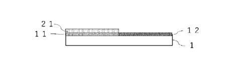
- FIGS. 1 to 3 are cross-sectional views each showing a preparation step, a surface modification step, and a film formation step, respectively.
- the material of the substrate 1 is not particularly limited as long as it is a substrate used in the semiconductor manufacturing process, but may be composed of, for example, silicon, silicon carbide, multiple components containing silicon element, sapphire, various compound semiconductors, etc.
- the substrate 1 may also be, for example, a wafer.
- the substrate 1 may have an uneven structure (not shown) formed on the surface of the substrate.
- the relief structure may be, for example, a three-dimensional structure having one or more structures arranged along the vertical direction of the substrate surface 1a and/or one or more structures arranged along a horizontal direction perpendicular to the vertical direction. Examples of such three-dimensional structures may constitute at least a part of a logic device, a memory device, a gate electrode, etc., such as a FinFET, a nanowire FET, a nanosheet FET, or other multi-gate type FET, a three-dimensional memory cell, etc.
- the first surface 11 and the second surface 12 may be arranged along the planar direction of the substrate surface 1a, or along a direction perpendicular to the substrate surface 1a. According to this embodiment, not only two-dimensional selective processing on a flat surface is possible, but also three-dimensional selective processing on a three-dimensional structure (three-dimensional film formation, three-dimensional etching, etc.).
- the first surface 11 and the second surface 12 may be formed adjacent to each other, or may be formed spaced apart from each other.
- the first surface 11 and the second surface 12 may each be composed of one region or two or more multiple regions. In each surface, the multiple regions may be formed spaced apart from each other, and the surface materials constituting the multiple regions may be the same or different from one another.
- the first surface 11 is a surface having Si elements, and the water repellency of the surface is selectively improved by a silylation agent.
- materials containing Si element include silicon oxide, silicon nitride, silicon carbide, single crystal silicon, polysilicon, silicon germanium, low-k materials, etc. Also, oxides, nitrides, carbides, and other compounds of Si and at least one element selected from the group consisting of N, C, and metal elements may be used.
- the low-k material refers to an insulating material with a dielectric constant lower than SiO2 , and examples of such materials include SiON, SiCN, SiCO, SiCOH, and SiOCN.
- the first surface 11 preferably contains one or more elements selected from the group consisting of Si, N, C, and O (including at least Si). Within the above range, the silylation agent is more likely to form bonds, and water repellency is more likely to be improved. In addition, it is preferable that the surface contains many regions having Si-OH bonds, and a surface in which Si-OH bonds have been formed by surface treatment may be used.
- the first surface 11 may contain Si and O elements, and the total amount of Si and O may be 80 mol % or more with respect to the elements constituting the first surface 11.
- the first surface 11 may contain elements other than Si, N, C, and O (H, P, B, etc.) as long as the water repellency imparted by contact with the chemical solution is not significantly impaired.
- First surface 11 and second surface 12 may be the surfaces of components made of the above materials, or may be configured as the surfaces of films formed from the above materials. In addition, both the surfaces of components made of the above materials and the surfaces of films formed from the above materials may exist.
- the silylation treatment involves contacting at least the first surface 11 and the second surface 12 with a chemical solution, which will be described later.
- the chemical solution may be supplied once or twice or more, but it is preferable to supply it once from the viewpoint of improving the efficiency of the manufacturing process.
- the silylation agent contained in the chemical solution supplied the first and second times may be the same or different, but it is preferable to use the same agent, as this may make it easier to suppress variation and improve work efficiency.
- the silylation treatment forms a water-repellent film 21 on the first surface 11.
- the water-repellent film 21 on the first surface 11 may be composed of a film that covers at least a part of or the entirety of the surface.
- the water-repellent film 21 formed on the first surface 11 preferably has a high water contact angle, and may be, for example, 75° or more. It may also be preferably 78° or more, more preferably 80° or more, and further preferably 84° or more.
- the water repellency of the first surface may be selectively improved if the second surface 12 exhibits a water contact angle that is 10° or more lower than the water contact angle of the first surface 11.
- the water contact angle may be more preferably 15° or more, and even more preferably 20° or more.
- the chemical solution can be supplied in liquid or vapor state, but it is preferable to supply it in liquid state, as this makes it easier to suppress fluctuations in the chemical solution composition when it comes into contact with the first surface 11 and the second surface 12.
- the supply method may be a known method, and examples of the method include a sheet-type method such as spin coating when the material is supplied in a liquid state, and a batch method such as immersion when the material is supplied as a vapor and becomes a liquid after contact with first surface 11 and second surface 12.
- a known vapor injection method may be used.
- the second surface 12 is a surface that basically does not have Si-OH bonds, a water-repellent film is hardly formed, but even if a water-repellent film is not formed, the water repellency may be increased by having a structure in which a compound derived from the silylation agent is physically bonded (for example, attached or adsorbed) to the surface. Furthermore, if a small amount of Si-OH bonds are contained, the silylation agent may bond to these parts as reaction points, and a water-repellent film may be formed locally. In either case, the manifestation of the partial water repellency described above can be removed or reduced by various cleaning methods or the desilylation treatment described below.
- the silylation treatment may be performed by applying known means such as heating, reducing pressure, or drying to promote the silylation reaction between the silylating agent and the OH groups on the surface.
- pretreatment examples include a treatment to remove a natural oxide film from the first surface 11, and a treatment to bond OH groups to at least a portion of the Si in the first surface 11.
- the pretreatment needs to be performed on at least the first surface 11, but may be performed on both the first surface 11 and the second surface 12 as long as it does not adversely affect the second surface 12. If the second surface 12 is oxidized by the pretreatment treatment to bond OH groups, a known reduction treatment or the like may be performed after the silylation treatment to remove the oxygen bonded by the pretreatment from the second surface 12.
- the desilylation process may involve, for example, using a remover to remove the compounds derived from the silylation agent and the water-repellent film that are attached to the second surface 12 while leaving the water-repellent film 21 on the first surface 11.
- the cleaning agent may include an aqueous cleaning solution and/or a rinsing solution.
- the aqueous cleaning solution is not particularly limited as long as it is capable of leaving at least the water-repellent film 21 formed on the first surface 11 behind.
- Examples include water, alcohol, an aqueous hydrogen peroxide solution, and ozone water. These may be used alone or in combination of two or more.
- the drying process may be carried out using known methods such as spin drying, IPA (2-propanol) vapor drying, Marangoni drying, heat drying, air drying, hot air drying, vacuum drying, etc.
- a film material is selectively supplied in a gas phase to the second surface 12 shown in FIG. 3 to form a film.
- the first gas phase reactive material includes a film material.
- the first gas phase reactive material includes organic metals, metal halides, metal oxide halides, etc., and specifically includes tantalum pentaethoxide, tetrakis(dimethylamino)titanium, pentakis(dimethylamino)tantalum, tetrakis(dimethylamino)zirconium, tetrakis(dimethylamino) hafnium, tetrakis(dimethylamino)silane, bis(hexafluoroacetylacetonato)copper, Zn(C2H5)2, Zn(CH3)2 , TMA ( trimethylaluminum ), TaCl5 , WF6 , WOCl4 , CuCl, ZrCl4 , AlCl3 , TiCl4 , SiCl4 , HfCl4 , etc.
- Films formed by atomic layer deposition are not particularly limited, and examples of the films include films containing pure elements (e.g., Si, Cu, Ta, W), films containing oxides (e.g., SiO2 , GeO2 , HfO2, ZrO2 , Ta2O5 , TiO2 , Al2O3 , ZnO, SnO2 , Sb2O5 , B2O3 , In2O3 , WO3 ) , films containing nitrides (e.g., Si3N4 , TiN , AlN, BN, GaN, NbN ), films containing carbides (e.g., SiC), films containing sulfides (e.g., CdS, ZnS, MnS, WS2 ) , and the like.
- pure elements e.g., Si, Cu, Ta, W
- films containing oxides e.g., SiO2 , GeO2 , Hf
- R 1 's are each independently an organic group containing a hydrocarbon group having 1 to 18 carbon atoms in which some or all of the hydrogen atoms may be replaced by fluorine atoms
- X's are each independently a monovalent organic group in which the atom bonded to the Si atom is nitrogen, oxygen, carbon, or halogen
- a is an integer of 1 to 3
- b is an integer of 0 to 2
- the sum of a and b is 1 to 3.
- the silicon compound preferably contains a short-chain silylating agent in which the R 1 in the general formula [1] is each independently an organic group containing a hydrocarbon group having 1 to 8 carbon atoms in which some or all of the hydrogen atoms may be replaced by fluorine atoms. More preferably, the silicon compound may contain a short-chain silylating agent which is an organic group containing a hydrocarbon group having 1 to 7 carbon atoms.
- water-repellent films using long-chain silylating agents have a high water contact angle, when they are formed into complex patterns, there is a concern that the degree of adhesion may vary depending on the method of supplying the agent to the surface, resulting in unstable protective performance. Short-chain silylating agents can stabilize such protective performance. Although the detailed mechanism is unclear, it is presumed that this is because short-chain silylating agents are more likely to diffuse over the surface after being supplied than long-chain silylating agents.
- the monovalent organic group in which the atom bonded to the Si atom is nitrogen, oxygen, or carbon may contain not only hydrogen, carbon, nitrogen, and oxygen atoms, but also silicon, sulfur, halogen atoms, etc.
- N-trimethylsilylacetamide, N-trimethylsilyltrifluoroacetamide, N-methyl-N-trimethylsilylacetamide, N-methyl-N-trimethylsilyltrifluoroacetamide, bis(trimethylsilyl)acetamide, bis(trimethylsilyl)trifluoroacetamide, etc.) are exemplified.
- R a16 represents a saturated or unsaturated alkyl group, a saturated or unsaturated cycloalkyl group, or a fluorine-containing alkyl group.
- R2 is the same as R1
- X is the same as in the above general formula [1]
- c is an integer of 1 to 3
- d is an integer of 0 to 2
- the sum of c and d is 1 to 3.
- the solvent contained in the drug solution is preferably substantially only an aprotic solvent. Also, multiple aprotic solvents may be used. Specifically, assuming that the total solvent contained in the drug solution is 100, it is preferable that 90% by mass or more is an aprotic solvent, more preferably 95% by mass or more, even more preferably 98% by mass or more, and even more preferably 99.5% by mass or more.
- the chemical solution of this embodiment is obtained by mixing and dissolving the above-mentioned components.
- the obtained mixture i.e., solution
- the obtained mixture may be purified using an adsorbent, filter, etc., as necessary.
- Each component may also be purified in advance by distillation, or by using an adsorbent, filter, etc.
- the chemical used in the second embodiment does not substantially contain the catalytic compound.
- the chemical used in the second embodiment does not substantially contain the catalytic compound, it is relatively easy to suppress the fluctuation of the chemical composition when it contacts the first surface 11 and the second surface 12, so it is preferable to vaporize the chemical and then supply the vapor of the chemical to the first surface 11 and the second surface 12.
- the supply method at this time is as described above, and a known steam injection method can be used. Even when supplied as a vapor, the silylation agent adheres to the first surface 11 and the second surface 12 after contacting with them as a liquid, and at least the first surface is subjected to a silylation treatment.
- the fourth embodiment will be described below. Note that descriptions that overlap with the first embodiment will be omitted, and only the differences will be described below.
- the method for treating a substrate in the fourth embodiment includes a preparation step of preparing a substrate having a first surface containing a Si element and a second surface containing no Si element but a metal element; a surface modification step of supplying a chemical solution containing a silylation agent, a catalytic compound, and an aprotic solvent to the first surface and the second surface to selectively improve the water repellency of the first surface relative to the second surface; and an etching step of performing wet etching or dry etching on the second surface.
- a method for treating a substrate according to 1. comprising: The method for treating a substrate, wherein the catalytic compound comprises one or more compounds selected from the group consisting of trimethylsilyl trifluoroacetate, trimethylsilyl trifluoromethanesulfonate, dimethylsilyl trifluoroacetate, dimethylsilyl trifluoromethanesulfonate, butyldimethylsilyl trifluoroacetate, butyldimethylsilyl trifluoromethanesulfonate, hexyldimethylsilyl trifluoroacetate, hexyldimethylsilyl trifluoromethanesulfonate, octyldimethylsilyl trifluoroacetate, octyldimethylsilyl trifluoromethanesulfonate, decyldimethylsilyl trifluoroacetate, and decyldimethylsilyl trifluoromethanes
- a method for treating a substrate according to 1. or 2. comprising: The method for treating a substrate, wherein the silylating agent contains a silicon compound represented by the following general formula [1]: R 1 a Si(H) b X 4-a-b [1] (In the above general formula [1], R 1 is each independently an organic group containing a hydrocarbon group having 1 to 18 carbon atoms in which some or all of the hydrogen atoms may be replaced by fluorine atoms, X is each independently a monovalent organic group in which the atom bonded to the Si atom is nitrogen, oxygen, carbon, or halogen, a is an integer of 1 to 3, b is an integer of 0 to 2, and the sum of a and b is 1 to 3.) 4.
- R 1 is each independently an organic group containing a hydrocarbon group having 1 to 18 carbon atoms in which some or all of the hydrogen atoms may be replaced by fluorine atoms
- X is each independently a monovalent organic group in which the atom bonded
- the method for treating a substrate, wherein the film forming step is a step of forming a film by an atomic layer deposition method.
- the method for treating a substrate according to any one of 1. to 6. The method for treating a substrate, further comprising carrying out a cleaning treatment for cleaning the substrate between the surface modification step and the film formation step.
- a method for treating a substrate according to any one of 1. to 7. A method for treating a substrate, comprising carrying out a drying treatment for drying the substrate between the surface modification step and the film formation step.
- the surface modification step is a method for treating a substrate, the chemical solution being supplied in a liquid state to the first surface and the second surface. 10.
- the chemical solution contains a silylating agent in an amount of 8% by mass or more based on the total amount of the chemical solution.
- Examples 1 to 11, Comparative Examples 1 to 5 Compound 1 (silylation agent) and compound 2 (catalytic compound and/or nitrogen-containing heterocyclic compound) were dissolved in a solvent (aprotic solvent) so as to have the components and contents shown in Table 1, thereby obtaining a drug solution.
- the contents in Table 1 refer to the ratio of the content of each component when the total amount of the chemical solution is 100 mass %.
- Example 11 In Example 11, the coupon was placed horizontally in a steam treatment chamber, and the composition in solution state prepared above was vaporized under the steam supply conditions described below, and the vapor was supplied to the steam treatment chamber.
- Each of the dried coupons obtained by the above immersion or vapor method was placed on a horizontal surface, and 2 ⁇ l of pure water was placed on the main surface of each coupon at room temperature.
- water contact angle was measured using a contact angle meter (CA-X model, manufactured by Kyowa Interface Science).
- XPS X-ray photoelectron spectrometer
- Example 11 the coupon was placed horizontally in the steam treatment chamber, and the composition in solution state prepared above was vaporized under the steam supply conditions described below, and the vapor was supplied to the steam treatment chamber.
- Conditions for supplying the above composition in vapor The above-prepared solution-state composition was dropped at a rate of 0.01 g/sec into a vaporization chamber heated to 165° C. while flowing nitrogen gas at a flow rate of 2 dm 3 /min, and the entire amount was vaporized. The vapor was immediately supplied to the vapor treatment chamber by the nitrogen gas flow. The treatment was carried out for 40 seconds. The vapor supplied to the coupon surface was then converted to liquid to perform a surface modification process.
- the coupon was then immersed in 2-propanol at room temperature for 1 minute, then immersed in ion-exchanged water at room temperature for 1 minute, and dried by spraying N2 gas on the surface for 10 seconds to obtain an evaluation coupon (cleaning and drying process).
- a coupon having a Cu surface as its main surface and each blank coupon were prepared in the same manner as the coupons used for measuring the water contact angle.
- the peak area of nitrogen element (hereinafter referred to as N peak area) was obtained from the XPS spectrum of each film surface obtained by the above immersion method or vapor method. Then, for each film, the N peak area ratio was calculated when the N peak area on the blank substrate surface was set to 1.0. The results are shown in Table 1.
- Example 2 Evaluation of film formation
- a sample was subjected to the following ⁇ Substrate treatment> on the SiO2 film (first surface) and the Cu surface (second surface).
- the sample was placed on a pedestal in the device, and a film formation process was performed using an ALD device (manufactured by Picosun) under the following ⁇ Film formation conditions>.
- a silicon wafer having no uneven pattern on its surface and a silicon oxide film with a thickness of 1 ⁇ m was cut to prepare a number of coupons (test pieces) made of silicon substrates with the dimensions of length, width, and thickness of 4 cm, 1 cm, and 0.75 mm.
- the surface on which the silicon oxide film was formed was regarded as the "principal surface” for the evaluation.
- [Immersion method: Examples 1 to 10, Comparative Examples 1 to 5] The obtained coupon was immersed in 0.5% by mass hydrofluoric acid at 25 ° C for 1 minute, then immersed in ion-exchanged water at room temperature for 1 minute, and dried by spraying N2 gas on the surface for 10 seconds. Next, it was immersed in the prepared chemical solution at 60 ° C for 1 minute to perform a surface modification process. Next, it was immersed in 2-propanol at room temperature for 1 minute, then immersed in ion-exchanged water at room temperature for 1 minute, and dried by spraying N2 gas on the surface for 10 seconds to obtain an evaluation coupon.
- the coupon was then immersed in 2-propanol at room temperature for 1 minute, then immersed in ion-exchanged water at room temperature for 1 minute, and dried by spraying N2 gas on the surface for 10 seconds to obtain an evaluation coupon (cleaning and drying process).
- the treatment methods of the substrates of Examples 1 to 11 can reduce the amount of residual nitrogen-containing components on the metal surface (second surface) that does not contain Si but contains metal, compared to Comparative Examples 1 to 5.
- the film formation was suppressed on the SiO 2 film (first surface), while the film formation was confirmed on the Cu surface (second surface). Therefore, it was found that the substrate treatment methods of Examples 1 to 11 are capable of selectively forming a film on the second surface that does not contain Si and contains metal, compared to the first surface that contains Si.
Landscapes
- Chemical & Material Sciences (AREA)
- General Chemical & Material Sciences (AREA)
- Chemical Kinetics & Catalysis (AREA)
- Engineering & Computer Science (AREA)
- Materials Engineering (AREA)
- Mechanical Engineering (AREA)
- Metallurgy (AREA)
- Organic Chemistry (AREA)
- Chemical Vapour Deposition (AREA)
- Chemically Coating (AREA)
- Materials Applied To Surfaces To Minimize Adherence Of Mist Or Water (AREA)
- Application Of Or Painting With Fluid Materials (AREA)
Priority Applications (2)
| Application Number | Priority Date | Filing Date | Title |
|---|---|---|---|
| KR1020257024915A KR20250132506A (ko) | 2022-12-28 | 2023-12-20 | 기재의 처리 방법 및 기재의 제조 방법 |
| JP2024567675A JPWO2024143097A1 (https=) | 2022-12-28 | 2023-12-20 |
Applications Claiming Priority (2)
| Application Number | Priority Date | Filing Date | Title |
|---|---|---|---|
| JP2022-212245 | 2022-12-28 | ||
| JP2022212245 | 2022-12-28 |
Publications (1)
| Publication Number | Publication Date |
|---|---|
| WO2024143097A1 true WO2024143097A1 (ja) | 2024-07-04 |
Family
ID=91717413
Family Applications (1)
| Application Number | Title | Priority Date | Filing Date |
|---|---|---|---|
| PCT/JP2023/045646 Ceased WO2024143097A1 (ja) | 2022-12-28 | 2023-12-20 | 基材の処理方法および基材の製造方法 |
Country Status (4)
| Country | Link |
|---|---|
| JP (1) | JPWO2024143097A1 (https=) |
| KR (1) | KR20250132506A (https=) |
| TW (1) | TW202432868A (https=) |
| WO (1) | WO2024143097A1 (https=) |
Citations (5)
| Publication number | Priority date | Publication date | Assignee | Title |
|---|---|---|---|---|
| JP2013207220A (ja) * | 2012-03-29 | 2013-10-07 | Dainippon Screen Mfg Co Ltd | 基板処理方法および基板処理装置 |
| JP2019121777A (ja) * | 2017-12-28 | 2019-07-22 | 東京応化工業株式会社 | 表面処理方法、表面処理剤、及び基板上に領域選択的に製膜する方法 |
| WO2019193967A1 (ja) * | 2018-04-05 | 2019-10-10 | セントラル硝子株式会社 | ウェハの表面処理方法及び該方法に用いる組成物 |
| WO2021235476A1 (ja) * | 2020-05-21 | 2021-11-25 | セントラル硝子株式会社 | 半導体基板の表面処理方法、及び表面処理剤組成物 |
| WO2023127942A1 (ja) * | 2021-12-28 | 2023-07-06 | セントラル硝子株式会社 | 膜形成用組成物、および基板の製造方法 |
-
2023
- 2023-12-20 WO PCT/JP2023/045646 patent/WO2024143097A1/ja not_active Ceased
- 2023-12-20 KR KR1020257024915A patent/KR20250132506A/ko active Pending
- 2023-12-20 JP JP2024567675A patent/JPWO2024143097A1/ja active Pending
- 2023-12-22 TW TW112150319A patent/TW202432868A/zh unknown
Patent Citations (5)
| Publication number | Priority date | Publication date | Assignee | Title |
|---|---|---|---|---|
| JP2013207220A (ja) * | 2012-03-29 | 2013-10-07 | Dainippon Screen Mfg Co Ltd | 基板処理方法および基板処理装置 |
| JP2019121777A (ja) * | 2017-12-28 | 2019-07-22 | 東京応化工業株式会社 | 表面処理方法、表面処理剤、及び基板上に領域選択的に製膜する方法 |
| WO2019193967A1 (ja) * | 2018-04-05 | 2019-10-10 | セントラル硝子株式会社 | ウェハの表面処理方法及び該方法に用いる組成物 |
| WO2021235476A1 (ja) * | 2020-05-21 | 2021-11-25 | セントラル硝子株式会社 | 半導体基板の表面処理方法、及び表面処理剤組成物 |
| WO2023127942A1 (ja) * | 2021-12-28 | 2023-07-06 | セントラル硝子株式会社 | 膜形成用組成物、および基板の製造方法 |
Also Published As
| Publication number | Publication date |
|---|---|
| TW202432868A (zh) | 2024-08-16 |
| JPWO2024143097A1 (https=) | 2024-07-04 |
| KR20250132506A (ko) | 2025-09-04 |
Similar Documents
| Publication | Publication Date | Title |
|---|---|---|
| JP7194525B2 (ja) | 表面処理方法、表面処理剤、及び基板上に領域選択的に製膜する方法 | |
| EP4535406A1 (en) | Substrate processing method, and substrate manufacturing method | |
| JP7428777B2 (ja) | 表面処理方法、表面処理剤、及び基板上に領域選択的に製膜する方法 | |
| EP4459666A1 (en) | Composition for film formation and method for producing substrate | |
| JP7727202B2 (ja) | 半導体基板の表面処理方法、及び表面処理剤組成物 | |
| EP4535405A1 (en) | Substrate processing method and substrate production method | |
| WO2024143097A1 (ja) | 基材の処理方法および基材の製造方法 | |
| JP7727203B2 (ja) | 半導体基板の表面処理方法、及び表面処理剤組成物 | |
| WO2026063320A1 (ja) | ウェハの製造方法、加熱蒸散用の表面処理組成物、表面処理組成物の使用方法、蒸気組成物および蒸気組成物の製造方法 | |
| WO2026014135A1 (ja) | 半導体装置の製造方法、基材、およびシリル化組成物 | |
| CN121153104A (zh) | 膜形成用组合物、基板的制造方法及膜形成用组合物的制造方法 | |
| JP7097482B1 (ja) | 表面処理剤、表面処理方法及び基板表面の領域選択的製膜方法 | |
| WO2025182440A1 (ja) | 基材の製造方法、および含Ge酸化物用エッチング液 |
Legal Events
| Date | Code | Title | Description |
|---|---|---|---|
| 121 | Ep: the epo has been informed by wipo that ep was designated in this application |
Ref document number: 23911877 Country of ref document: EP Kind code of ref document: A1 |
|
| WWE | Wipo information: entry into national phase |
Ref document number: 2024567675 Country of ref document: JP |
|
| ENP | Entry into the national phase |
Ref document number: 1020257024915 Country of ref document: KR Free format text: ST27 STATUS EVENT CODE: A-0-1-A10-A15-NAP-PA0105 (AS PROVIDED BY THE NATIONAL OFFICE) |
|
| NENP | Non-entry into the national phase |
Ref country code: DE |
|
| 122 | Ep: pct application non-entry in european phase |
Ref document number: 23911877 Country of ref document: EP Kind code of ref document: A1 |