WO2024142606A1 - 積層セラミック電子部品 - Google Patents
積層セラミック電子部品 Download PDFInfo
- Publication number
- WO2024142606A1 WO2024142606A1 PCT/JP2023/039923 JP2023039923W WO2024142606A1 WO 2024142606 A1 WO2024142606 A1 WO 2024142606A1 JP 2023039923 W JP2023039923 W JP 2023039923W WO 2024142606 A1 WO2024142606 A1 WO 2024142606A1
- Authority
- WO
- WIPO (PCT)
- Prior art keywords
- layer
- plated
- wraparound
- plating
- conductive resin
- Prior art date
- Legal status (The legal status is an assumption and is not a legal conclusion. Google has not performed a legal analysis and makes no representation as to the accuracy of the status listed.)
- Ceased
Links
Images




Classifications
-
- H—ELECTRICITY
- H01—ELECTRIC ELEMENTS
- H01G—CAPACITORS; CAPACITORS, RECTIFIERS, DETECTORS, SWITCHING DEVICES, LIGHT-SENSITIVE OR TEMPERATURE-SENSITIVE DEVICES OF THE ELECTROLYTIC TYPE
- H01G4/00—Fixed capacitors; Processes of their manufacture
- H01G4/002—Details
- H01G4/228—Terminals
- H01G4/232—Terminals electrically connecting two or more layers of a stacked or rolled capacitor
- H01G4/2325—Terminals electrically connecting two or more layers of a stacked or rolled capacitor characterised by the material of the terminals
-
- H—ELECTRICITY
- H01—ELECTRIC ELEMENTS
- H01G—CAPACITORS; CAPACITORS, RECTIFIERS, DETECTORS, SWITCHING DEVICES, LIGHT-SENSITIVE OR TEMPERATURE-SENSITIVE DEVICES OF THE ELECTROLYTIC TYPE
- H01G4/00—Fixed capacitors; Processes of their manufacture
- H01G4/002—Details
- H01G4/005—Electrodes
- H01G4/012—Form of non-self-supporting electrodes
-
- H—ELECTRICITY
- H01—ELECTRIC ELEMENTS
- H01G—CAPACITORS; CAPACITORS, RECTIFIERS, DETECTORS, SWITCHING DEVICES, LIGHT-SENSITIVE OR TEMPERATURE-SENSITIVE DEVICES OF THE ELECTROLYTIC TYPE
- H01G4/00—Fixed capacitors; Processes of their manufacture
- H01G4/002—Details
- H01G4/018—Dielectrics
- H01G4/06—Solid dielectrics
- H01G4/08—Inorganic dielectrics
- H01G4/12—Ceramic dielectrics
-
- H—ELECTRICITY
- H01—ELECTRIC ELEMENTS
- H01G—CAPACITORS; CAPACITORS, RECTIFIERS, DETECTORS, SWITCHING DEVICES, LIGHT-SENSITIVE OR TEMPERATURE-SENSITIVE DEVICES OF THE ELECTROLYTIC TYPE
- H01G4/00—Fixed capacitors; Processes of their manufacture
- H01G4/002—Details
- H01G4/228—Terminals
- H01G4/232—Terminals electrically connecting two or more layers of a stacked or rolled capacitor
-
- H—ELECTRICITY
- H01—ELECTRIC ELEMENTS
- H01G—CAPACITORS; CAPACITORS, RECTIFIERS, DETECTORS, SWITCHING DEVICES, LIGHT-SENSITIVE OR TEMPERATURE-SENSITIVE DEVICES OF THE ELECTROLYTIC TYPE
- H01G4/00—Fixed capacitors; Processes of their manufacture
- H01G4/002—Details
- H01G4/228—Terminals
- H01G4/252—Terminals the terminals being coated on the capacitive element
-
- H—ELECTRICITY
- H01—ELECTRIC ELEMENTS
- H01G—CAPACITORS; CAPACITORS, RECTIFIERS, DETECTORS, SWITCHING DEVICES, LIGHT-SENSITIVE OR TEMPERATURE-SENSITIVE DEVICES OF THE ELECTROLYTIC TYPE
- H01G4/00—Fixed capacitors; Processes of their manufacture
- H01G4/30—Stacked capacitors
Definitions
- the present invention relates to multilayer ceramic electronic components.
- the present invention aims to provide a multilayer ceramic electronic component that can suppress migration caused by filler materials such as Ag contained in resin electrodes, and thus suppress the occurrence of short circuits between electrodes.
- each dielectric layer is preferably 0.5 ⁇ m or more and 10 ⁇ m or less.
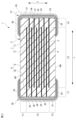
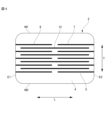
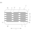
- the second internal electrode layer 7 includes a second opposing electrode portion 9 that faces the first internal electrode layer 6, and a second extraction electrode portion 11 that is extended from the second opposing electrode portion 9 to the second end face E2 of the laminate 2.
- the end of the second extraction electrode portion 11 on the second end face E2 side is extended to the surface of the second end face E2 of the laminate 2.
- the end of the second extraction electrode portion 11 that is extended to the second end face E2 is exposed at the second end face E2.
- each of the first internal electrode layer 6 and the second internal electrode layer 7 is preferably, for example, about 0.2 ⁇ m or more and 2.0 ⁇ m or less.
- the total number of the first internal electrode layers 6 and the second internal electrode layers 7 is preferably 15 or more and 200 or less.
- the external electrodes include a first external electrode 20 and a second external electrode 21.
- the first external electrode 20 is connected to the first internal electrode layer 6.
- the first external electrode 20 is disposed from the first end face E1 to a part of the first main surface M1 and a part of the second main surface M2, as well as a part of the first side surface S1 and a part of the second side surface S2.
- the first external electrode 20 includes a first base electrode layer 32, a first conductive resin layer 34, a first inner plating layer 36, and a first outer plating layer 38.
- the second external electrode 21 includes a second base electrode layer 33, a second conductive resin layer 35, a second inner plating layer 37, and a second outer plating layer 39.
- the thickness of the first base electrode layer 32 at the center in the height direction T of the first base electrode layer 32 located on the first end face E1 is preferably, for example, about 10 ⁇ m or more and 150 ⁇ m or less.
- the thickness of the second base electrode layer 37 at the center in the height direction T of the second base electrode layer 37 located on the second end face E2 is preferably, for example, about 10 ⁇ m or more and 150 ⁇ m or less.
- the thickness of the first and second underlying electrode layers 32 and 33 at the center in the length direction L of the first and second underlying electrode layers 32 and 33 located on the first and second main surfaces M1 and M2 and the first and second side surfaces S1 and S2 is, for example, about 5 ⁇ m or more and 50 ⁇ m or less.
- the second conductive resin layer 35 is disposed on the second base electrode layer 33. More specifically, the second conductive resin layer 35 is disposed so as to cover the second base electrode layer 33. An end of the second conductive resin layer 35 is in contact with the laminate 2.
- the metal component contained in the first conductive resin layer 34 and the second conductive resin layer 35 is preferably a metal filler.
- the metal component particularly preferably contains Ag. Ag may be simple Ag or an alloy containing Ag.
- the shape of the metal filler contained in the first conductive resin layer 34 and the second conductive resin layer 35 is not particularly limited.
- the shape of the metal filler may be spherical, flat, etc.
- the metal filler may be a mixture of spherical metal powder and flat metal powder.
- the plating layer includes an inner plating layer and an outer plating layer. That is, the plating layer includes two layers. However, the plating layer may be a single layer or multiple layers.
- the inner plating layer is disposed on the conductive resin layer.
- the inner plating layer covers at least a portion of the conductive resin layer.
- the inner plating layer includes a first inner plating layer 36 and a second inner plating layer 37.
- the first inner plating layer 36 is disposed on the first conductive resin layer 34.
- the second inner plating layer 37 is disposed on the second conductive resin layer 35.
- the first inner plating layer 36 and the second inner plating layer 37 can be Ni plating layers. By using Ni plating layers for the inner plating layers, it is possible to prevent the base electrode layer and the like from being eroded by solder when mounting the multilayer ceramic capacitor 1.
- the first outer plating layer 38 and the second outer plating layer 39 can be Sn plating layers. Sn plating layers have good solder wettability. Therefore, by using a Sn plating layer for the outer plating layer, mounting of the multilayer ceramic capacitor 1 on a substrate or the like can be made easier.
- the metals that are the materials for the inner plating layer and the surface plating layer are not limited to the above examples.
- the plating layer, including the inner plating layer and the surface plating layer can contain at least one selected from metals such as Cu, Ni, Ag, Pd, Au, and Sn, and alloys such as Ag-Pd alloys.
- each plating layer is preferably 3 ⁇ m or more and 9 ⁇ m or less.
- first outer plating layer 38 and the second outer plating layer 39 are described as Sn plating layers. Therefore, the first outer plating layer 38 may be described as the first Sn plating layer 38, and the second outer plating layer 39 may be described as the second Sn plating layer 39.
- the portion where the second Sn plating layer 39 and the laminate 2 contact is located closer to the first end face E1 than the position of the third main surface conductive resin layer 47 closest to the first end face E1.
- the portion where the second Sn plating layer 39 and the laminate 2 come into contact is located closer to the first end face E1 than the position of the third main surface conductive resin layer 47 closest to the first end face E1.
- the portion where the second Sn plating layer 39 contacts the laminate 2 is located closer to the first end face E1 than the position of the second Ni plating layer 37 closest to the first end face E1. In other words, the second Sn plating layer 39 does not extend between the second Ni plating layer 37 and the laminate 2.
- the conductive filler contained in the resin electrode contains Ag.
- This Ag may become ionized when a voltage is applied at high temperatures or when a voltage is applied in a high-temperature, high-humidity environment.
- the ionized Ag may react with reactants such as water or halogens, causing Ag migration.
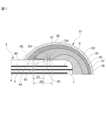
- Figure 8 shows a multilayer ceramic capacitor that does not have a third Ni-plated wraparound layer.
- the component numbers shown in Figure 8 are followed by '. This is to distinguish it from the multilayer ceramic capacitor 1 of this embodiment, which has a third Ni-plated wraparound layer 43.
- the component numbers with the ' removed correspond to the component numbers of this embodiment.
- the multilayer ceramic capacitor 1 of this embodiment has a configuration in which the conductive resin layer 35 is covered with the third Ni-plated wraparound layer 43. This makes it difficult for ionized Ag to react with reactants such as water and halogens. As a result, the occurrence of Ag migration is suppressed.
- the second conductive resin layer 35 covers the second base electrode layer 33, and a portion of the second conductive resin layer 35 is disposed directly on the first main surface M1 of the laminate 2.
- the third Ni-plated wraparound layer 43 is disposed between the second conductive resin layer 35 disposed directly on the first main surface M1 of the laminate 2 and the first main surface M1 of the laminate 2.
- the portion of the third Ni-plated wraparound layer 43 where extension begins on the first main surface M1 toward the second end face E2 is defined as the starting end 44.
- the portion of the third Ni-plated wraparound layer 43 where extension ends on the first main surface M1 toward the second end face E2 is defined as the ending end 45.
- the ending end 45 corresponds to the end of the third Ni-plated wraparound layer 43.
- dimension D1 is the distance in the length direction L from the starting end 44 to the ending end 45 of the third Ni-plated wraparound layer 43.
- Dimension D1 is preferably 5 ⁇ m or more.
- dimension D3 is the distance in the height direction T of the third Ni-plated wraparound layer 43 at the starting end 44 of the third Ni-plated wraparound layer 43.
- Dimension D3 is preferably 2 ⁇ m or more.
- the thickness in the height direction T of the third Ni-plated wraparound layer 43 preferably becomes thinner as the third Ni-plated wraparound layer 43 moves in the length direction L toward the second end face E2.
- the dimension in the height direction T at the end portion 45 of the third Ni-plated wraparound layer 43 is defined as dimension D4.
- dimension D4 will be smaller than dimension D3.
- the laminate 2 can be divided in the width direction W into a first side portion W1, a W opposing electrode portion W2, and a second side portion W3.
- first side portion W1 is also called the first side outer layer portion
- W opposing electrode portion W2 is also called the inner layer portion
- second side portion W3 is also called the second side outer layer portion.
- the portion of the first main surface M1 that corresponds to the first side portion W1 is indicated by arrow A.
- the portion of the first main surface M1 that corresponds to the second side portion W3 is indicated by arrow B.
- the portion of the second main surface M2 that corresponds to the first side portion W1 is indicated by arrow C.
- the portion of the second main surface M2 that corresponds to the second side portion W3 is indicated by arrow D.
- the multilayer ceramic capacitor 1 has a Ni-plated wraparound layer provided on the main surfaces of the first side outer layer portion and the second side outer layer portion.
- the conductive paste for the dielectric sheet and the internal electrodes contains a binder and a solvent.
- Known organic binders and organic solvents can be used as the binder and the solvent.
- the laminated sheet is pressed in the height direction to produce a laminated block. Pressing is performed using a means such as a hydrostatic press.
- the laminated block is cut to a specified size, thereby cutting out laminated chips. At this time, the corners and edges of the laminated chips may be rounded.
- the rounding can be achieved by barrel polishing or the like.
- the laminated chip is fired. This produces a laminate.
- the firing temperature is preferably 900°C or higher and 1400°C or lower. The firing temperature can be changed depending on the materials of the dielectric and internal electrodes.
- the conductive resin layer is formed on the base electrode layer.
- a conductive resin paste is first prepared.
- the conductive resin paste contains a resin component and a metal component.
- This conductive resin paste is applied onto the base electrode layer. This application can be performed by a dipping method.
- a heat treatment is performed at a temperature of 200°C or higher and 550°C or lower. This heat treatment thermally hardens the resin. This forms a conductive electrode layer.
- the atmosphere during the heat treatment is preferably a nitrogen gas atmosphere.
- Ni plating layers are formed on the surface of the conductive resin layer as the first and second inner plating layers.
- the first and second Ni plating layers can be formed by electrolytic plating. It is preferable to use barrel plating as the plating method.
- the conductive resin layer When forming the conductive resin layer, by adjusting at least one of the resin curing temperature and curing time, it is possible to control the shape of the gap between the conductive resin layer and the laminate, where the Ni-plated wrap-around layer will later be placed. For example, a higher curing temperature and a longer curing time make it easier for peeling to occur between the conductive resin layer and the base body, i.e., the laminate. The Ni-plated layer then penetrates into this peeled area.
- a Sn plating layer is further formed on the Ni plating layer. That is, a first Sn plating layer is formed on the first Ni plating layer, and a second Sn plating layer is formed on the second Ni plating layer. This improves the wettability of the solder used for mounting when mounting the multilayer ceramic capacitor on a substrate or the like. As a result, the multilayer ceramic capacitor can be easily mounted on a substrate or the like.
- An electrolytic plating method can be used as a method for forming the Sn plating layer. In addition, it is preferable to use barrel plating as the plating method.
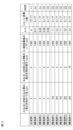
- Base Electrode layer Contains Cu as a conductive metal and a glass component. Thickness of the base electrode layer at the center in the height direction T of the base electrode layer located at the first end face E1 and the second end face E2: 15 ⁇ m Thickness of the base electrode layer at the center in the longitudinal direction L of the base electrode layer located on the first main surface M1, the second main surface M2, and the first side surface S1 and the second side surface S2: 4 ⁇ m
- the chip was polished and resin-hardened, and the cross section of the end of the LT cross section in the W direction was photographed at 5000 times magnification using a SEM.
- the dimensions of the Ni-plated wraparound layer were measured in the photographed image and the average value was calculated.
- the dimension of the chip in the longitudinal direction L was set to 3.2 mm.
- ⁇ 5> the thickness in the height direction of the first Ni-plated wraparound layer and the second Ni-plated wraparound layer becomes thinner toward the first end face in the length direction;
- the thicknesses of the third Ni-plated wraparound layer and the fourth Ni-plated wraparound layer in the height direction become thinner toward the second end surface in the length direction.
- ⁇ 4> The multilayer ceramic electronic component according to any one of ⁇ 1> to ⁇ 4>.
Landscapes
- Engineering & Computer Science (AREA)
- Power Engineering (AREA)
- Manufacturing & Machinery (AREA)
- Microelectronics & Electronic Packaging (AREA)
- Chemical & Material Sciences (AREA)
- Ceramic Engineering (AREA)
- Inorganic Chemistry (AREA)
- Fixed Capacitors And Capacitor Manufacturing Machines (AREA)
- Ceramic Capacitors (AREA)
- Coils Or Transformers For Communication (AREA)
Priority Applications (5)
| Application Number | Priority Date | Filing Date | Title |
|---|---|---|---|
| JP2024567260A JP7800737B2 (ja) | 2022-12-28 | 2023-11-06 | 積層セラミック電子部品 |
| CN202380089060.2A CN120418903A (zh) | 2022-12-28 | 2023-11-06 | 层叠陶瓷电子部件 |
| KR1020257019974A KR102935388B1 (ko) | 2022-12-28 | 2023-11-06 | 적층 세라믹 전자부품 |
| EP23911390.5A EP4600986A1 (en) | 2022-12-28 | 2023-11-06 | Layered ceramic electronic component |
| US19/196,312 US20250259797A1 (en) | 2022-12-28 | 2025-05-01 | Multilayer ceramic electronic component |
Applications Claiming Priority (2)
| Application Number | Priority Date | Filing Date | Title |
|---|---|---|---|
| JP2022-211941 | 2022-12-28 | ||
| JP2022211941 | 2022-12-28 |
Related Child Applications (1)
| Application Number | Title | Priority Date | Filing Date |
|---|---|---|---|
| US19/196,312 Continuation US20250259797A1 (en) | 2022-12-28 | 2025-05-01 | Multilayer ceramic electronic component |
Publications (1)
| Publication Number | Publication Date |
|---|---|
| WO2024142606A1 true WO2024142606A1 (ja) | 2024-07-04 |
Family
ID=91717289
Family Applications (1)
| Application Number | Title | Priority Date | Filing Date |
|---|---|---|---|
| PCT/JP2023/039923 Ceased WO2024142606A1 (ja) | 2022-12-28 | 2023-11-06 | 積層セラミック電子部品 |
Country Status (6)
| Country | Link |
|---|---|
| US (1) | US20250259797A1 (https=) |
| EP (1) | EP4600986A1 (https=) |
| JP (1) | JP7800737B2 (https=) |
| KR (1) | KR102935388B1 (https=) |
| CN (1) | CN120418903A (https=) |
| WO (1) | WO2024142606A1 (https=) |
Citations (4)
| Publication number | Priority date | Publication date | Assignee | Title |
|---|---|---|---|---|
| JPH11162771A (ja) | 1997-11-25 | 1999-06-18 | Kyocera Corp | 積層セラミックコンデンサ |
| JP2010073780A (ja) * | 2008-09-17 | 2010-04-02 | Murata Mfg Co Ltd | セラミック電子部品およびその製造方法 |
| JP2021028938A (ja) * | 2019-08-09 | 2021-02-25 | Tdk株式会社 | 電子部品 |
| JP2021052129A (ja) * | 2019-09-26 | 2021-04-01 | 株式会社村田製作所 | 積層セラミック電子部品 |
Family Cites Families (1)
| Publication number | Priority date | Publication date | Assignee | Title |
|---|---|---|---|---|
| JP2011162771A (ja) | 2010-01-14 | 2011-08-25 | Toray Ind Inc | 二軸配向ポリフェニレンスルフィドフィルムおよびその製造方法 |
-
2023
- 2023-11-06 KR KR1020257019974A patent/KR102935388B1/ko active Active
- 2023-11-06 JP JP2024567260A patent/JP7800737B2/ja active Active
- 2023-11-06 EP EP23911390.5A patent/EP4600986A1/en active Pending
- 2023-11-06 CN CN202380089060.2A patent/CN120418903A/zh active Pending
- 2023-11-06 WO PCT/JP2023/039923 patent/WO2024142606A1/ja not_active Ceased
-
2025
- 2025-05-01 US US19/196,312 patent/US20250259797A1/en active Pending
Patent Citations (4)
| Publication number | Priority date | Publication date | Assignee | Title |
|---|---|---|---|---|
| JPH11162771A (ja) | 1997-11-25 | 1999-06-18 | Kyocera Corp | 積層セラミックコンデンサ |
| JP2010073780A (ja) * | 2008-09-17 | 2010-04-02 | Murata Mfg Co Ltd | セラミック電子部品およびその製造方法 |
| JP2021028938A (ja) * | 2019-08-09 | 2021-02-25 | Tdk株式会社 | 電子部品 |
| JP2021052129A (ja) * | 2019-09-26 | 2021-04-01 | 株式会社村田製作所 | 積層セラミック電子部品 |
Also Published As
| Publication number | Publication date |
|---|---|
| EP4600986A1 (en) | 2025-08-13 |
| CN120418903A (zh) | 2025-08-01 |
| US20250259797A1 (en) | 2025-08-14 |
| KR102935388B1 (ko) | 2026-03-09 |
| JP7800737B2 (ja) | 2026-01-16 |
| JPWO2024142606A1 (https=) | 2024-07-04 |
| KR20250099258A (ko) | 2025-07-01 |
Similar Documents
| Publication | Publication Date | Title |
|---|---|---|
| US10615327B2 (en) | Monolithic ceramic electronic component | |
| US11062848B2 (en) | Multilayer ceramic electronic component | |
| US11361906B2 (en) | Multilayer ceramic electronic component | |
| US12148573B2 (en) | Multilayer ceramic electronic component with a stress applied Ni plated layer | |
| US10242797B2 (en) | Multilayer-ceramic-capacitor mounting structure | |
| KR102950887B1 (ko) | 적층 세라믹 전자부품 | |
| US20250308798A1 (en) | Multilayer ceramic electronic component | |
| JP7800737B2 (ja) | 積層セラミック電子部品 | |
| CN115083654A (zh) | 导电性膏以及陶瓷电子部件 | |
| US20260094766A1 (en) | Multilayer ceramic capacitor | |
| US20260074110A1 (en) | Multilayer ceramic capacitor | |
| KR102946063B1 (ko) | 적층형 전자 부품 | |
| US12609243B2 (en) | Multilayer ceramic capacitor | |
| US20240420893A1 (en) | Multilayer ceramic capacitor | |
| US20260128216A1 (en) | Multilayer ceramic electronic component | |
| US20240249885A1 (en) | Multilayer ceramic electronic component | |
| US20250111995A1 (en) | Multilayer ceramic capacitor | |
| US20250385045A1 (en) | Multilayer ceramic capacitor | |
| WO2024247445A1 (ja) | 積層セラミックコンデンサ | |
| WO2025004487A1 (ja) | 積層セラミックコンデンサ | |
| WO2025047095A1 (ja) | 積層セラミックコンデンサおよび積層セラミックコンデンサの製造方法 | |
| KR20260016613A (ko) | 적층 세라믹 콘덴서 | |
| WO2025126319A1 (ja) | 積層セラミック電子部品 | |
| JP2023122670A (ja) | 積層セラミックコンデンサ | |
| CN121336274A (zh) | 层叠陶瓷电子部件 |
Legal Events
| Date | Code | Title | Description |
|---|---|---|---|
| 121 | Ep: the epo has been informed by wipo that ep was designated in this application |
Ref document number: 23911390 Country of ref document: EP Kind code of ref document: A1 |
|
| WWE | Wipo information: entry into national phase |
Ref document number: 2024567260 Country of ref document: JP |
|
| WWE | Wipo information: entry into national phase |
Ref document number: 2023911390 Country of ref document: EP |
|
| ENP | Entry into the national phase |
Ref document number: 2023911390 Country of ref document: EP Effective date: 20250508 |
|
| ENP | Entry into the national phase |
Ref document number: 20257019974 Country of ref document: KR Kind code of ref document: A |
|
| WWE | Wipo information: entry into national phase |
Ref document number: 1020257019974 Country of ref document: KR Ref document number: 202517057852 Country of ref document: IN |
|
| WWE | Wipo information: entry into national phase |
Ref document number: 202380089060.2 Country of ref document: CN |
|
| WWP | Wipo information: published in national office |
Ref document number: 1020257019974 Country of ref document: KR |
|
| WWP | Wipo information: published in national office |
Ref document number: 202517057852 Country of ref document: IN |
|
| NENP | Non-entry into the national phase |
Ref country code: DE |
|
| WWP | Wipo information: published in national office |
Ref document number: 202380089060.2 Country of ref document: CN |
|
| WWP | Wipo information: published in national office |
Ref document number: 2023911390 Country of ref document: EP |